
 Open Access Article
 This Open Access Article is licensed under a Creative Commons Attribution-Non Commercial 3.0 Unported Licence
Epitaxial growth of 1D GaN-based heterostructures on various substrates for photonic and energy applications
Ameer
Abdullah
,
Mandar A.
Kulkarni
,
Hamza
Thaalbi
 ,
Fawad
Tariq
and
Sang-Wan
Ryu
*
,
Fawad
Tariq
and
Sang-Wan
Ryu
*
Department of Physics, Chonnam National University, Gwangju 61186, Republic of Korea. E-mail: sangwan@chonnam.ac.kr
First published on 18th January 2023
Abstract
GaN is an important III–V semiconductor for a variety of applications owing to its large direct band gap. GaN nanowires (NWs) have demonstrated significant potential as critical building blocks for nanoelectronics and nanophotonic devices, as well as integrated nanosystems. We present a comprehensive analysis of the vapor–liquid–solid (VLS) as a general synthesis technique for NWs on a variety of substrates, the morphological and structural characterization, and applications of GaN NWs in piezoelectric nanogenerators, light-emitting diodes, and solar-driven water splitting. We begin by summarizing the overall VLS growth process of GaN NWs, followed by the growth of NWs on several substrates. Subsequently, we review the various uses of GaN NWs in depth.
1. Introduction
It is universally recognized that silicon (Si) semiconductor devices have reached their physical limits in terms of scalability and physical attributes.1 New materials must be investigated to boost system performance and reliability even more. Gallium nitride (GaN) (a wide-bandgap semiconductor material) is a more suitable choice for this objective. Basic physical and electrical properties of GaN materials such as temperature, frequency, high conductivity, and power operation render this semiconductor a unique material of choice to address the requirements of future advanced systems in the field of radio frequency and power conversion applications.2–4The technological maturity of GaN has substantially increased in recent years; however, much research is required to fully use the capacity of GaN devices while maintaining costs comparable to those of silicon devices and satisfying the high demand for reliability and robustness necessary in application domains (automotive, consumer electronics, defense and aerospace, healthcare, information & communication technology, and industrial & power).5–8
Silicon can be grown from a melt to make native substrates;9–11 however, this is not possible for GaN at normal temperatures and pressures, and as a result, the development of GaN technology has been delayed for many years.1,12,13 Several systems employing foreign substrates such as Si, SiC, or sapphire have been adopted to overcome this barrier.14–17 However, growing on a foreign substrate introduces various faults that limit device performance; hence, much research is being conducted to improve the material for industrial purposes.18–20 Thick crystal growth for substrate production has been developed using halide vapor phase epitaxy (HVPE),21 high nitrogen pressure solution growth (HNPS),22 sodium (Na) flux,23 and the ammonothermal method,24 metalorganic chemical vapor deposition (MOCVD), and molecular beam epitaxy (MBE) are commonly used for device structure growth.25–29
The epitaxial growth process is used to grow GaN and requires growing a single crystalline material on a single crystalline substrate by following the orientation of the planes of the substrate.30–32 Based on the nature of the substrate material, there are two types of epitaxial crystal growth.33 When a crystal grows epitaxially on the same material as the substrate, this is referred to as homoepitaxial growth, whereas crystal growth on a foreign substrate is referred to as heteroepitaxial growth.34 The use of epitaxial growth minimizes growth time,35 wafering costs, and waste produced by growth, cutting, polishing, and other processes.36 The primary benefit of epitaxy is homogeneity in composition, controlled growth parameters, and a better knowledge of the development process itself.37 GaN is always grown on a foreign substrate; thus, it follows a heteroepitaxial growth.38,39 For the formation of the epilayers of III–V compound semiconductors and other materials, several epitaxial processes have been applied.40,41 These techniques include liquid phase epitaxy (LPE), molecular beam epitaxy (MBE), chemical beam epitaxy (CBE), atomic layer epitaxy (ALE), and vapor phase epitaxy (VPE).42,43 Among the above-mentioned epitaxial techniques, VPE is a technique that is used to grow extremely high-quality layers with a high growth rate.44,45 In addition, VPE provides flexibility in the type and level of doping and can be used for large-scale growth.46
The electrical and optical properties of the 1D nanostructures include strong carrier mobility,47–49 a high rate of radiative recombination,50–52 and long-term stability. Therefore, 1D semiconductor nanostructures such as nanowires (NWs), nanorods (NRs), nanopillars, nanocolumns (NCs), and nanotubes (NTs) provide promising potential for the creation of high-performance optoelectronic and electrical devices.53–56
Owing to their use in various applications substantial research has been devoted to the growth of 1D GaN NWs. Traditionally, GaN NWs were grown using MBE or MOCVD. MBE on a heated substrate under an ultra-high vacuum can be used to epitaxially grow high-purity GaN NWs.57 MOCVD growth can be carried out on a heated substrate at a range of vacuum levels varying from a few tens to several hundreds of torr. A carrier gas (normally H2) is used to deliver the Ga and N precursors to the surface of substrate, where they can react and initiate the epitaxial growth. Because the growth rate of MOCVD is substantially faster than that of MBE, high aspect ratio GaN NWs can be created utilizing the former process.58,59
Despite the high growth rate of GaN NWs created by MOCVD, there are various challenges for generating single crystal NWs, including substrate selection, metal catalyst nature, metal catalyst thickness, agglomeration and growth temperature, V/III ratio, reactor pressure, and carrier gas flow.60 Although the selection of the proper substrate is challenging, it is one of the top advantages that NWs can be grown on any foreign substrate. Nature and control over the thickness of metal catalyst help in defining the morphology of NWs. The aspect ratio of NWs is critically dependent on agglomeration conditions. Crystal quality and growth rate are controlled by growth temperature and V/III ratio, respectively. Reactor pressure and carrier gas flow also influence the growth rate and morphology of NWs.61,62 The challenges in terms of the reliability and cost-effectiveness of GaN-based nanostructures for photovoltaic, LED, FET, laser, photoelectrode, and nanogenerator applications are addressed by elimination of stacking faults and threading dislocations through the growth of GaN NWs on various substrates.63
Growing 1D GaN NWs on various substrates is challenging, but it has a vast growth window that allows for the efficient growth of single crystal NWs. The versatility of transporting NWs from the substrate on which they are grown to another material, as well as growth on multiple substrates, allows for a broad range of applications.64
Catalyst-free growth (CFG), selective area growth (SAG), and vapor–liquid–solid (VLS) are well-known fabrication processes for 1D GaN-based nanostructures.65–67 VLS is a method to create one-dimensional nanostructures,68 such as NWs, using chemical vapor phase epitaxy.69–71 In general, the formation of a crystal via direct adsorption of a gas phase onto a solid surface is extremely slow. The VLS method overcomes this problem by including a catalytic liquid alloy phase that can rapidly adsorb a vapor to supersaturation levels, allowing crystal formation to occur from nucleated seeds at the liquid–solid interface.72,73 The size and physical characteristics of the liquid alloy influence the physical properties of the nanostructure created in this manner.74
There are several comprehensive reports on the growth mechanisms of GaN NWs.75–77 In this review, we summarize the VLS growth mechanism of GaN NWs grown by MOCVD on various substrates (sapphire, silicone, copper, tungsten, glass, gallium nitride, and beryllium oxide) for various applications (piezoelectric nanogenerators and sensors, light-emitting diodes, and solar-driven water splitting) by our group and, where necessary, the results with the permission of the publishers are included. We also highlight the prospects of flexibility in substrate selection with VLS growth of GaN NWs for various applications.
2. VLS growth mechanism of GaN NWs
VLS is the most recognized method, initially described by Wagner and Ellis in 1964 based on the formation of Au nanoparticles on the top of a single-crystal silicon nanowire. Reactant vapor, liquid metal catalyst, and solid nanowire product are represented by vapor, liquid, and solid, respectively. The essential elements of the VLS growth mechanism are thoroughly examined, including vapor supersaturation, liquid selection, the liquid–substrate interface, liquid–solid interface, and solid–substrate interface. Vapor supersaturation should be sufficient to dissolve into liquid metal catalyst to generate supersaturated alloys, from which nanowire seed crystals condense. Controlling vapor supersaturation is possible by modifying pressure, temperature, and source material. Metal catalysts, in general, should be properly evaluated based on the alloy phase diagram and chemical reactivity. The interface between the liquid metal catalyst and the substrate should be carefully examined as well. Because the wettability determines the distribution of the liquid metal catalyst, which can be a continuous film, porous film, linked network, isolated islands, or anything else. As a result, the morphology of the products may suffer significantly. Fig. 1 depicts a schematic of the mechanism for VLS growth of GaN NWs by MOCVD. All phases are depicted in order, beginning with thin film deposition and progressing through metal agglomeration, supersaturation, and vertical growth of 1D GaN NWs.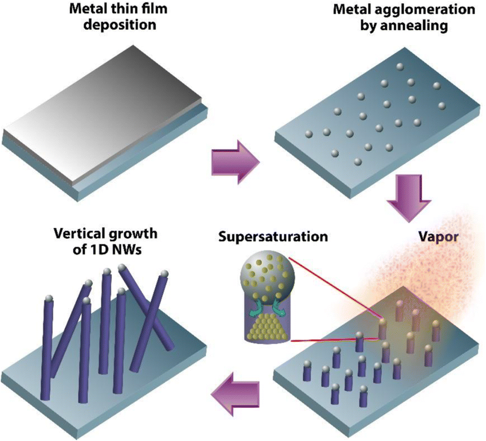 | ||
| Fig. 1 The VLS growth mechanism of 1D NWs. Reproduced with permission from ref. 68. Copyright 2017 IOP publisher. | ||
3. Growth of 1D GaN-based heterostructures (HS) on various substrates
Several factors impact the shape and properties of GaN NWs grown using VLS. Catalyst composition, growth kinetics, and hosting substrate type are among these parameters.78 The influence of the hosting substrate type on the morphology of NWs is investigated in this study.3.1 Growth of 1D GaN/InGaN core/shell MQWs HS on Si
GaN NWs grown using the VLS approach are extremely sensitive to the nature and/or orientation of the hosting substrate. Johar et al. reported for the first time the growth of GaN/InGaN MQW co-axial NWs on an n-type Si (111) substrate for ultrafast carrier dynamics studies.79 For the growth of 1D GaN-based core NWs, Au NPs are deposited on a Si substrate to be used as a metal catalyst. The substrates are placed into the MOCVD after Au colloidal particles are deposited on the Si substrate. Trimethylindium (TMIn) and trimethylgallium (TMGa) are then injected into the reactor as indium and gallium precursors. To achieve the agglomeration of the Au/In/Ga alloy catalyst, the reactor temperature is raised to perform annealing. The m-axial GaN core NWs are grown from the agglomerated alloy particles. Following the successful axial growth of non-polar GaN core NWs using the VLS approach, the mode of growth is switched from VLS to VS for the NWs' lateral growth. The GaN shell is formed radially in the first phase of radial growth. Then, seven pairs of GaN/InGaN MQWs with the same thickness for all GaN/InGaN pairings are grown. Schematically, the entire growth mechanism of core GaN NWs with GaN/InGaN MQW shells is illustrated in Fig. 2(a)–(f). The morphology of GaN core NWs is shown in Fig. 2(g) and a magnified image in the inset demonstrates the smooth surface of grown NWs. The SEM image of GaN/InGaN MQW co-axial NWs is shown in Fig. 2(h). A magnified image of GaN/InGaN MQW co-axial NWs with an equilateral triangular cross-section is shown in the inset.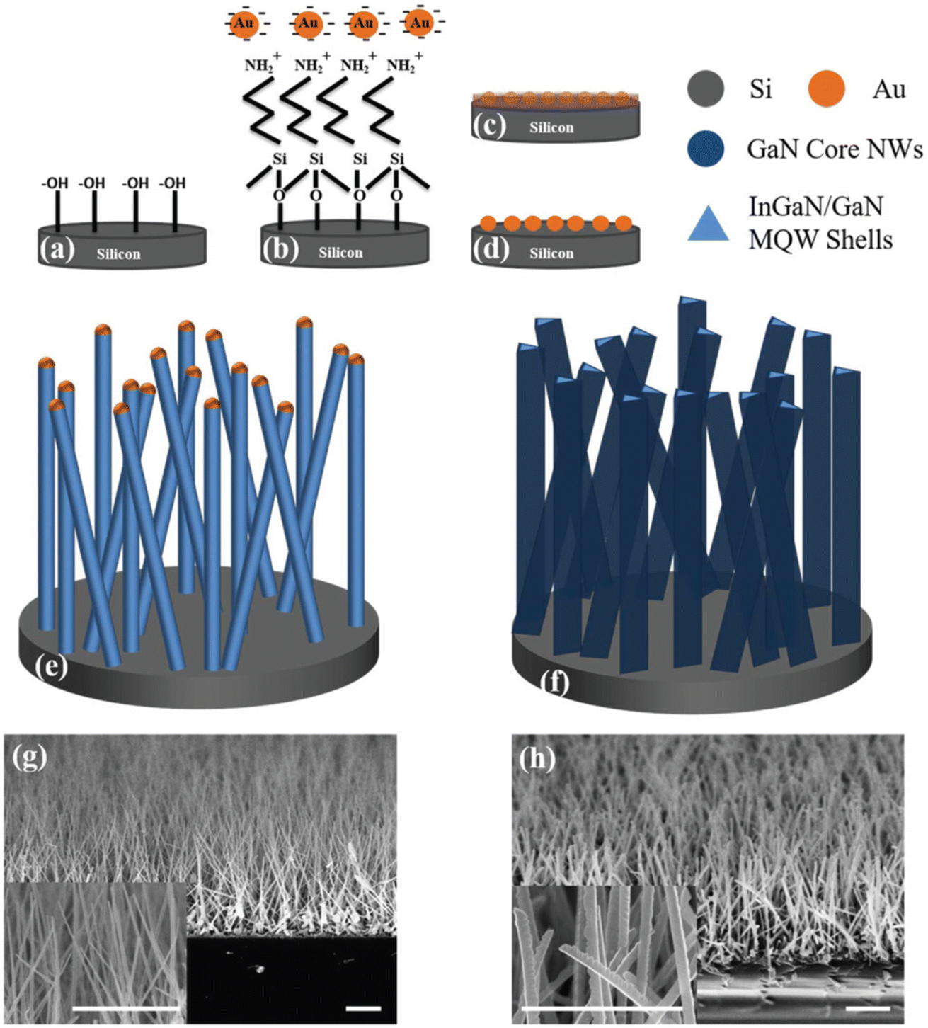 | ||
| Fig. 2 Schematic depiction of catalyst preparation: (a) hydroxylation, (b) silanization and Au NP deposition, (c) in situ Ga and In deposition, and (d) annealing. The schematic for (e) VLS development of GaN core nanowires and (f) lateral growth of GaN/InGaN MQW shells around the GaN core nanowires. SEM images of (g) GaN core NWs and (h) GaN/InGaN MQW coaxial NWs, with insets showing high-magnification images in each case. Reproduced with permission from ref. 79. Copyright 2019 RSC publisher. | ||
Johar et al. furthermore performed high-angle annular dark-field scanning transmission electron microscopy (HAADF-STEM), to investigate the crystallographic structure of the samples. To evaluate the cross-sectional view of the triangular-shaped GaN/InGaN MQW co-axial NWs, a thick slice was sliced by focused ion beam (FIB) from a single NW, as shown in Fig. 3(a)–(c). The shell development of the GaN/InGaN is strongly dependent on the facet orientation of the GaN core, as seen in Fig. 3(c). The HAADF-STEM picture in Fig. 3(c) confirms that GaN/InGaN shells do not grow near the base of the GaN core, which is well known.80 A high-magnification image of the GaN/InGaN MQW grown on semi-polar facets is also presented in Fig. 3(d), with seven pairs of GaN/InGaN MQWs with explicit borders detected. The thickness of the InGaN QW and GaN QB is shown in Fig. 3(e). The inter-planar spacing shown in Fig. 3(f) and SAED pattern in Fig. 3(g) shows that the GaN core grew along [1![[1 with combining macron]](https://www.rsc.org/images/entities/char_0031_0304.gif) 00] with the basal plane of (000
00] with the basal plane of (000![[2 with combining macron]](https://www.rsc.org/images/entities/char_0032_0304.gif) ) and two inclined planes (112) and (22). As a result, it can be concluded that single crystalline GaN NWs can be successfully fabricated on Si substrate by optimizing the growth conditions for several applications.
) and two inclined planes (112) and (22). As a result, it can be concluded that single crystalline GaN NWs can be successfully fabricated on Si substrate by optimizing the growth conditions for several applications.
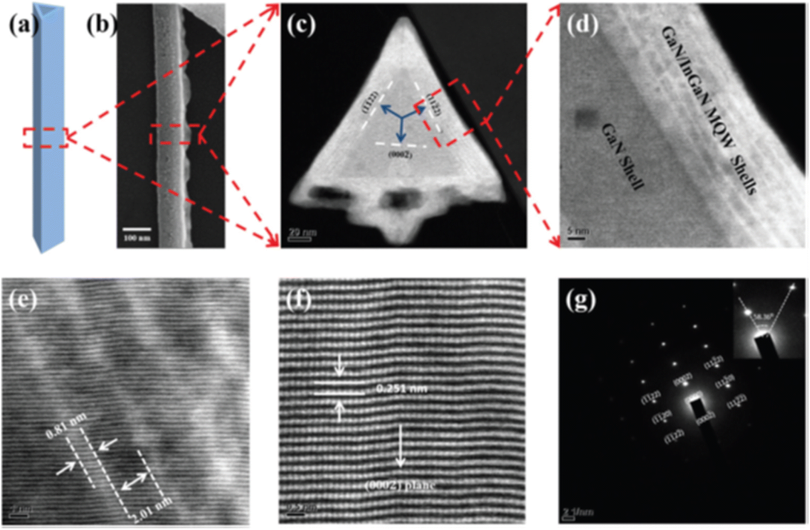 | ||
| Fig. 3 (a) Schematic illustration of a GaN/InGaN MQW co-axial single NW, (b) low-magnification STEM micrograph, in which the growth direction of GaN core NWs is also shown along the m-axis, (c) cross-sectional HAADF-STEM micrograph of a single NW prepared by FIB, (d) layer-by-layer structure of the GaN/InGaN pairs from one side of an isosceles NW, (e) high-magnification micrograph depicting the InGaN QWs, (f) inter-planer measurement of the structure with QWs, and (g) SAED patterns of the GaN/InGaN disk. Reproduced with permission from ref. 79. Copyright 2019 RSC publisher. | ||
3.2 Growth of 1D GaN/InGaN core/shell MQWs HS on beryllium oxide
Beryllium oxide (BeO) is a special type of material that possesses both high thermal conductivity and high electrical resistance. The crystal structure of BeO is identical to that of GaN, and the absolute difference in lattice constants is less than 17%. For the first time, the formation of GaN NWs on a polycrystalline BeO substrate was reported by Johar et al.81 The optimal strategy for growing single-crystalline GaN atop polycrystalline BeO is to generate single-crystalline GaN NWs with the same crystal orientation. The GaN NWs were synthesized on the BeO substrate using the VLS approach employing Au as a catalyst. The schematic illustration of agglomerated alloy NPs in Fig. 4(a) and the SEM image of a bare BeO substrate in Fig. 5(a) show that the BeO substrate is polycrystalline. The GaN NWs were grown when the precursors were injected into the reactor, and their schematics are illustrated in Fig. 4(b). The low- and high-magnification images of the GaN core NWs are shown in Fig. 5(b-i) and (b-ii). It is discovered that NWs grow equally on all grains, regardless of host crystal orientation. The NWs are round, with diameters of 19 ± 2 nm, lengths of 4.4 ± 0.1 μm, and surface densities of (3.4 ± 0.1) ×109 cm−2.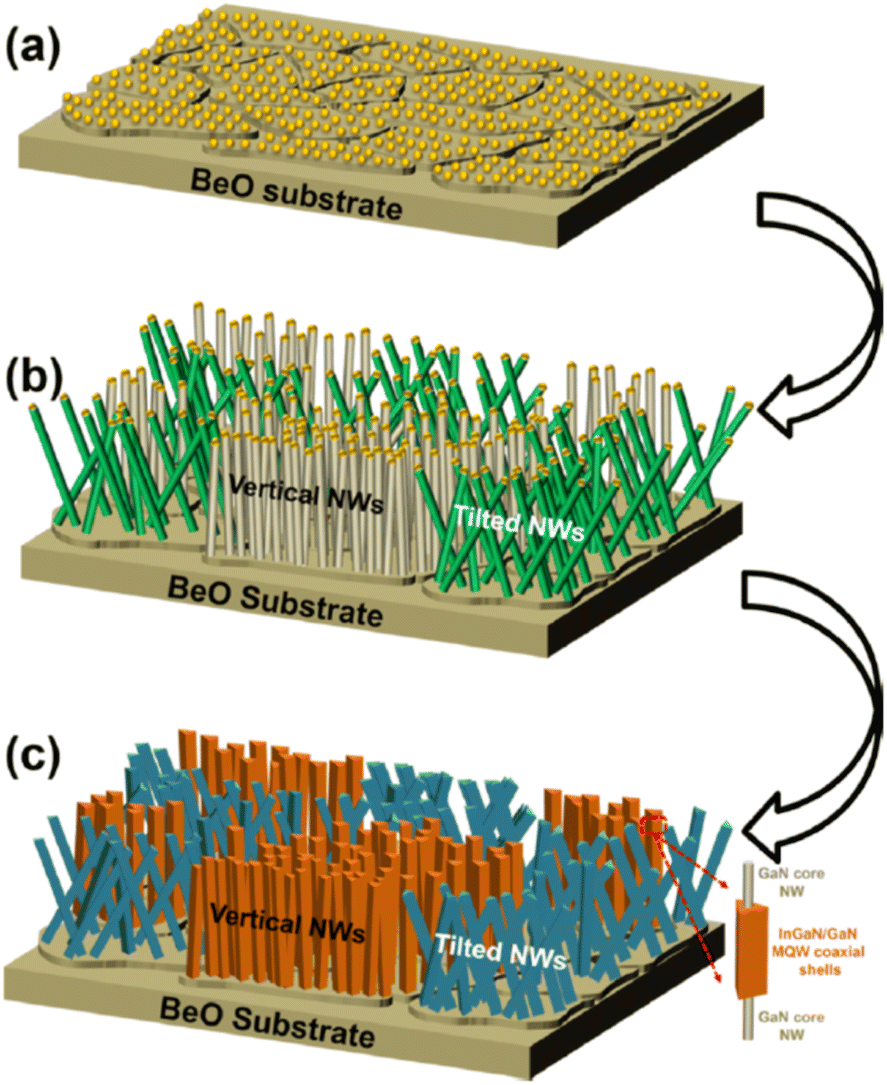 | ||
| Fig. 4 Depicts a schematic representation of the GaN-based NW fabrication flow: (a) aggregation of the Au/Ga/In metal alloy catalyst, (b) formation of the GaN core NWs, and (c) InGaN/GaN MQW coaxial shells on the BeO substrate; the inset indicates the geometry of the core/shell structure. Reproduced with permission from ref. 81. Copyright 2020 ACS publisher. | ||
 | ||
| Fig. 5 Scanning electron micrographs: (a) top view of the bare BeO substrate, with an inset showing a bird's-eye view, (b-i and b-ii) low- to high-magnification images of GaN core NWs, (c-i and c-ii) low- to high-magnification images of InGaN/GaN MQW NWs, (d-i and d-ii) images with an emphasis on the vertical development of the NWs, and (e-i and e-ii) images of InGaN/GaN MQW NWs with a focus on the skewed growth. Reproduced with permission from ref. 81. Copyright 2020 ACS publisher. | ||
As indicated in the schematic of Fig. 4(c), the growth mode was switched from VLS to VS for the radial growth of InGaN/GaN MQW shells. The GaN shell is first formed around the GaN core NW, which serves as a host for the formation of InGaN/GaN MQW shells. Then, the InGaN/GaN MQW coaxial shells are formed, and the low- to high-magnification SEM images of these shells are shown in Fig. 5(c-i) and (c-ii). Surprisingly, GaN NWs are oriented in two directions: they are either vertically aligned or slantingly aligned NWs. The degree of alignment is determined by the orientation of the BeO substrate's domains. As illustrated in Fig. 5(d-i) and (d-ii), vertically aligned NWs cover approximately half of the domains of the BeO substrate. Fig. 5(d-i) is a high-magnification image of vertically aligned NWs, while Fig. 5(d-ii) depicts a very distinct boundary between vertically and slantingly aligned NWs. Fig. 5(e-i) and (e-ii) show low and high magnification photos of skewed NWs, respectively.
To assess the crystal quality and growth direction of NWs TEM is used. The low to high magnification TEM images of the GaN core NWs in Fig. 6(a)–(c) indicate that the NWs are straight and smooth, with a regular diameter of 19 + 2 nm. Fig. 6(d) illustrates a high-magnification view of the planes down to the atomic level. It can be observed in Fig. 6(e), the interplanar distance perpendicular to the growth direction corresponds to the m-axial interplanar spacing; hence, the GaN core NWs are grown along the m-axis. The image with hexagonal fringes perpendicular to the growth direction of the GaN NWs confirms the growth of NWs along the m-axis, as corroborated by the interplanar distance. The regular SAED patterns and obtained with the same orientation, confirms the monocrystalline structure of GaN NWs. The SAED patterns shown in Fig. 6(f) have a zone axis of (0001), and their hexagonal form matches the growth direction of GaN core NWs along the m-axis; hence, the SAED patterns validate our interpretation based on interplanar spacing. It can be stated that the polycrystallinity of a substrate just influences the orientation of NWs and it has no effect on the crystallinity of NWs grown by employing the VLS method.
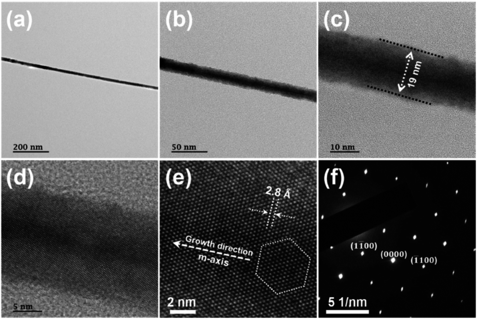 | ||
| Fig. 6 Transmission electron micrographs of GaN core NWs grown on a BeO substrate: (a–c) low- to high-magnification images, (d) high-magnification image showing planes with the complete width, (e) interplanar spacing along the m-axis with a very clear growth direction, and (f) SAED patterns verifying the growth direction along the m-axis. Reproduced with permission from ref. 81. Copyright 2020 ACS publisher. | ||
3.3 Growth of 1D GaN nanowires on graphene-coated monolayer Cu foil
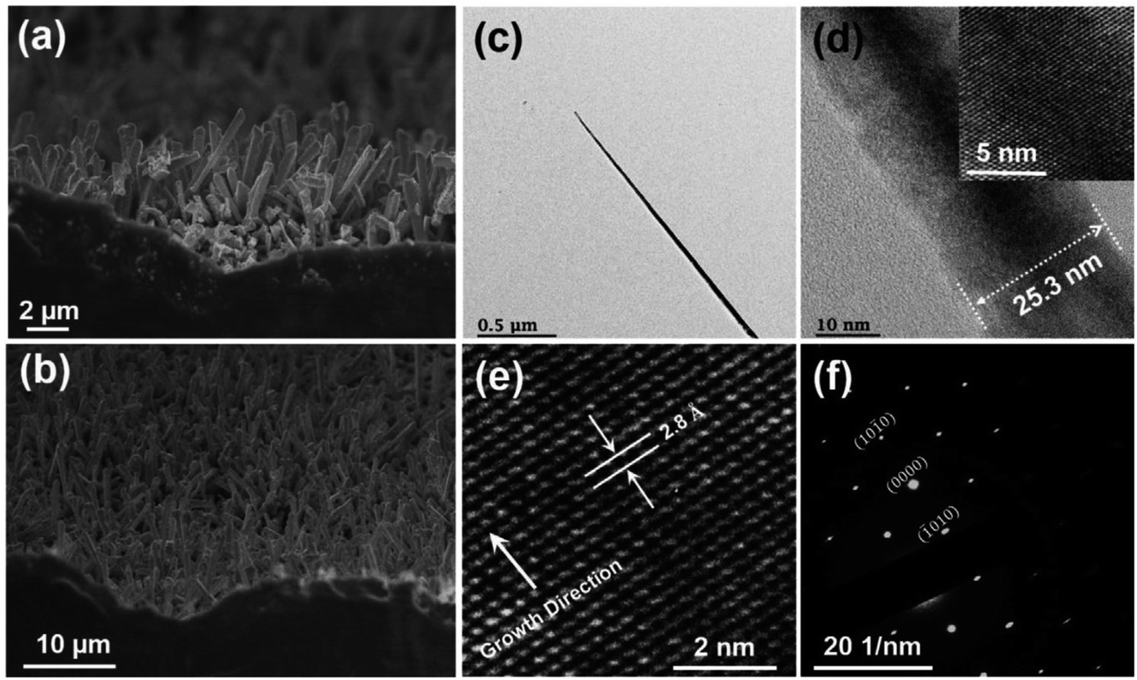
The van der Waals (vdW) heteroepitaxial growth method was used to grow single-crystal GaN NWs on a polycrystalline nature metallic substrate,55 as illustrated in Fig. 7(a). Due to the low melting temperature of the Cu substrate, the VLS method with Au as the major catalyst is used to develop GaN NWs at low temperatures. Low-melting-temperature metals such as In and Ga are used to further lower the melting temperature of the catalyst for agglomeration. Following agglomeration, the homogeneous alloy is created by annealing, resulting in a well-separated spherically shaped alloy catalyst. Fig. 7(b-i) and (b-ii) show a schematic of the agglomeration as well as the related SEM images. Because the substrate is metallic, Au/In/Ga can interact with Cu. However, the graphene covering on the Cu foil prevents any interaction or direct contact of the Au/In/Ga alloy with the Cu foil. Graphene had a covering area of more than 95%,82 and the graphene coating worked as a single-crystalline substrate. Furthermore, the use of a graphene covering is advantageous owing to graphene's extremely high electrical conductivity. As a result, a spherical Au/In/Ga metal-alloy catalyst formed on top of graphene. Following the delivery of the precursors, the catalyst absorbed Ga and nitrogen, and at supersaturation of the catalyst, the precursors began to precipitate at the substrate–catalyst interface. Fig. 7(c-i) depicts a schematic of the NW growth, which began at the substrate–catalyst interface and extended upward. Fig. 7(c-ii) and (c-iii) show the scanning electron micrographs of GaN NWs grown on Cu foil. The growth was then shifted from VLS to VS mode by raising the V/III ratio to 18![[thin space (1/6-em)]](https://www.rsc.org/images/entities/char_2009.gif) 000, and bird's-eye and top view SEM images are shown in Fig. 8(a) and (b).
000, and bird's-eye and top view SEM images are shown in Fig. 8(a) and (b).
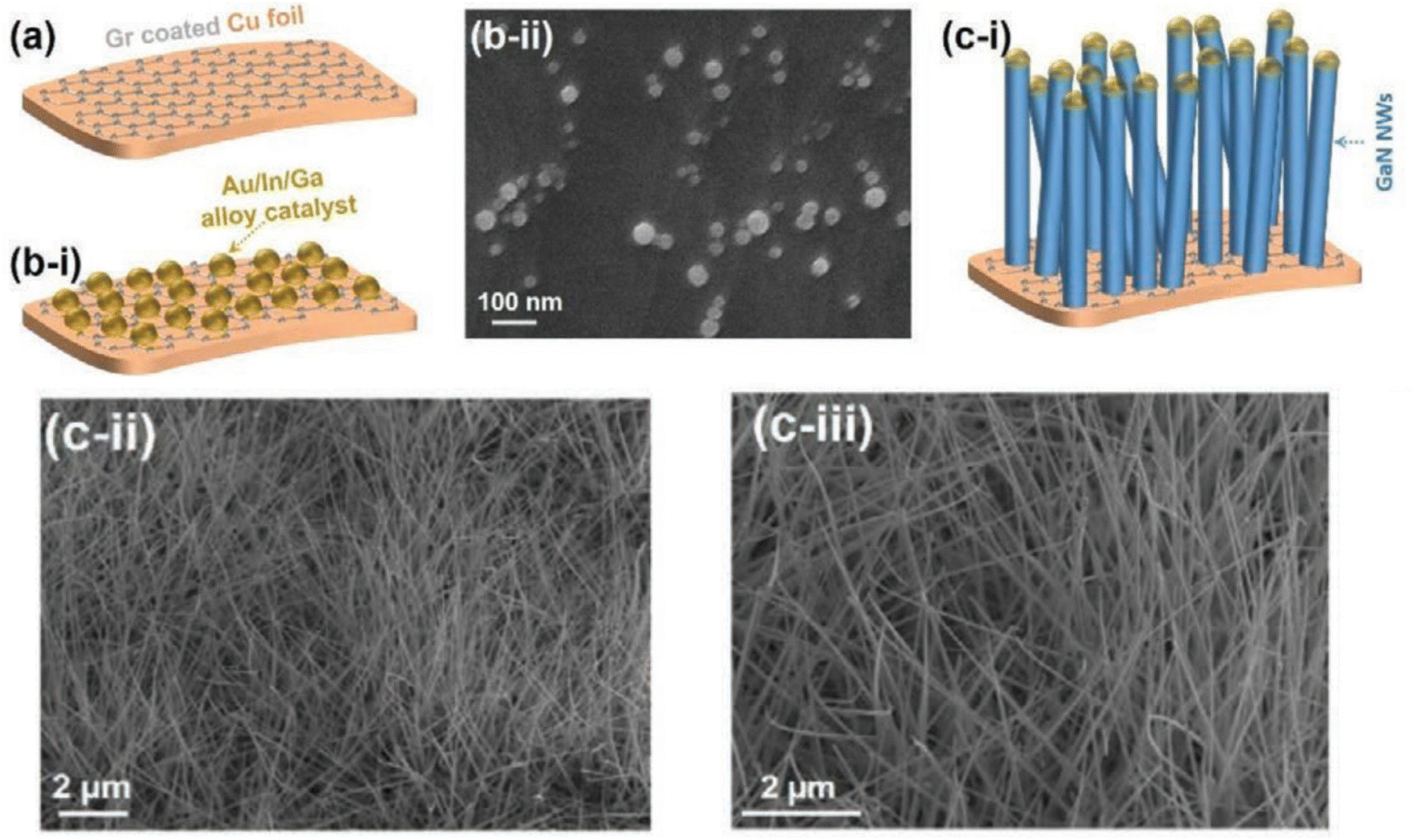 | ||
| Fig. 7 Growth of GaN NWs on a graphene-coated Cu foil. Illustration of: (a) a graphene-coated Cu metal foil and (b-i) Au/In/Ga metal-alloy catalyst aggregation. (b-ii) SEM micrograph of catalyst agglomeration. (c-i) GaN nanowires grown on a graphene-coated Cu foil, (c-ii) low-magnification SEM micrograph of GaN NWs, and (c-iii) high-magnification SEM micrograph of GaN NWs. Reproduced with permission from ref. 55. Copyright 2020 Wiley publisher. | ||
 | ||
| Fig. 8 (a) High-magnification and (b) low-magnification SEM images of GaN NWs following GaN shell growth. (c) A low-magnification TEM image of GaN core NWs, (d) a high-magnification image of the corresponding NW with an inset showing the planar order normal to the growth direction, (e) a very-high-magnification image depicting the interplanar spacing of 2.8 Å, and (f) SAED patterns confirming the growth direction along the m-axis. Reproduced with permission from ref. 55. Copyright 2020 Wiley publisher. | ||
TEM and SAED measurements are used to assess the crystal quality and growth direction of the GaN NWs. Fig. 8(c) and (d) shows a low and high-magnification image with a very smooth surface of the NWs and an inset showing smooth planes perpendicular to the growth direction. Interplanar spacing corresponds to the m-axial growth direction illustrated in Fig. 8(e). SAED patterns verified the growth direction, and the growth direction is confirmed to be the same as that observed from the interplanar spacing illustrated in Fig. 8(f). TEM measurements performed on many NWs depicts the NWs had the same size, shape, crystal quality, and growth direction. Finally, single crystalline GaN NWs can be grown on low melting temperature substrates using the VLS approach for a variety of applications.
3.4 Growth of 1D GaN HS on a glass substrate
A simple two-step VLS–VS growth method is used to grow highly crystalline m-axis GaN NWs on an amorphous glass substrate,83 as shown in Fig. 9(a)–(d). A metal alloy catalyst initiated the formation of high-quality GaN core NWs.84,85 The Au/In/Ga alloy catalyst solidly agglomerated by in situ annealing of the samples in an MOCVD reactor in an H2 environment to create well-separated nanoparticles with a diameter of 42 ± 10 nm, as illustrated in Fig. 9(g). High-aspect-ratio (∼62) NWs shown in Fig. 9(h) are formed by means of the VLS growth mode. The size of the metal alloy catalyst determines the diameter of the NWs. A low V/III ratio of 25 is a critical criterion for the axial growth of NWs. The GaN NWs have lengths of 3 ± 0.2 μm, diameters of 48 ± 10 nm, and densities of 8 ± 0.5 108 cm−2. Because it is widely known that the growth direction of GaN core NW can be modified by optimizing the supply of precursors,86 the growth direction is optimized utilizing a finely regulated supply of gallium and nitrogen precursors. Fig. 9(b) and (i) show the respective schematic and SEM image of the GaN NWs, respectively, following the conformal growth of GaN shells. A wetting layer can be detected at the nucleation site of the GaN NWs on the substrate, as shown in Fig. 9(i). Following the formation of the GaN shell, five pairs of InGaN/GaN triangular-shaped MQW shells were grown conformally utilizing the VS growth method. Triangular-shaped InGaN/GaN MQW shells surrounding the GaN NWs are depicted schematically in Fig. 9(c) and (d). Fig. 9(e) and (f) show images of the 2-inch glass substrates before and after the formation of the NWs, respectively. The low-magnification bird's-eye view SEM image of InGaN/GaN MQW coaxial NWs evenly grown on an amorphous glass substrate is shown in Fig. 9(j). In addition, a high-magnification image with an inset verifies the smooth surface of the NWs in Fig. 9(k). The top view low-magnification SEM image and the high-magnification inset in Fig. 9(i) reveal homogenous growth. It is evident that the growth on top of the glass substrate is homogeneous. Throughout the 2-inch substrate, the same growth morphology was observed. Furthermore, the growth quality was consistent from run to run and did not decline, indicating the wide growth window of Au-catalyzed GaN NWs on glass substrates by MOCVD.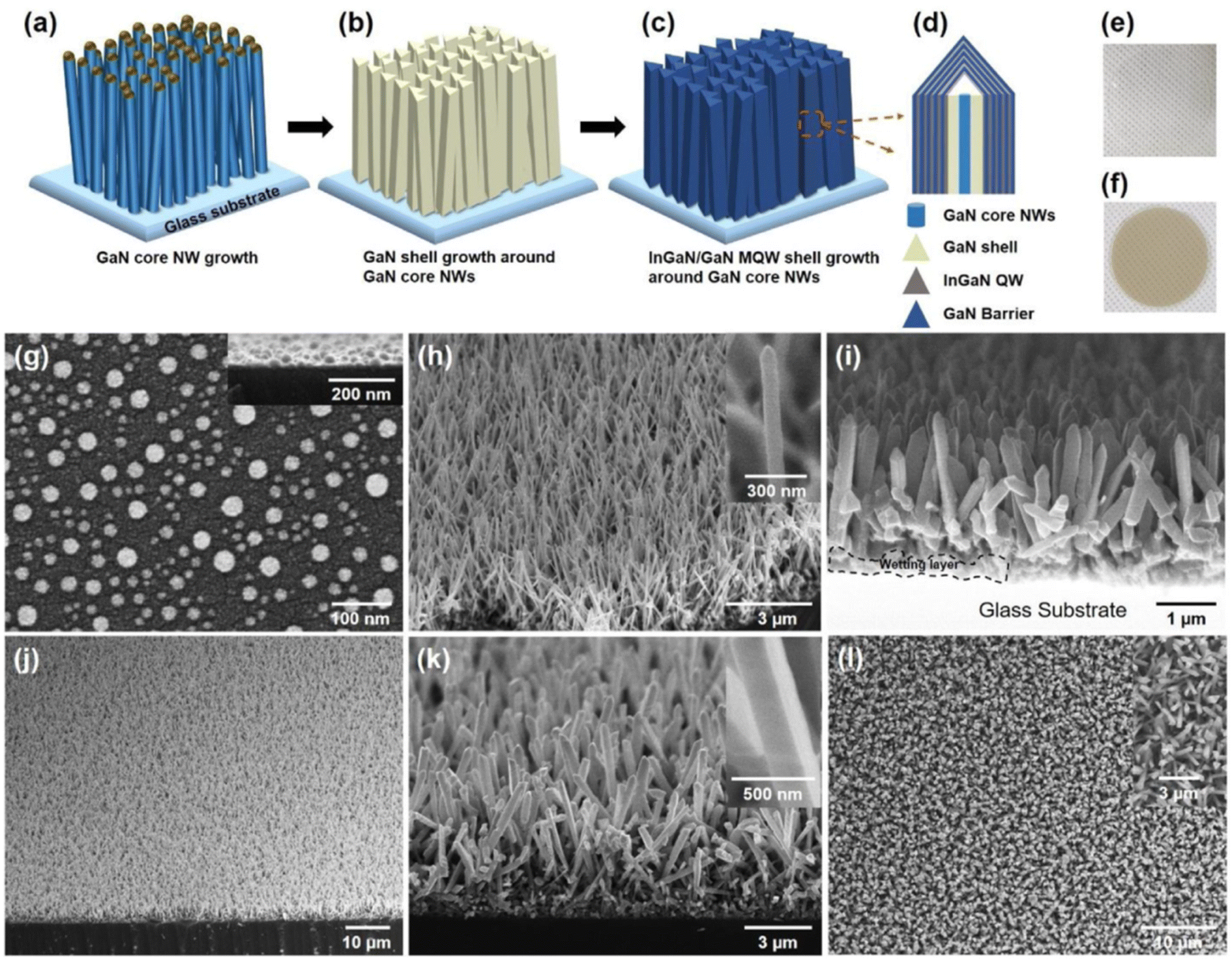 | ||
| Fig. 9 Schematic representation of the growth sequence of: (a) GaN core NWs by VLS, (b) triangular-shaped GaN shells enclosing GaN core NWs by VS mode, (c) InGaN/GaN triangular-shaped MQW shells around GaN shells, and (d) a bird's-eye view of the entire structure of GaN/InGaN MQW NW. Images of the glass substrate: (e) after Au deposition and (f) following GaN/InGaN MQW growth. Scanning electron micrographs of: (g) Au/In/Ga alloy catalyst agglomeration (inset shows side view), (h) GaN core NWs (inset shows a high-magnification view of a single NW), (i) GaN NWs following growth of GaN shell, (j) bird's-eye view of InGaN/GaN MQW NWs, (k) high-resolution image of InGaN/GaN MQW, and (l) top view of MQW NWs. Reproduced with permission from ref. 83. Copyright 2020 Elsevier publisher. | ||
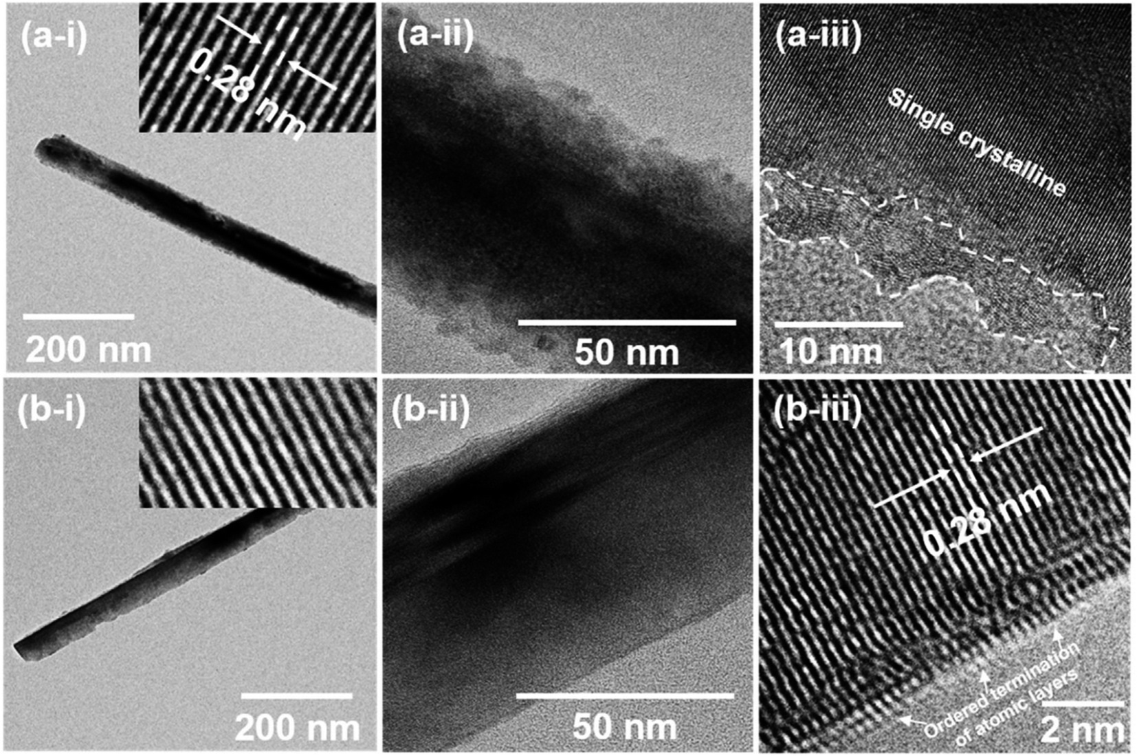
In situ post-growth annealing in an NH3 environment, known as nitridation, is used to smoothen the surface up to the atomic level. In this regard, Fig. 10 depicts two series of TEM images, namely series (a) and series (b). Fig. 10(a-i) and (a-ii) show TEM images of the NWs at low and high magnifications without post-growth nitridation, in which the surface is not smooth. The NWs have a triangular cross-section, and one of the edges is highlighted in Fig. 10(a-iii); the crystal planes of the edge are not aligned with the crystal planes of the inner part of the NW. Furthermore, the interplanar spacing of the lattice planes is 0.28 nm, as can be observed in the inset of Fig. 10(a-i). The interplanar space corresponds to the m-axial growth direction. The low and high magnification TEM images of the NWs after smoothening the edge of the triangular cross-section by adding the in situ post-growth nitridation process are shown in Fig. 10(b-i)–(b-iii). The images in Fig. 10(b-ii) and (b-iii) show high-magnification images focused on the lateral edge of a triangular NW, and the orderly termination of atomic layers is illustrated. The interatomic spacing is depicted in the inset of Fig. 10(b-i), and the measurement is depicted in Fig. 10(b-iii) with a value of 0.28 nm, which is ascribed to the core NWs' m-axial development direction. Thus, the TEM data show that the growth direction of the GaN core NWs is along the m-axis.
 | ||
| Fig. 10 Transmission electron micrographs of a GaN NW after GaN shell growth: (a-i and a-ii) low- and high-magnification images (inset of (a-i) shows the interplanar spacing), (a-iii) high-magnification image focused on the termination of the side planes of a GaN shell, (b-i and b-ii) low- and high-magnification images (inset of (b-i) shows the inter planner spacing) (b-iii) high-magnification image focusing on the termination of the GaN shell side planes with a very clean surface termination at the atomic level. Reproduced with permission from ref. 83. Copyright 2020 Elsevier publisher. | ||
After growing highly crystalline triangular-cross-section GaN shells around the m-axis GaN core NWs, five pairs of InGaN/GaN MQW shells are grown on sides of a triangle-shaped geometry, as shown schematically in Fig. 11(a). The cross-sectional view schematic is shown in Fig. 11(b), elucidating the growth facets of InGaN QW on the semipolar planes. Fig. 11(c) shows the TEM (HAADF-STEM) image of a full cross-sectional view of a NW. The inset displays a high-magnification image with an interplanar distance assigned to the c-plane; hence, the basal plane is (000 2). Fig. 11(d), (e) and (f) show high-resolution micrographs of the top cone, right side, and left side of the cross-sectional view, respectively. Between the InGaN QW and the GaN barrier, a very clear boundary can be observed. Fig. 11(g) depicts an InGaN QW thickness of 1.6 nm and a GaN barrier thickness of 10 nm. Fig. 11(h) shows the SAED patterns that were obtained with the zone axis of m-plane. An EDS line scan performed for the entire InGaN/GaN MQW structure to examine indium incorporation, and the scanned area is marked with a yellow line in Fig. 11(i); the variation in the gallium and indium elements over the measurement length is depicted in the overlapping graphs of Fig. 11(i). EDS elemental mapping to study the overall picture of indium incorporation in a wide range, and the laid-out image of indium, gallium, and nitrogen is shown in Fig. 11(j). The elemental mapping for indium, gallium, and nitrogen separately are shown in Fig. 11(k), (l) and (m), respectively. The TEM investigation revealed the formation of monocrystalline high-quality triangular-shaped InGaN/GaN MQW shells surrounding the GaN NWs. The above-mentioned growth procedures and characterizations lead to the conclusion that single crystalline GaN NWs can be synthesized on an amorphous substrate using the VLS methodology.
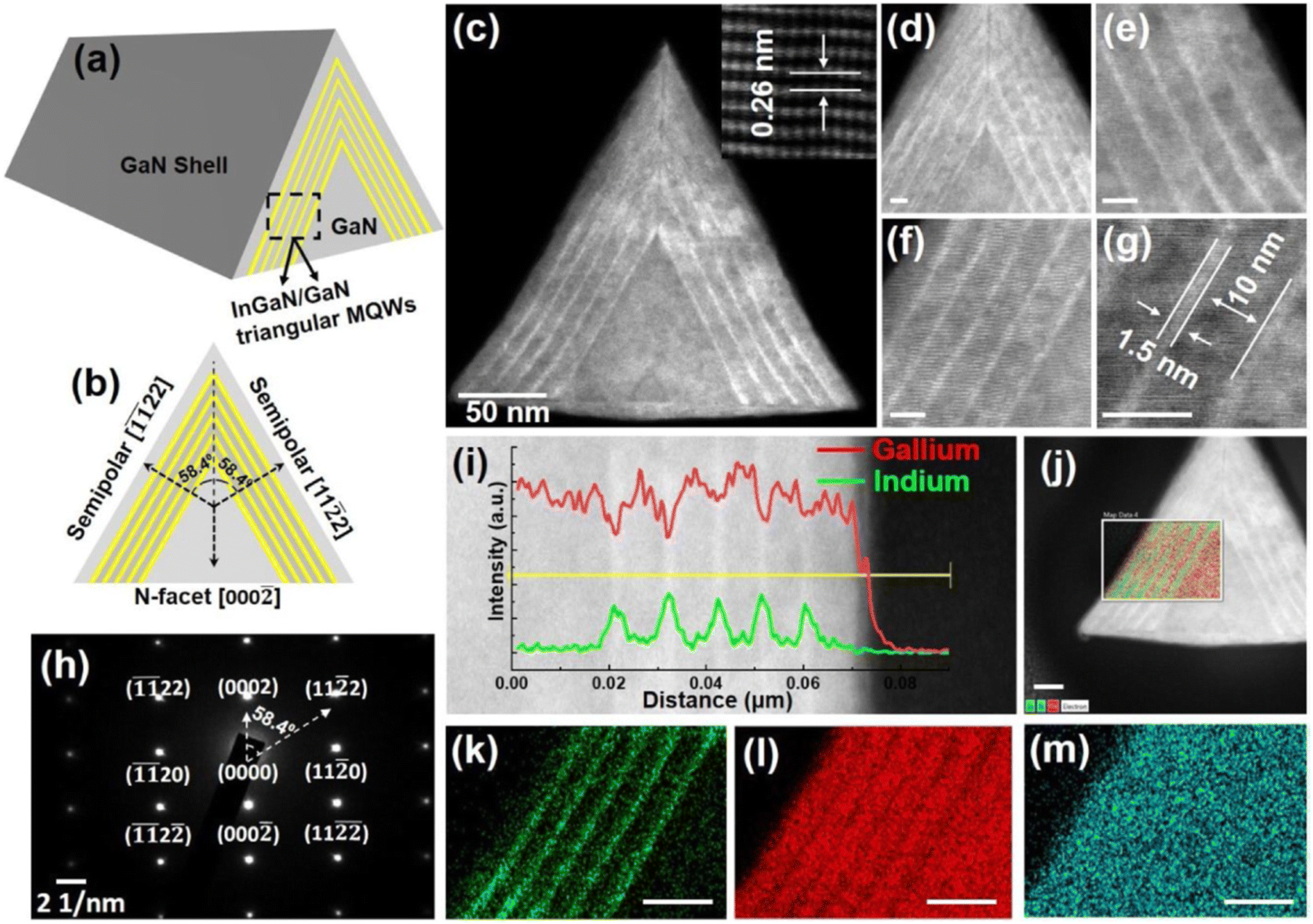 | ||
| Fig. 11 (a) Schematic of InGaN/GaN MQW triangular shells with side view of NWs; (b) cross-sectional view of InGaN/GaN MQW triangular shells with N-facet [000 ] orientation of basal plane and semipolar (112) planes. InGaN/GaN triangular-shaped MQW structural characterizations: (c) HAADF-STEM cross-sectional image of InGaN/GaN triangular-shaped MQW NW (inset shows atomic-resolved high-resolution STEM image showing interplanar spacing). High-magnification images of: (d) upper part, (e) right side, and (f) left side of the cross-section of InGaN/GaN MQW triangular shells. The scale bar for (d)–(g) is 10 m. (h) SAED patterns measured from the zone axis of the m-plane [1 100]. STEM EDS (i) line profile analysis/scan of InGaN/GaN MQW triangular-shaped shells (the stacked graphs show the composition of gallium and indium along the lateral direction of the cross-section as a function of distance). EDS elemental mapping of the whole structure: (j) gallium, indium, and nitrogen; (k) indium; (l) gallium; and (m) nitrogen. Reproduced with permission from ref. 83. Copyright 2020 Elsevier publisher. | ||
3.5 Growth of 1D GaN HS on GaN thin film
Pristine and coaxial GaN NWs on GaN thin film were grown by MOCVD. VLS and VS growth modes are utilized for the growth of core and shell, respectively.87 To create pure GaN NWs, 3 μm-thick c-plane GaN thin films (grown on sapphire) are utilized as the substrate, which was then coated with Au thin film. The Au-coated GaN substrates are placed into the MOCVD reactor for the VLS growth of core GaN NWs. The growth was conducted in an H2 atmosphere. The p-GaN shell was grown by injecting Cp2Mg for p-type doping and altering the growth mode from VLS to VS by increasing the V/III ratio. Fig. 12 depicts a schematic representation of the NW growth sequence.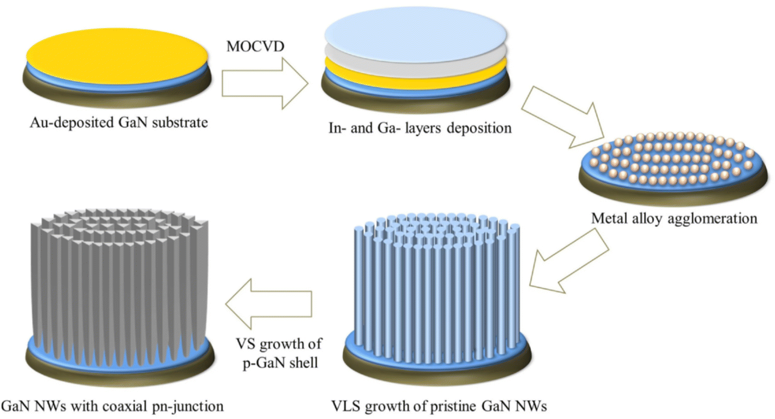 | ||
| Fig. 12 Growth schematics of pristine and coaxial GaN NWs on a GaN thin film. Reproduced with permission from ref. 87. Copyright 2021 Elsevier publisher. | ||
SEM characterization reveals the morphology of pristine and coaxial GaN NWs. Fig. 13 show the agglomeration of the well-separated spherical droplets of homogenous alloy catalyst. The formation of pure GaN NWs commenced after the agglomeration stage by injecting the precursors is shown in Fig. 13(c) and (d). Following the formation of pure GaN NWs, the p-GaN shell is epitaxially formed on the NWs, as illustrated in Fig. 13(e); the surface morphology of the NWs is shown by magnified image in Fig. 13(f). The tip of the coaxial NW has a trigonal pyramidal form, as can be observed in the inset of Fig. 13(f).
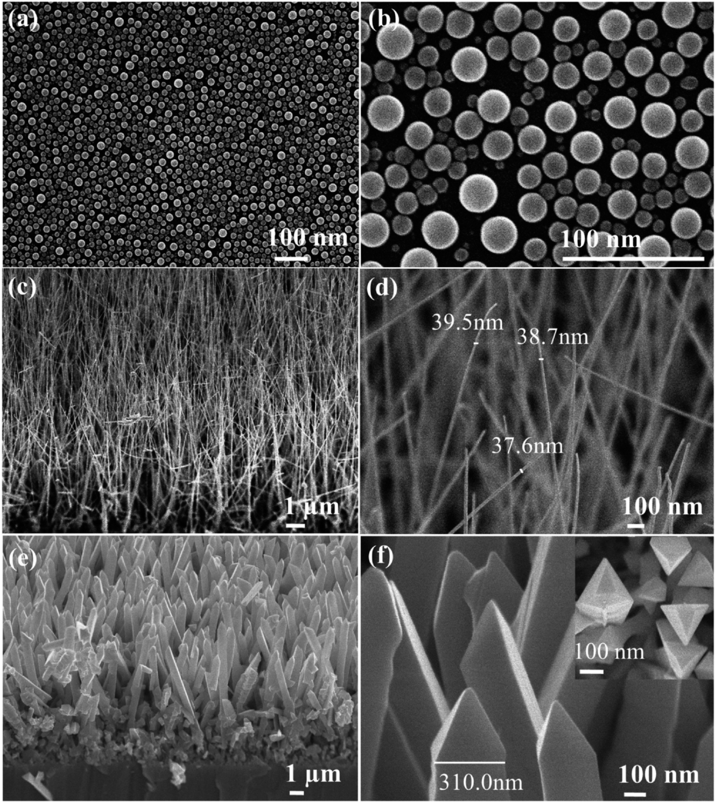 | ||
| Fig. 13 (a and b) SEM images of agglomerated Ga–In–Au alloy at different scales. (c and d) SEM photos of pristine GaN NWs at different scales. (e and f) SEM images of p–n junction coaxial GaN NWs at different scales. Reproduced with permission from ref. 87. Copyright 2021 Elsevier publisher. | ||
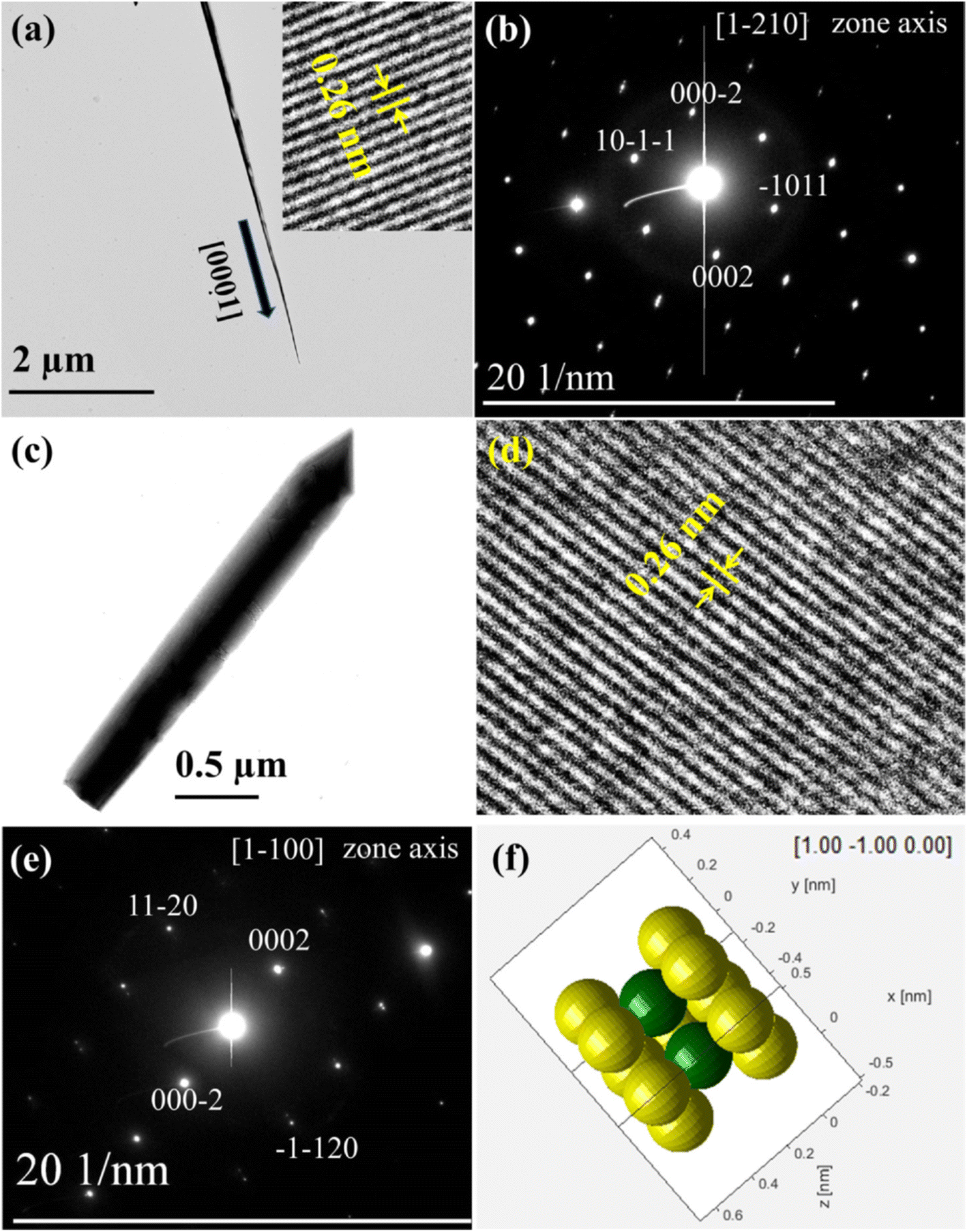
The crystallographic orientation of the pristine and coaxial GaN NWs is validated by TEM characterization. TEM images of a single pure GaN NW and its enlarged lattice fringes (inset of Fig. 14(a)) indicate a D-spacing of 0.26 nm, which is consistent with c-axis GaN NWs. It is proven by SAED pattern (taken along the [110] zone axis) that the GaN NW grows along the c-axis (Fig. 14(b)). Similarly, Fig. 14(c) depicts a TEM image of a single coaxial GaN NW with a triangular cross-section; its enlarged lattice fringes validate the 0.26 nm D-spacing (Fig. 14(d)). The SAED pattern (taken along the [100] zone axis) shown in Fig. 14(e) demonstrates that the crystallographic orientation of the GaN coaxial NW is along the c-axis. The SAED diffraction pattern of the coaxial NW identifies a wurtzite crystal structure orientated along the c-axis (Fig. 14(f)). According to the TEM results, pristine and coaxial GaN NWs formed along the c-axis. Characterization results demonstrate that GaN NWs with good crystal quality can be effectively grown on GaN thin films using the VLS approach for a variety of applications such as energy conversion and LED.
 | ||
| Fig. 14 (a) TEM image of pristine GaN NWs, in which inset shows magnified lattice fringes, (b) SAED pattern of pristine GaN NWs, (c) TEM image of coaxial GaN NW, (d) magnified fringes of a coaxial GaN NW, (e) SAED pattern of coaxial GaN NWs, and (f) model of wurtzite GaN crystal structure oriented along the c-axis. Reproduced with permission from ref. 87. Copyright 2021 Elsevier publisher. | ||
4. Applications of 1D GaN-based heterostructures
Because of their excellent mechanical characteristics, structural perfection due to their defect-free structure, improved strain confinement, high elastic limit of deformation without plastic deformation, high radiative recombination rate, strong electron mobility, variable energy band gap ranging from near-infrared (InN, 0.64 eV) to ultraviolet (AlN, 6.2 eV), increase in reactive surface area, and improved charge separation, GaN NWs are the most attractive choices for piezoelectric nanogenerators (PENGs),88 light-emitting diodes (LEDs),89 and solar-driven water splitting.904.1 Piezoelectric properties of 1D GaN-based heterostructures
In recent years, ambient energy harvesting technologies for powering wearable electronics, multipurpose portable electronic devices, and implantable devices have advanced rapidly. One of the most significant methods for harvesting the energy of microscale ambient mechanical sources is the conversion of mechanical energy into electrical energy utilizing PENGs.91–93 Ambient actuation sources such as vibrations, bending, vehicle movement, air flow, fluid flow, muscle action, running, and walking are the most prevalent actuation sources for PENGs among the various energy sources in nature.94,95GaN has a non-centrosymmetric crystal structure, which implies that when stressed, the centers of the cations and anions become out of balance, causing a tiny dipole moment in each unit cell, and the superposition of such dipole moments results in a piezoelectric potential throughout GaN.55
Fig. 15(a) represents a schematic of the device fabrication after it was hardened by annealing at 120 °C for 40 min. The NWs grown on the Cu foil are implanted in PDMS by covering the top of the device with PDMS, as illustrated in Fig. 15(b), and the image of the matching device is shown in Fig. 15(c). Finally, the top and bottom contacts are made, as indicated schematically in Fig. 15(d).
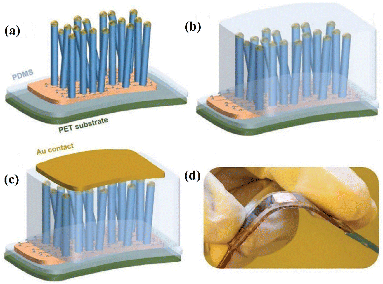 | ||
| Fig. 15 (a) Transfer of GaN NWs grown on a graphene-coated Cu foil onto a PDMS-coated PET substrate. (b) PDMS deposition to build a GaN NW-PDMS matrix on the substrate. (c) Au evaporation onto the PENG. (d) Image of the full device's corresponding structure. Reproduced with permission from ref. 55. Copyright 2020 Wiley publisher. | ||
By bending the PENG with a cyclic stretching-releasing agitation mechanism powered by a linear motor, the piezoelectric output is investigated. The arrangement includes a fixed plate and a moving plate, and the PENG is attached to the plates by sandwiching it between the plates, as illustrated in Fig. 16(a-ii). Fig. 16(a-i) depicts the bending, whereas Fig. 16(a-ii) shows the photograph of the arrangement. As the sliding plate moves forward, the PENG begins to bend, as indicated in the schematic in Fig. 16(b-i), and the bending phases are depicted in the images of Fig. 16(b-ii) and (b-iii). A detailed cross-sectional drawing of the PENG is shown in Fig. 16(c) to illustrate the stress distribution in the active media of the PENG owing to bending. The PENG faces compressive stress at the bottom and tensile tension at the top as it bends. Because the NWs matrix is embedded in the top half of the device, NWs encounter tensile stress laterally, resulting in the formation of radial compressive stress, as seen in Fig. 16(d). As a result, the bending angle specifies the PENG's degree of strain. Fig. 4(d) shows a NW with no stress on the left and a NW with compressive stress due to bending on the right. The piezoelectric output voltage is 19.7 volts, as shown in Fig. 16(e), with an inset of a magnified image of the output waveform. Fig. 16(f)–(h) show the piezoelectric output current measured at various bending angles, and it can be observed that the degree of bending impacts the magnitude of the stress encountered by the PENG. The current output ranged from 30 mA cm−2 to 1.97 mA cm−2 while the actuation frequency was kept constant at 8 Hz for both the chronoamperometry and chronopotentiometry studies. Over 4 million cycles stability test showed no substantial deterioration in the performance of the device. Based on the results obtained from PENG fabricated using GaN NWs, it is inferred that abundant electrical energy might be harvested by employing GaN NWs for the construction of PENGs.
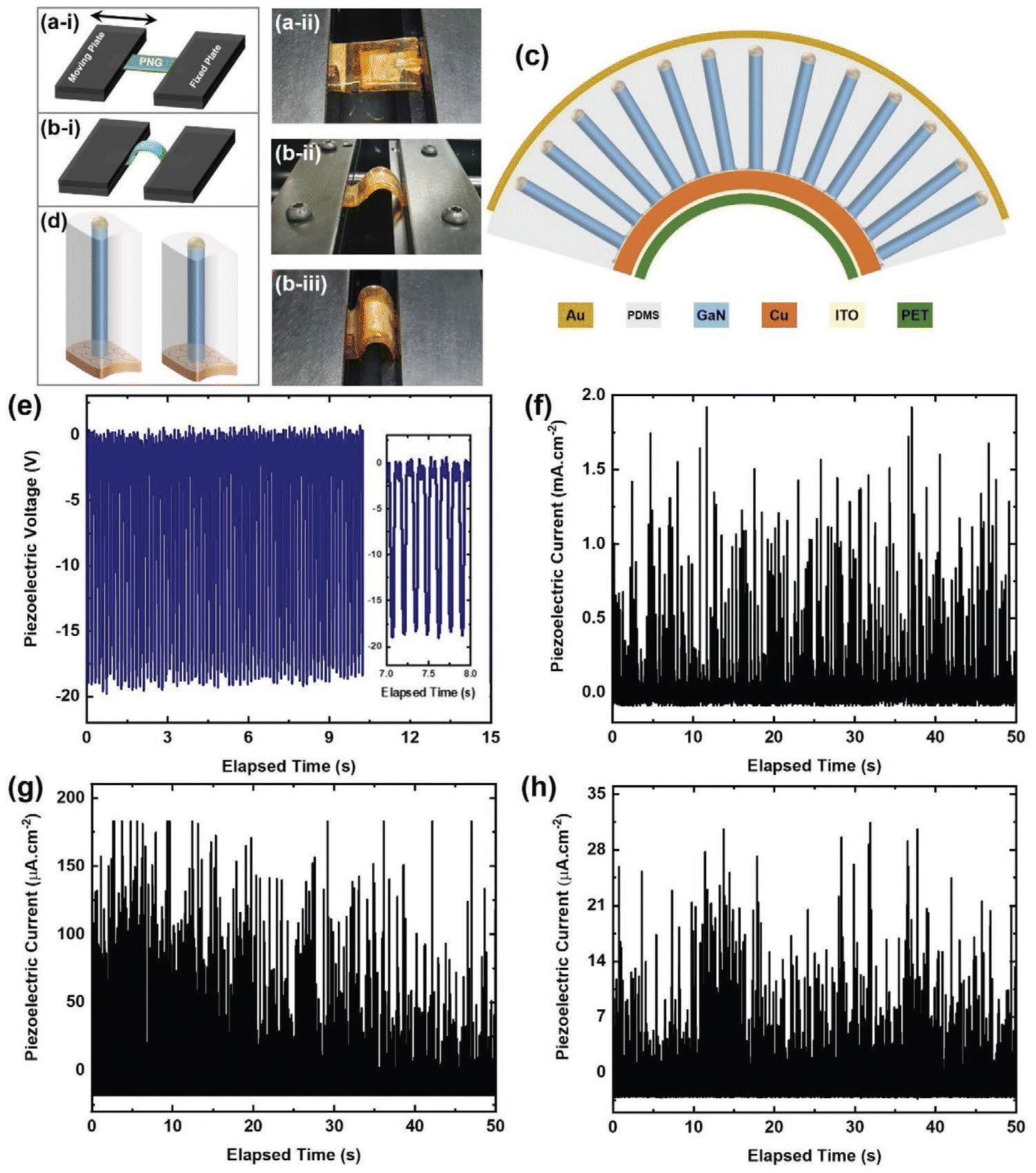 | ||
| Fig. 16 (a-i) Schematic illustration of the cyclic stretching-releasing agitation setup when the PENG is not bent, (a-ii) photograph of the PENG in the same configuration, (b-i) schematic illustration of the agitation setup when bent, (b-ii) photograph of the setup as bending begins, and (b-iii) photograph of the setup when full bending is achieved. (c) Schematic illustration of the NWs undergoing tensile stress applied laterally upon bending of the PENG, (d) demonstration of the NWs' lateral tensile stress being converted into compressive axial stress, (e) piezoelectric output voltages, piezoelectric output current upon: (f) maximum bending, (g) medium bending, and (h) minor bending. Reproduced with permission from ref. 55. Copyright 2020 Wiley publisher. | ||
4.2 Light-emitting properties of 1D GaN-based heterostructures
The III-nitride semiconductor-based epitaxial nanowires (NWs) demonstrate novel properties such as a high radiative recombination rate, a small Auger effect, high electron mobility, and a variable energy band gap ranging from near infrared to ultraviolet. Because of these properties, III-nitride NWs may be considered a possible contender for LED applications.83,96,97Fig. 17 shows an electrically driven InGaN/GaN QD-QW NW-based hybrid LED. A p-GaN shell grown with a reduced growth rate to cover NWs conformally, followed by a high growth rate to accomplish the coalescence of p-GaN solely around the top of the NWs for the electrical pumping of carriers. Fig. 7(a) and (b) show the schematic drawing and SEM micrograph of the whole structure. Because of the different rotational orientations of the m-plane NWs, the coalesced p-GaN has a polycrystalline morphology; nonetheless, we believe that this has no effect on LED functioning. The device's light-emitting efficiency is principally governed by the single-crystalline and defect-free InGaN/GaN MQWs. The role of p-GaN is to transfer holes to the active layer, and it is independent of the GaN quality. The bottom wetting layer is utilized to pump electrons into the active area; however, due to its thinness, it cannot tolerate extremely strong current injection. The p-type contacts consisted of Ni/Au, and the n-type contacts are soldered with an indium bottom wetting layer. Fig. 7(c) depicts the current–voltage curve with an inset image of the LED. Interestingly, a p–n junction is developed on a c-lateral facet with no QWs that could result in source loss, although the loss should be extremely modest owing to the very thin p-GaN layer on the c-lateral facet due to the very low growth rate of the c-lateral facet compared with that of semipolar facets. As a result, for the first time, Johar et al. demonstrated LED operation using conformally grown triangular-shaped InGaN/GaN MQW NWs, which have low dimensions, suppressed QCSE, excellent IQE, and an ultrashort carrier lifetime. It is concluded that GaN NWs have ample potential for the fabrication of LEDs utilizing different kinds of nanostructures on various substrates.
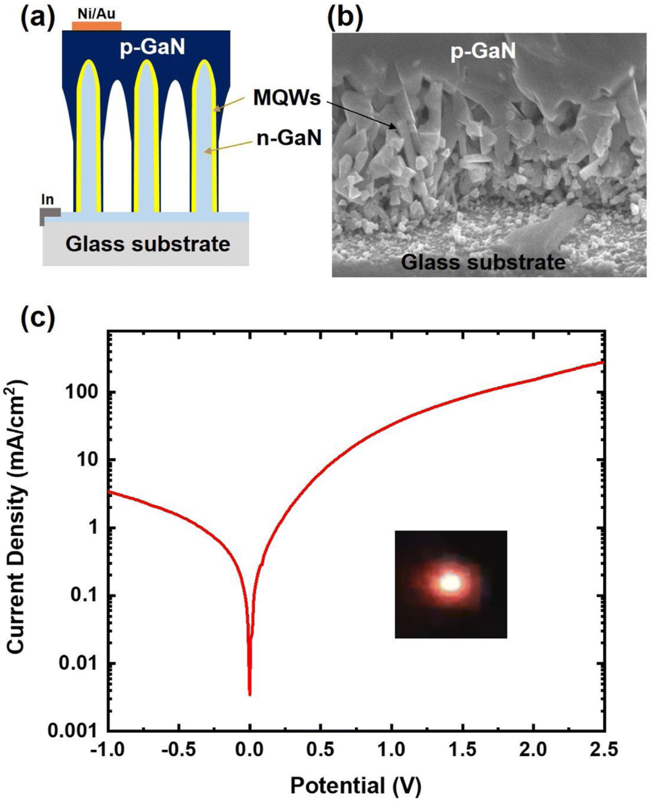 | ||
| Fig. 17 (a) Schematic representation of the whole structure of a NW-based LED, (b) SEM micrograph of the developed structure, and (c) LED IV measurement (inset shows an image of an LED). Reproduced with permission from ref. 83. Copyright 2020 Elsevier publisher. | ||
4.3 PEC water-splitting properties of 1D GaN-based heterostructures
Global energy consumption is quickly expanding, and reliance on nonrenewable energy supplies is quickly increasing CO2 content in the atmosphere, resulting in global warming. Renewable energy resources have piqued the interest of experts all around the world to address this issue. Hydrogen has the potential to be a viable alternative energy source since it is ecologically benign, has a high energy density, and can be created from a large amount of water and solar energy. The photoelectrochemical (PEC) technique for splitting water is a potential approach for creating hydrogen from water and solar energy.98–100Metal nitrides have received much interest due to their structural stability and electrical conductivity, and III–V semiconductors have emerged as a viable option for PEC water splitting. The defining qualities that make III–V semiconductors attractive candidates for PEC water splitting include band gap tunability, prolonged carrier lifetime, and improved crystal quality. GaN is a III–V semiconductor with a straight band gap and conduction and valence bands that span the water redox level; hence, no external bias is required.52,101,102 There are several strategies to enhance PEC water splitting. Nano-structuring is one of the key strategies to significantly improve PEC water splitting. In recent years, 1D nanostructures have been extensively explored for PEC water splitting. In 1D nanostructures, lattice-incompatibility limitations are relaxed, leading to decreased dislocation development and a low piezoelectric polarization field. In addition, 1D nanostructures increase the reactive surface area and improve charge separation.103–105 When a semiconductor comes into contact with an electrolyte, effective charge transport via the interface is crucial. Passivation/overlayers enhance the charge transfer rates by providing a convenient path for charge transfer from active sites, lowering surface state density, and limiting chemical corrosion.
Fig. 18 depicts the results of the PEC water-splitting measurements for GNWs/ZnS photoanodes. The photocurrent density is determined using linear scanning voltammetry (LSV), and the findings are displayed in Fig. 18(a). LSV measurements for samples with varying ZnS shell thicknesses reveal that holes transport effectively from the valence band of the GaN core material to the electrolyte via the ZnS overlayer for optimum ZnS shell thickness. At zero applied bias, Fig. 18(b) shows the dependency of photocurrent density on the thickness of the ZnS shell on the GaN core NW. The optimal sample's applied bias photon-to-current conversion efficiency (ABPE%) value was 1.12%, which is a meaningful value for a GaN-based photoanode. The ZnS overlayer inhibited surface and bulk recombination of photogenerated electron–hole pairs.
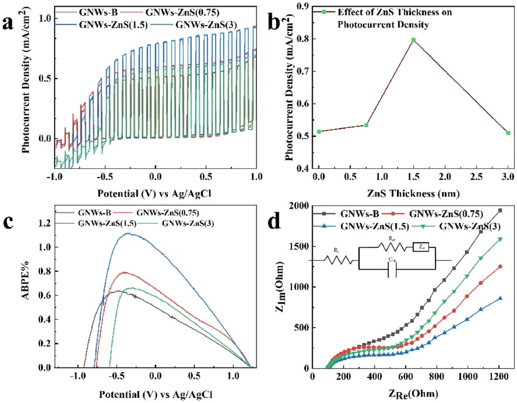 | ||
| Fig. 18 PEC water-splitting performance of bare and GNWs with various ZnS overlayer thicknesses. (a) LSV curves, (b) photocurrent density against ZnS overlayer thickness at zero bias under one-sun illumination, (c) ABPE%, and (d) EIS spectra. Reproduced with permission from ref. 90. Copyright 2022 Elsevier publisher. | ||
The electrochemical impedance spectra (EIS) of GNW photoanodes with varying thicknesses of the ZnS overlayer are shown in Fig. 18(d). The analogous circuit for the EIS spectra is shown in the inset. Each spectrum's semicircle represents the charge transfer resistance between the electrodes and electrolyte. Because ZnS stimulates the injection of photogenerated holes into the electrolyte from the core GNW for the oxidation reaction, GNW–ZnS (1.5) has the smallest-radius semicircle, implying low charge transfer resistance.
Furthermore, Au NPs sandwiched between the core GNW and the ZnS overlayer improve the PEC water-splitting performance of GNWs. Fig. 19 shows the ternary sandwiched nanostructure's PEC water-splitting properties. Under one-sun illumination at zero bias versus the Ag/AgCl reference electrode, the ternary sandwiched nanostructure showed a photocurrent density of 1.15 mA cm−2. Chronoamperometry results are used to evaluate the photostability of the ternary sandwiched nanostructure photoanode. As shown in Fig. 5(b), the ternary sandwiched nanostructure photoanode retained 76% of its initial PEC over a lengthy period (∼14 h), whereas bare GNWs retained 65% after a short (2.2 h) stability test. The suppression of bulk and surface recombination of photogenerated charges, as well as the ease of transporting them from the core GaN NW and Au NPs to the electrolyte via the ZnS overlayer, are the reasons for this increased stability.
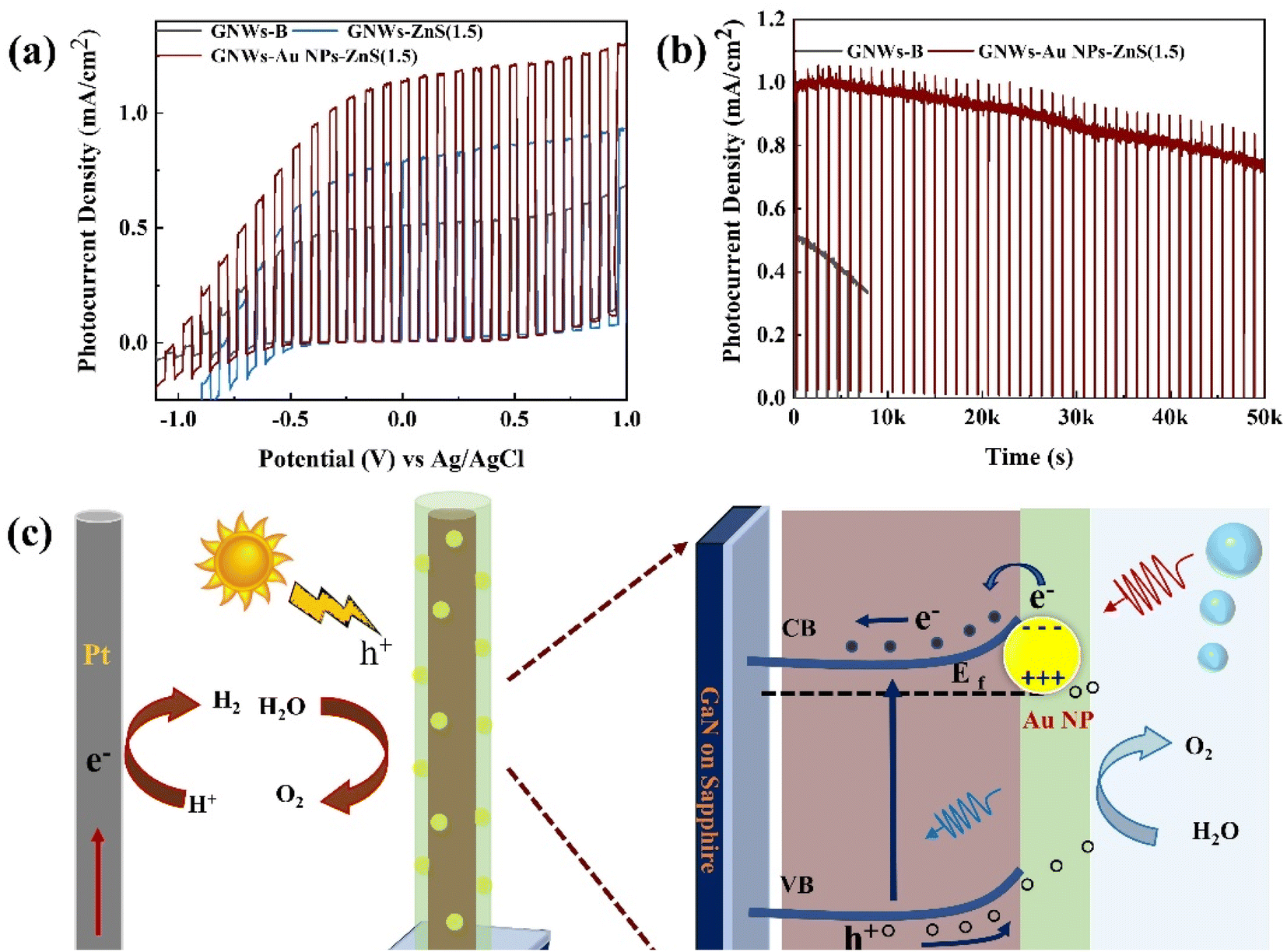 | ||
| Fig. 19 (a) LSV plots of a ternary sandwiched nanostructure photoanode, (b) chronoamperometry measurements at zero bias for comparing the stability of bare GNWs and ternary photoanodes, and (c) schematic depiction of the proposed mechanism for increased water-splitting efficiency of the ZnS/Au NPs/GNWs photoanode. Reproduced with permission from ref. 90. Copyright 2022 Elsevier publisher. | ||
The mechanism behind the significant increase in the PEC water-splitting performance for the ternary sandwiched nanostructure photoanode is presented in Fig. 19. Photogenerated electrons and holes are stimulated into the conduction and valence bands of GaN when exposed to light. Due to the existence of defects, bare GNWs have a high rate of electron–hole recombination on the surface, dramatically limiting the PEC water-splitting efficiency. The addition of a ZnS overlayer on the GNWs inhibits the recombination of photogenerated charges on the surface of the NW and speeds up the injection of photogenerated holes into the electrolyte for the PEC water oxidation process. The photoanode/electrolyte interfaces generated by the Au NPs and the ZnS passivation layer contribute to the improved PEC water-splitting performance of the ZnS/Au NPs/GNW photoanode. This signifies that the multi-interface fabrication strategy paves the way for the emergence of high-performance semiconductor photoelectrodes for efficient solar energy conversion. GaN NWs emerge as a strong candidate for PEC water splitting. The growth of single crystalline NWs using the VLS method on different conductive substrates is another great opportunity to enhance the usage of NWs in this horizon. Nanostructures of multiple shapes and sizes can be effectively utilized in PEC water splitting. The synthesis of shell/core structure can aid in the improvement of light harvesting, charge generation, and separation. Hence, it can be stated that GaN NWs grown using the VLS method on various substrates have proved as an excellent choice for energy conversion and LED applications.
5. Conclusions
This study provides a detailed explanation of the synthesis of GaN NWs using the VLS approach, as well as the growth of related heterostructures using MOCVD. The impact of the hosting substrate type on the morphology of NWs is explored as one of the various parameters that determine the morphology and crystal quality of GaN NWs. The shape, size, orientation, and crystal quality of 1D GaN-based HS are described using morphological and structural characterization. In PEC water splitting, piezoelectric nanogenerators, and light-emitting diodes, the performance of 1D GaN-based HS is investigated. According to the findings, the production of HS via the VS approach improved the performance of bare GaN NWs in all of the aforementioned applications.Conflicts of interest
The authors declare that they have no known competing financial interests or personal relationships that could have appeared to influence the work reported in this paper.Acknowledgements
This work was supported by the National Research Foundation of Korea (NRF), funded by the Ministry of Education, Science, and Technology (2018R1A6A1A03024334, NRF-2019R1A2C1006360). In addition, this research was supported by Basic Science Research Capacity Enhancement Project through Korea Basic Science Institute (National Research Facilities and Equipment Center) grant funded by the Ministry of Education. (Grant No. 2019R1A6C1010024).References
- Y. Zhong, et al., A review on the GaN-on-Si power electronic devices, Fundam. Res., 2022, 2, 462–475 CrossRef CAS.
- C.-T. Ma and Z.-H. Gu, Review on Driving Circuits for Wide-Bandgap Semiconductor Switching Devices for Mid- to High-Power Applications, Micromachines, 2021, 12, 65 CrossRef PubMed.
- GaN vs. SiC: Silicon Carbide and Gallium Nitride Compared, Arrow.com https://www.arrow.com/en/research-and-events/articles/silicon-carbide-and-gallium-nitride-compared Search PubMed.
- Advantages of Using Gallium Nitride Over Silicon Technology, Kensington, https://www.kensington.com/news/docking-connectivity-blog/5-reasons-why-you-should-make-the-switch-to-gallium-nitride-gan-over-silicon-devices/ Search PubMed.
- Gallium Nitride Semiconductor Devices Market Report, 2030, https://www.grandviewresearch.com/industry-analysis/gan-gallium-nitride-semiconductor-devices-market Search PubMed.
- T. Ueda, GaN power devices: current status and future challenges, Jpn. J. Appl. Phys., 2019, 58, SC0804 CrossRef CAS.
- T. Boles, GaN-on-Silicon – Present capabilities and future directions, AIP Conf. Proc., 2018, 1934, 020001 CrossRef.
- H. Ishida, et al., GaN-based semiconductor devices for future power switching systems, in 2016 IEEE International Electron Devices Meeting (IEDM), 2016, pp. 20.4.1–20.4.4, DOI:10.1109/IEDM.2016.7838460.
- A. Kravtsov, Development of silicon growth techniques from melt with surface heating, IOP Conf. Ser.: Mater. Sci. Eng., 2018, 355, 012007 CrossRef.
- K. Fujiwara, H. Koizumi, K. Nozawa and S. Uda, Crystal Growth Mechanisms of Silicon During Melt Growth Processes, 2012, DOI:10.7567/SSDM.2012.H-2-1.
- H. J. Jeon, J. H. Park, V. Artemyev and J. H. Jung, Melt-Crystal Interface Shape Formation by Crystal Growth Rate and Defect Optimization in Single Crystal Silicon Ingot, Current Photovoltaic Research, 2020, 8, 17–26 Search PubMed.
- T. Li, et al., Understanding the Growth Mechanism of GaN Epitaxial Layers on Mechanically Exfoliated Graphite, Nanoscale Res. Lett., 2018, 13, 130 CrossRef PubMed.
- R. Kucharski, T. Sochacki, B. Lucznik and M. Bockowski, Growth of bulk GaN crystals, J. Appl. Phys., 2020, 128, 050902 CrossRef CAS.
- J.-H. Lee and K.-S. Im, Growth of High Quality GaN on Si (111) Substrate by Using Two-Step Growth Method for Vertical Power Devices Application, Crystals, 2021, 11, 234 CrossRef CAS.
- M. Bockowski, et al., Growth of GaN on patterned GaN/sapphire substrates with various metallic masks by high pressure solution method, Proc. SPIE, 2006, 6121, 612103 CrossRef.
- C. F. Lin, et al., Growth and characterizations of GaN on SiC substrates with buffer layers, J. Appl. Phys., 1997, 82, 2378–2382 CrossRef CAS.
- W. A. Melton and J. I. Pankove, GaN growth on sapphire, J. Cryst. Growth, 1997, 178, 168–173 CrossRef CAS.
- W. Gian, M. Skowronski and G. S. Rohrer, Structural Defects and Their Relationship to Nucleation of Gan Thin Films, MRS Online Proc. Libr., 1996, 423, 475–486 CrossRef.
- C. Kisielowski, et al., Strain-related phenomena in GaN thin films, Phys. Rev. B: Condens. Matter Mater. Phys., 1996, 54, 17745–17753 CrossRef CAS PubMed.
- B. N. Sverdlov, G. A. Martin, H. Morkoç and D. J. Smith, Formation of threading defects in GaN wurtzite films grown on nonisomorphic substrates, Appl. Phys. Lett., 1995, 67, 2063–2065 CrossRef CAS.
- M. Bockowski, et al., Challenges and future perspectives in HVPE-GaN growth on ammonothermal GaN seeds, Semicond. Sci. Technol., 2016, 31, 093002 CrossRef.
- M. Bockowski, High nitrogen pressure solution growth of GaN, Jpn. J. Appl. Phys., 2014, 53, 100203 CrossRef.
- P. Von Dollen, S. Pimputkar, M. A. Alreesh, S. Nakamura and J. S. Speck, A new system for sodium flux growth of bulk GaN. Part II: in situ investigation of growth processes, J. Cryst. Growth, 2016, 456, 67–72 CrossRef CAS.
- A. Yoshikawa, E. Ohshima, T. Fukuda, H. Tsuji and K. Oshima, Crystal growth of GaN by ammonothermal method, J. Cryst. Growth, 2004, 260, 67–72 CrossRef CAS.
- M. Belousov, B. Volf, J. C. Ramer, E. A. Armour and A. Gurary, In situ metrology advances in MOCVD growth of GaN-based materials, J. Cryst. Growth, 2004, 272, 94–99 CrossRef CAS.
- B. Zhang and Y. Liu, A review of GaN-based optoelectronic devices on silicon substrate, Chin. Sci. Bull., 2014, 59, 1251–1275 CrossRef CAS.
- N. M. Lin, et al., GaN-Based LEDs With Air Voids Prepared by One-Step MOCVD Growth, J. Lightwave Technol., 2011, 29, 2831–2835 CAS.
- G. Li, et al., GaN-based light-emitting diodes on various substrates: a critical review, Rep. Prog. Phys., 2016, 79, 056501 CrossRef PubMed.
- H. Morkoç, A. Botchkarev, A. Salvador and B. Sverdlov, GaN based III–V nitrides by molecular beam epitaxy, J. Cryst. Growth, 1995, 150, 887–891 CrossRef.
- T. Sasaki and S. Zembutsu, Substrate-orientation dependence of GaN single-crystal films grown by metalorganic vapor-phase epitaxy, J. Appl. Phys., 1987, 61, 2533–2540 CrossRef CAS.
- J. N. Kuznia, M. A. Khan, D. T. Olson, R. Kaplan and J. Freitas, Influence of buffer layers on the deposition of high quality single crystal GaN over sapphire substrates, J. Appl. Phys., 1993, 73, 4700–4702 CrossRef CAS.
- F. A. Ponce, Defects and Interfaces in GaN Epitaxy, MRS Bull., 1997, 22, 51–57 CrossRef CAS.
- C. T. Foxon, et al., Homo- and Hetero-Epitaxial Gallium Nitride Grown by Molecular Beam Epitaxy, MRS Internet J. Nitride Semicond. Res., 1999, 4, 484–489 CrossRef.
- J. H. Choi, et al., Heteroepitaxial Growth of GaN on Unconventional Templates and Layer-Transfer Techniques for Large-Area, Flexible/Stretchable Light-Emitting Diodes, Adv. Opt. Mater., 2016, 4, 505–521 CrossRef CAS.
- R. R. Sumathi, Review—Status and Challenges in Hetero-epitaxial Growth Approach for Large Diameter AlN Single Crystalline Substrates, ECS J. Solid State Sci. Technol., 2021, 10, 035001 CrossRef CAS.
- A. Dadgar and A. Krost, Epitaxial growth and benefits of GaN on silicon, in III-Nitride Semiconductors and Their Modern Devices, ed. B. Gil, Oxford University Press, 2013, DOI:10.1093/acprof:oso/9780199681723.003.0003.
- J. Dong, L. Zhang, X. Dai and F. Ding, The epitaxy of 2D materials growth, Nat. Commun., 2020, 11, 5862 CrossRef CAS PubMed.
- J.-S. Park, M. Tang, S. Chen and H. Liu, Heteroepitaxial Growth of III-V Semiconductors on Silicon, Crystals, 2020, 10, 1163 CrossRef CAS.
- S. J. An, Y. J. Hong, G.-C. Yi, Y.-J. Kim and D. K. Lee, Heteroepitaxial Growth of High-Quality GaN Thin Films on Si Substrates Coated with Self-Assembled Sub-micrometer-sized Silica Balls, Adv. Mater., 2006, 18, 2833–2836 CrossRef CAS.
- R. D. Dupuis, Epitaxial growth of III–V nitride semiconductors by metalorganic chemical vapor deposition, J. Cryst. Growth, 1997, 178, 56–73 CrossRef CAS.
- Y. Horikoshi, Epitaxial growth of III–V compound semiconductor thin films and their device applications, Prog. Cryst. Growth Charact. Mater., 1992, 23, 73–126 CrossRef CAS.
- G. B. Stringfellow, Chapter 3 Organometallic Vapor-Phase Epitaxial Growth of III–V Semiconductors, in Semiconductors and Semimetals, ed. W. T. Tsang, Elsevier, 1985, vol. 22, pp. 209–259 Search PubMed.
- M. Takahasi, Y. Yoneda, H. Inoue, N. Yamamoto and J. Mizuki, X-Ray Diffractometer for Studies on Molecular-Beam-Epitaxy Growth of III–V Semiconductors, Jpn. J. Appl. Phys., 2002, 41, 6247 CrossRef CAS.
- H.-M. Kim, et al., Growth of GaN Nanorods by a Hydride Vapor Phase Epitaxy Method, Adv. Mater., 2002, 14, 991–993 CrossRef CAS.
- D. Zubia, S. H. Zaidi, S. R. J. Brueck and S. D. Hersee, Nanoheteroepitaxial growth of GaN on Si by organometallic vapor phase epitaxy, Appl. Phys. Lett., 2000, 76, 858–860 CrossRef CAS.
- P. Vennéguès, et al., Pyramidal defects in metalorganic vapor phase epitaxial Mg doped GaN, Appl. Phys. Lett., 2000, 77, 880–882 CrossRef.
- M. T. Quick, N. Owschimikow and A. W. Achtstein, Terahertz Charge Carrier Mobility in 1D and 2D Semiconductor Nanoparticles, J. Phys. Chem. Lett., 2021, 12, 7688–7695 CrossRef CAS PubMed.
- Y.-Q. Zheng, J.-Y. Wang and J. Pei, One-dimensional (1D) micro/nanostructures of organic semiconductors for field-effect transistors, Sci. China: Chem., 2015, 58, 937–946 CrossRef CAS.
- D. Jena and A. Konar, Enhancement of Carrier Mobility in Semiconductor Nanostructures by Dielectric Engineering, Phys. Rev. Lett., 2007, 98, 136805 CrossRef PubMed.
- M. I. Bakti Utama, et al., Synthesis and optical properties of II–VI 1D nanostructures, Nanoscale, 2012, 4, 1422–1435 RSC.
- P. D. Cunningham, et al., Enhanced Multiple Exciton Generation in Quasi-One-Dimensional Semiconductors, Nano Lett., 2011, 11, 3476–3481 CrossRef CAS PubMed.
- A. Abdullah, et al., Stable and Efficient Photoelectrochemical Water Splitting of GaN Nanowire Photoanode Coated with Au Nanoparticles by Hot-Electron-Assisted Transport, ACS Appl. Energy Mater., 2021, 4, 13759–13765 CrossRef CAS.
- Y. B. Tang, et al., Vertically Aligned p-Type Single-Crystalline GaN Nanorod Arrays on n-Type Si for Heterojunction Photovoltaic Cells, Nano Lett., 2008, 8, 4191–4195 CrossRef CAS PubMed.
- S. M. Kang, et al., Synthesis of GaN nanowires and nanorods via self-growth mode control, Microelectron. J., 2009, 40, 373–376 CrossRef CAS.
- M. A. Johar, et al., Highly Durable Piezoelectric Nanogenerator by Heteroepitaxy of GaN Nanowires on Cu Foil for Enhanced Output Using Ambient Actuation Sources, Adv. Energy Mater., 2020, 10, 2002608 CrossRef CAS.
- A. J. Austin, et al., High-Temperature Atomic Layer Deposition of GaN on 1D Nanostructures, Nanomaterials, 2020, 10, 2434 CrossRef CAS PubMed.
- K. A. Bertness, A. Roshko, L. M. Mansfield, T. E. Harvey and N. A. Sanford, Mechanism for spontaneous growth of GaN nanowires with molecular beam epitaxy, J. Cryst. Growth, 2008, 310, 3154–3158 CrossRef CAS.
- J.-P. Ahl, et al., Gold catalyst initiated growth of GaN nanowires by MOCVD, Phys. Status Solidi C, 2011, 8, 2315–2317 CrossRef CAS.
- M. A. Johar, et al., Universal and scalable route to fabricate GaN nanowire-based LED on amorphous substrate by MOCVD, Appl. Mater. Today, 2020, 19, 100541 CrossRef.
- S. Adhikari, M. Lysevych, C. Jagadish and H. H. Tan, Selective Area Growth of GaN Nanowire: Partial Pressures and Temperature as the Key Growth Parameters, Cryst. Growth Des., 2022, 22, 5345–5353 CrossRef CAS.
- R. Navamathavan, Y.-H. Ra, K.-Y. Song, D.-W. Kim and C.-R. Lee, Different growth behaviors of GaN nanowires grown with Au catalyst and Au + Ga solid solution nano-droplets on Si(111) substrates by using MOCVD, Curr. Appl. Phys., 2011, 11, 77–81 CrossRef.
- T. Kuykendall, et al., Metalorganic Chemical Vapor Deposition Route to GaN Nanowires with Triangular Cross Sections, Nano Lett., 2003, 3, 1063–1066 CrossRef CAS.
- H. Sun and X. Li, Recent Advances on III-Nitride Nanowire Light Emitters on Foreign Substrates – Toward Flexible Photonics, Phys. Status Solidi A, 2019, 216, 1800420 Search PubMed.
- C. Zhao, et al., III-nitride nanowires on unconventional substrates: From materials to optoelectronic device applications, Prog. Quantum Electron., 2018, 61, 1–31 CrossRef.
- T. Stoica, et al., Interface and Wetting Layer Effect on the Catalyst-Free Nucleation and Growth of GaN Nanowires, Small, 2008, 4, 751–754 CrossRef CAS PubMed.
- C. Chèze, et al., Direct comparison of catalyst-free and catalyst-induced GaN nanowires, Nano Res., 2010, 3, 528–536 CrossRef.
- M. Knelangen, V. Consonni, A. Trampert and H. Riechert, Analysis of strain relaxation during catalyst-free nucleation and growth of GaN nanowires, Nanotechnology, 2010, 21, 245705 CrossRef CAS PubMed.
- M. Ebaid, J.-H. Kang and S.-W. Ryu, Controlled synthesis of GaN-based nanowires for photoelectrochemical water splitting applications, Semicond. Sci. Technol., 2016, 32, 013001 CrossRef.
- E. I. Givargizov, Fundamental aspects of VLS growth, in Vapour Growth and Epitaxy, ed. G. W. Cullen, E. Kaldis, R. L. Parker and C. J. M. Rooymans, Elsevier, 1975, pp. 20–30, DOI:10.1016/B978-1-4831-9854-5.50006-9.
- H. Yumoto, T. Sako, Y. Gotoh, K. Nishiyama and T. Kaneko, Growth mechanism of vapor–liquid–solid (VLS) grown indium tin oxide (ITO) whiskers along the substrate, J. Cryst. Growth, 1999, 203, 136–140 CrossRef CAS.
- S. Q. Feng, D. P. Yu, H. Z. Zhang, Z. G. Bai and Y. Ding, The growth mechanism of silicon nanowires and their quantum confinement effect, J. Cryst. Growth, 2000, 209, 513–517 CrossRef CAS.
- H. J. Joyce, et al., Unexpected Benefits of Rapid Growth Rate for III−V Nanowires, Nano Lett., 2009, 9, 695–701 CrossRef CAS PubMed.
- C. Fan, et al., Self-catalyzed VLS growth of PbSe wires with significant suppression of the VS process, CrystEngComm, 2018, 20, 5269–5274 RSC.
- V. G. Dubrovskii, et al., Gibbs-Thomson and diffusion-induced contributions to the growth rate of Si, InP, and GaAs nanowires, Phys. Rev. B: Condens. Matter Mater. Phys., 2009, 79, 205316 CrossRef.
- Ž. Gačević, D. Gómez Sánchez and E. Calleja, Formation Mechanisms of GaN Nanowires Grown by Selective Area Growth Homoepitaxy, Nano Lett., 2015, 15, 1117–1121 CrossRef PubMed.
- V. Purushothaman, V. Ramakrishnan and K. Jeganathan, Interplay of VLS and VS growth mechanism for GaN nanowires by a self-catalytic approach, RSC Adv., 2012, 2, 4802–4806 RSC.
- X. Weng, R. A. Burke and J. M. Redwing, The nature of catalyst particles and growth mechanisms of GaN nanowires grown by Ni-assisted metal–organic chemical vapor deposition, Nanotechnology, 2009, 20, 085610 CrossRef PubMed.
- T. Kuykendall, et al., Crystallographic alignment of high-density gallium nitride nanowire arrays, Nat. Mater., 2004, 3, 524–528 CrossRef CAS PubMed.
- M. Ali Johar, et al., Ultrafast carrier dynamics of conformally grown semi-polar (112[combining macron]2) GaN/InGaN multiple quantum well co-axial nanowires on m-axial GaN core nanowires, Nanoscale, 2019, 11, 10932–10943 RSC.
- J. E. Northrup, GaN and InGaN(11
![[2 with combining low line]](https://www.rsc.org/images/entities/char_0032_0332.gif) 2) surfaces: Group-III adlayers and indium incorporation, Appl. Phys. Lett., 2009, 95, 133107 CrossRef.
2) surfaces: Group-III adlayers and indium incorporation, Appl. Phys. Lett., 2009, 95, 133107 CrossRef. - M. A. Johar, et al., Epitaxial Growth of GaN Core and InGaN/GaN Multiple Quantum Well Core/Shell Nanowires on a Thermally Conductive Beryllium Oxide Substrate, ACS Omega, 2020, 5, 17753–17760 CrossRef CAS PubMed.
- S. Bae, et al., Roll-to-roll production of 30-inch graphene films for transparent electrodes, Nat. Nanotechnol., 2010, 5, 574–578 CrossRef CAS PubMed.
- M. A. Johar, et al., Universal and scalable route to fabricate GaN nanowire-based LED on amorphous substrate by MOCVD, Appl. Mater. Today, 2020, 19, 100541 CrossRef.
- M. A. Johar, et al., Facile growth of high aspect ratio c-axis GaN nanowires and their application as flexible p–n NiO/GaN piezoelectric nanogenerators, Acta Mater., 2018, 161, 237–245 CrossRef CAS.
- A. Waseem, et al., Effect of crystal orientation of GaN/V2O5 core-shell nanowires on piezoelectric nanogenerators, Nano Energy, 2019, 60, 413–423 CrossRef CAS.
- S. Wu, et al., Crystallographic orientation control and optical properties of GaN nanowires, RSC Adv., 2018, 8, 2181–2187 RSC.
- A. Waseem, et al., Flexible self-powered piezoelectric pressure sensor based on GaN/p-GaN coaxial nanowires, J. Alloys Compd., 2021, 872, 159661 CrossRef CAS.
- M. A. Johar, et al., Three-dimensional hierarchical semi-polar GaN/InGaN MQW coaxial nanowires on a patterned Si nanowire template, Nanoscale Adv., 2020, 2, 1654–1665 RSC.
- C. Zhao, et al., Droop-Free, Reliable, and High-Power InGaN/GaN Nanowire Light-Emitting Diodes for Monolithic Metal-Optoelectronics, Nano Lett., 2016, 16, 4616–4623 CrossRef CAS PubMed.
- A. Abdullah, et al., Engineering GaN nanowire photoanode interfaces for efficient and stable photoelectrochemical water splitting, Mater. Today Phys., 2022, 28, 100846 CrossRef CAS.
- S. Gong, B. Zhang, J. Zhang, Z. L. Wang and K. Ren, Biocompatible Poly(lactic acid)-Based Hybrid Piezoelectric and Electret Nanogenerator for Electronic Skin Applications, Adv. Funct. Mater., 2020, 30, 1908724 CrossRef CAS.
- K. Dong, X. Peng and Z. L. Wang, Fiber/Fabric-Based Piezoelectric and Triboelectric Nanogenerators for Flexible/Stretchable and Wearable Electronics and Artificial Intelligence, Adv. Mater., 2020, 32, 1902549 CrossRef CAS PubMed.
- X. Guan, B. Xu and J. Gong, Hierarchically architected polydopamine modified BaTiO3@P(VDF-TrFE) nanocomposite fiber mats for flexible piezoelectric nanogenerators and self-powered sensors, Nano Energy, 2020, 70, 104516 CrossRef CAS.
- H. Zhang, et al., Enhanced output performance of flexible piezoelectric energy harvester by using auxetic graphene films as electrodes, Appl. Phys. Lett., 2020, 117, 103901 CrossRef CAS.
- M. Zhu, S. Siang Chng, W. Cai, C. Liu and Z. Du, Piezoelectric polymer nanofibers for pressure sensors and their applications in human activity monitoring, RSC Adv., 2020, 10, 21887–21894 RSC.
- S. Boubanga-Tombet, et al., Ultrafast Carrier Capture and Auger Recombination in Single GaN/InGaN Multiple Quantum Well Nanowires, ACS Photonics, 2016, 3, 2237–2242 CrossRef CAS.
- M. Nami, et al., Carrier Dynamics and Electro-Optical Characterization of High-Performance GaN/InGaN Core-Shell Nanowire Light-Emitting Diodes, Sci. Rep., 2018, 8, 501 CrossRef PubMed.
- M. Balat, Potential importance of hydrogen as a future solution to environmental and transportation problems, Int. J. Hydrogen Energy, 2008, 33, 4013–4029 CrossRef CAS.
- I. Staffell, et al., The role of hydrogen and fuel cells in the global energy system, Energy Environ. Sci., 2019, 12, 463–491 RSC.
- Q. Li, et al., Tunable and stable localized surface plasmon resonance in SrMoO4 for enhanced visible light driven nitrogen reduction, Chin. J. Catal., 2021, 42, 1763–1771 CrossRef CAS.
- E. Nurlaela, et al., Towards zero bias photoelectrochemical water splitting: onset potential improvement on a Mg:GaN modified-Ta 3 N 5 photoanode, J. Mater. Chem. A, 2018, 6, 15265–15273 RSC.
- A. Abdullah, et al., Unbiased solar water splitting of GaN photoanodes with Au nanoparticles supported by plasmon-assisted hot-carrier transfer, Mater. Sci. Eng., B, 2022, 275, 115514 CrossRef CAS.
- I. V. Bagal, A. Waseem, A. Abdullah, M. A. Kulkarni, J.-S. Ha and S.-W. Ryu, Fabrication of robust and highly stable Al2O3 passivated CdS anchored ZnO-Si nanowires: a new paradigm for hierarchical structure and sustainable solar fuel generation, J. Alloys Compd., 2022, 923, 166448 CrossRef CAS.
- I. V. Bagal, et al., Toward stable photoelectrochemical water splitting using NiOOH coated hierarchical nitrogen-doped ZnO-Si nanowires photoanodes, J. Energy Chem., 2022, 71, 45–55 CrossRef CAS.
- M. Ebaid, et al., Enhanced solar hydrogen generation of high density, high aspect ratio, coaxial InGaN/GaN multi-quantum well nanowires, Nano Energy, 2015, 12, 215–223 CrossRef CAS.
| This journal is © The Royal Society of Chemistry 2023 |