
Material descriptors for thermoelectric performance of narrow-gap semiconductors and semimetals†
Michael Y.
Toriyama
*a,
Adam N.
Carranco
b,
G. Jeffrey
Snyder
 a and
Prashun
Gorai
*b
a and
Prashun
Gorai
*b
aNorthwestern University, Evanston, IL 60208, USA. E-mail: michaeltoriyama2024@u.northwestern.edu
bColorado School of Mines, Golden, CO 80401, USA. E-mail: pgorai@mines.edu
First published on 10th August 2023
Abstract
Thermoelectric (TE) cooling is an environment-friendly alternative to vapor compression cooling. New TE materials with high coefficients of performance are needed to further advance this technology. Narrow-gap semiconductors and semimetals have garnered interest for Peltier cooling, yet large-scale computational searches often rely on material descriptors that do not account for bipolar conduction effects. In this work, we derive three material descriptors to assess the TE performances of narrow-gap semiconductors and semimetals – band gap, n- and p-type TE quality factors, and the asymmetry in transport between the majority and minority carriers. We show that a large asymmetry is critical to achieving high TE performance through minimization of bipolar conduction effects. We validate the predictive power of the descriptors by correctly identifying Mg3Bi2 and Bi2Te3 as high-performing room-temperature TE materials. By applying these descriptors to a broad set of 650 Zintl phases, we identify three candidate room-temperature TE materials, namely SrSb2, Zn3As2, and NaCdSb. The proposed material descriptors will enable fast, targeted searches of narrow-gap semiconductors and semimetals for low-temperature TEs. We further propose a refined TE quality factor, Bbp, which is a composite descriptor of the peak zT in materials exhibiting significant bipolar conduction; Bbp can be used to compare the TE performances of narrow-gap semiconductors.
 Prashun Gorai | Materials Horizons has risen in this last decade to become a prominent platform for showcasing innovative materials science research. Congratulations on this achievement! With an excellent editorial team at the helm, I am optimistic that the journal will continue on its upward trajectory. Personally, being recognized as an Emerging Investigator in 2020 provided the proverbial “pat of the back” early in my independent career. In this contribution, we propose new materials descriptors that will aid in the discovery and design of low-temperature thermoelectric materials. Coincidentally, these descriptors are refined versions of those I had proposed almost a decade ago – when Materials Horizons was launched. |
New conceptsThere is a strong need for low-temperature thermoelectric (TE) materials for Peltier cooling and for powering IoT devices. Computational approaches to search and discover new low-temperature TE materials have been limited by material descriptors that do not account for bipolar conduction effects – important in narrow-gap semiconductors and semimetals commonly used for this purpose. In this work, we derive fundamental materials descriptors from Boltzmann transport theory applied to a two-band model, where bipolar conduction effects are considered. We demonstrate the efficacy of these descriptors by re-discovering well-known low-temperature TE materials as well as proposing three new Zintl phases as candidates for future investigation. The proposed descriptors will enable large-scale searches of narrow-gap semiconductors and semimetals for low-temperature TE applications. |
1. Introduction
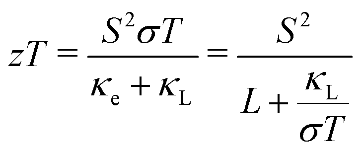
The rising demand for cooling, including refrigeration and air conditioning, poses environmental and economic challenges. Conventional cooling systems used in homes, vehicles, industries, and data centers are based on vapor-compression cycles utilizing coolants that are a major source of greenhouse gas emissions.1–4 The International Energy Agency reported that air conditioning is responsible for almost 20% of the electricity use in buildings globally,5 with some studies estimating up to 30–40% usage.6 Distributed thermoelectric (TE) cooling offers a viable solution,7 with studies demonstrating TE-based air conditioning8 and cooling powered by solar energy.9,10 In addition, low-temperature TE materials have applications in powering Internet of Things (IoT) devices,11 including low-power Arctic data sensors.12 Due to their diverse applications, there is a critical need for the discovery and development of low-temperature TE materials.Historically, narrow-gap semiconductors and semimetals have been found to exhibit good low-temperature TE performance. Bi2Te3, with a band gap of 0.14 eV, is the state-of-the-art TE material in the near-room temperature range (300–350 K).13 The recent demonstration of semimetallic Mg3Bi2-based materials with a peak zT of 0.9 at 350 K14 has renewed interest in low-temperature TE applications.15–17 Other narrow-gap semiconductors and semimetals such as CsBi4Te6,18 Bi1−xSbx,19 Cd3As2,20 ZrTe5,21 and correlated materials22 have also been studied for TE applications at or below room temperature. However, the coefficient of performance of current TE cooling devices (10–20% of the Carnot limit) is poor compared to vapor compression technology (50% of the Carnot limit under ideal conditions).7 Since the coefficient of performance increases with the TE figure of merit zT, it is important to search for new TE materials with high zT.
Computations have been instrumental in the discovery and development of new TE materials.23–28 Large-scale computationally-driven discovery of TE materials requires robust and tractable performance metrics or descriptors. Several such descriptors, including the electronic fitness function,29,30 Fermi surface complexity factor,31 and the quality factor32,33 have been proposed. In developing these material descriptors, it is typically assumed that the charge transport can be ascribed to a single carrier type (electrons or holes) and, therefore, the TE performance can be described within a single parabolic band approximation.34,35 While this is a reasonable approximation for materials with band gaps that are wide enough to avoid significant bipolar conduction, or even “gapped metals'' where a single charge carrier type dominates transport,36 it breaks down in materials where both electrons and holes are present in high concentrations, such as narrow-gap semiconductors and semimetals.37–39 Bipolar conduction increases the electrical conductivity while simultaneously decreasing the Seebeck coefficient and increasing the electronic thermal conductivity.40 As such, material descriptors for predicting the TE performance of narrow-gap semiconductors and semimetals must account for effects arising from bipolar conduction. One of the co-authors of this study has developed models to estimate the quality factor B – a material descriptor for predicting TE performance.32 Several high-throughput computational searches for new TE materials have been performed using B as a material descriptor.33,41–44 However, the models assume charge transport is dominated by either electrons or holes, not both. In this study, we derive new material descriptors for TE performance that account for bipolar conduction effects on charge transport properties.
Using semi-classical Boltzmann transport theory, we derive three important material descriptors for TE performance: (1) band gap, (2) n- and p-type TE quality factors, and (3) asymmetry parameter (ratio of the quality factors). We apply these material descriptors to search for new room-temperature TE materials among narrow-gap and semimetallic Zintl phases. In addition to the Zintl phases, we also calculate the material descriptors for Mg3Bi2, Bi2Te3, and Bi2Se3 as benchmark materials in this study. Consistent with experiments, we show that Mg3Bi2 and Bi2Te3 are high-performing TE materials near room temperature, which validates the predictive power of the descriptors. Through this search, we identify three Zintl phases (SrSb2, Zn3As2, and NaCdSb) with promising room-temperature TE performance. Lastly, we propose a refined TE quality factor, Bbp, which is a composite descriptor of the peak zT that can be used to compare the TE performances of narrow-gap semiconductors with significant bipolar conduction effects.
2. Theory: models and material descriptors
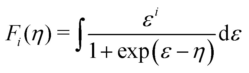
Carrier transport is often described in the Boltzmann transport theory framework.45–47 In the relaxation time approximation, the transport coefficients for isotropic bands is expressed in terms of the transport function Σ(E) as,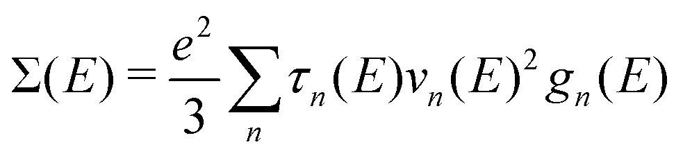 | (1) |
 | (2) |
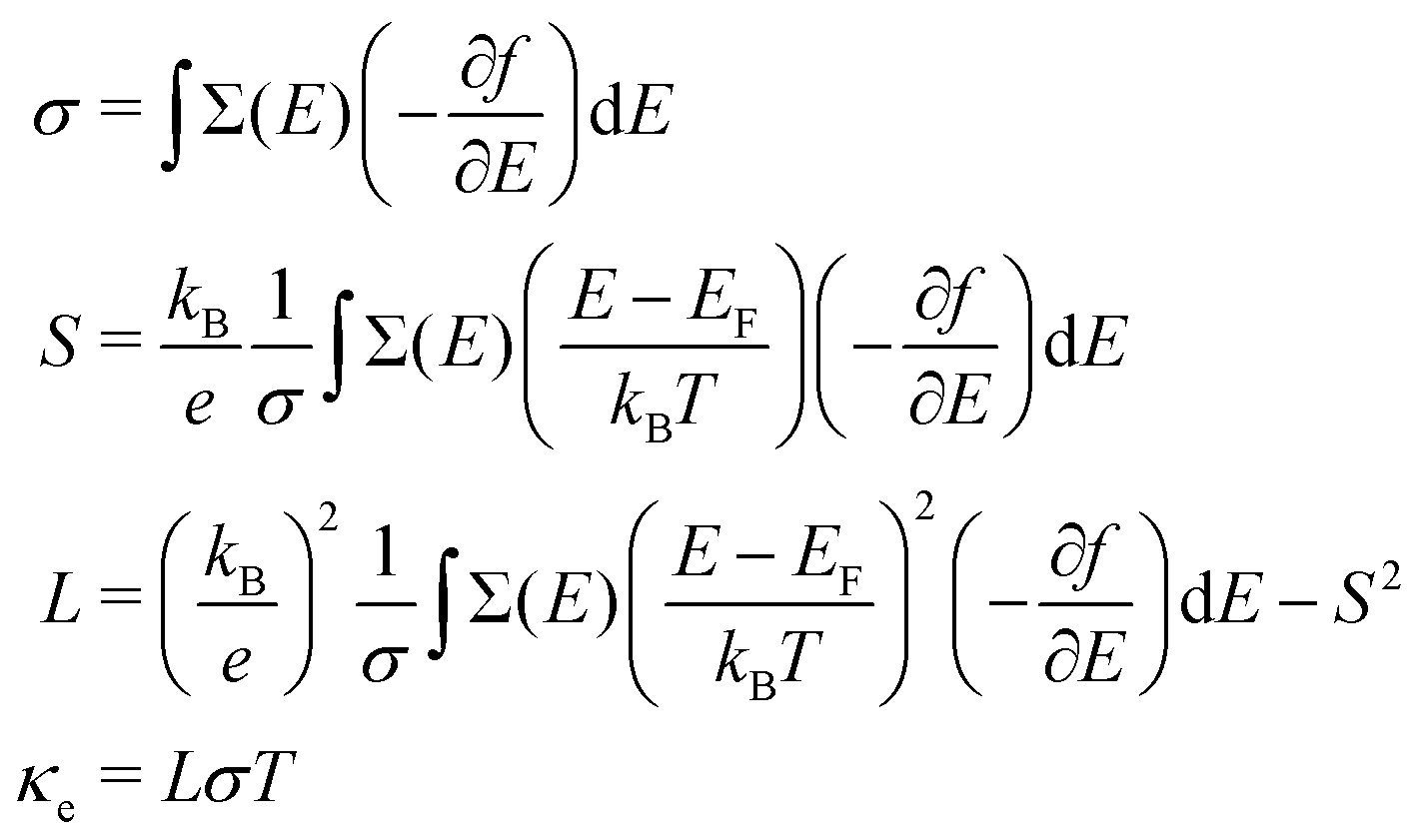 | (3) |
 | (4) |
 | (5) |
 | (6) |
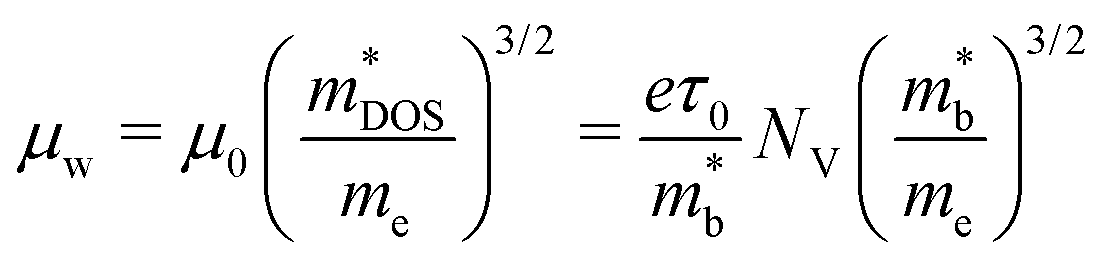
 is the density-of-states effective mass, which can be expressed in terms of band effective mass
  and valley degeneracy NV. The transport coefficients in eqn (4) must be revised when accounting for the effects of both electrons and holes (two-band model) on TE transport. The theory of the two-band model has been presented in detail elsewhere,37,54–57 but we briefly review it here to illustrate how the material descriptors are derived.
Here, we adopt the “majority” and “minority” carrier labels so that the theoretical expressions are applicable to both n-type (excess electrons) and p-type (excess holes) materials.58 We demonstrate that TE transport in narrow-gap semiconductors and semimetals depends on the asymmetry of the majority and minority carrier transport properties. We show this by considering isotropic conduction and valence bands with different effective masses and scattering times i.e., different weighted mobilities.
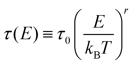
We can graphically understand the transport coefficients in a material with majority and minority carriers (Fig. 1). In isotropic and parabolic bands, squared group velocity varies linearly with energy E as v2(E) ∼ |E − Eb|, where Eb is the band edge. The density of states of a parabolic band is given by 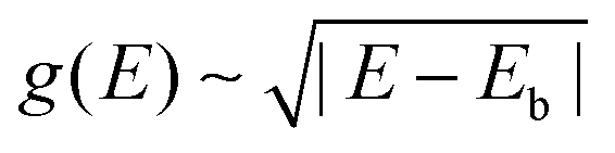 , and the scattering time due to polar optical phonons is expressed as
 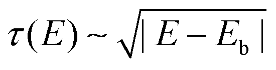 . By eqn (1), the transport distribution function follows a squared energy dependence Σ(E) ∼ (E − Eb)2 as shown in Fig. 1(d). The selection function −∂f/∂E, which peaks at the Fermi energy EF (Fig. 1e), samples Σ(E) in both the conduction and valence bands, resulting in contributions from both bands to the transport coefficients σ (Fig. 1f), S (Fig. 1g), and κe (Fig. 1h). The qualitative trends in the transport coefficients are not dependent on the scattering mechanism; similar results are obtained for acoustic deformation potential scattering (Fig. S1, ESI†).
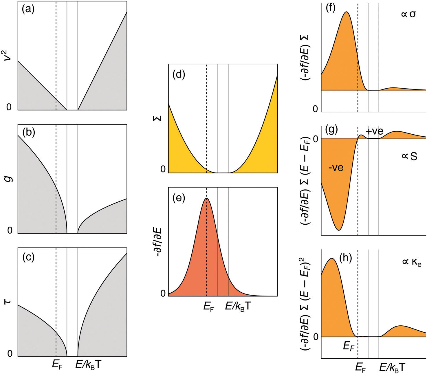 | ||
| Fig. 1 Transport coefficients in a two-band model. The valence and conduction band edges are shown as solid vertical lines, and the Fermi level EF is shown as a dotted vertical line. (a)–(c) The components of the transport function Σ(E) = v2(E)g(E)τ(E), shown in (d), where v(E), g(E), and τ(E) are the energy-dependent velocity, density of states, and scattering time, respectively. Σ(E) is sampled by the selection function −∂f/∂E, shown in (e), and weighted by (E − EF)m to obtain (f) the electrical conductivity σ (m = 0), (g) Seebeck coefficient S (m = 1), and (h) the Lorenz number (m = 2), which is related to the electronic thermal conductivity. The area under the curves are proportional to the magnitude of each transport coefficient at a fixed Fermi energy EF. | ||
Since the transport coefficients depend on the position of EF relative to the valence and conduction band edges, it is convenient to define a reduced Fermi energy for each band separately. If we reference EF to the majority carrier band edge i.e., EF = 0, then the reduced Fermi energy of majority carriers (ηmaj) and minority carriers (ηmin) are given by,
 | (7) |
In a two-band model, Σ(E) is the sum of the individual Σ(E) of the valence (VB) and conduction (CB) bands. As a result, the electrical conductivity σ in a two-band model is
| σ = σmaj + σmin | (8) |
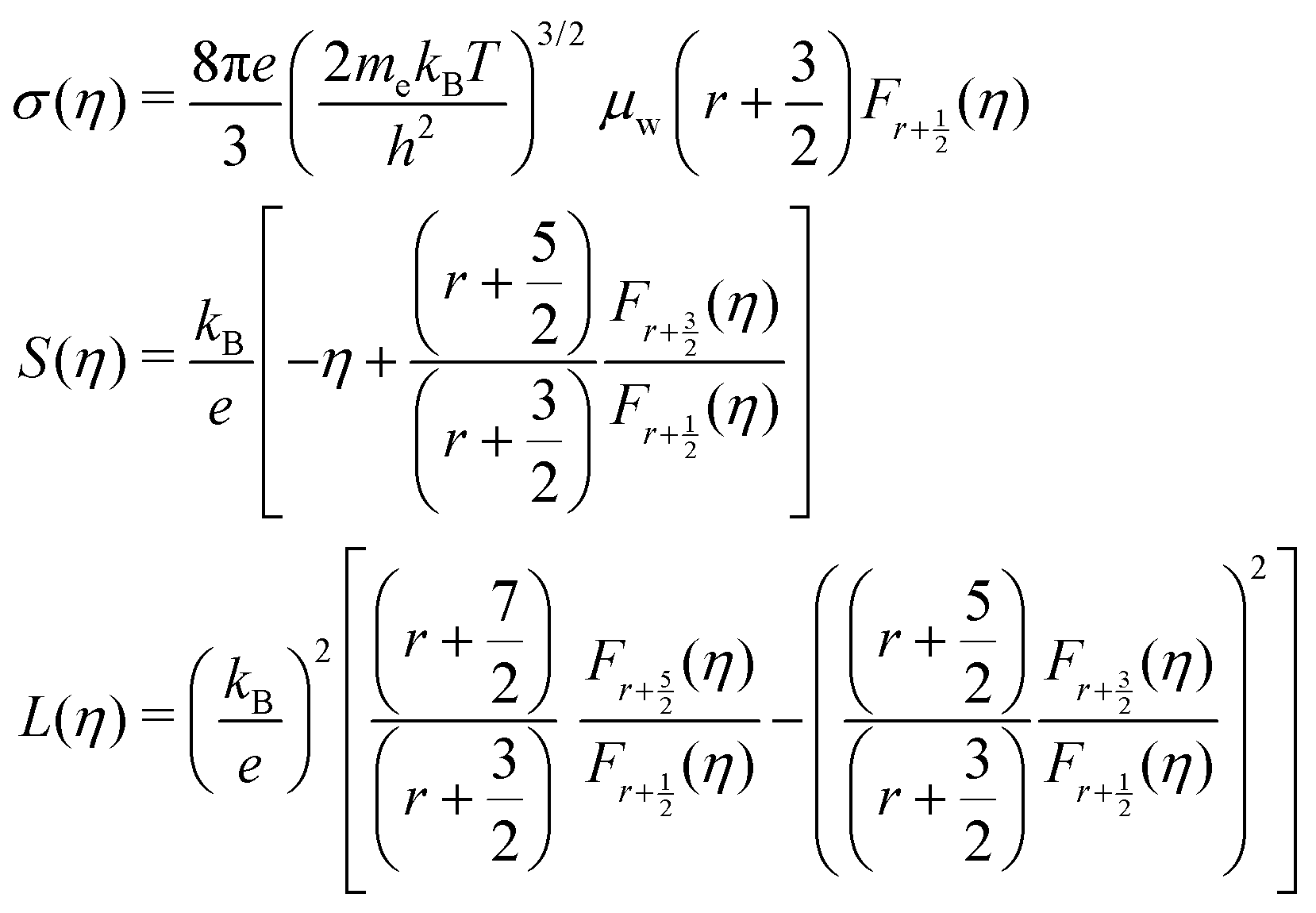
 | (9) |
 | (10) |
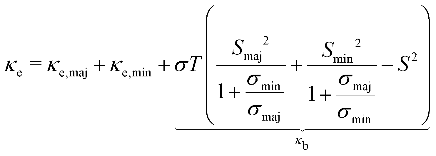 | (11) |
 | (12) |
 | (13) |
 | (14) |
Charge transport is regulated by the conductivity ratio σmaj/σmin, as it appears in S (eqn (9)) and κe (eqn (11)). From the single-band model (eqn (4)), the conductivity ratio is
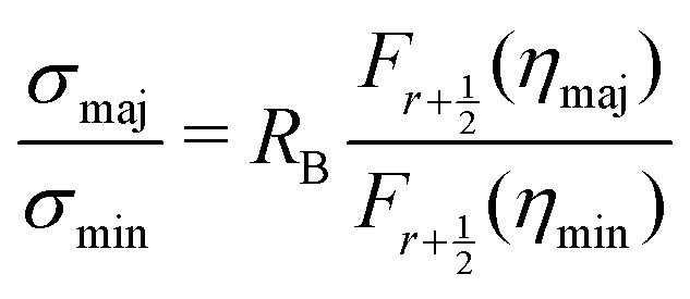 | (15) |
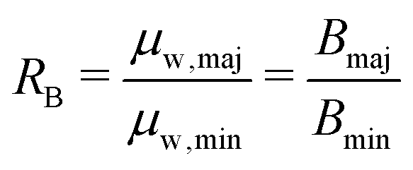 | (16) |
We compare zT for three representative cases of Eg: a semiconductor with a wide band gap (Fig. 2a), a narrow-gap semiconductor (Fig. 2b), and a semimetal (Fig. 2c). Regardless of Eg, higher Bmaj corresponds to higher zT for a given doping level η and temperature, as expected from a single-band model with no minority carriers.35,61 As the band gap decreases (0.5 eV → 0.05 eV → −0.05 eV), the maximum zT decreases due to the detrimental effects of bipolar conduction. This behavior can be understood from the individual transport coefficients in Fig. 3. σ is higher when the band gap is small or negative due to additive contributions from both electrons and holes (Fig. 3b). However, S decreases due to the partial cancellation of opposite charge carrier contributions (Fig. 3c), and the higher σ leads to a higher κe (Fig. 3d).
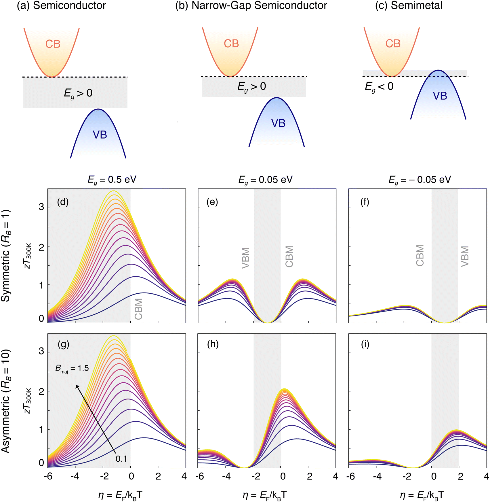 | ||
| Fig. 2 zT as a function of the reduced Fermi energy (η) at 300 K for (a) semiconductors, (b) narrow-gap semiconductors, and (c) semimetals. The zT vs. η curves are plotted at 300 K for different Bmaj, as defined in eqn (14), assuming majority carriers are electrons. Bmaj values range from 0.1 (dark blue) to 1.5 (yellow) in 0.1 increments. Panels (d)–(f) for the symmetric (RB = 1) case, and panels (g)–(i) illustrate the case of large asymmetry (RB = 10). For materials with narrow or negative band gap, large RB is favorable for TE performance due to minimization of bipolar conduction effects. | ||
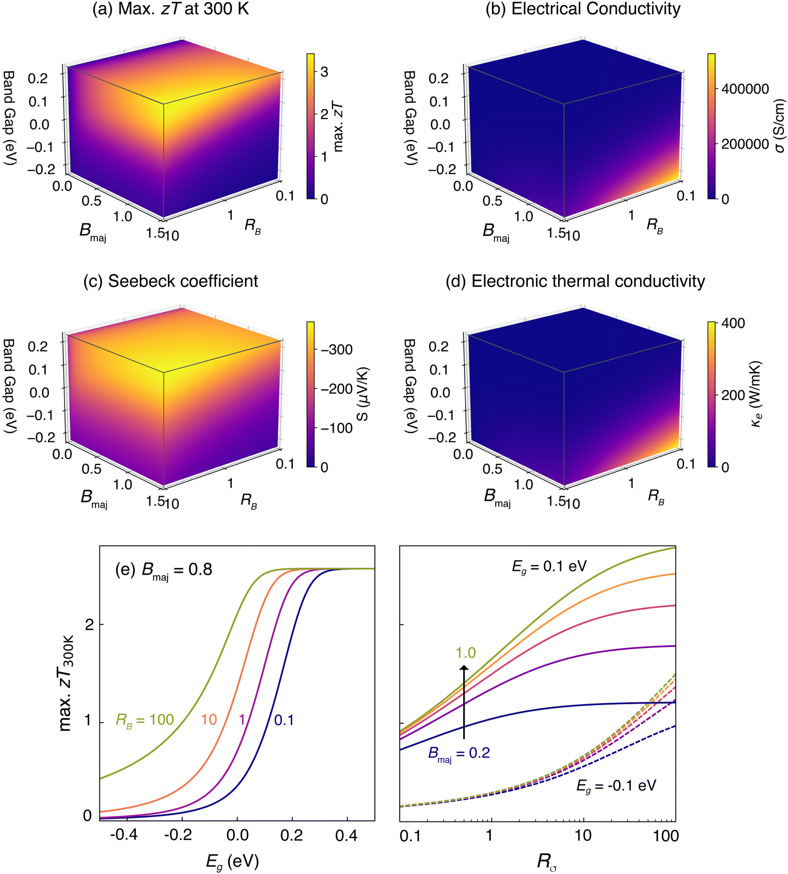 | ||
| Fig. 3 (a) Maximum zT at 300 K as a function of band gap (Eg), majority carrier quality factor (Bmaj), and asymmetry parameter (RB). The electrical conductivity (b), Seebeck coefficient (c), and electronic thermal conductivity (d) are shown at the EF where zT is maximized at 300 K. (e) Maximum zT at 300 K as a function of band gap, assuming Bmaj = 0.8. Each curve corresponds to different RB. (f) Maximum zT at 300 K for different RB, shown for Eg = 0.1 eV (solid) and Eg = −0.1 eV (dashed). Each curve corresponds to different Bmaj. Wide-gap materials exhibit high zT; however, high TE performance is also achieved in narrow-gap semiconductors and semimetals with high Bmaj and RB. | ||
Bipolar conduction effects in narrow-gap semiconductors and semimetals can be partially minimized when Bmin is lower than Bmaji.e., RB > 1. We show this by contrasting zT when the quality factors are nearly the same (Fig. 2d–f) vs. asymmetric (Fig. 2g–i). zT is nearly unaffected by RB when the band gap is sufficiently large (Fig. 2d and g). However, the benefit of a higher RB is more noticeable when the band gap is smaller; in particular, zT is higher for a given doping level and temperature when RB is higher (Fig. 2e, f, h, i). For a given Bmaj, a higher RB = Bmaj/Bmin corresponds to a lower Bmin, meaning that we minimize minority carrier contributions to the overall TE transport. σ of minority carriers therefore decreases for higher RB, leading to a decrease in the overall σ (Fig. 3b). However, κe is correspondingly lower (Fig. 3d) and, more notably, the magnitude of the Seebeck coefficient is higher because the cancellation of opposite charge carriers is minimized (Fig. 3c). In effect, higher asymmetry between the quality factor of majority and minority carriers mitigates the detrimental effects of bipolar conduction in narrow-gap semiconductors and semimetals. We arrive at the same qualitative conclusions regardless of the scattering mechanism, as evident from comparing Fig. 2, 3 and Fig. S2, S3 (ESI†).
It is worth noting cases where transport by majority and minority carriers are asymmetric but in favor of minority carriers, i.e., RB < 1. For a given Eg, zT is lower when RB < 1 as illustrated in Fig. 3e and f. Since the transport properties of minority carriers in this case are favorable over those of majority carriers, zT is maximized only when the material is nearly intrinsic and the concentrations of opposite carrier types are roughly the same (Fig. S4, ESI†). The implication of RB < 1 is that the material will display better TE performance by switching the majority carrier type. For example, if RB < 1 and electrons are assumed to be the majority carriers, the material will be better as a p-type material instead when holes are the majority carrier type. This is consistent with the overall framework. In summary,
1. Semiconductors with large Eg will not suffer from bipolar conduction effects and exhibit higher maximum zT.
2. Large Bmaj indicates high TE performance in the absence of bipolar conduction.
3. zT of narrow-gap semiconductors and semimetals is sensitive to the asymmetry parameter i.e., RB = Bmaj/Bmin. When the asymmetry is in favor of the majority carriers i.e., RB > 1, the material exhibits higher zT because bipolar conduction effects are minimized.
Therefore, we use Eg, Bmaj, and RB as material descriptors to search for room-temperature TE materials that are narrow-gap semiconductors or semimetals. Prior studies have identified the importance of transport asymmetry to minimize bipolar conduction and achieve high power factors in narrow gap materials.62–64 Our analysis is in agreement with these prior studies. However, these studies relied on either full-zone electrical transport calculations or a large number of descriptors obtained through parameter combinations. In contrast, we derive the functional dependence of TE performance on RB from the two-band model. Also, prior work has focused on narrow-gap materials. Our proposed descriptors are applicable to both narrow-gap semiconductors and semimetals, which is important to account for well-known low-temperature TE materials such as Mg3Bi2.
3. Application: search for narrow-gap and semimetallic thermoelectric materials
3.1 Computational workflow
We apply the proposed material descriptors to computationally search for room-temperature TE materials among narrow-gap and semimetallic Zintl phases. The search focuses on Zintl phases because they are known to have narrow and negative band gaps, and generally exhibit good TE performance.65 The tiered computational workflow is depicted in Fig. 4. Details of the density functional theory (DFT) and other calculations, as well as the workflow, are provided in Section 6.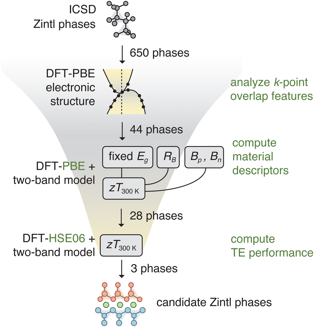 | ||
| Fig. 4 Computational workflow to identify Zintl phases that are narrow-gap semiconductors or semimetals and exhibit high room-temperature thermoelectric performance. Eg is the band gap, RB is the asymmetry parameter, and Bmaj and Bmin are the quality factors of majority and minority carriers. PBE and HSE06 refer to DFT functionals (see Methods). | ||
Out of 650 Zintl phases from the Inorganic Crystal Structure Database (ICSD), we identify 44 phases that are potentially narrow-gap semiconductors or semimetals using DFT with the semilocal PBE functional. By calculating the maximum zT at 300 K (Section 2), we identify 28 promising Zintl phases, for which we perform more accurate electronic structure calculations with a hybrid DFT functional. The computed material descriptors for these 28 phases, in addition to the benchmark materials Mg3Bi2, Bi2Te3, and Bi2Se3, are reported in Table S1 (ESI†). The predicted zTmax at 300 K as a function of the transport asymmetry (RB) and band gap (Eg) are plotted in Fig. 5a. Below, we discuss the material descriptors and predicted TE performance of Mg3Bi2, Bi2Te3, and the three best candidate Zintl phases.
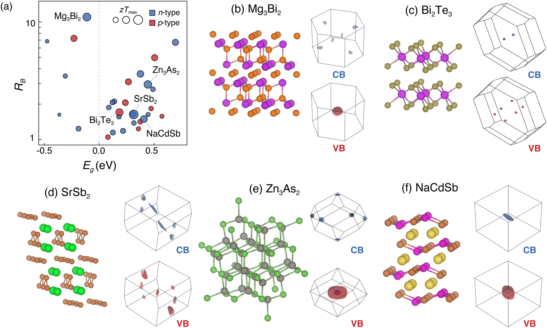 | ||
| Fig. 5 (a) Predicted thermoelectric performance of 31 phases plotted as a function of the transport asymmetry (RB) and the band gap (Eg). The marker size scales with the maximum zT at 300 K using the two-band model. The maximum zT are reported in Table 1. The crystal structures and Fermi surfaces of the conduction band (blue, labeled “CB”) and valence band (red, labeled “VB”) are shown for (b) Mg3Bi2, (c) Bi2Te3, and three candidate materials: (d) SrSb2, (e) Zn3As2, (f) and NaCdSb. | ||
3.2 Validation and materials recommendations
![[thin space (1/6-em)]](https://www.rsc.org/images/entities/char_2009.gif) K) among the narrow-gap and semimetallic Zintl phases considered in this study (Fig. 5a). In fact, the predicted zTmax of 0.32 at 300 K (Table 1) is close to the experimental value when doped with Te (zT ∼ 0.3). The “rediscovery” of Mg3Bi2 provides validation for our computational search workflow. Note that high TE performance at room temperature is achieved by alloying Mg3Bi2 with Mg3Sb2.14 Mg3Sb2 also has a large conduction band degeneracy of 6,67 which yields a large RB of 7.6, and zT300K = 0.28 for n-type (Table S1, ESI†).
K) among the narrow-gap and semimetallic Zintl phases considered in this study (Fig. 5a). In fact, the predicted zTmax of 0.32 at 300 K (Table 1) is close to the experimental value when doped with Te (zT ∼ 0.3). The “rediscovery” of Mg3Bi2 provides validation for our computational search workflow. Note that high TE performance at room temperature is achieved by alloying Mg3Bi2 with Mg3Sb2.14 Mg3Sb2 also has a large conduction band degeneracy of 6,67 which yields a large RB of 7.6, and zT300K = 0.28 for n-type (Table S1, ESI†).
| Compound | E g | N V,VB | B p | N V,CB | B n | R B | max. zT300K |
n-/p-type |
|---|---|---|---|---|---|---|---|---|
| Mg3Bi2 | −0.11 | 1 | 0.002 | 6 | 0.021 | 11.0 | 0.32 | n |
| Bi2Te3 | 0.18 | 6 | 0.011 | 2 | 0.006 | 1.7 | 0.26 | p |
| Bi2Se3 | 0.32 | 1 | 0.003 | 1 | 0.004 | 1.4 | 0.11 | n |
| SrSb2 | 0.32 | 3 | 0.011 | 4 | 0.018 | 1.6 | 0.39 | n |
| Zn3As2 | 0.44 | 2 | 0.004 | 3 | 0.012 | 2.9 | 0.29 | n |
| NaCdSb | 0.41 | 2 | 0.006 | 2 | 0.009 | 1.5 | 0.23 | n |
K of 0.39, which is 1.22× larger compared to Mg3Bi2 and 1.5× compared to Bi2Te3. SrSb2 has been used as a precursor for synthesizing Sr-filled CoSb3 through arc-melting,70,71 and small grains of SrSb2 have been observed in the samples.70 However, detailed characterization of transport properties has so far not been reported. Our predictions make SrSb2 an interesting candidate to pursue experimentally.
![[3 with combining macron]](https://www.rsc.org/images/entities/char_0033_0304.gif) , no. 206) and is one of several polymorphs of Zn3As2.72 Several other polymorphs of Zn3As2 are known, including the room-temperature α phase (I41/acd),73 the high-temperature α′ phase (P42/nbc),74,75 another high-temperature β phase (Fmm),76 and the high-temperature, high-pressure α′′ phase (P42/nmc).77,78 The TE properties of Cd3As2–Zn3As2 alloys have been studied,79–82 but the transport properties of the Ia phase has not been measured. There are three conduction bands that are close in energy and located at the Brillouin zone edges (Fig. 5e), yielding a valley degeneracy NV,CB of 3. There are two valence bands close in energy at the Γ-point, yielding a valley degeneracy NV,VB of 2. Despite a modest RB of 2.9, the relatively large band gap of 0.44 eV facilitates a high TE performance. The lower performance compared to SrSb2 is primarily due to the smaller Bn.
K of NaCdSb to be 72% of the maximum zT300K of Mg3Bi2. Guo et al. recently reported experimentally measured zT300K of 0.2 without optimizing the carrier concentration.85 The highest zT of the material was found to be 1.3 at 673 K.
, no. 206) and is one of several polymorphs of Zn3As2.72 Several other polymorphs of Zn3As2 are known, including the room-temperature α phase (I41/acd),73 the high-temperature α′ phase (P42/nbc),74,75 another high-temperature β phase (Fmm),76 and the high-temperature, high-pressure α′′ phase (P42/nmc).77,78 The TE properties of Cd3As2–Zn3As2 alloys have been studied,79–82 but the transport properties of the Ia phase has not been measured. There are three conduction bands that are close in energy and located at the Brillouin zone edges (Fig. 5e), yielding a valley degeneracy NV,CB of 3. There are two valence bands close in energy at the Γ-point, yielding a valley degeneracy NV,VB of 2. Despite a modest RB of 2.9, the relatively large band gap of 0.44 eV facilitates a high TE performance. The lower performance compared to SrSb2 is primarily due to the smaller Bn.
K of NaCdSb to be 72% of the maximum zT300K of Mg3Bi2. Guo et al. recently reported experimentally measured zT300K of 0.2 without optimizing the carrier concentration.85 The highest zT of the material was found to be 1.3 at 673 K.
4. Thermoelectric quality factor for narrow-gap semiconductors
We identified three material descriptors that are important to describe the TE performances of narrow-gap semiconductors and semimetals: majority carrier quality factor (Bmaj), band gap (Eg), and the asymmetry parameter (RB). We used these descriptors to efficiently search for new TE materials with narrow or negative band gaps for room-temperature TE applications. Our search methodology based on these descriptors is distinct from previous studies that assume absence of minority carrier effects.29,32 In the case of single-band transport, the maximum zT of a material is solely determined by the quality factor (B) of the majority carriers and it monotonically increases with B (Fig. S5, ESI†). Prior studies have used B as a descriptor to search for high-performing TE materials.32,86,87 However, a composite descriptor that provides a measure of peak zT i.e., optimized with respect to doping and temperature, for two-band transport is currently missing. To address this need, we propose a refined TE quality factor, Bbp, where “bp” denotes “bipolar”.B bp is a useful descriptor of TE performance when both majority and minority carriers significantly contribute to charge transport, for example, in narrow-gap semiconductors. The mathematical form of Bbp should ideally have the following characteristics: (i) increase monotonically with peak zT, (ii) include Bmaj, Eg, and RB, and (iii) be interpretable to understand the relative contribution of each parameter to peak zT. Liu et al. defined a parameter B*, which describes the relative contributions of two of the three descriptors, Bmaj and Eg, towards the peak zT:88–90
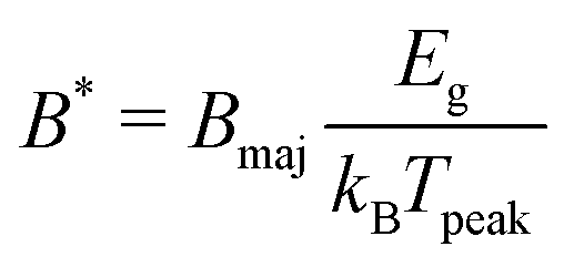 | (17) |
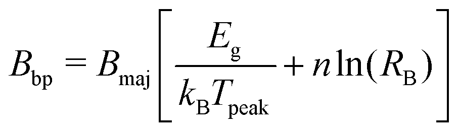 | (18) |
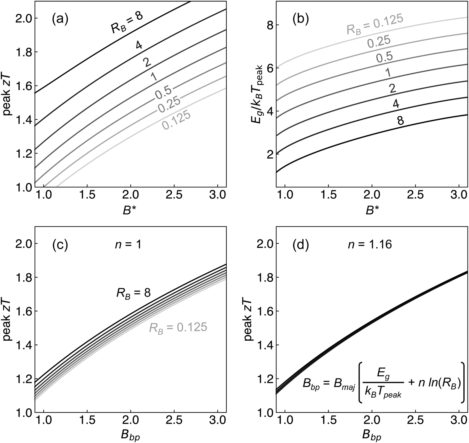 | ||
| Fig. 6 (a) Peak zT and (b) Eg/kBTpeak plotted against B* (eqn (17)) for different values of RB. Peak zT plotted against Bbp (eqn (18)) is shown for (c) n = 1 and (d) n = 1.16. | ||
We calculate Bbp and the corresponding peak zT for the narrow-gap Zintl phases (Fig. S7, ESI†). We find that candidate materials identified in our search (SrSb2, Zn3As2, and NaCdSb) have fairly high Bbp values, as well as other Zintl phases such as Mg2ZnAs2, NaZn4As3, and Li4Ba3As4. We note that ranking the TE performances of narrow-gap semiconductors with Bbp is fundamentally different from the search methodology employed in Section 3. Bbp is a measure of the peak performance at the corresponding Tpeak and optimized doping level. Tpeak need not be 300 K, which was the focus of the search presented in Section 3. On the other hand, using Bmaj, Eg, and RB as separate descriptors allows us to compare the TE performances of materials at assumed temperatures or doping levels, or both. In Section 3 for example, we rank the TE performance of Zintl phases at room temperature (300 K). Using the individual descriptors (Bmaj, Eg, RB) allow us to search for materials for specific low-temperature applications, for example, at or near room temperature for IoT sensors.11,12
5. Conclusions
We use an analytical two-band model to derive material descriptors for predicting the TE performances of narrow-gap semiconductors and semimetals. The proposed descriptors are obtained from simple DFT calculations, which allows reliable, high-throughput search of narrow-gap semiconductors and semimetals for low-temperature thermoelectrics. We find that the material descriptors that govern TE performance are: (1) the majority carrier quality factor (Bmaj), (2) the band gap (Eg), and (3) the asymmetry in the transport properties of majority and minority carriers (RB = Bmaj/Bmin), where Bmin is the minority carrier quality factor. As in a single-band model, materials with high quality factors tend to exhibit high TE performance when doping is optimized. However, high TE performance in narrow-gap semiconductors and semimetals also hinges on minimizing bipolar conduction effects, which is achieved when majority and minority carrier transport is asymmetric, i.e., when RB is large. Using the proposed material descriptors, we assess the TE performances of a set of narrow-gap and semimetallic Zintl phases. In agreement with experiments, we correctly re-identify Mg3Bi2 and Bi2Te3 as high-performing TE materials for room-temperature applications. In particular, Mg3Bi2 showcases the importance of transport asymmetry; despite being a semimetal, a large RB ensures high room-temperature TE performance. From our search, we find three Zintl phases (SrSb2, Zn3As2, and NaCdSb) that exhibit high room-temperature TE performance. We further propose a refined TE quality factor, Bbp, which is a useful measure of the TE performance when bipolar conduction effects are significant. Bbp combines the individual descriptors (Bmaj, Eg, and RB) into a single metric to assess the peak zT of materials.While the descriptors help to identify candidate TE materials, there are others factors that require careful consideration for practical applications. The temperature-dependence of Eg for example may affect the predicted maximum zT at 300 K. The negative Eg of Mg3Bi2 changes by ∼25 meV within a range of 350 K,14 and Eg of Bi2Te3 changes by ∼100 meV within a range of 600 K.91 We find that for Bi2Te3 and the three candidate Zintl phases, maximum zT at 300 K does not change significantly if the band gap is changed by 25 meV or 100 meV (Table S2, ESI†). Maximum zT of Mg3Bi2 however, owing to its negative band gap, is most sensitive to changes in Eg, as illustrated in Fig. 3e. Oxidation is another consideration for terrestrial applications.92 Near room-temperature operation will reduce the effects of oxidation due to sluggish kinetics, but experimental verification is needed especially for materials containing alkali and alkaline-earth elements. Materials also need to be doped to optimize TE performance. Generally, narrow band gap semiconductors are more easily dopable compared to wide-gap insulators due to low concentrations of charge compensating native defects.93 Future work should address these key considerations in optimizing the TE performance of the candidate materials.
6. Computational methodology
A schematic of the computational workflow is shown in Fig. 4. We use first-principles density functional theory (DFT) to perform structural relaxations, and to calculate electronic band structures and bulk moduli. All DFT calculations are performed with the Vienna ab initio simulation package (VASP)94,95 and the projector augmented wave (PAW) method is used to describe the core electrons.96,97 The wavefunctions are expanded as plane waves with an energy cutoff of 340 eV.First, we relax the ICSD structures of 650 Zintl phases using the generalized gradient approximation (GGA) of Perdew–Burke–Ernzerhof (PBE)98 as the exchange correlation functional and an automatically-generated Γ-centered k-point mesh with length factor Rk = 20. We apply on-site Hubbard U corrections on the d orbitals of certain transition metals, following the methodology in ref. 41 and 99. For the relaxed structures, we computed their electronic structures on a dense Γ-centered k-mesh determined by the equation Natoms × Nkpts ≈ 8000, where Natoms and Nkpts are the number of atoms in the primitive cell and number of k-points, respectively.43,44 This translates to a k-point grid of 14 × 14 × 8 for Mg3Bi2 and 12 × 12 × 12 for Bi2Te3. We include relativistic spin–orbit coupling (SOC) effects in these calculations.
Next, we analyze features of the electronic structures calculated with the PBE functional. It is well-known that semilocal DFT functionals such as GGA-PBE tend to severely underestimate the band gaps of materials, while predictions with hybrid functionals (e.g., HSE06) are generally more reliable for semiconductors and insulators.100–102 However, the large computational cost associated with hybrid functionals makes them unsuitable for high-throughput calculations. Within the dataset of 650 Zintl phases, we focus on compounds that have zero or negative band gap in GGA-PBE calculations and try to identify potentially narrow-gap semiconductors and semimetals. We choose to focus on this subset of materials to demonstrate the usefulness of the descriptors in materials where bipolar conduction cannot be ignored. The specific procedure we have adopted to identify narrow-gap semiconductors and semimetals is not important because the descriptors are generally applicable irrespective of the band gap.
We analyze the band occupations to assess the extent of band overlap (nesting) near the Fermi level. In a typical semiconductor with a well-defined band gap, bands below the Fermi level are fully occupied (valence bands) and those above are unoccupied (conduction bands) at 0 K (DFT calculation). In this case, there are no partially occupied bands. In contrast, a metal is characterized by overlapping bands with partial occupancies at numerous k-points around the Fermi level. We therefore evaluate the fraction of partially-occupied k-points relative to the total number of sampled k-points. If this fraction is small, it is possible that the material is a narrow-gap semiconductor or semimetal, but less likely to be a true metal. Specifically, we calculate the ratio,
 | (19) |
We use N = 3 and occupation tolerance δ = 10−3 to calculate R. R varies between 0 and 1, with R = 0 representing a semiconductor and large R indicating that the phase is likely a metal (Fig. S8, ESI†). We classified materials with 0 < R ≤ 0.1 from the GGA-PBE electronic structure as potential narrow-gap semiconductors and semimetals because of the small overlap between the nominal valence and conduction bands. Among the 650 Zintl phases, we identify 44 that have R ≤ 0.1.
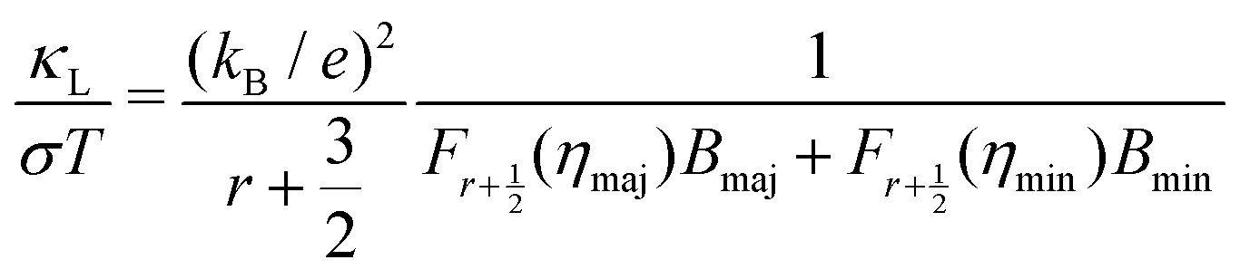
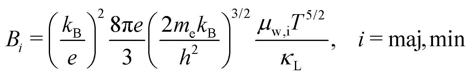
For these 44 Zintl phases, we then estimate the maximum zT at 300 K using the two-band transport model (eqn (12)). Three independent material descriptors are necessary to estimate zT: band gap (Eg), n- and p-type quality factors (Bn and Bp), and asymmetry parameter (RB). Due to the unsystematic underestimation of the band gap in GGA-PBE calculations, we fix Eg to 0.3 eV for all 44 phases. Since larger Eg leads to higher zT (Fig. 3), fixing Eg to 0.3 eV allows us to compare the best-case-scenario zT across materials. We perform a scissor operation to adjust Eg with the assumption that the band geometry remains unchanged. The band effective mass  is an important parameter in calculating the quality factors and, therefore, RB. We use a finite-difference method to calculate
  from the electronic structure calculated on a dense k-point grid.103 We also calculate the density-of-states effective mass
  from
from  using the relation
 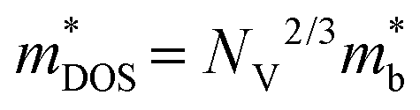 , where NV is the valley degeneracy. The quality factors are then calculated using eqn (14), where μ0 and κL at 300 K are calculated using semi-empirical models that are fitted to large experimental datasets (see ref. 32 and 86 for details). The bulk modulus, which is an input parameter for the semi-empirical models, is calculated by fitting the Birch–Murnaghan equation of state to a set of total energies at different volumes.104 In each case, we adjust the Fermi energy to maximize zT at 300 K.
Due to the recent success of Mg3Bi2-based materials for low- and room-temperature TE applications,14 we compare the estimated maximum zT of the 44 Zintl phases to that of Mg3Bi2. We find that 20 out of the 44 Zintl phases have an estimated maximum zT of more than 20% of the maximum zT of Mg3Bi2 at 300 K. We perform higher accuracy electronic structure calculations with the hybrid HSE06 functional on the 20 phases, in addition to 8 randomly-chosen Zintl phases out of the remaining 24 phases. The exchange mixing parameter is set to 25%, and all HSE06 calculations include spin–orbit coupling effects. The structures are relaxed with HSE06 prior to calculating the electronic structure. We use the HSE06 electronic structure to calculate Eg and  , which are then used as inputs to estimate the maximum zT at 300 K. The corresponding results are shown in Fig. 5a and tabulated in Table 1 and Table S1 (ESI†).
Author contributions
Michael Y. Toriyama: conceptualization, investigation, data curation, writing (original draft), writing (editing). Adam N. Carranco: investigation, data curation, writing (editing). G. Jeffrey Snyder: investigation, writing (editing), supervision. Prashun Gorai: conceptualization, investigation, data curation, writing (editing), supervision, project administration.Conflicts of interest
There are no conflicts to declare.Acknowledgements
M. Y. T. is funded by the United States Department of Energy through the Computational Science Graduate Fellowship (DOE CSGF) under grant number DE-SC0020347. A. N. C. was funded by the Mines Undergraduate Research Fellowship (Colorado School of Mines). G. J. S. acknowledges award 70NANB19H005 from U.S. Department of Commerce, National Institute of Standards and Technology as part of the Center for Hierarchical Materials Design (CHiMaD). P.G. acknowledges support from NSF through award DMR-2102409. The research was performed using computational resources sponsored by the Department of Energy's Office of Energy Efficiency and Renewable Energy and located at the NREL.References
- Y. Dong, M. Coleman and S. A. Miller, Annu. Rev. Env. Resour., 2021, 46, 59 CrossRef.
- J. M. Calm, Int. J. Refrig., 2006, 29, 833 CrossRef CAS.
- B. Xiang, P. K. Patra, S. A. Montzka, S. M. Miller, J. W. Elkins, F. L. Moore, E. L. Atlas, B. R. Miller, R. F. Weiss, R. G. Prinn and S. C. Wofsy, Proc. Natl. Acad. Sci. U. S. A., 2014, 111, 17379 CrossRef CAS PubMed.
- P. Purohit and L. Höglund-Isaksson, Atmos. Chem. Phys., 2017, 17, 2795 CrossRef CAS.
- The Future of Cooling, https://www.iea.org/reports/the-future-of-cooling.
- X. Zhou, D. Yan, J. An, T. Hong, X. Shi and X. Jin, Energ. Buildings, 2018, 169, 344 CrossRef.
- G. J. Snyder, S. LeBlanc, D. Crane, H. Pangborn, C. E. Forest, A. Rattner, L. Borgsmiller and S. Priya, Joule, 2021, 5, 748 CrossRef CAS.
- Q. Liu, F. Wei, G. Li, Z. Kan, J. Yang, H. Zhu, B. Wang and H. Zhao, iScience, 2022, 25, 104296 CrossRef CAS PubMed.
- M. Abdullah, J. Ngui, K. Abd Hamid, S. Leo and S. Tie, Energ. Fuel, 2009, 23, 5677 CrossRef CAS.
- H. Moria, M. Ahmed, A. Alghanmi, T. I. Mohamad and Y. Yaakob, Energy Procedia, 2019, 158, 198 CrossRef.
- D. Narducci, J. Phys. Energy, 2019, 1, 024001 CrossRef CAS.
- A. Grigoriev, S. Grigoriev, A. Korolev, O. Losev, D. Mel’nik, V. Skorlygin and A. Frolov, Atom. Energy, 2019, 125, 231 CrossRef CAS.
- I. T. Witting, T. C. Chasapis, F. Ricci, M. Peters, N. A. Heinz, G. Hautier and G. J. Snyder, Adv. Electron. Mater., 2019, 5, 1800904 CrossRef.
- J. Mao, H. Zhu, Z. Ding, Z. Liu, G. A. Gamage, G. Chen and Z. Ren, Science, 2019, 365, 495 CrossRef CAS PubMed.
- Y. Liu, L. Yin, W. Zhang, J. Wang, S. Hou, Z. Wu, Z. Zhang, C. Chen, X. Li, H. Ji, Q. Zhang, Z. Liu and F. Cao, Cell Rep. Phys. Sci., 2021, 2, 100412 CrossRef CAS.
- Z. Liu, W. Gao, H. Oshima, K. Nagase, C.-H. Lee and T. Mori, Nat. Commun., 2022, 13, 1120 CrossRef CAS PubMed.
- J. Yang, G. Li, H. Zhu, N. Chen, T. Lu, J. Gao, L. Guo, J. Xiang, P. Sun, Y. Yao, R. Yang and H. Zhao, Joule, 2022, 6, 193 CrossRef CAS.
- D.-Y. Chung, T. P. Hogan, M. Rocci-Lane, P. Brazis, J. R. Ireland, C. R. Kannewurf, M. Bastea, C. Uher and M. G. Kanatzidis, J. Am. Chem. Soc., 2004, 126, 6414 CrossRef CAS PubMed.
- R. Wolfe and G. Smith, Appl. Phys. Lett., 1962, 1, 5 CrossRef CAS.
- H. Wang, X. Luo, W. Chen, N. Wang, B. Lei, F. Meng, C. Shang, L. Ma, T. Wu, X. Dai, Z. Wang and X. Chen, Sci. Bull., 2018, 63, 411 CrossRef CAS PubMed.
- S. A. Miller, I. Witting, U. Aydemir, L. Peng, A. J. Rettie, P. Gorai, D. Y. Chung, M. G. Kanatzidis, M. Grayson, V. Stevanović, E. S. Toberer and G. J. Snyder, Phys. Rev. Appl., 2018, 9, 014025 CrossRef CAS.
- J. M. Tomczak, J. Phys.: Condens. Matter, 2018, 30, 183001 CrossRef PubMed.
- P. Gorai, V. Stevanović and E. S. Toberer, Nat. Rev. Mater., 2017, 2, 1 Search PubMed.
- G. K. Madsen and D. J. Singh, Comput. Phys. Commun., 2006, 175, 67 CrossRef CAS.
- G. K. Madsen, J. Carrete and M. J. Verstraete, Comput. Phys. Commun., 2018, 231, 140 CrossRef CAS.
- A. Faghaninia, J. W. Ager III and C. S. Lo, Phys. Rev. B: Condens. Matter Mater. Phys., 2015, 91, 235123 CrossRef.
- J.-J. Zhou, J. Park, I.-T. Lu, I. Maliyov, X. Tong and M. Bernardi, Comput. Phys. Commun., 2021, 264, 107970 CrossRef CAS.
- T. Deng, G. Wu, M. B. Sullivan, Z. M. Wong, K. Hippalgaonkar, J.-S. Wang and S.-W. Yang, npj Comput. Mater., 2020, 6, 1 CrossRef.
- G. Xing, J. Sun, Y. Li, X. Fan, W. Zheng and D. J. Singh, Phys. Rev. Mater., 2017, 1, 065405 CrossRef.
- R. Li, X. Li, L. Xi, J. Yang, D. J. Singh and W. Zhang, ACS Appl. Mater. Inter., 2019, 11, 24859 CrossRef CAS PubMed.
- Z. M. Gibbs, F. Ricci, G. Li, H. Zhu, K. Persson, G. Ceder, G. Hautier, A. Jain and G. J. Snyder, npj Comput. Mater., 2017, 3, 1 CrossRef CAS.
- J. Yan, P. Gorai, B. Ortiz, S. Miller, S. A. Barnett, T. Mason, V. Stevanović and E. S. Toberer, Energ. Environ. Sci., 2015, 8, 983 RSC.
- P. Gorai, P. Parilla, E. S. Toberer and V. Stevanovic, Chem. Mater., 2015, 27, 6213 CrossRef CAS.
- A. F. May and G. J. Snyder, Materials, preparation, and characterization in thermoelectrics, CRC press, 2017, p. 207 Search PubMed.
- S. D. Kang and G. J. Snyder, arXiv preprint arXiv:1710.06896, 2017.
- F. Ricci, A. Dunn, A. Jain, G.-M. Rignanese and G. Hautier, J. Mater. Chem. A, 2020, 8, 17579 RSC.
- T. Chasapis, D. Koumoulis, B. Leung, N. Calta, S.-H. Lo, V. Dravid, L.-S. Bouchard and M. Kanatzidis, APL Mater., 2015, 3, 083601 CrossRef.
- H. Naithani, E. Müller and J. De Boor, J. Phys. Energy, 2022, 4, 045002 CrossRef.
- H. Wang, R. Gurunathan, C. Fu, R. Cui, T. Zhu and G. J. Snyder, Mater. Adv., 2022, 3, 734 RSC.
- L. Zhang, P. Xiao, L. Shi, G. Henkelman, J. B. Goodenough and J. Zhou, J. Appl. Phys., 2015, 117, 155103 CrossRef.
- P. Gorai, E. S. Toberer and V. Stevanović, Phys. Chem. Chem. Phys., 2016, 18, 31777 RSC.
- S. A. Miller, P. Gorai, U. Aydemir, T. O. Mason, V. Stevanović, E. S. Toberer and G. J. Snyder, J. Mater. Chem. C, 2017, 5, 8854 RSC.
- P. Gorai, A. Ganose, A. Faghaninia, A. Jain and V. Stevanović, Mater. Horiz., 2020, 7, 1809 RSC.
- J. Qu, V. Stevanović, E. Ertekin and P. Gorai, J. Mater. Chem. A, 2020, 8, 25306 RSC.
- N. W. Ashcroft and N. D. Mermin, Solid State Physics, Cengage Learning, 1976, vol. 3 Search PubMed.
- M. Lundstrom, Fundamentals of carrier transport, 2002 Search PubMed.
- B. M. Askerov, Electron transport phenomena in semiconductors, World scientific, 1994 Search PubMed.
- A. M. Ganose, J. Park, A. Faghaninia, R. Woods-Robinson, K. A. Persson and A. Jain, Nat. Commun., 2021, 12, 1 CrossRef PubMed.
- Q. Song, T.-H. Liu, J. Zhou, Z. Ding and G. Chen, Mater. Today Phys., 2017, 2, 69 CrossRef.
- J. Cao, J. D. Querales-Flores, A. R. Murphy, S. Fahy and I. Savić, Phys. Rev. B, 2018, 98, 205202 CrossRef.
- R. D’Souza, J. Cao, J. D. Querales-Flores, S. Fahy and I. Savić, Phys. Rev. B, 2020, 102, 115204 CrossRef.
- J. Ma, Y. Chen and W. Li, Phys. Rev. B, 2018, 97, 205207 CrossRef CAS.
- G. J. Snyder, A. H. Snyder, M. Wood, R. Gurunathan, B. H. Snyder and C. Niu, Adv. Mater., 2020, 32, 2001537 CrossRef CAS PubMed.
- R. Simon, J. Appl. Phys., 1962, 33, 1830 CrossRef.
- R. Simon, Solid State Electron., 1964, 7, 397 CrossRef.
- G. Mahan, J. Appl. Phys., 1989, 65, 1578 CrossRef.
- J. O. Sofo and G. Mahan, Phys. Rev. B: Condens. Matter Mater. Phys., 1994, 49, 4565 CrossRef CAS PubMed.
- Z. M. Gibbs, H.-S. Kim, H. Wang and G. J. Snyder, Appl. Phys. Lett., 2015, 106, 022112 CrossRef.
- H.-S. Kim, K. H. Lee and S.-I. Kim, J. Mater. Res. Tech., 2021, 14, 639 CrossRef CAS.
- X. Shi, X. Zhang, A. Ganose, J. Park, C. Sun, Z. Chen, S. Lin, W. Li, A. Jain and Y. Pei, Mater. Today Phys., 2021, 18, 100362 CrossRef CAS.
- R. Chasmar and R. Stratton, Int. J. Electron., 1959, 7, 52 CAS.
- P. Graziosi and N. Neophytou, J. Phys. Chem. C, 2020, 124, 18462 CrossRef CAS.
- P. Graziosi, Z. Li and N. Neophytou, Appl. Phys. Lett., 2022, 120, 072102 CrossRef CAS.
- K. Ciesielski, I. Wolańska, K. Synoradzki, D. Szymański and D. Kaczorowski, Phys. Rev. Appl., 2021, 15, 044047 CrossRef CAS.
- S. M. Kauzlarich, S. R. Brown and G. J. Snyder, Dalton Trans, 2007, 2099 RSC.
- J. Mao, G. Chen and Z. Ren, Nat. Mater., 2021, 20, 454 CrossRef CAS PubMed.
- K. Imasato, M. Wood, S. Anand, J. J. Kuo and G. J. Snyder, Adv. Energy Sustainable Res., 2022, 3, 2100208 CrossRef CAS.
- B.-L. Huang and M. Kaviany, Phys. Rev. B: Condens. Matter Mater. Phys., 2008, 77, 125209 CrossRef.
- K. Deller and B. Eisenmann, Z. Naturforsch. B, 1976, 31, 1146 CrossRef.
- G. Rogl, A. Grytsiv, N. Melnychenko-Koblyuk, E. Bauer, S. Laumann and P. Rogl, J. Phys.-Condens. Mater., 2011, 23, 275601 CrossRef CAS PubMed.
- G. Rogl and P. F. Rogl, Front. Mater., 2020, 7, 600261 CrossRef.
- M. v Stackelberg and R. Paulus, Z. Phys. Chem. B, 1933, 22, 305 Search PubMed.
- G. De Vries, E. Frikkee, R. Helmholdt, K. Kopinga and W. De Jonge, Physica B, 1989, 156, 321 CrossRef.
- V. Lazarev, V. Guskov and J. Greenberg, Mater. Res. Bull., 1981, 16, 1113 CrossRef CAS.
- J. Greenberg, V. Guskov, V. Lazarev and A. Kotliar, Mater. Res. Bull., 1982, 17, 1329 CrossRef.
- A. Pietraszko and K. Łukaszewicz, Phys. Status Solidi A, 1973, 18, 723 CrossRef CAS.
- M. Stackelberg and R. Paulus, Z. Phys. Chem., 1935, 28, 427 CrossRef.
- G. Chen, Z. Liu, B. Liang, G. Yu, Z. Xie, H. Huang, B. Liu, X. Wang, D. Chen, M.-Q. Zhu and G. Shen, Adv. Funct. Mater., 2013, 23, 2681 CrossRef CAS.
- L. Żdanowicz and W. Żdanowicz, Phys. Status Solidi B, 1964, 6, 227 CrossRef.
- G. Castellion and L. Beegle, J. Phys. Chem. Solids, 1965, 26, 767 CrossRef CAS.
- D. P. Spitzer, G. A. Castellion and G. Haacke, J. Appl. Phys., 1966, 37, 3795 CrossRef CAS.
- V. Zakhvalinskii, T. Nikulicheva, A. Kochura, E. Lahderanta, M. Shakhov, A. Kubankin, M. Sukhov, M. Yaprintsev and A. Morocho, AIP Adv., 2021, 11, 035028 CrossRef CAS.
- G. Savelsberg, Z. Naturforsch. B, 1978, 33, 370 CrossRef.
- B. Courteau, V. Gvozdetskyi, S. Lee, T. Cox and J. V. Zaikina, Z. Anorg. Allg. Chem., 2022, 648, e202200095 CrossRef CAS.
- K. Guo, Y. Zhang, S. Yuan, Q. Tang, C. Lin, P. Luo, J. Yang, S. Pan, L.-D. Zhao, G. Cheng, J. Zhang and J. Luo, Angew. Chem., Int. Ed., 2023, 62, e202212515 CrossRef CAS PubMed.
- S. A. Miller, P. Gorai, B. R. Ortiz, A. Goyal, D. Gao, S. A. Barnett, T. O. Mason, G. J. Snyder, Q. Lv, V. Stevanović and E. S. Toberer, Chem. Mater., 2017, 29, 2494 CrossRef CAS.
- P. Graziosi, C. Kumarasinghe and N. Neophytou, ACS Appl. Energ. Mater., 2020, 3, 5913 CrossRef CAS.
- W. Liu, J. Zhou, Q. Jie, Y. Li, H. S. Kim, J. Bao, G. Chen and Z. Ren, Energ. Environ. Sci., 2016, 9, 530 RSC.
- W. Liu, Z. Han, J. Ji, T. Feng, J. Yang and W. Zhang, Mater. Today Phys., 2023, 100989 CrossRef CAS.
- X. Jia, S. Li, Z. Zhang, Y. Deng, X. Li, Y. Cao, Y. Yan, J. Mao, J. Yang, Q. Zhang and X. Liu, Mater. Today Phys., 2021, 18, 100371 CrossRef CAS.
- B. Monserrat and D. Vanderbilt, Phys. Rev. Lett., 2016, 117, 226801 CrossRef PubMed.
- M. Y. Toriyama, D. Cheikh, S. K. Bux, G. J. Snyder and P. Gorai, ACS Appl. Mater. Inter., 2022, 14, 43517 CrossRef CAS PubMed.
- S.-H. Wei, Comp. Mater. Sci., 2004, 30, 337 CrossRef CAS.
- G. Kresse and J. Furthmüller, Comp. Mater. Sci., 1996, 6, 15 CrossRef CAS.
- G. Kresse and J. Furthmüller, Phys. Rev. B: Condens. Matter Mater. Phys., 1996, 54, 11169 CrossRef CAS PubMed.
- P. E. Blöchl, Phys. Rev. B: Condens. Matter Mater. Phys., 1994, 50, 17953 CrossRef PubMed.
- G. Kresse and D. Joubert, Phys. Rev. B: Condens. Matter Mater. Phys., 1999, 59, 1758 CrossRef CAS.
- J. P. Perdew, K. Burke and M. Ernzerhof, Phys. Rev. Lett., 1996, 77, 3865 CrossRef CAS PubMed.
- V. Stevanović, S. Lany, X. Zhang and A. Zunger, Phys. Rev. B: Condens. Matter Mater. Phys., 2012, 85, 115104 CrossRef.
- J. Heyd, G. E. Scuseria and M. Ernzerhof, J. Chem. Phys., 2003, 118, 8207 CrossRef CAS.
- J. Heyd and G. E. Scuseria, J. Chem. Phys., 2004, 121, 1187 CrossRef CAS PubMed.
- A. V. Krukau, O. A. Vydrov, A. F. Izmaylov and G. E. Scuseria, J. Chem. Phys., 2006, 125, 224106 CrossRef PubMed.
- L. D. Whalley, J. M. Frost, B. J. Morgan and A. Walsh, Phys. Rev. B, 2019, 99, 085207 CrossRef CAS.
- F. Birch, J. Geophys. Res., 1952, 57, 227 CrossRef CAS.
Footnote |
| † Electronic supplementary information (ESI) available. See DOI: https://doi.org/10.1039/d3mh01013a |
| This journal is © The Royal Society of Chemistry 2023 |