DOI:
10.1039/D2MA01007K
(Paper)
Mater. Adv., 2023,
4, 923-931
Fabrication of an anodized nanoporous aluminium (AAO/Al) transparent electrode as an ITO alternative for PDLC smart windows†
Received
31st October 2022
, Accepted 25th December 2022
First published on 3rd January 2023
Abstract
The expensive tin-doped indium oxide (ITO) layer employed as the transparent conducting electrode (TCE) prevents the widespread application of contemporary liquid crystal (LC) smart window technologies in the consumer market. In this niche, the present work describes the fabrication of an affordable PDLC smart window device using a cost-effective TCE namely, anodized nanoporous aluminium (AAO/Al) developed through facile anodization of thin Al film deposited on a transparent substrate. A high-performing TCE is achieved by optimising a range of processing parameters, including anodization voltage, time, and chemical etching. The developed AAO/Al TCE exhibits a good optoelectronic property with visible transmittance (T) of ∼70%, and sheet resistance (Rsh) of ∼128 Ω □−1, along with excellent electrochemical stability, and robustness in extreme environmental conditions (temp. > 300 °C). Most importantly, the TCE possesses anti-reflection characteristics attributed to the porous nanostructures of the anodized film. For entrenching the commercial viability, a polymer dispersed liquid crystal (PDLC) smart window of dimension 3 × 2 cm2 was devised utilizing the TCE. Intriguingly, the device needs only a 30 V operating voltage to attain a high switching contrast of 45%. Therefore, the TCE developed in this work can be an exceptional replacement for conventional ITO in fabricating affordable PDLC smart windows.
1. Introduction
Smart windows are envisioned to be crucial in the coming future to efficiently manage the requirement of fossil fuel energy in buildings and office spaces for lowering the risks of global warming and climate change.1–3 A smart window is a device which alters its transparency when an external stimulus is applied such as heat, electricity, light, etc., to reduce the energy consumption required for indoor heating or cooling.4–8 There are primarily four types of competitive smart window technologies namely, thermochromic,9 electrochromic,10 suspended particle,11 and polymer dispersed liquid crystal (PDLC),12 which are extensively being investigated for commercial interests. Among them, PDLC is the only frequently used technology due to its ultra-fast switching and high optical modulation.13 PDLC is made of nematic liquid crystals embedded in a polymer matrix. However, nematic liquid crystals are characterized by long-range order and molecular orientation by external stimuli. The switching between the transparent and scattered states can be easily switched by applying some external electrical voltage. PDLC is often sandwiched between two transparent conducting electrodes (TCEs) to apply an electric field for regulating the visible light transmittance. TCEs are certainly an essential part of PDLC smart window technology. Tin-doped indium oxide (ITO), presently the most used TCE for PDLC devices, must be replaced due to a lack of raw ingredients and expensive processing.14,15 More importantly, the poor reflection of ITO in the near-infrared (NIR) range makes it undesirable for smart windows from the perspective of thermal management.16–18 To replace the high-cost ITO electrodes, various types of TCEs such as Ag nanowires,19,20 crackle metal meshes,21,22 conducting polymers,23,24 carbon nanotubes,25,26 graphene27,28 and MXene29,30 already have been extensively studied to prepare PDLC smart windows. These TCEs despite having a few superior properties, suffer from drawbacks such as high processing costs, complex fabrication steps, low adhesion, less transparency and non-uniform electric field distributions. Interestingly, metal micro-nano structure-based TCEs have an advantage over the other TCEs in terms of their NIR reflectivity characteristic which helps with less heat transfer through the window.31,32 Thus, a PDLC device with metal-based TCEs is desirable to reduce the NIR radiation inside the buildings. Several metal mesh-based TCEs have already been researched for PDLC smart windows. However, the tens of microns gap between the metal mesh causes a non-uniform electric field and the complicated fabrication processes make it unappealing.12,33 Therefore, it is very much required to find a facile method to develop metal-based TCEs which can fill up the loopholes mentioned above.
It is well-known that aluminium film can be directly anodized to create porous alumina (AAO) structures.34–36 In particular, nanowires and nanotubes have often been produced using these AAO templates. Interestingly, the anodization process in a controlled manner has also been explored in developing transparent and conducting nanoporous AAO/Al films. These TCEs have huge potential to replace traditional TCEs such as ITO due to their easy fabrication and low-cost advantages. Therefore, developing cost-effective uniform anodized aluminum (AAO/Al) films is essential to realize high-performance and low-cost PDLC smart windows. Nonetheless, TCEs have remained nearly unexplored in terms of fundamental properties as well as applications probably due to the lack of a profound understanding of various optimizing parameters and their inter-correlation.37,38 Against this backdrop, we have demonstrated a facile and cost-effective electrochemical anodization technique to develop an anodized nanoporous aluminium (AAO/Al) TCE with low sheet resistance, good transparency, an anti-reflective feature, NIR blocking ability and a uniform electric field. In addition, the temperature and electrochemical stability of the electrodes along with a reasoning of how the porosity affects the anti-reflection property of the film are investigated. A state of the art PDLC smart window is fabricated by utilizing the AAO/Al TCEs and its viability to replace the conventional ITO electrodes in the next generation affordable smart windows is demonstrated.
2. Experimental methods
2.1. Growth of the anodized nanoporous aluminium (AAO/Al) transparent conducting electrode (TCE)
Firstly, a glass substrate of 3 mm thickness was cleaned with soap solution followed by deionized (DI) water and isopropyl alcohol (IPA) and dried in air. Afterwards, aluminium film of ∼120 nm thickness was deposited on the substrate by thermal evaporation at a pressure of 3 × 10⁻⁶ mbar and a deposition rate of 3 Å s−1. The film was then anodized at room temperature in 0.3 M oxalic acid solution with different anodization voltages using a dc power supply. The anodization process was controlled by observing the current flow after breakdown, which corresponds to the time of anodization for a constant anodization voltage. The anodized samples converted from opaque aluminium to a transparent film were rinsed with DI water and IPA and dried in air. For a stability comparison, wet chemical etching was performed on the anodized samples in a mixture of 6% phosphoric acid and 3% chromic acid solution for 60 minutes to remove the top anodized aluminium oxide (AAO) layer. The samples are defined as “unetched” for the pristine AAO/Al electrode and “etched” for the chemically treated AAO/Al electrodes.
2.2. Fabrication of the polymer dispersed liquid crystal (PDLC) smart window
The smart window fabrication comprises of three steps: preparing PDLC mixture, sandwiching the mixture between two TCEs and UV curing of the PDLC layer. The PDLC mixture was prepared by using commercially available E7 liquid crystals (LCs) and NOA65 monomers in a weight ratio of 6![[thin space (1/6-em)]](https://www.rsc.org/images/entities/char_2009.gif) :4. AAO coated Al films (AAO/Al TCE) with dimensions of ∼3 × 2 cm2 were taken as the TCE. 20 μm spacers were placed at the edge of the electrodes to maintain uniform and optimized thickness of the active layer. The PDLC mixture was placed on top of one electrode and was gently rolled with the other electrode to prevent air from getting stuck inside the mixture. Finally, the PDLC mixture was cured by UV illumination for 15 minutes. A 0–50 V AC voltage was applied across the two electrodes for switching the PDLC device from opaque to a transparent state.
:4. AAO coated Al films (AAO/Al TCE) with dimensions of ∼3 × 2 cm2 were taken as the TCE. 20 μm spacers were placed at the edge of the electrodes to maintain uniform and optimized thickness of the active layer. The PDLC mixture was placed on top of one electrode and was gently rolled with the other electrode to prevent air from getting stuck inside the mixture. Finally, the PDLC mixture was cured by UV illumination for 15 minutes. A 0–50 V AC voltage was applied across the two electrodes for switching the PDLC device from opaque to a transparent state.
2.3. Characterization techniques
The morphology of the films was characterized by using field emission scanning electron microscopy (FESEM, MIRA 3, Tescan and Bruker). I–t measurements were carried out using a multi-meter (Fluke 287). The crystal structure of the film was studied by an X-ray diffractometer (XRD, Smartlab, Rigaku). The transmittance and reflectance study of the TCEs and electro-optical measurements of the PDLC device were performed by using UV-Visible spectroscopy (Lamda 750, PerkinElmer). Contact angle measurements were performed in a contact angle meter (DM501, KOYWA) using 5 μL droplets. The electrochemical stability measurements were carried out in electrochemical workstation (750E, CH instrument) with Ag/AgCl as a reference electrode and Pt wire as a counter electrode.
3. Results and discussion
The fabrication process of the transparent conducting electrode (TCE) and PDLC smart window are shown schematically in Fig. 1. The anodization of the thermally evaporated Al film (Fig. 1a–c and Fig. S1, ESI†) was performed in a 0.3 M oxalic acid electrolyte where Pt foil was used as the counter electrode for uniform etching. As presented in Fig. 1d–f, the electrochemical oxidation starts from the electrolyte surface and propagates with time towards the substrate surface. The thickness of the nanoporous aluminium films was optimized for the optimal optoelectronic properties by controlling the anodization parameters, such as anodization time and voltage. Under- and over-anodization are undesirable for the fabrication process since both render the film less transparent and non-conductive, respectively. Therefore, optimizing the anodization time is crucial for attaining a high figure of merit (FoM) defined as the ratio of optical transmission and electrical sheet resistance. Fig. 1g illustrates the schematic of the PDLC smart window device fabrication where the optimized anodized nanoporous aluminium (AAO/Al) TCEs are used for sandwiching the PDLC layer of thickness 20 μm (see the ESI† for detailed fabrication steps). The window at its off state shows a milky white opaque state that turns into optically transparent when voltage is applied (see the schematic in the Fig. 1h and i, respectively). The switching mechanism is explained in detail later.
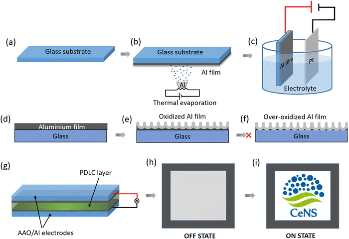 |
| | Fig. 1 Schematic illustration of (a–c) the deposition of the aluminium film and the anodization process setup, (d–f) the cross-sectional view of the Al film at different stages of the anodization process, (g) fabrication of the PDLC based smart window device using the anodized nanoporous aluminium (AAO/Al). (h) OFF or opaque state and (i) ON or transparent state of the PDLC smart window. | |
3.1. Optimization of the anodization voltage and morphological analysis of the anodized nanoporous aluminium (AAO/Al) TCE
The film uniformity, roughness, and structural morphology are strongly influenced by the anodization rate, which is managed by the voltage applied during the process. The above-mentioned parameters of the anodized films were investigated in detail using FESEM to identify the best suited voltage for the anodization, as shown in Fig. 2. The current density profile with the anodization time was also acquired at different anodization voltages ranging from 5 V to 50 V while keeping the electrolyte concentration and temperature fixed at 0.3 M and 25 ° C, respectively. FESEM images (Fig. 2a–c) show the morphology of the prepared anodized aluminium films. There is a noticeable roughness observed in the anodized films compared to the pristine Al film with a smooth surface (Fig. S1a, ESI†). In Fig. 2a, the Al-film anodized at a low voltage of 5 V shows tiny pores (diameter ∼10 nm) with high pore density. The pore diameter distribution in the anodized Al films at different voltages is provided in Fig. S2 (ESI†). Photographs (inset of Fig. 2a and c) of the anodized samples show no prominent reflection, which suggests that the top reflecting aluminium surface was converted into the transparent oxide during the anodization process. It was exceedingly challenging to regulate the transparency and conductivity of the anodized film at the low anodization voltage because the current density value at the cut-off region was very small. Additionally, as the anodization voltage increases, the pore size increases, and the related current density also rises. For 15 V and 50 V anodization voltages, pore size becomes approximately 20 nm and 30 nm (Fig. S2, ESI†), respectively. However, pore density is lower for 50 V anodization voltage than for 15 V (Fig. S3, ESI†). In the case of the higher anodization voltage (50 V), the anodization rate is very fast and ends up in creating non-uniform films. The FESEM images of the films at anodization voltages of 10 V, 30 V, and 40 V are also shown in Fig. S4 (ESI†). Additionally, the anodization voltages modify the inter-pore distance and hence decrease the pore density (Fig. S3, ESI†). This is supported by O’Sullivan et al. who have shown that the pore diameter (Dp) and interpore distance (Dint) between the two pores are directly proportional to the anodization potential,39 as shown by the equationwhere ζp is a constant and U is the applied anodization potential.
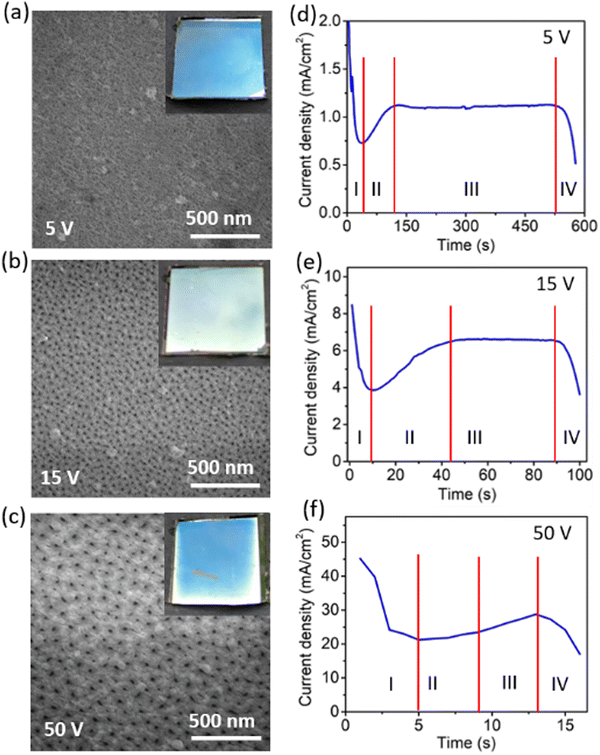 |
| | Fig. 2 FESEM images of the anodized nanoporous aluminium (AAO/Al) film at anodization voltages of (a) 5 V (b) 15 V and (c) 50 V. Inset images: photograph of the films, showing uniformity of the anodized film. Current density profile during anodization process at different applied anodization voltages of (d) 5 V (e) 15 V and (f) 50 V. | |
Furthermore, Ebihara et al. reported that Dint for oxalic acid is directly proportional to the anodization potential.40 However, the uniformity of the anodized film does not change with the anodization voltage of 15 V, as seen in the inset of Fig. 2b. Full photographs of the electrodes are shown in Fig. S5 (ESI†), which shows the grazing angle photographs capturing the reflection from the electrode surface. So, among the various anodization voltages, 15 V gives uniform anodized nanoporous aluminium (AAO/Al) films with good transparency and conductivity. The current response with time for different anodization voltages is shown in the Fig. 2d–f. The current response over time is divided into four stages for a fixed voltage. In stage-I, the current density drops suddenly from the high value to the minimum current value as the anodization process proceeds. The current density drop is ascribed to the barrier layer formation at the top of the aluminium film. The thickness of this barrier layer depends on the applied anodization voltage. When O2− ions come from the electrolyte, they react with Al3+ ions and form the barrier layer. Subsequently, at stage II, the Al3+ and O2− ions move at the metal/metal oxide interface and the interface of the metal/electrolytes, respectively. As anodization proceeds, the barrier starts dissolving due to the anodization voltage, which leads to the porous structure formation on the oxide layer. As the pore depth increases, the process maintains a constant current density (stage-III) until the pores come into contact with the substrate. The constant current density at stage III depends on the anodization voltage exponentially as,41,42
where,
Ip is the saturated current density (stage III),
Io is the constant current density that depends on the temperature,
a is a constant which depends on the concentration of the electrolyte, and V is the anodization voltage. The aluminium layer converts into the AAO layer in stage IV, when the pores come into contact with the substrate.
3.2. Anodization time variation
To obtain the Al nanoporous film beneath the AAO layer, the anodization process should be controlled by optimizing the anodization duration. However, prolonged anodization causes an over-oxidized Al film, and therefore makes a poorly conducting electrode. Fig. S6a (ESI†) shows the anodization current response for different anodization times at the anodization voltage of 15 V.
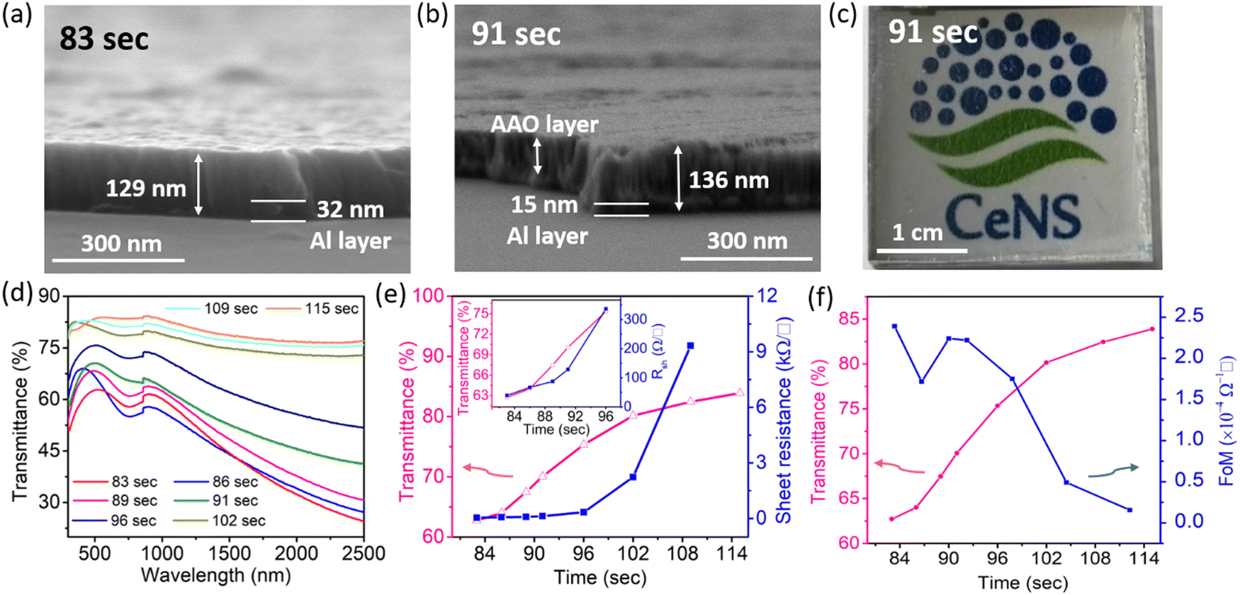
Fig. 3a shows the cross-sectional FESEM image of the sample for an anodization time of 83 s at 15 V anodization. As depicted, beneath the nanoporous AAO layer, a thick Al film of thickness ∼32 nm is still present, which although it results in a low sheet resistance, it suffers from poor transparency (Fig. 3e). A cross-sectional FESEM image of the anodized nanoporous aluminium (AAO/Al) TCE sample with an anodization time of 91 s is depicted in Fig. 3b. This AAO/Al sample has a very thin Al layer (≈15 nm) covered by an AAO layer (≈120 nm) that has good transparency with moderate sheet resistance (Fig. 3e). A photograph of the AAO/Al TCE is shown in Fig. 3c for the anodization time of 91 s, which confirms its good transparency. The XRD pattern of the AAO/Al TCE is shown in Fig. S6b (ESI†), which demonstrates the amorphous nature of the film, and which does not change significantly with the change of anodization times. The UV-Vis spectroscopy data that illustrates the increase in transparency with increased anodization times are shown in Fig. 3d, where the AAO/Al TCE transparency varies between 60% and 80% depending on the anodization periods (83 s and 115 s). Notably, the thin layer of Al beneath the AAO layer results in decreased transparency in the NIR band. The NIR radiation that Al metal reflects is the main factor reducing the NIR transparency. The transparency (at 550 nm) and sheet resistance (Rsh) of the AAO/Al TCE in response to the anodization time are shown in Fig. 3e. As the anodization time extends, the transparency and sheet resistance increases. It is evident that the transparency of the AAO/Al electrode increases to more than 82% after 102 s of anodization, degrading its conductivity and making it unsuitable for any optoelectronic applications (sheet resistance > 2.5 kΩ □−1). The complete conversion of Al film into AAO is responsible for the abrupt rise in the sheet resistance of the film after 102 s. Thus, for optoelectronic applications, 91 s can be considered as an optimal anodization time, which results in desired values of sheet resistance (128 Ω □−1) and transparency (70%). Furthermore, the figure of merit (FoM) is used to evaluate the performance of TCEs. FoM considers both optical transmittance and sheet resistance as important parameters. The ratio of optical conductivity (transmittance) to electrical conductivity (sheet resistance) is considered as the FoM to evaluate the performance of TCEs. Contextually, the figure of merit (FoM) for the electrode is calculated using Haacke's formula,43 defined as,
| |  | (3) |
where,
T is the transmittance at the wavelength 550 nm and
Rsh is the sheet resistance of the electrode.
Fig. 3f depicts the variation in transmittance and
FoM with various anodization times. Interestingly, it shows that the sample with the anodization duration of 91 s exhibits the highest
FoM of 2.22 × 10
−4 Ω
−1□.
 |
| | Fig. 3 FESEM cross-sectional images of the AAO/Al film at an anodization voltage 15 V at (a) 83 s (b) 91 s. (c) Photograph of the electrode for 91 s. (d) Optical transmittance spectra of the AAO/Al electrode at different anodization times. (e) Optical transmittance at 550 nm and sheet resistance variation of the AAO/Al film with the anodization times. Inset: rescaled representation of (e). (f) Optical transmittance and figure of merit (FoM) at different anodization times. | |
3.3. Stability and optical property analysis
Temperature and electrochemical stability tests were carried out on the optimized AAO/Al electrode to assess its viability in harsh environmental conditions. The nanoporous Al sheet is covered with an insulating AAO layer, which may help to keep the AAO/Al electrode stable. To better comprehend the effects of the AAO layer, the top AAO layer was removed using a wet chemical etching method (see the ESI†). The temperature stability comparison for the etched and unetched electrodes is shown in Fig. 4a–c. The data presented in Fig. 4a–c are recorded in the second cycle of the heating–cooling process between ambient temperature and 300 °C. According to Fig. 4a, the relative change in resistance (ΔR/R) increases linearly as the temperature rises to 300 °C for both electrodes. Fig. 4b depicts the ΔR/R at a constant applied temperature of 300 °C for one hour. It is noteworthy that the ΔR/R for both electrodes, i.e., (i) unetched – AAO/Al and (ii) etched – AAO/Al is nearly constant over the heating period, confirming their stability for higher temperature applications. Subsequently, the heater was turned off, and the ΔR/R of both electrodes were noted during the cooling process at different temperatures, as depicted in Fig. 4c. Notably, the electrode without etching attained almost its initial resistance value. Contrastingly, ΔR/R of the etched electrode did not attain its original value because the alumina (AAO) layer is thinner than the unetched electrode. As a result, when the temperature is applied, the top surface of the aluminium layer gets converted to the alumina layer, and the thickness of the aluminium layer drops, resulting in high resistance. Whereas, the AAO layer was present in the case of the unetched electrode, which prevented the further conversion of the bottom aluminium to alumina; as a result, after cooling down, the resistance change was noticeably low. However, the change in ΔR/R for the etched electrode was even more than the unetched electrode for the first cycle of the temperature stability test, as depicted in Fig. 4. Therefore, in the second cycle of the temperature stability test, no significant change was observed in the ΔR/R values for both electrodes (unetched and etched). To conclude, the AAO layer on top of the Al film enhances the temperature stability of the AAO/Al TCE.
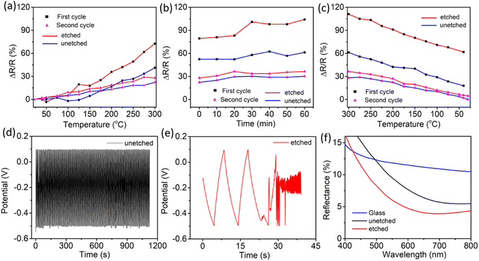 |
| | Fig. 4 Temperature stability test for the etched and unetched AAO/Al TCE. Relative change in resistance (ΔR/R) with increasing the temperature up to 300 °C (a), at the temperature 300 °C for 60 minutes (b), decreasing the temperature from 300 °C to ambient temperature (c). Electrochemical cyclic stability test for the unetched (d) and etched AAO/Al TCE (e). (f) Reflectance comparison between glass and the AAO/Al TCEs. | |
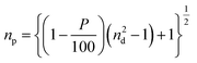
Further, to check the electrochemical stability of the AAO/Al electrode, we have conducted galvanostatic charge–discharge (GCD) as the electrochemical analysis (see the ESI†). The GCD curves for the unetched and etched AAO/Al TCE electrodes are shown in Fig. 4d and e, respectively. It is evident from the results that no degradation is observed in the electrochemical stability of the unetched electrode even after 100 cycles of charge–discharge, whereas the etched electrode has degraded just after two cycles. The electrochemical stability of the unetched electrode is attributable to the AAO layer on top of the aluminium nanopores, which helps to protect the AAO/Al electrode from erosion in harsh electrochemical conditions. This thin AAO layer is very much required for a thin aluminium layer as it has shallow electrochemical stability. In its pristine form, glass has a default nature to reflect a certain amount of optical light due to its smooth and planar surface. However, it is not desirable in specific applications. Therefore, an anti-reflection coating is desired on the glass surface. As porous structures exist in the AAO/Al TCE, which have the potential to serve as transparent anti-reflection coatings, the anti-reflection properties of these films can be adjusted by carefully controlling the etching time and optimising the size of the pores. These structures can support the employment of the AAO/Al electrodes as transparent conducting electrodes and anti-reflection coatings. The incident light can be trapped in the pores, rendering it incapable of returning from the surface. The amount of light getting trapped will vary depending on the pore size. The reflectance of the AAO/Al electrodes with various etching times is shown in Fig. 4f. It demonstrates that at 550 nm, the reflectance from plain glass without a coating is 11%, whereas the same for the unetched AAO/Al is only 5%. The reflectance decreased even further with the increase in etching time due to the changes in the pore size and spacing. The amount of trapped light increases as the porosity increases. The FESEM images of the unetched and etched AAO/Al electrodes are shown in Fig. S7a and b (ESI†). The variation in pore size with etching time is readily visible. As the etching time increased, the AAO pores grew wider and the space between them shrank, increasing the porosity of the AAO film. The refractive index of the film must be in-between that of the substrate and that of air for it to be anti-reflective. The refractive index of the film changes as its porosity increases. Yoldas et al. reported that the refractive index of the film depends on the porosity of the film as follows,44
| |  | (4) |
where,
np and
nd indicate the refractive indices of the porous and dense film.
P denotes the percentage of porosity present in the film. Therefore, the etched AAO/Al electrode has higher porosity value than the unetched AAO/Al resulting in a lower refractive index. As a result, the etched AAO/Al electrode has less reflectance compared to the unetched AAO/Al electrode.
Furthermore, the hydrophilic behaviour of the AAO/Al electrodes with the AAO layer in the unetched and etched samples was examined using the water contact angle (WCA) meter. According to Fig. S7c and d (ESI†), the rise in WCA from 8.9 to 15.9 degrees with longer etching times is attributable to an increase in surface energy. Additionally, we investigated the electrochemical impedance spectroscopy (EIS) for the unetched and etched AAO/Al electrodes (Fig. S8, ESI†). The phase angle in the low-frequency region of the bode plot is seen to increase with increasing etching time. This is directly related to the high capacitive behaviour for the high etching time as the AAO/Al electrode surface area increases with etching.
3.4. PDLC smart window
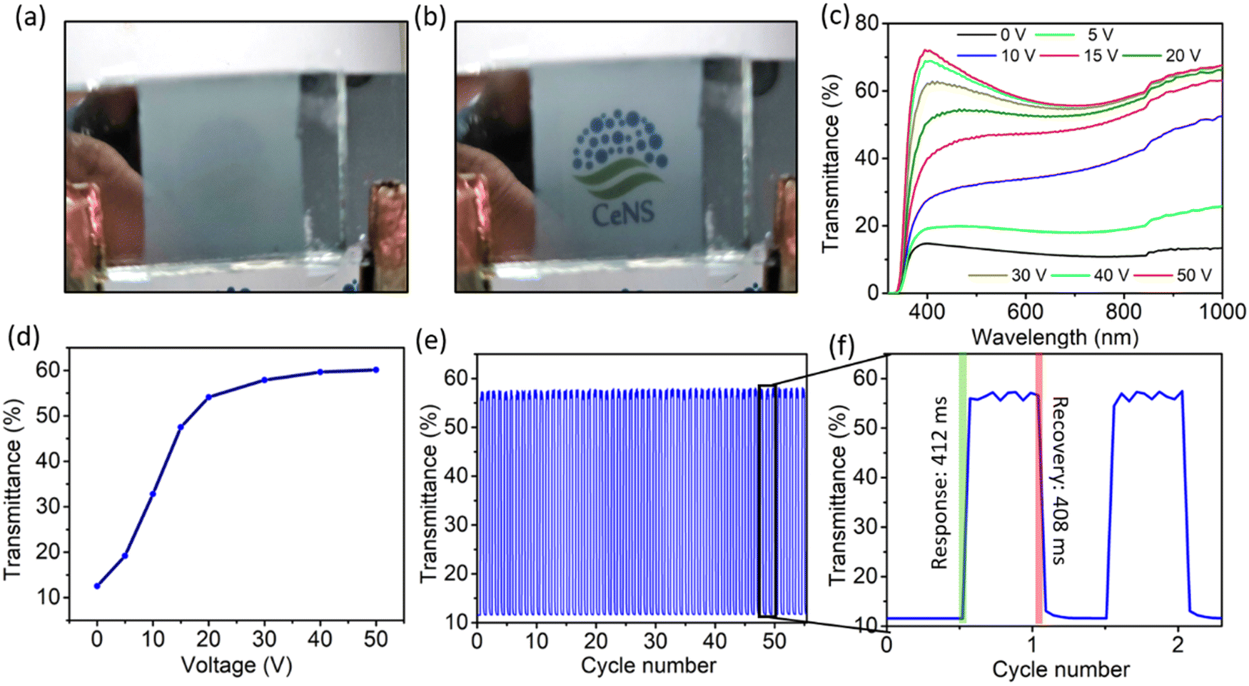
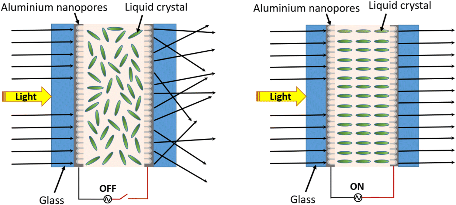
To demonstrate the applicability of the anodized nanoporous aluminium (AAO/Al) TCE, a polymer dispersed liquid crystal (PDLC) smart window device was fabricated by sandwiching the PDLC layer consisting of 60% NOA65 monomer and 40% liquid crystal between two AAO/Al electrodes with the support of 20 μm thick spacers. Photographs of the functional PDLC smart window device in its opaque (at 0 V) and transparent (at 50 V) states are shown in Fig. 5a and b, respectively. The electro-optical study was carried out at various applied voltages between 0 and 50 V, and the corresponding transparency was measured, as shown in Fig. 5c. When no voltage is applied (OFF state), it is observed that the transparency of the PDLC device is 12% at 550 nm. As the voltage increases, the transparency rises and reaches a value of 60% at 50 V. At 30 V, the transparency is nearly saturated at 54%, and subsequent voltage increases do not result in a discernible increase in transparency. Therefore, 30 V can be set as the working voltage of the device. Table S1 (ESI†) compares different threshold voltages among the various PDLC devices. Fig. 5d illustrates how the transmittance of the PDLC smart window changes with the increasing applied voltage from 0–50 V. The transmittance modulation of 44% and 42% are observed for the voltage of 50 V and 30 V, respectively, which again suggests that 30 V is sufficient for the optimized performance of the device. Fig. 5e shows the transmittance stability of the device over the ON–OFF cycle, which indicates no degradation in the transmittance modulation over 50 cycles. The response and recovery times of the PDLC-based device are shown in Fig. 5f, which are 412 ms and 408 ms, respectively. Additionally, the oxide layer on both AAO/Al electrodes further helps in preventing the risk of shorting the electrodes during operation. A schematic of the working mechanism of the PDLC smart window is shown in Fig. 6. At no applied voltage, since the liquid crystal particles are randomly oriented, they heavily scatter the incoming light to make the window opaque. The NOA65 monomer has a refractive index of 1.54 and the liquid crystal has a birefringent value of around Δn = 0.28 (ne = 1.81 and no = 1.53 where ne and no are the E-ray and O-ray refractive indices). When an electric field is applied, liquid crystal molecules are oriented along the field direction. As a result, the liquid crystal obtains the O-ray refractive index (no), which matches with that of NOA65. As a result, there is no scattering of light as it passes through the PDLC. Additionally, the porosity of the AAO film in the AAO/Al electrode would reduce its effective refractive index as described in eqn (4), matching it with the refractive index of NOA65 when light passes through the PDLC device, even though the bulk AAO layer has a refractive index of 1.77. Thus, the unique nanostructuring of the AAO/Al TCE effectively illustrates its benefit as a prospective transparent conducting electrode for optoelectronic applications.
 |
| | Fig. 5 Photograph of the (a) ‘OFF’ state and (b) ‘ON’ state of the PDLC smart windows with the AAO/Al electrode with an AC input voltage 0 V (OFF state) and 50 V (ON state). (c) UV-visible transmittance spectra of the PDLC smart window at different input AC voltages. (d) Transmittance (at 550 nm) of the PDLC smart window at different voltages. (e) Cycling stability test: transparency modulation in ON and OFF states of the device with the cycle number. (f) Response (OFF to ON) and recovery (ON to OFF) curves of the PDLC device. | |
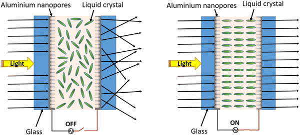 |
| | Fig. 6 Schematic of the PDLC mechanism, (a) liquid crystal particles are aligned when the power supply is ON and light passes through, (b) liquid crystal particles are randomly oriented when the power supply is OFF and light gets scattered. | |
4. Conclusion
The present work describes the fabrication of an affordable PDLC smart window device using a cost-effective anodized nanoporous aluminium (AAO/Al) transparent conducting electrode (TCE) developed through facile anodization of thin aluminium film deposited on a glass substrate. Various parameters such as voltage, time and chemical etching of the anodization process are optimized to develop a high-performance TCE. The developed AAO/Al TCE displayed transparency (T ∼ 70%), sheet resistance (Rsh ∼ 128 Ω □−1), electrochemical stability, and robustness in harsh environmental conditions (temp. > 300 °C) along with anti-reflection features due to nanoporous structures. Further, a two-terminal PDLC smart window device (size ∼ 3 × 2 cm2) was fabricated, which operates at 30 V only with a transparency modulation of ∼45%. This study indicates that the anodized nanoporous aluminium (AAO/Al) TCE could replace the existing TCEs used in PDLC smart windows.
Conflicts of interest
There are no conflicts to declare.
Acknowledgements
The authors are grateful to Professor C. N. R. Rao for his encouragement. The authors thank Professor G. U. Kulkarni for discussion and input. The financial support from the department of science and technology (DST), Government of India (project grant no. DST/TDT/AMT/2021/009), is gratefully acknowledged. The authors acknowledge Mr Mukhesh K G for helping to operate the thermal evaporation system and for discussion. The authors acknowledge ‘JNCASR, Bengaluru’ and ‘CeNS, Bengaluru’ for the Central research laboratory facilities. R. R. and I. M. acknowledge CSIR (09/1243(0005)/2021-EMR-I) and JNCASR, respectively, for fellowships.
References
- Y. Ke, I. Balin, N. Wang, Q. Lu, A. I. Y. Tok, T. J. White, S. Magdassi, I. Abdulhalim and Y. Long, ACS Appl. Mater. Interfaces, 2016, 8, 33112–33120 CrossRef CAS PubMed.
- Y. Ke, Y. Yin, Q. Zhang, Y. Tan, P. Hu, S. Wang, Y. Tang, Y. Zhou, X. Wen, S. Wu, T. J. White, J. Yin, J. Peng, Q. Xiong, D. Zhao and Y. Long, Joule, 2019, 3, 858–871 CrossRef CAS.
- Y. Cui, Y. Ke, C. Liu, Z. Chen, N. Wang, L. Zhang, Y. Zhou, S. Wang, Y. Gao and Y. Long, Joule, 2018, 2, 1707–1746 CrossRef CAS.
- S. Bi, C. Feng, M. Wang, M. Kong, Y. Liu, X. Cheng, X. Wang and X. Chen, Carbohydr. Polym., 2020, 229, 115557 CrossRef CAS PubMed.
- M. Aburas, V. Soebarto, T. Williamson, R. Liang, H. Ebendorff-Heidepriem and Y. Wu, Appl. Energy, 2019, 255, 113522 CrossRef.
- Y. Gao, S. Wang, H. Luo, L. Dai, C. Cao, Y. Liu, Z. Chen and M. Kanehira, Energy Environ. Sci., 2012, 5, 6104–6110 RSC.
- J. L. Wang, S. Z. Sheng, Z. He, R. Wang, Z. Pan, H. Y. Zhao, J. W. Liu and S. H. Yu, Nano Lett., 2021, 21, 9976–9982 CrossRef CAS PubMed.
- L. Wang, Y. Liu, X. Zhan, D. Luo and X. Sun, J. Mater. Chem. C, 2019, 7, 8649–8654 RSC.
- A. K. Singh, S. Kiruthika, I. Mondal and G. U. Kulkarni, J. Mater. Chem. C, 2017, 5, 5917–5922 RSC.
- Z. Xie, X. Jin, G. Chen, J. Xu, D. Chen and G. Shen, Chem. Commun., 2014, 50, 608–610 RSC.
- P. Lemarchand, J. Doran and B. Norton, Energy Procedia, 2014, 57, 1878–1887 CrossRef.
- I. Mondal, S. Kiruthika, M. K. Ganesha, M. Baral, A. Kumar, S. Vimala, P. L. Madhuri, G. G. Nair, S. K. Prasad, A. K. Singh and G. U. Kulkarni, J. Mater. Chem. A, 2021, 9, 23157–23168 RSC.
- R. Baetens, B. P. Jelle and A. Gustavsen, Sol. Energy Mater. Sol. Cells, 2010, 94, 87–105 CrossRef CAS.
- S. Kumar, D. Kang, V. H. Nguyen, N. Nasir, H. Hong, M. Kim, D. C. Nguyen, Y. J. Lee, N. Lee and Y. Seo, ACS Appl. Mater. Interfaces, 2021, 13, 40976–40985 CrossRef PubMed.
- S. Kumar, H. M. Park, V. H. Nguyen, M. Kim, N. Nasir, M. Kumar and Y. Seo, Ceram. Int., 2022, 48, 35092–35099 CrossRef CAS.
- M. F. Al-Kuhaili, J. Mater. Sci.: Mater. Electron., 2020, 31, 2729–2740 CrossRef CAS.
- C. Bianchi, A. C. Marques, R. C. da Silva, T. Calmeiro and I. Ferreira, Sci. Rep., 2021, 11, 1–11 CrossRef PubMed.
- Z. X. Lim and K. Y. Cheong, Phys. Chem. Chem. Phys., 2015, 17, 26833–26853 RSC.
- D. Ko, B. Gu, S. J. Kang, S. Jo, D. C. Hyun, C. S. Kim and J. Kim, J. Mater. Chem. A, 2019, 7, 14536–14544 RSC.
- F. Xu, W. Xu, B. Mao, W. Shen, Y. Yu, R. Tan and W. Song, J. Colloid Interface Sci., 2018, 512, 208–218 CrossRef CAS PubMed.
- I. Mondal, G. Bahuguna, M. K. Ganesha, M. Verma, R. Gupta, A. K. Singh and G. U. Kulkarni, ACS Appl. Mater. Interfaces, 2020, 12, 54203–54211 CrossRef CAS PubMed.
- S. Walia, I. Mondal and G. U. Kulkarni, ACS Appl. Electron. Mater., 2021, 1, 1597–1604 CrossRef.
- Y. G. Seol, T. Q. Trung, O. J. Yoon, I. Y. Sohn and N. E. Lee, J. Mater. Chem., 2012, 22, 23759–23766 RSC.
- C. Zhan, G. Yu, Y. Lu, L. Wang, E. Wujcik and S. Wei, J. Mater. Chem. C, 2017, 5, 1569–1585 RSC.
- C. Y. Su, A. Y. Lu, Y. L. Chen, C. Y. Wei, C. H. Weng, P. C. Wang, F. R. Chen, K. C. Leou and C. H. Tsai, J. Phys. Chem. C, 2010, 114, 11588–11594 CrossRef CAS.
- Y. Zhou and R. Azumi, Sci. Technol. Adv. Mater., 2016, 17, 493–516 CrossRef CAS PubMed.
- Y. S. Woo, Micromachines, 2019, 10, 24–28 Search PubMed.
- X. Wang, D. Zhang, H. Jin, B. Z. Poliquit, B. Philippa, R. C. R. Nagiri, J. Subbiah, D. J. Jones, W. Ren, J. Du, P. L. Burn and J. Yu, Sol. RRL, 2019, 3, 1–10 Search PubMed.
- C. John Zhang and V. Nicolosi, Energy Storage Mater., 2019, 16, 102–125 CrossRef.
- S. Bai, X. Guo, T. Chen, Y. Zhang, X. Zhang, H. Yang and X. Zhao, Composites, Part A, 2020, 139, 106088 CrossRef CAS.
- J. Yun, Adv. Funct. Mater., 2017, 27, 1606641 CrossRef.
- S. Kiruthika, K. D. M. Rao, A. Kumar, R. Gupta and G. U. Kulkarni, Mater. Res. Express, 2014, 1, 026301 CrossRef CAS.
- R. K. Govind, I. Mondal, K. Baishya, M. K. Ganesha, S. Walia, A. K. Singh and G. U. Kulkarni, Adv. Mater. Technol., 2022, 7, 1–8 Search PubMed.
- L. Zaraska, G. D. Sulka, J. Szeremeta and M. Jaskuła, Electrochim. Acta, 2010, 55, 4377–4386 CrossRef CAS.
- A. P. Leontiev, I. V. Roslyakov and K. S. Napolskii, Electrochim. Acta, 2019, 319, 88–94 CrossRef CAS.
- G. D. Sulka and W. J. Stepniowski, Electrochim. Acta, 2009, 54, 3683–3691 CrossRef CAS.
- Y. Li, Y. Chen, M. Qiu, H. Yu, X. Zhang, X. W. Sun and R. Chen, Sci. Rep., 2016, 6, 1–7 CrossRef PubMed.
- S.
Z. Chu, K. Wada, S. Inoue and S. Todoroki, J. Electrochem. Soc., 2002, 149, B321 CrossRef CAS.
- J. P. O’Sullivan and G. C. Wood, Proc. R. Soc. London, Ser. A, 1970, 317, 511–543 Search PubMed.
- K. Ebinara, H. Takahashi and M. Nagayama, J. Surf. Finish. Soc. Jpn., 1982, 33, 156–164 Search PubMed.
- A. M. Abd-Elnaiem and A. Gaber, Int. J. Electrochem. Sci., 2013, 8, 9741–9751 CAS.
- W. Lee and S. J. Park, Chem. Rev., 2014, 114, 7487–7556 CrossRef CAS PubMed.
- G. Haacke, J. Appl. Phys., 1976, 4086, 1–5 Search PubMed.
- B. E. Yoldas and D. P. Partlow, Thin Solid Films, 1985, 129, 1–14 CrossRef CAS.
|
| This journal is © The Royal Society of Chemistry 2023 |
Click here to see how this site uses Cookies. View our privacy policy here. 
 Open Access Article
 This Open Access Article is licensed under a
  ab,
Indrajit
Mondal
ab,
Indrajit
Mondal