
 Open Access Article
 This Open Access Article is licensed under a Creative Commons Attribution-Non Commercial 3.0 Unported Licence
A highly sensitive and miniaturized wearable antenna based on MXene films for strain sensing†
Ao
Yin
ab,
Chen
Zhang
*ab,
Jingjing
Luo
ab,
Jiang
Liu
ab,
Zhongqi
Ren
 ab,
Yuxin
Wang
ab,
Yang
Ye
ab,
Rui
Yin
ab,
Qiang
Feng
ab,
Youyou
Chen
abc,
Kang
Li
ab,
Weiwei
Zhao
*abc,
Suzhu
Yu
*ab and
Jun
Wei
*abc
ab,
Yuxin
Wang
ab,
Yang
Ye
ab,
Rui
Yin
ab,
Qiang
Feng
ab,
Youyou
Chen
abc,
Kang
Li
ab,
Weiwei
Zhao
*abc,
Suzhu
Yu
*ab and
Jun
Wei
*abc
aShenzhen Key Laboratory of Flexible Printed Electronics Technology, Harbin Institute of Technology (Shenzhen), Shenzhen 518055, People's Republic of China. E-mail: zhangchen2020@hit.edu.cn; wzhao@hit.edu.cn; junwei@hit.edu.cn
bSauvage Laboratory for Smart Materials, School of Materials Science and Engineering, Harbin Institute of Technology (Shenzhen), Shenzhen 518055, People's Republic of China
cState Key Laboratory of Advanced Welding & Joining, Harbin Institute of Technology, Harbin 150001, People's Republic of China
First published on 19th December 2022
Abstract
With the prosperous development of wearable electronics, flexible radio-frequency wireless antenna sensors have attracted considerable interest due to their various applications in the Internet of things (IoT). However, vital issues including device configurations and materials restricted the miniaturization and flexibility of antenna sensors. In this work, we demonstrated a microstrip antenna wireless sensor consisting of a copper ground plane, a polydimethylsiloxane dielectric substrate and an MXene patch. Our optimized device possessed a small size (40 × 40 mm2) with a resonant frequency at 4.8 GHz and a frequency-shift range of 8% under different strains and matches well with 5G communications. Moreover, our antenna wireless sensor exhibited excellent mechanical flexibility and stable response to repetitive stimulations. The strain sensitivity of 20 is also impressive among similar antenna sensors. The demonstrations on human body and cantilever motion monitoring were conducted with desirable stability and sensitivity, where the sensor showed obvious shifted resonant frequencies while the reflection coefficient was maintained at around −25 dB, revealing its great potential in healthcare monitoring, construction diagnosis and IoT.
1. Introduction
In recent years, wearable and flexible electronics have gained increasing attention in the industrial and academic world.1–3 The mechanical properties of flexible electronics involve wrinkling, bending, and stressing, which would considerably extend the applications of modern electronic devices to multiple non-flat scenarios, including the human body.4,5 To bear the complicated application environment, the research of emerging smart, multifunctional, refined sensors with properties such as excellent instantaneity, flexibility and compatibility has become a hot topic. With such development in flexible sensors and the booming evolution of IoT (Internet of Things), our life would be technologically upgraded for more convenience.6,7Among the various sensing devices, microstrip patch antenna sensors have been a research focus due to their simple configuration, multimodality sensing ability, passive operation, and low cost.8–10 A microstrip patch antenna sensor is an electronic device with dual functionality of communicating and sensing, which can reduce the number of components and thus the fabrication procedures. The working principle of this antenna sensor is that its geometrical and/or dielectric constant variation would result in the corresponding antenna resonance frequency shift.11,12 For example, Cheng and colleagues designed meshed and arched microstrip antenna-based strain sensors, whose resonance frequency at external tensile strain followed reverse rules due to their different structures, and the arched antenna sensors exhibited high sensitivity for human wrist monitoring.13 However, the sensitivity improvement of the antenna sensor is limited if relying solely on the optimization of the antenna structure.
The application of novel materials in microstrip antenna sensors is also extremely crucial to enhance the sensor performance. Metals are commonly used in the existing commercial radio frequency sensors. However, these materials suffer from not only poor flexibility, high density, and easy corrosion but also skin depth restriction,14–17 which hinder their long-term and large-scale applications. In recent years, conductive polymers and carbon materials such as carbon nanotubes and graphene have attracted wider attention.18–20 Compared to metals, these materials are endowed with properties such as light weight and great flexibility at the sacrifice of conductivity. Currently, MXenes, a class of novel 2D materials, are reported as a potential choice. MXenes possess unique superiorities such as outstanding electrical conductivity, large specific surface area, unique layered-structure, excellent dispersibility in aqueous solutions and abundant terminal groups, endowing them with great application potency to construct highly sensitive antenna sensors with large-scale manufacturing convenience.20–23
In this work, we demonstrated a small-sized (40 × 40 mm2) microstrip antenna wireless sensor, which consists of a conductive MXene patch, a polydimethylsiloxane (PDMS) dielectric layer and a copper ground plane. The antenna stimulates the radiation field between the patterned MXene and the copper ground, and radiates outward through the gap. Once the antenna deforms, the changing conductivity of the MXene will have an effect on the resonant frequency of the antenna. Different from the traditional rectangular patch antenna, we designed a round patch antenna and sacrificed the gain of the antenna, but it can further reduce the size of the antenna. The round patch means that there are less time-changing current and weaker radiation fields, which leads to a reduction in gain, but the variation characteristics of the resonant frequency of the antenna will not change, which can be used as the sensor. The optimized device showed a resonant frequency at 4.8 GHz with an 8% shifting range under strain stimulation, which is within the 5G communication domain. Meanwhile, our antenna wireless sensor exhibited excellent flexibility, ensuring its conformable attachment and mechanical stability. Practical applications including human movement and cantilever monitoring were also demonstrated with desirable sensitivity and repeatability. This work may provide inspiration for the designing of portable, flexible and wearable antenna sensors for wide applications such as e-skins, intelligent human–machine interfaces and artificial prosthetics.
2. Experimental
2.1. Preparation of the MXene film patch
Firstly, the etchant solution was prepared by adding 1 g of LiF in 20 mL of 9 M HCl. Secondly, 1 g of MAX phase precursor (Ti3AlC2) was added to the etchant solution, and the etching reaction proceeded at 35 °C for 24 h. Thirdly, the acidic solution was washed using deionized water via centrifugation at 3500 rpm for 4 times. When the solution pH > 6, the supernatant was decanted. Then the as-obtained sediment was mixed with deionized water and shaken for 30 min to delaminate the Ti3C2 flakes. After about 1 h of centrifugation at 3500 rpm, the MXene dispersion was obtained from the supernatant. Then prepare PDMS by mixing component A and curing agent B at a ratio of 10![[thin space (1/6-em)]](https://www.rsc.org/images/entities/char_2009.gif) :1. To accelerate the commixture, the blend was ultrasonically treated for 15 min under an ice bath. Then the compound was transferred into a vacuum oven for 12 h at room temperature to wipe off the bubbles. Then the MXene dispersion of an optimized concentration at 5 mg mL−1 was spray-coated via a 500 μm nozzle on the plasma-hydrophilized PDMS substrate, which was covered with a mask and heated at 150 °C to obtain an intact film. The spray gun was set at an angle of 45° and a distance of 40 cm to the PDMS substrate.
:1. To accelerate the commixture, the blend was ultrasonically treated for 15 min under an ice bath. Then the compound was transferred into a vacuum oven for 12 h at room temperature to wipe off the bubbles. Then the MXene dispersion of an optimized concentration at 5 mg mL−1 was spray-coated via a 500 μm nozzle on the plasma-hydrophilized PDMS substrate, which was covered with a mask and heated at 150 °C to obtain an intact film. The spray gun was set at an angle of 45° and a distance of 40 cm to the PDMS substrate.
2.2. Design of the antenna
The resonant frequency of the antenna is designed to be at 4.8 GHz to meet the requirements of 5G mobile communication for antennas. The electromagnetic field characteristics of the antenna are analyzed by the transmission line model method, and the physical parameters of the antenna are designed according to the following equations:24 | (1) |
 | (2) |
2.3. Device fabrication
The PDMS substrate acting as the dielectric layer was sandwiched between the copper ground and MXene patch, and the feed line was also prepared with MXene dispersion. After that, an industrial wire combined with a Sub-Miniature-A (SMA) was welded with the sandwiched structure by a silver agent solidified at 100 °C for 1 h.2.4. Characterization
The surface morphology of the MXene film was measured by scanning electron microscopy (SEM, HITACHI S-4700), and the cross-section was observed using an SEM of ZEISS SUPRA-55. X-ray diffraction (XRD) patterns were recorded using an X-ray diffractometer (Aries). And the radiation signal was measured using a Rohde & Schwarz vector network analyzer (VNA).3. Results and discussion
The fabrication routes of devices are shown in Fig. 1a. After HCl/LiF etching, the bulky MAX phase Ti3AlC2 was transferred to delaminated Ti3AlC2 deliberately. Then the suspension was washed with deionized water to decrease the acidity before being preserved in the centrifuge tube. The PDMS substrate was treated with O2 plasma to convert the C–H bonds to hydrophilic carboxy groups to improve its interaction with the MXene. An optimized substrate temperature of 150 °C was set to facilitate the evaporation of the solvent and minimize the coffee-ring effect, thus obtaining a uniform and intact MXene film. Fig. 1b shows the equivalent circuit of the antenna sensor, where YC is the characteristic admittance of the microstrip patch and GS is the slit radiation admittance. The deformed patch has a remarkable impact on the slit radiation admittance. Fig. 1c illustrates the working principle of the wireless passive sensing system. Firstly, the flexible antenna sensor was conformably attached to the human body (e.g., elbows, fingers, etc.) and both weeny or drastic body motions would result in antenna deformation. Meanwhile, the radiation parameters changed accordingly, which could be detected by the VNA. After analyzing the received radiation data, the body motion information could be concluded. | ||
| Fig. 1 (a) The preparation of the MXene suspension and the modified PDMS substrate with the plasma process. (b) The equivalent circuit diagram of the antenna sensor and the photograph of the fabricated antenna sensor. (c) Schematic illustration for the principle of the sensor to monitor human motion. (d) The data were collected using a vector network analyzer (VNA). | ||
The morphology of the MXene film is illustrated in Fig. 2a. The MXene flakes (20–100 μm in diameter) stack layer by layer in contiguous domain zones to construct the conducting pathway, yielding an MXene film of low sheet resistance. Fig. 2b shows the cross-sectional view of the film, whose thickness is only around 5 μm. Therefore, a high conductivity of ∼200 S cm−1 was calculated, leading to a low electromagnetic wave loss. Fig. 2d demonstrates the cross-sectional morphology of the curving film. The MXene flakes maintained a tight connection as a whole, with a slight local crowning in the bending center. The strain mismatch between the MXene and the substrate leads to an adjustable interspace, whose variation would affect the charge transfer pathway and the slit radiation admittance. Fig. 2c displays a magnified view of the curved MXene film with obvious wrinkles caused by upheaval flakes, resulting in an altered conductive pathway. Both the interspace and the wrinkles would contribute to the high sensitivity of the antenna sensor (as will be discussed later). In addition, XRD patterns of the MXene films are shown in Fig. 2e. The freshly made sample displays classical diffraction peaks at 6.6°, confirming the successful preparation of the MXene with an interlayer spacing of ∼15 Å.25 After deformation and 21 days of storage under ambient conditions, the sample reveals slightly left-shifted peaks, which is contrary to the right-shift on oxidation.26 This is due to the increased interlayer space caused by film deformation, and validates no oxidation occurring. Then the photographs of the antenna sensor in flat, curving, tortuous, and rolled states are shown in Fig. 2f, indicating its excellent flexibility and potential for practical use.
 | ||
| Fig. 2 The micro-morphology and the macro-profile of the antenna sensor and its compression/tension sensitivity. SEM images of (a) the surface and (b) the cross-section of the device under the flat state, and (c) the surface and (d) the cross-section of the device under the bending state. (e) XRD patterns of the MXene film as freshly made and after storage for 21 days in air. (f) Photographs of the flexible antenna sensor in flat, curving, tortuous, and rolled states. | ||
Fig. 3 reveals the theoretical size optimization and practical evaluation of the antenna sensor. The current distribution of the antenna could be tuned by placing a patch layer on the dielectric layer, where the input impedance of the antenna can be distributed according to the transmission line model, and the size of the antenna can be decreased by increasing the relative permittivity, which is a commonly adopted method for antenna miniaturization.27 According to electromagnetic theory, a certain electromagnetic resonant cavity would form between the radiating element and the metal grounding plate. When the microwave signal excites the microstrip antenna, it will excite the radio frequency electromagnetic field to resonate and pass through the gap between the radiating element and the metal ground plate.28 The antenna radiation properties can be characterized by the reflection coefficient (S11). For example, the reflection coefficient curve of a typical antenna is shown in Fig. 3a and b. At the resonant frequency of the antenna sensor, the return loss is the largest, so that the reflection coefficient curve reaches the bottom at the resonant frequency. A substrate thickness of 0.5 mm displayed the lowest electromagnetic loss (Fig. 3a). Under the optimized thickness, we further optimized the patch radius to be 12.5 mm (Fig. 3b).
 | ||
| Fig. 3 The theoretical size optimization and experimental evaluation of the antenna sensor. The simulation of reflection coefficient as a function of (a) the substrate thickness h and (b) the patch radius r. The simulation results of (c) compressing states in different angle versus resonant frequency and (d) Smith chart related with impedance matching. The experimental results of reflection coefficient under (e) resonant frequency and reflection coefficient versus patch radius (f) tensile states versus resonant frequency. | ||
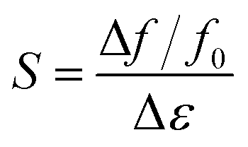
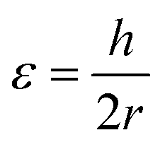
According to Fig. 3c, the resonant frequency decreases from 5.8 GHz to 4.3 GHz as the patch radius expands, while S11 demonstrates the minimum value at r = 12.5 mm with the resonant frequency of 4.8 GHz, which corresponds to the 5G communication requirements. As a result, we chose the optimized size (h = 0.5 mm and r = 12.5 mm) for the following antenna sensor research. Fig. 3d shows an excellent resistance match according to the simulated Rx (1.0076 + 0.0093i), which is close to 1. Moreover, the resonant frequency will shift when the antenna sensor is under the deformed state, as shown in Fig. 3e and f. Specifically, the resonant frequency of the sensor increases with the rising curvature radius (r′), either the sensor is compressed or stretched. The sensitivity S of our sensor under the bending state is calculated by the following formulation:
 | (3) |
 | (4) |
| Materials | Substrate | Size (mm) | Resonant frequency (GHz) | Max sensitivity (a.u.) | Ref. |
|---|---|---|---|---|---|
| Al | ABS | 17.5 × 3.5 | 5.54 | 17 | 28 |
| Shiled conductor | Felt | 24.26 × 66.58 | 1.78 | 1.25 | 29 |
| Graphene | Cellulose filter paper | 65.2 × 13 | 1.6 | 9.8 | 9 |
| Al | Cellulose filter paper | 29.5 × 37.7 | 2.45 | 3.49 | 8 |
| Silver | Polyester | 43.5 × 50.3 | 2.48 | — | 30 |
| Silver | PET | 48.5 × 70.82 | 2.42 | — | 32 |
| Conductive fabric | PDMS | 22.6 × 35.6 | 2.45 | 33 | |
| EGaIn | PDMS | 20 × 24 | 3.45 | 8.3 | 11 |
| Copper | PI | 140 × 150 | 1.5 | — | 34 |
| Silver-plated nylon yarn | Cotton | 2.25 | 4.02 | 35 | |
| MXene | PDMS | Φ25 | 4.92 | 19.23 | This work |
Fig. 4a–c. illustrates the body motion detection signals of the antenna sensor. The red line in Fig. 4a representing the elbow sensor showed a distinct variation amplitude from ∼91% to ∼100%, while the black line displaying the hand sensor shows a slightly narrow variation range of ∼97% to 101%. As shown in Fig. 4a and b, when the fist was flat, the sensor was in its original state with the resonant frequency at 4.8 GHz. Once the fist was clenched, the antenna sensor immediately responded in the form of the shifting resonant frequency due to the PDMS substrate deformation. Similarly, by attaching the antenna sensor to the inside of the elbow, we can monitor the elbow motion through the changing S11 signal (Fig. 4a and c). Both the body sensors showed repeatable output signals, which is essential for reliable daily applications as motion sensors.
 | ||
| Fig. 4 Application of the antenna strain sensor. (a) Sensing signals of different human body motions: (black line) clenching fist and relaxing repeatedly, and (red line) bending the elbow and relaxing repeatedly. Photographs of (b) hand/fist sensing and (c) elbow sensing with our antenna sensor. (d) Normalized frequency changing with the stretching state and bending state and (e) the deformation of a small scale at the compress state and (f) tensile state. (g) Micro-strain detection with our antenna acting as a strain sensor for a cantilever plate. (h) The variation of resonant frequency and reflection coefficient under different mass weights (i) Fitted curve of resonant frequency versus strain. | ||
Apart from the body motion sensor, our antenna sensor can also be applied in precise conditions such as medical and surgical fixation, high precision mechanical equipment and construction measurement. For these applications, stability and reliability are of great importance. Thus, we fixed the device on a foam substrate; once we stimulate the foam with a tough cuspidal tool which was common in the lab, the sensor would respond immediately. Fig. 4d shows the response signals under different stimulations. The positions −1 and −3 represent the force that was given from the back side of the antenna sensor (Fig. 4e), positions 1 and 3 represent the stimulation that was applied on the front side (Fig. 4f), and positions 0 and ±2 are the original state with no external stimulations. The obvious and periodic shifting in Fig. 4d revealed its fast response and stable cyclical characteristic as a potential crack sensor. Actually, our sensor could monitor not only large movements, but also exquisite deformations. For example, Fig. 4g is an illustration of a typical metal cantilever plate, and our antenna could monitor the strain of the cantilever. The cantilever plate is made of 1060 aluminum. One end of the cantilever plate is fixed with a C-type clamp, and the strain is produced by applying a load through a suspended weight at the free end of the plate on the other side. The sensor is bonded to the cantilever plate while the load is applied along the length direction of the radiating element. By loading different weights, the stress of the cantilever as well as the antenna sensor would be changed, together with the antenna resonant frequency (Fig. 4h). It is noteworthy that the loading weights have been carefully set between 0 and 120 g in our case to obtain a satisfactory strain variation without damaging the cantilever. Fig. 4h shows that the resonant frequency decreased with the increasing strain. For example, at the loading weight of 0, 60 and 120 g, the resonant frequency decreased gradually from 4.91, 4.76, to 4.64 GHz, respectively. And the sensitivity was calculated to be 425 kHz/με with a linearity of 0.98. Therefore, the wireless antenna sensor demonstrates an expected property for applications as a metal strain monitor.
4. Conclusions
In summary, we demonstrated a wearable wireless microstrip patch antenna sensor based on an MXene film with excellent sensitivity and flexibility. In particular, the radiation results measured by the VNA were well consistent with theoretical simulations, and showed promising prospects for 5G communication. Additionally, we conducted a series of measurements on its detecting capabilities in compression and tensile situations while also keeping an eye on limb movements and preparing it as a wireless metal strain sensor. The up to 20 sensitivity is impressive among the related antenna sensors and the excellent flexibility revealed the great potential for application in healthcare monitoring, construction diagnosis and IoT. However, the PDMS substrate and the connected wires affect the radiation efficiency to some degree, which should be further improved in future work. The reported fabrication routes and materials could be applied in other complex flexible antenna sensors with designed patterns.Conflicts of interest
There are no conflicts to declare.Acknowledgements
This work was financially supported by the Shenzhen Science and Technology Program (Grant No. KQTD20200820113045083 and ZDSYS20190902093220279).References
- F. R. Fan, W. Tang and Z. L. Wang, Adv. Mater., 2016, 28, 4283–4305 CrossRef.
- Z. Lou, L. Wang, K. Jiang, Z. Wei and G. Shen, Mater. Sci. Eng., R, 2020, 140, 100523 CrossRef.
- R. Feiner and T. Dvir, Nat. Rev. Mater., 2018, 3, 17076 CrossRef CAS.
- Y. Ma, Y. Zhang, S. Cai, Z. Han, X. Liu, F. Wang, Y. Cao, Z. Wang, H. Li, Y. Chen and X. Feng, Adv. Mater., 2020, 32, 1902062 CrossRef CAS.
- M. Kaltenbrunner, T. Sekitani, J. Reeder, T. Yokota, K. Kuribara, T. Tokuhara, M. Drack, R. Schwödiauer, I. Graz, S. Bauer-Gogonea, S. Bauer and T. Someya, Nature, 2013, 499, 458–463 CrossRef CAS PubMed.
- R. C. Webb, A. P. Bonifas, A. Behnaz, Y. Zhang, K. J. Yu, H. Cheng, M. Shi, Z. Bian, Z. Liu, Y.-S. Kim, W.-H. Yeo, J. S. Park, J. Song, Y. Li, Y. Huang, A. M. Gorbach and J. A. Rogers, Nat. Mater., 2013, 12, 938–944 CrossRef CAS.
- A. Sarycheva, A. Polemi, Y. Liu, K. Dandekar, B. Anasori and Y. Gogotsi, Sci. Adv., 2018, 4, eaau0920 CrossRef.
- S. Kanaparthi, V. R. Sekhar and S. Badhulika, Extreme Mech. Lett., 2016, 9, 324–330 CrossRef.
- K. Kwon, J. U. Kim, Y. Deng, S. R. Krishnan, J. Choi, H. Jang, K. Lee, C.-J. Su, I. Yoo, Y. Wu, L. Lipschultz, J.-H. Kim, T. S. Chung, D. Wu, Y. Park, T. Kim, R. Ghaffari, S. Lee, Y. Huang and J. A. Rogers, Nat. Electron., 2021, 4, 302–312 CrossRef.
- K. K. Kazemi, T. Zarifi, M. Mohseni, R. Narang, K. Golovin and M. H. Zarifi, ACS Appl. Mater. Interfaces, 2021, 13, 34877–34888 CrossRef CAS.
- G. J. Hayes, Ju-Hee So, A. Qusba, M. D. Dickey and G. Lazzi, IEEE Trans. Antennas Propag., 2012, 60, 2151–2156 Search PubMed.
- M. Selvaggio, L. A. Ramirez, N. D. Naclerio, B. Siciliano and E. W. Hawkes, in 2020 IEEE International Conference on Robotics and Automation (ICRA), IEEE, Paris, France, 2020, pp. 3227–3233.
- J. Zhu, J. J. Fox, N. Yi and H. Cheng, ACS Appl. Mater. Interfaces, 2019, 11, 8867–8877 CrossRef CAS PubMed.
- M. Ren, Y. Zhou, Y. Wang, G. Zheng, K. Dai, C. Liu and C. Shen, Chem. Eng. J., 2019, 360, 762–777 CrossRef CAS.
- S. Parandeh, M. Kharaziha and F. Karimzadeh, Nano Energy, 2019, 59, 412–421 CrossRef CAS.
- H. Zhang, X. Sun, M. Hubbe and L. Pal, ACS Appl. Electron. Mater., 2019, 1, 1179–1188 CrossRef CAS.
- Y. Wang, L. Zhu, D. Mei and W. Zhu, J. Mater. Chem. C, 2019, 7, 8669–8679 RSC.
- J. Zhang, R. Song, X. Zhao, R. Fang, B. Zhang, W. Qian, J. Zhang, C. Liu and D. He, ACS Omega, 2020, 5, 12937–12943 CrossRef CAS.
- J. Chen, Q. Yu, X. Cui, M. Dong, J. Zhang, C. Wang, J. Fan, Y. Zhu and Z. Guo, J. Mater. Chem. C, 2019, 7, 11710–11730 RSC.
- Q. Guo, X. Zhang, F. Zhao, Q. Song, G. Su, Y. Tan, Q. Tao, T. Zhou, Y. Yu, Z. Zhou and C. Lu, ACS Nano, 2020, 14, 2788–2797 CrossRef CAS.
- D. Wang, L. Wang, Z. Lou, Y. Zheng, K. Wang, L. Zhao, W. Han, K. Jiang and G. Shen, Nano Energy, 2020, 78, 105252 CrossRef CAS.
- Y. Bu, T. Shen, W. Yang, S. Yang, Y. Zhao, H. Liu, Y. Zheng, C. Liu and C. Shen, Sci. Bull., 2021, 66, 1849–1857 CrossRef CAS.
- A. VahidMohammadi, J. Rosen and Y. Gogotsi, Science, 2021, 372, eabf1581 CrossRef.
- S. Merilampi, T. Björninen, L. Ukkonen, P. Ruuskanen and L. Sydänheimo, Sens. Rev., 2011, 31, 32–40 CrossRef.
- X. Li, L. He, Y. Li, M. Chao, M. Li, P. Wan and L. Zhang, ACS Nano, 2021, 15, 7765–7773 CrossRef.
- R. Lotfi, M. Naguib, D. E. Yilmaz, J. Nanda and A. C. T. van Duin, J. Mater. Chem. A, 2018, 6, 12733–12743 RSC.
- R. Garg and P. Bhartia, et al., Microstrip antenna design handbook, Artech House, 2001 Search PubMed.
- L. Yang and M. Liu, Design of Antenna by using HFSS, Publishing House of Electronic Industry, 2014 Search PubMed.
- J. Yao, C. C. Xu, A. Mears, M. Jaguan, S. Tjuatja and H. Huang, Pressure sensing using low-cost microstrip antenna sensor, Proc. SPIE 9435, Sensors and Smart Structures Technologies for Civil, Mechanical, and Aerospace Systems, 2015, 943537 Search PubMed.
- H. A. Haji Omer, S. N. Azemi, A. A. Al-Hadi, P. J. Soh and M. F. Jamlos, Indones. J. Electr. Eng. Comput. Sci., 2018, 10, 917 Search PubMed.
- D. Tang, Q. Wang, Z. Wang, Q. Liu, B. Zhang, D. He, Z. Wu and S. Mu, Sci. Bull., 2018, 63, 574–579 CrossRef.
- I. Kazani, F. Declercq, M. L. Scarpello, C. Hertleer, H. Rogier, D. Vande Ginste, G. De Mey, G. Guxho and L. Van Langenhove, Autex Res. J., 2014, 14, 47–54 CrossRef.
- K. N. Paracha, S. K. A. Rahim, H. T. Chattha, S. S. Aljaafreh, S. ur Rehman and Y. C. Lo, Int. J. Antennas Propag., 2018, 2018, 1–7 CrossRef.
- H. Zhang, G. Zhang, X. Zhang, H. Tian, C. Lu, J. Liu and Y. Zhang, Sensors, 2022, 22, 4982 CrossRef.
- M. El Gharbi, R. Fernández-García and I. Gil, Measurement, 2022, 195, 111080 CrossRef.
Footnote |
| † Electronic supplementary information (ESI) available. See DOI: https://doi.org/10.1039/d2ma00863g |
| This journal is © The Royal Society of Chemistry 2023 |