
 Open Access Article
 This Open Access Article is licensed under a Creative Commons Attribution-Non Commercial 3.0 Unported Licence
Strategies for reducing the overpotential of one-dimensional Si nanostructured photoelectrodes for solar hydrogen production
Guangwei
She
 *a,
Jingxuan
Ma
a,
Xue
Hao
a,
Changzhou
Ru
a,
Haoyue
Zhang
a,
Lixuan
Mu
a,
Xiaopeng
Qi
*b and
Wensheng
Shi
ac
*a,
Jingxuan
Ma
a,
Xue
Hao
a,
Changzhou
Ru
a,
Haoyue
Zhang
a,
Lixuan
Mu
a,
Xiaopeng
Qi
*b and
Wensheng
Shi
ac
aKey Laboratory of Photochemical Conversion and Optoelectronic Materials, Technical Institute of Physics and Chemistry, Chinese Academy of Sciences, Beijing 100190, China. E-mail: shegw@mail.ipc.ac.cn
bChina Automotive Battery Research Institute Co., Ltd, No. 11 Xingke Dong Street, Huairou District, Beijing, China. E-mail: qixp@glabat.com
cUniversity of Chinese Academy of Sciences, Chinese Academy of Sciences, Beijing 100049, China
First published on 17th May 2023
Abstract
Using solar energy to split water to produce hydrogen, the most promising green energy source, is an advanced way to solve the current energy crisis and environmental pollution problems. The key to this technology lies in the development of high-performance semiconductor photoelectrodes. Si has been recognized as a promissing candidate for solar water splitting photoelectrodes due to its excellent light absorption properties (band gap of 1.1 eV), high carrier mobility, abundance on earth, and established manufacturing technology. To improve the performance of Si-based photoelectrodes, one-dimensional (1D) Si nanostructures have been constructed and investigated. 1D Si nanostructured photoelectrodes have many advantages over planar Si photoelectrodes, including a large specific surface area that provides more reaction sites, antireflection effect that greatly enhances the absorption of sunlight, and improved carrier utilization by decoupling the light absorption and carrier collection paths. However, the poor catalytic activity of Si itself for the water splitting reactions (oxygen evolution reaction and hydrogen evolution reaction) makes the photoelectrocatalytic (PEC) water splitting on Si-based photoelectrodes require a large overpotential. In addition, the narrow band gap of Si leads to a low photovoltage, and the valence band energy level of Si is insufficient to oxidize water, which also leads to an increased overpotential for the PEC water splitting by the Si-based photoelectrodes. In order to reduce the overpotential of 1D Si nanostructured photoelectrodes for PEC water splitting, several strategies have been proposed, such as loading co-catalysts and constructing hetero- and homo-junctions. After introducing PEC water splitting process on Si, and the preparation methods and advantages of 1D Si nanostructures, this review paper provides an overview of the strategies and recent advances in reducing the overpotential of 1D Si nanostructured photoelectrodes for PEC water splitting.
Broader contextHydrogen energy is one of the most promising future clean energy sources. One-dimensional (1D) Si nanostructures can be used as photoelectrodes to produce hydrogen through the solar-driven water splitting process, providing a sustainable production pathway for hydrogen energy. However, the 1D Si nanostructured photoelectrodes still face the problem of high overpotential in photoelectrocatalytic water splitting due to some inherent factors of Si, such as poor catalytic activity, narrow bandgap, and unsuitable valence band position. This review focuses on the strategies and recent research progress in reducing the overpotential of 1D Si nanostructured photoelectrodes. The reducing of the overpotential is a common problem in the research of photoelectrocatalytic materials. In addition to 1D silicon nanostructures, the contents of this review will be equally applicable and instructive for other semiconductor photoelectrodes. Therefore, this paper will be of broad interest to a broader group of researchers in the field of photoelectrocatalysis. |
Introduction
Energy crisis and environmental pollution are two serious issues that hinder social progress and endanger human health.1 With the development of human society, the energy demand is becoming increasingly high.2,3 The world's energy supply is still mainly from non-renewable fossil energy sources such as oil, coal, and natural gas.4 These energy sources have limited reserves on Earth and will continually diminish as we use them.5 The uneven distribution of these energy sources across the planet and the struggle over their development, control, use, and pricing are the root causes of a series of international disputes today. Furthermore, these energy sources release energy into electrical, thermal, and chemical forms mainly through combustion. The inevitable chemical products such as dust, sulfide, nitrogen compounds, and carbon dioxide formed during the combustion process are the leading cause of environmental pollution, such as haze and the greenhouse effect, are also responsible for increasing human respiratory and skin diseases. For these reasons, using renewable energy sources, which are abundant or even inexhaustible, is considered an alternative to traditional fossil energy sources. How to improve the utilization efficiency of renewable energy and minimise environmental pollution in the process of energy utilisation has become a vital issue that must be addressed in the pursuit of sustainable development in human society.Solar energy represents the most reasonable choice among the many renewable resources such as solar, wind, tidal, nuclear, and bioenergy.6 There have been various approaches developed for the utilization of solar energy. One method is directly collecting solar radiation and converting it into thermal energy through interaction with matter.7 Another common method is to convert solar energy into electrical energy using the photovoltaic effect, also known as the solar cell.8 In addition, solar energy can also be converted into chemical energy, biological energy, and so on.9,10 Of particular interest has been the use of solar energy to achieve PEC water splitting to produce hydrogen,11–14 as hydrogen energy is considered to be one of the most promising future energy due to its high calorific value and non-polluting combustion products.15–17 Semiconductor photocatalysts are the key to achieving PEC water splitting for hydrogen production.18 In 1972, Fujishima et al. first achieved water splitting using semiconductor TiO2 under illumination.19 Due to the wide band gap of TiO2, it can only be excited by ultraviolet light, which accounts for just a tiny fraction of the entire solar spectrum. Therefore, narrow bandgap semiconductors have been used for PEC water splitting and hydrogen production, such as CdS,20,21 Fe2O3,22,23 BiVO4,24,25 GaAs,26,27 Si,28–31etc. Due to the advantages such as proper band structure and band gap (Eg = 1.1 eV), high carrier mobility, and abundance on Earth, Si has emerged as a promising candidate for solar hydrogen production.30,32 The design and construction of Si nanostructures can help greatly enhance the efficiency of solar water splitting for hydrogen production.33,34 Among the various nanomaterials, one-dimensional (1D) nanomaterials have attracted tremendous attention. In particular, ordered arrays of 1D nanostructures, such as 1D nanowire arrays, nanorod arrays, and nanotube arrays, have shown great potential for PEC water splitting.35–38 In this regard, 1D Si nanostructured photoelectrodes for solar water splitting to generate hydrogen have aroused much interest in recent years.39,40
Nevertheless, 1D Si nanostructures have some shortcomings in PEC water splitting applications, one of the important ones being the high overpotential for water splitting. First, the poor catalytic activity of Si for water splitting reactions (HER and OER) results in sluggish kinetics on the surface of 1D Si nanostructures, and a large overpotential is required to achieve water splitting.41,42 Secondly, the narrow bandgap of Si gives rise to a low photovoltage, thus requiring a large external voltage to split the water.43 Several strategies have been developed to reduce the overpotential of PEC water splitting on 1D Si nanostructured photoelectrodes. In this review paper, we first briefly introduce the basic principles of PEC water splitting on Si surfaces, summarize the preparation methods of 1D Si nanostructures, elucidate the advantages of 1D Si nanostructured photoelectrodes compared with planar photoelectrodes, then review the research progress in reducing the overpotential of PEC hydrogen production on 1D Si nanostructured photoelectrodes by modifying co-catalysts and constructing hetero- or homo-junctions, and finally present some of our envisions for this field. It should be noted that some of the examples may be beyond the scope of 1D Si nanostructures, most typically the Si microwire arrays exemplified several times. Since Si microwires and Si nanowires have similar morphological characteristics, the difference being the diameter of the wires, the conclusions drawn with Si microwires would also apply to Si nanowires.
PEC water splitting on Si
The complete water splitting reaction consists of the cathodic hydrogen evolution reaction (HER) and the anodic oxygen evolution reaction (OER).| 2H+ + 2e− → H2 (HER) |
| H2O − 2e− → 1/2O2 + 2H+ (OER) |
| Total reaction: H2O → H2 + 1/2O2 ΔG = + 237.2 kJ mol−1 |
| η = ηy +ηk +ηe +ηt |
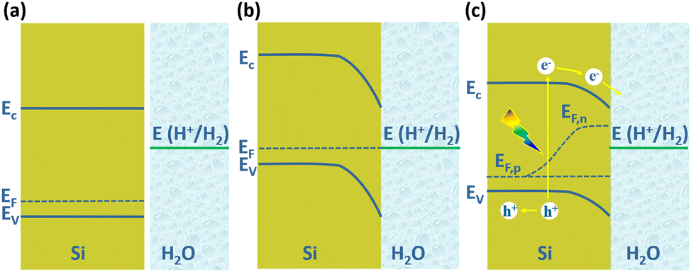
The PEC water splitting reaction on the Si photoelectrode surface is associated with the energy band structure of the Si/electrolyte interface, as shown in Fig. 1 for the example of p-Si. The valence band edge energy (Ev) and conduction band edge energy (Ec) levels of Si are −5.2 eV and −4.1 eV, corresponding to electrochemical potentials of 0.7 V and −0.4 V (vs. NHE), respectively.47 In the case of p-Si, the Fermi level (EF) is near the top of the valence band (Fig. 1a). When p-Si is in contact with the electrolyte, since the EF of p-Si is lower than that of the electrolyte, electrons will transfer from the electrolyte to p-Si until the Fermi levels of the two are equal. This process leads to the formation of net electron space-charge regions on the p-Si surface, causing the energy bands on the surface to bend downward (Fig. 1b). For n-Si, the process is just the opposite, with the energy band on the n-Si surface bending upward. Under illumination, electrons in the valence band of p-Si are excited to the conduction band, causing the equilibrium between p-Si and electrolyte to be disrupted. The departure from equilibrium is quantified in terms of the quasi-Fermi level, i.e., electron quasi-Fermi level (EF,n) and hole quasi-Fermi energy level (EF,p) (Fig. 1c). The photogenerated electrons are transferred to the solution driven by the built-in electric field to reduce H+ to produce H2.
 | ||
| Fig. 1 Schematic diagram of Si/electrolyte interface. (a) Before contact, (b) equilibrium reached after contact in the dark, (c) under illumination. | ||
When a beam of photons are incident on a semiconductor, in addition to reflection and transmission, the remaining photons are absorbed by the semiconductor and excite photogenerated carriers (electron–hole pairs). Some of the photogenerated carriers may be lost during transport to the semiconductor's surface as a result of recombination, and the remainder can be collected on the surface of the semiconductor and transferred to the external circuit or to the solution. Fig. 2 depicts the collection of photogenerated carriers within p-Si near the p-Si/electrolyte interface.48 The light penetration depth (given by 1/α, where α is the absorption coefficient) in a semiconductor is related to the wavelength of the incident light and the band structure of the semiconductor. The light penetration depth of direct bandgap semiconductors is relatively shallow, while that of indirect bandgap semiconductors is relatively deep. For the semiconductor Si with an indirect bandgap, visible light penetrates within it to a depth of 100 μm.49 The diffusion length of the minority carrier (Ln) refers to the average length that the photogenerated hole travels from its creation to recombination with the electron. The Ln is related to the lattice defects and doping of the semiconductor. The more lattice defects and the higher the concentration of impurities, the higher the chance of recombination of photogenerated carriers, the shorter the lifetime and the shorter the diffusion length. The width of the space charge region (or the depletion layer) (W) depends on the type and density of dopants in Si and the potential bias.
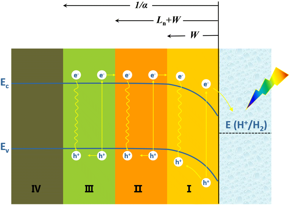 | ||
| Fig. 2 Schematic diagram of the carrier transportation process at the p-Si/electrolyte interface. | ||
In the space-charge region (region I), photogenerated electrons and holes are spatially separated by the built-in electric field and transported by drift. Although some photogenerated carriers recombine, the collection efficiency of photogenerated carriers in this region is high. In region II, photogenerated carrier migration mainly relies on diffusion due to concentration differences. A part of the photogenerated carriers will recombine, and the remaining part can diffuse to the space charge region (region I), where the collection efficiency of photogenerated carriers is also relatively high. In region III beyond the Ln + W, most of the photogenerated minority carrier electrons will be recombined with holes and lost during transport to the semiconductor surface, and the collection efficiency of photogenerated carriers in this region is very low. Ln + W determines the effective collection length of photogenerated carriers. In region IV, the arriving light intensity is very weak, and very few photogenerated carriers are produced.
Another critical step in photogenerated carrier collection is the transfer of photogenerated carriers that reach the surface of the semiconductor to the solution. In addition to the type and concentration of redox pairs in solution and the ambient temperature, the surface states of the semiconductor can have an essential effect on photogenerated carrier collection here, the defect states of the semiconductor surface act as recombination centres for the photogenerated carriers. Even if the photogenerated carriers reach the semiconductor surface, some may recombine at the surface. In addition, regarding electrochemical reaction kinetics, the charge transfer from the electrode to the solution needs to overcome a certain energy potential barrier and requires an overpotential. The electrocatalytic activity of the semiconductor surface directly affects the magnitude of the overpotential required for charge transfer at the semiconductor/electrolyte interface.
Preparation of 1D Si nanostructures
Due to the unique physical and chemical properties of Si, 1D Si nanostructures have been extensively studied and a variety of preparation methods have been developed. For solar hydrogen production applications, ordered arrays of 1D Si nanostructures can be easily and directly fabricated into photoelectrodes and fully utilize the merits of 1D nanostructures. Therefore, we focus here on ordered 1D silicon nanostructure arrays and briefly review some typical preparation methods.Metal-assisted chemical etching
Metal-assisted chemical etching (MACE) has been widely used to prepare 1D Si nanostructure arrays due to its simplicity, low cost, and ease of scale-up preparation. Based on previous studies, Peng et al. developed a method for the preparation of Si nanowire arrays by MACE. The preparation of Si nanowires by MACE is using single-crystal Si wafer as the raw material. First, metal (Ag, Au, Pt, Cu, etc.) nanoparticles or thin films are deposited on the Si wafer by chemical or physical methods; then, Si is etched in an oxidizing HF solution containing oxidizing agents (nitric acid and nitrate, H2O2, etc.) with the metal as a catalyst.50,51 The metal catalyst allows the etching of Si to proceed in a specific direction to form straight holes. When the adjacent holes penetrate each other, the remaining hole walls take on a 1D structural morphology. Ag nanoparticles are the most commonly used catalyst for the preparation of 1D Si nanostructures by the MACE method. Based on the experimental observations, Peng et al. proposed an electrokinetic model to explain the microscopic dynamic origin of motility of Ag nanoparticles in Si during the chemical etching process, as shown in Fig. 3a.52 The energy generated in the in situ bipolar electrochemical reaction on the surface of the Ag nanoparticles can be directly converted into mechanical work, which drives the movement of the Ag nanoparticles in Si with the help of HF.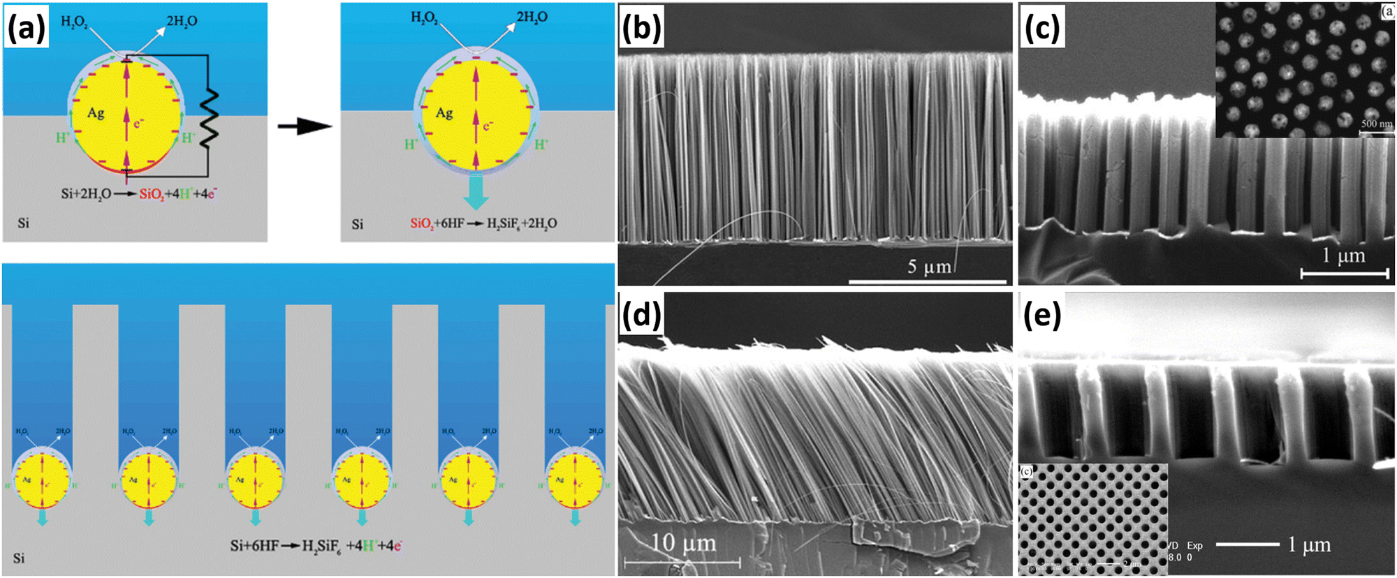 | ||
| Fig. 3 (a) Catalytic-induced electrokinetics for autonomous Ag particle movement in bulk Si. SEM images of 1D Si nanostructures prepared by MACE. (b) Perpendicular Si nanowire arrays. (c) Highly order Si nanowire arrays, (d) slanted Si nanowire arrays, reproduced with permission from ref. 52, Copyright © 2008 Wiley-VCH Verlag GmbH & Co. KGaA, Weinheim. and (e) highly ordered Si nanohole arrays. (a and d) Reproduced with permission from ref. 52, Copyright © 2008 Wiley-VCH Verlag GmbH & Co. KGaA, Weinheim. (b) Reproduced with permission from ref. 51, Copyright © 2013 Wiley-VCH Verlag GmbH & Co. KGaA, Weinheim. (c) Reproduced with permission from ref. 53, © 2007 American Institute of Physics. (e) Reproduced with permission from ref. 56, Copyright © 2010, American Chemical Society. | ||
A very simple method to prepare metal catalysts is to reduce metal ions in solution into metal nanoparticles using the reducing Si–H bonds on the surface of HF-treated Si wafer. Subsequently, the ordered Si nanowire arrays can be obtained by MACE with the catalytic effect of metal catalysts. The benefits of the Si–H bond reduction method for the preparation of metal catalysts are simplicity, low cost and short time consumption, but the method cannot precisely control the morphology of the metal catalysts, resulting in the low controllability of the prepared Si nanowires (Fig. 3b). Therefore, Peng et al. proposed a method to prepare regular Ag nanoholes on Si sheets by physical vapor deposition using silica nanosphere as a template for lithography.53 The Si nanowire arrays prepared with such Ag nanopholes as catalysts were highly ordered, as shown in Fig. 3c. Using this method, the diameter, spacing, and alignment of Si nanowires can be easily and precisely tuned by the adjustment of the lithography pattern. In addition to Si nanowires perpendicular to the substrate, tilted Si nanowires,52 zigzag Si nanowires,54,55 Si nanoholes,56etc. have also been prepared by changing the MACE process conditions.
Chemical vapor deposition
Chemical vapor deposition (CVD) is the condensation of one or more compounds from the gas phase onto a substrate where a reaction occurs to produce a solid deposit.57 In the CVD process, the deposition of solids can follow different mechanisms to form different morphologies. Among them, vapour–liquid–solid (VLS) is a mechanism widely used to prepare 1D nanostructures. 1D Si nanostructures can be synthesized “bottom-up” by employing metal nanoclusters as catalysts via a VLS mechanism.58,59Fig. 4a illustrates the growth mechanism of a Si nanowire with Au as the catalyst.60 At high temperature, Si atoms decomposed from the Si precursor (SiH4, SiCl4, etc.) form eutectic droplets together with Au catalyst. As the reaction proceeds, Si is continuously dissolved by the Au–Si eutectic droplets in increasingly high concentrations, leading to supersaturation and precipitation of crystals. The solid–liquid interface forms the growth interface, which acts as a sink for Si to continue to incorporate into the lattice, thus allowing the Si nanowires to grow in the presence of Au–Si alloy droplets. The diameter of the Si nanowire is determined by the size of the catalyst droplet. The nanowire growth process catalyzed by Au nanoclusters based on the VLS mechanism was observed by in situ TEM.61 To prepare highly ordered arrays of 1D Si nanostructures, lithography patterning technique was utilized to prepared ordered catalyst arrays for the VLS process.62Fig. 4 b,c show a virtually defect-free Si wire array exhibiting extremely narrow diameter and length distributions, as well as highly controlled wire placement. Highly ordered Si nanowire arrays have also been prepared by VLS growth of Si nanowires within nanopores of the anodic aluminum oxide (AAO) template.63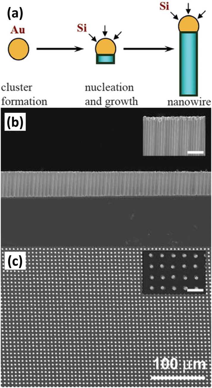 | ||
| Fig. 4 (a) Schematic diagram of VLS growth of Si nanowires. Reproduced with permission from ref. 60, © 2006 IOP Publishing Ltd Side-view (b) and top-view (c) SEM images of a Au-catalyzed Si wire array. Reproduced with permission from ref. 62, © 2007 American Institute of Physics. | ||
In addition to the VLS mechanism, several other mechanisms have been developed for the preparation of 1D Si nanostructures, such as oxide-assisted growth (OAG) mechanism,64 solution–liquid–solid (SLS) mechanism,65etc.
Other methods
MACE and CVD are the most commonly used methods for the preparation of 1D Si nanostructures that are used as photoelectrodes for solar hydrogen production. In addition to these, several other preparation methods have been explored. For example, using ordered arrays of gold particles produced by nanosphere lithography as catalysts, ordered arrays of vertically aligned Si nanowires were fabricated by molecular beam epitaxy (MBE) method.66 Close-packed arrays of Si nanopillars over an entire 4 in. wafer were prepared by the synergy of Langmuir–Blodgett (LB) assembly and reactive ion etching (RIE).67 SiO2 particles with diameters ranging from 50 to 800 nm were assembled on the Si wafer by LB method. Si nanopillars were formed by Cl2 based selective and anisotropic RIE of the Si substrate. Further, sharp Si nanocones could be prepared by the undercutting through control of the etching conditions, as shown in Fig. 5. Compared with MACE, RIE has better morphological controllability, but it requires more expensive equipment and a complex process, which substantially increases the cost of preparing 1D Si nanostructures.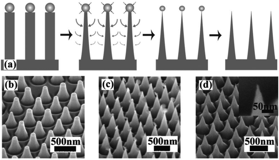 | ||
| Fig. 5 (a) Schematic of sharpening process. (b)–(d) SEM images show the morphologies of each step. Reproduced with permission from ref. 67, © 2008 American Institute of Physics. | ||
Advantages of 1D Si nanostructures
For solar hydrogen production applications, the 1D Si nanostructures provide several potential advantages over the traditional planar Si photoelectrode.36,68Large surface area
When a semiconductor photoelectrode is immersed in an electrolyte, the electrochemically active species in the solution diffuse to the electrode surface and exchange electrons with the electrode to be oxidized or reduced. The larger the specific surface area of the electrode, the larger the electrochemical reaction site and the more opportunities for the electrochemically active species to contact the electrode surface and react. Therefore, increasing the specific surface area of the photoelectrode is beneficial for increasing the photocurrent density and reducing the overpotential required to achieve the desired current. 1D Si nanostructured photoelectrodes have a much larger specific surface area than planar Si photoelectrodes. For example, the surface area of a photoelectrode with an area of 1 μm × 1 μm is 1 × 10⁻¹² m2. When nanowires with a diameter of 100 nm and a length of 10 μm are grown on the surface of the electrode, and the distance between each nanowire is 100 nm, the surface area of the photoelectrode is 7.95 × 10⁻¹¹ m2, which is about 80 times that of the planar electrode. In addition, the large specific surface area provides more sites that can be used to load catalysts, reducing the high activity requirement for individual sites by increasing the loading of catalysts per unit area, thus allowing the replacement of noble metal catalysts with inexpensive transition metal catalysts that have relatively poor catalytic activity.69Enhanced light absorption
Planar Si photoelectrodes have a strong reflective effect on light, resulting in a large portion of the light being lost. The nanostructured photoelectrode overcomes this drawback and dramatically improves the light absorption of the photoelectrode through the antireflection effect.34 Especially, 1D nanostructured arrays of Si can generate significant “light trapping” effects, resulting in better antireflection effects and better light absorption.70 Peng et al. investigated the light reflection properties of single-side polished Si wafers with Si nanowire arrays on the surface.71,72 It was found that the reflectance of Si wafers was as high as 17–40% in the 300–1000 nm range, while the reflectance of Si nanowire arrays was only 2.1% or less. The morphology of the 1D Si nanostructures will affect their anti-reflectivity. The optical absorption properties of thin film and 1D nanostructures (nanowires and nanocones) of a-Si:H are shown in Fig. 6.73 Photographs of the three samples are quite different. The Si thin film is mirror-like and highly reflective. The Si nanowires reflect less light while the Si nanocones look black, exhibiting enhanced absorption due to suppression of reflection from the front surface. The measured and calculated absorption spectra of the three samples over the wavelength range of 400–800 nm quantitatively demonstrate the visible absorbance of the three samples. 1D Si nanostructures have a significantly enhanced light absorption capacity. In particular, the Si nanocones maintain an absorption rate of more than 93% between 400 and 650 nm.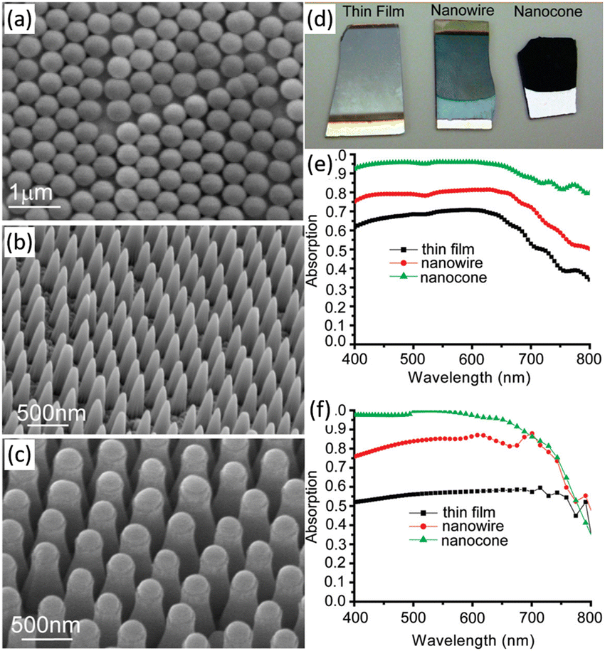 | ||
| Fig. 6 SEM images (a–c), photograph (d) and the measured (e) and calculated (f) absorption spectra of Si thin film, nanowires and nanocones. Reproduced with permission from ref. 73, Copyright © 2009, American Chemical Society. | ||
The Si nanowire arrays prepared by MACE have excellent anti-reflection effect.74–76 However, the MACE process is carried out in an aqueous solution, and the surface tension of water causes the Si nanowires to agglomerate into bundles during the drying process, which may reduce the antireflection effect. It was found that post-treatment of Si nanowire arrays prepared by MACE in KOH solution was able to separate Si nanowires from bundles by sharpening the top-ends of the nanowires.77 As shown in Fig. 7a and b, the light reflectivity of Si nanowire arrays in the 300–1000 nm range was dramatically reduced after tapered Si nanowires formed by KOH treatment. The Si nanowires treated with 60 s in KOH showed the best antireflection performance with an average reflectance of less than 1%. This increase in reflectivity by changing the geometry of the Si nanowires is attributed to the multiple scattering and graded refractive index (GRI) effects, as shown in Fig. 7c–f.
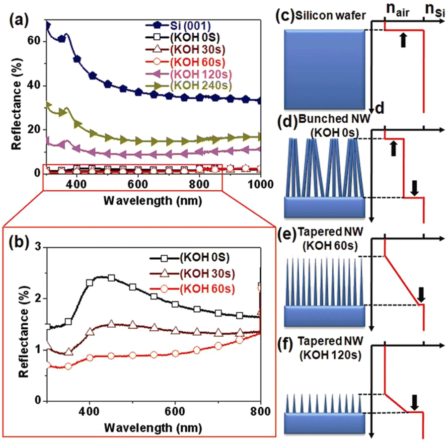 | ||
| Fig. 7 (a and b) Optical reflective spectra recorded from different samples. (c–f) Schematic representation of the correlation between Si nanowire morphology and effective refractive index profile. Reproduced with permission from ref. 77, Copyright © 2011, The Optical Society. | ||
Decoupled light absorption and charge-carrier collection
For PEC hydrogen production, the semiconductor absorbs light to produce electron–hole pairs. The electrons or holes need to be transported to the surface of the semiconductor to react with the electrochemically active material in the solution. As mentioned earlier, the indirect bandgap semiconductor Si has a light penetration depth of up to 100 μm. For conventional planar Si photoelectrodes, some photogenerated carriers need to travel distances of up to several tens of microns to reach the surface where the reaction takes place. In this process, many carriers will be recombined, resulting in low carrier utilization (Fig. 8a). The construction of photoelectrodes with 1D Si nanostructures is an excellent solution to this problem. As shown in Fig. 8b, after the 1D Si nanostructure is excited by light to generate photogenerated carriers, the minority carriers can be quickly transported to the surface for HER or OER reactions through the radial direction of the 1D nanostructure, which is in the nanometer scale in two dimensions. The short distance of this process dramatically degrades the chance of carrier recombination and improves carrier utilization. At the same time, the 1D Si nanostructure is continuous in one dimension, providing high-speed channels for the transport of the majority carriers to the substrate. This feature allows the use of low-purity Si with a short minority carrier diffusion length, significantly reducing the manufacturing cost of photoelectrodes.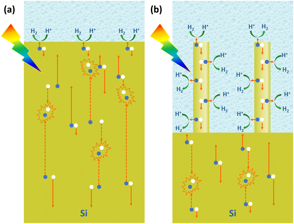 | ||
| Fig. 8 Schematic diagram of the photogenerated carrier separation and transportation in the planar Si photoelectrode (a) and 1D Si nanostructured photoelectrode (b). The blue balls and white balls represent photogenerated electrons and photogenerated holes, respectively. | ||
Based on the advantages of 1D Si nanostructures, their superiority as photoelectrodes for PEC water splitting has been extensively reported. It is well established that 1D Si nanostructured photoelectrodes exhibit lower overpotential and higher photocurrent than planar Si photoelectrodes.78–80 Oh et al. investigated the PEC hydrogen production performance of Si nanowire arrays fabricated by MACE.81 As shown in Fig. 9a, the HER photocurrent for planar Si is very small until the potential reaches −0.5 V. In contrast, the Si nanowire photocathode produces a much higher photocurrent, with an onset potential of 0.2 V, which is more positive than the planar Si. This positive onset potential comes from the higher photovoltage of the Si nanowire photoelectrodes, as shown in Fig. 9b for the cyclic voltammetry test results of methylviologen. The increase in the photovoltage of the Si nanowire photocathode is attributed to the reduction of the overpotential, the favorable shift of the flat-band potential, and the light trapping or antireflection effect of the nanowires.
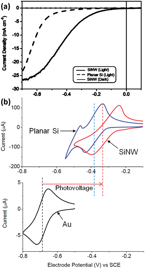 | ||
| Fig. 9 (a) PEC HER performance comparison of the Si nanowire and planar Si. (b) Cyclic voltammetry curves of methylviologen on the Si nanowire and planar Si photoelectrode under illumination and on the Au electrode in the dark. Reproduced with permission from ref. 81, Copyright © 2012, American Chemical Society. | ||
Modification with co-catalysts
The kinetics of both HER and OER are sluggish on the bare Si surface, resulting in a large overpotential for water splitting. The most effective solution to this problem is to load a co-catalyst with high catalytic activity on the surface of Si. Then the next question is which material to choose as a co-catalyst. Purely from the point of view of reducing the overpotential, the catalytic activity of the co-catalyst is desired to be as high as possible. A direct criterion for the kinetic rate of a particular reaction at an electrode is the exchange current density (j0). When an electrode reaction is in equilibrium, the reaction rate in the anodic direction is equal to the reaction rate in the cathodic direction. The values of the anode-direction current (Ia) and the cathode-direction current (Ic) are equal, i.e., Ia = Ic = I0. The current density I0/A (A is the electrode area) = j0, i.e., the exchange current density.82 The value of j0, which can be calculated from the Tafel curve, directly reflects the speed of the electrode reaction. The larger j0 is, the faster the reaction rate is. The j0 of HER on Si is very low (≈10−8 A cm−2), indicating the sluggish HER kinetics on Si. In addition to the evaluation factor j0, which can only be obtained by measurement, catalytic activity descriptors based on DFT calculations have been proposed to predict the catalyst activity and guide catalyst design. For HER, the free energy change of H adsorption on the catalyst surface (ΔGH) is the descriptor of the catalytic activity of a catalyst.83 The HER occurring on the electrode surface undergoes a two-step process as follows:| Step 1: H+ + e− + * → H* (Volmer step) |
| Step 2: H* + H+ + e− → H2 + * (Heyrovsky step) |
| 2H* → H2 + 2* (Tafel step) |
Noble metals
In the volcano diagram, precious metals such as Pt are located at the top of the volcano in favor of HER. Among them, Pt with ΔGH close to 0 eV and the j0 up to 10−3 A cm−2 is recognized to be the catalyst with the highest HER catalytic activity available.83 Therefore, Pt is an ideal co-catalyst for achieving high-performance HER on 1D Si nanostructures.81,84,85 Wang et al. prepared Si nanowire arrays using MACE and loaded Pt nanoparticles on Si nanowires.86 Electroless deposition (ELD) and atomic layer deposition (ALD) were utilized to synthesize Pt nanoparticles on Si nanowires. As shown in Fig. 10, the PEC HER of the Si nanowire photocathode was significantly improved after loading Pt nanoparticles. The Pt/Si nanowire photocathode prepared by the ALD method performed best. This may benefit from the uniform attachment of small-sized Pt nanoparticles on the Si surface and the effective charge transfer ensured by single-crystal Pt nanoparticles with single-crystal Si. It was also reported that the Pt electrocatalysts prepared by electron-beam evaporation showed much higher catalytic activity for HER than that prepared by electroless deposition.69 The electroless Pt films produced a linear J–E electrocatalytic response, indicating a resistive behavior. In contrast, the e-beam deposited Pt films showed the expected exponential response. However, the e-beam-evaporated Pt films formed ohmic contact with p-Si, resulting in no photovoltage.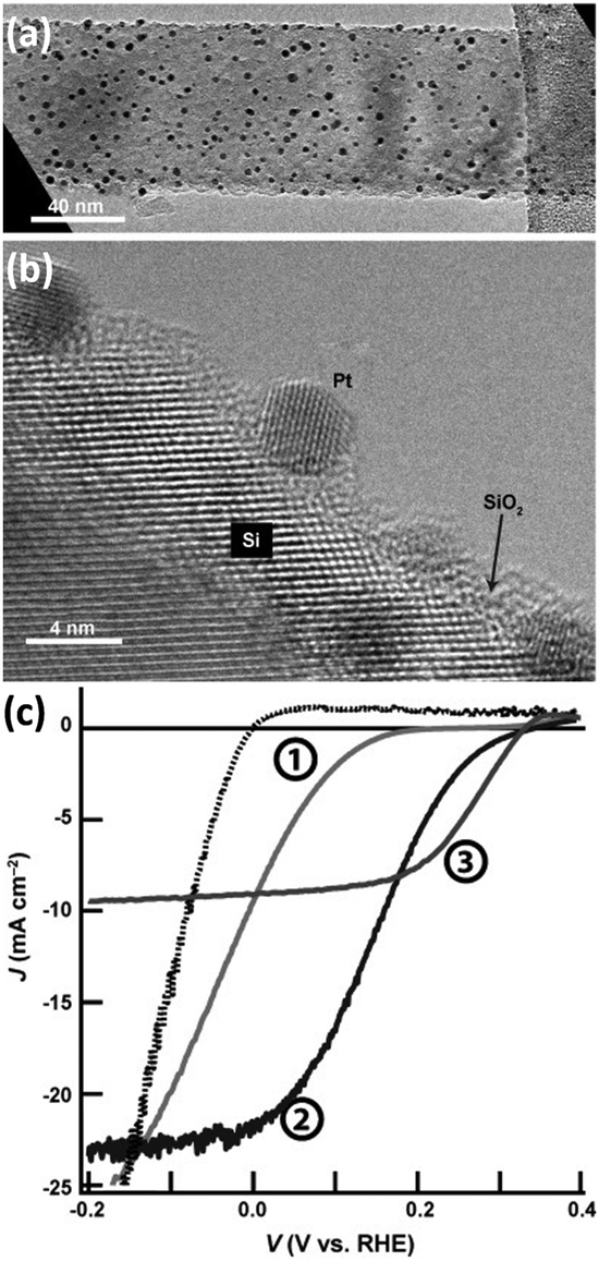 | ||
| Fig. 10 (a) TEM and (b) HRTEM images of Pt nanoparticles modified Si nanowire, (c) PEC HER performance of naked Si nanowires (①), and Si nanowires modified with Pt nanoparticles prepared by ELD (②) and ALD (③). Reproduced with permission from ref. 86, Copyright © 2013 Wiley-VCH Verlag GmbH & Co. KGaA, Weinheim. | ||
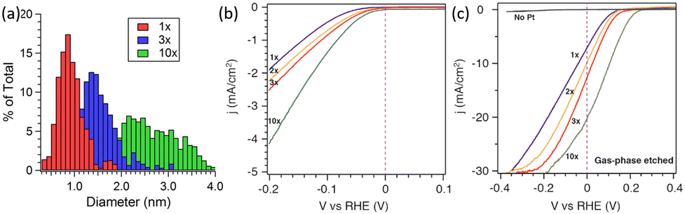
In addition to the preparation method, the catalytic activity of Pt nanoparticle-modified 1D Si nanostructures was greatly affected by the Pt loading. Yang et al. investigated the effect of ALD cycles on the PEC performance of Pt/Si nanowires.87 As shown in Fig. 11a, the average diameter of Pt nanoparticles is approximately 0.8 nm after one ALD cycle. As the number of cycles increases, the particle size increases, and the size distribution is broader. Fig. 11b shows that the electrochemical performance also improves with the increase in ALD cycles, which may benefit from the increase in Pt loading. Photoelectrochemical tests showed that blank Si had almost no catalytic activity (Fig. 11c). After loading Pt nanoparticles, the PEC performance of the photoelectrode was greatly improved. As the number of cycles increased from 1 to 10, the photocurrent density at 0 V vs. RHE increased from 7 to 21 mA cm−2, and the slope of the j–v curve increased, indicating that the HER catalytic activity increased.
 | ||
| Fig. 11 (a) Histogram of Pt particle size for various numbers of ALD cycles, (b) electrochemical and (c) photoelectrochemical performance of Pt cocatalysts loaded via ALD in 0.5 M H2SO4 electrolyte. Reproduced with permission from ref. 87, Copyright © 2013, American Chemical Society. | ||
Other platinum group metals such as Ru and Ir have also been used as HER co-catalysts for Si nanowire photoelectrodes.88,89 Shao et al. prepared Ru nanoparticles modified Si nanowire photoelectrode by reducing Ru ions by Si–H bonds.88 The optimized Ru/Si nanowires exhibited low overpotential, good stability and low theoretical activation energy for HER. Ir–Au bimetal nanoparticles were also used as highly active catalyst to modify Si nanowires.89 Besides, Ag was found to be a good cocatalyst for modifying 1D Si nanostructures to improve the HER kinetics.90,91
Non-noble metals
In addition to catalytic activity, the cost of the catalyst should also be considered when selecting a co-catalyst. Due to the scarcity and high price of noble metals, there is a desire to replace them with non-noble metal catalysts. Metal Ni and its alloys are the most studied co-catalysts for modifying 1D Si nanostructured photoelectrodes thanks to their low price and relatively high catalytic activity. The performance of Ni and Ni–Mo as co-catalysts for the modification of 1D Si nanostructured photoelectrodes was evaluated and compared with Pt.69 It was found that the catalytic activity for HER increased in the following order: Ni < Ni–Mo ≤ Pt, as shown in Fig. 12a. The electrocatalytic activity of Ni–Mo deposited for 180 s was even better than that of the electroless deposited Pt. However, the open circuit potential (Voc) and short circuit photocurrent densities for the photocathodes followed by the order Ni–Mo < Ni < Pt (Fig. 12b) due to the “pinch-off” effect.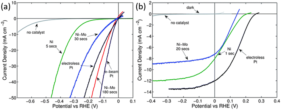 | ||
| Fig. 12 (a) Polarization data of the HER activities of various catalysts on p+-Si microwire electrodes, (b) polarization data of the HER activities of various catalysts on illuminated p-Si microwire array photoelectrodes. Reproduced with permission from ref. 69, Copyright © The Royal Society of Chemistry 2011. | ||
To improve the performance of the Ni–Mo co-catalyst-modified Si photocathode, Lewis et al. prepared Si microwire arrays with buried radial n+p junction.92 The Ni–Mo-coated n+p-Si microwire photoelectrode yielded a Voc as high as 0.46 V. Further, a light-scattering layer of TiO2 nanoparticles were introduced to this system to eliminate the light blocking by the Ni–Mo catalyst layer (Fig. 13a and b).93 The TiO2 layer scattered light back into the Si microwire array, while optically obscuring the underlying Ni–Mo catalyst film. In turn, the mass loading of Ni–Mo films is sufficient to produce high catalytic activity for HER on a geometric area basis. The best-performing Ni–Mo/TiO2/n+p-Si microwire array photoelectrode yielded a photovoltage of 420 mV. Fig. 13c shows that the external quantum efficiency (EQE) of Ni–Mo/TiO2/n+p-Si microwire array photoelectrode is close to that of Pt/TiO2/n+p-Si microwire array photoelectrode.
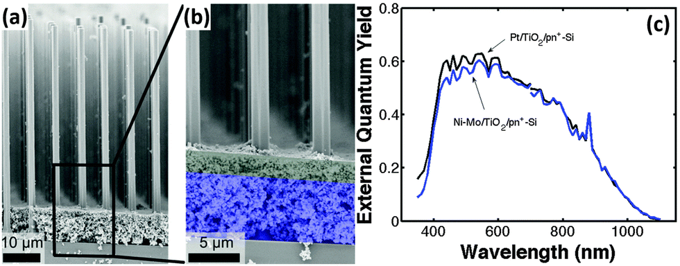 | ||
| Fig. 13 (a and b) SEM images of the Ni–Mo/TiO2/n+p-Si microwire array, (c) spectral response data for the best-performing n+p-Si microwire-array photocathode loaded with Ni–Mo and TiO2 scattering particles (blue curve) and for the best-performing n+p-Si microwire-array photocathode loaded with Pt and TiO2 scattering particles (black curve). Reproduced with permission from ref. 93, Copyright © The Royal Society of Chemistry 2015. | ||
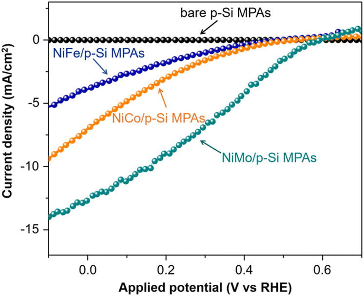
Tung et al. investigated the PEC HER performance of p-Si micropillar array photoelectrodes electrodeposited with Ni–M (M = Co, Fe, Mo) alloys as catalysts.94 As shown in Fig. 14, the performance of p-Si micropillar array photoelectrodes modified with Ni–M co-catalyst showed the following trend Fe < Co < Mo. The in situ and ex situ tracking characterizations (XPS/XAS, GAXRD) revealed that the in situ formed surface Ni2+ species during solar-driven hydrogen evolution is the primary factor for yielding the active site in Ni–M/p-Si micropillar arrays photocathodes. The presence of high-valence Mo species (Mo4+ and Mo6+) could stabilize the high valence of Ni2+ species near the catalyst surface, leading to the high catalytic activity of Ni–Mo.
 | ||
| Fig. 14 PEC HER performance of p-Si micropillar arrays modified with Ni–Fe, Ni–Co and Ni–Mo as cocatalysts. Reproduced with permission from ref. 94, Copyright © 2020 Wiley-VCH Verlag GmbH & Co. KGaA, Weinheim. | ||
In order to achieve the high catalytic activity, Ni–Mo catalysts with high loading on the Si surface are required. Since Ni–Mo is impermeable to light, the resulting parasitic light absorption will affect the photoelectrode performance. To solve this problem, Vijselaar et al. designed and fabricated a Si microwire array photoelectrode by varying the fraction of Ni–Mo catalyst coverage over the microwires.95 Three types of photoelectrodes were designed: completely exposed microwires (a), microwires passivated by SiO2 with exposed tops (b), and microwires with a defined exposed area in the range of 2–36 μm from the top (c). Ni–Mo nanoparticles were electrodeposited on the exposed area of the microwires. The photoelectrical measurements indicated that the loading of Ni–Mo significantly decreases photocurrent densities due to blocking and/or scattering the light. In contrast, the photoelectrochemical HER test results show that photocurrent and photovoltage substantially increased after loading the Ni–Mo catalyst. For the c-type samples, the PEC HER performance was optimized by adjusting the distance between Si microwires and the spatioselective coverage of Ni–Mo on the microwires, resulting in a photovoltage of up to 495 mV.
Si is easily oxidized to form Si oxide on the surface, which will hinder charge transfer. Therefore, the direct use of 1D Si nanostructures as photoanodes for water oxidation is rarely investigated because of the great difficulties. Tung et al. demonstrated the decoration of isolated Ni nanoparticles as both protecting layer and OER electrocatalysts on the surfaces of n-Si microwires.96 The stability of the photoelectrode was determined by the loading of the Ni catalyst. If the loading is too small, the stability is poor; and if the loading is too large, the light absorption is affected. The optimized Ni/n-Si microwire arrays photoelectrode showed an OER onset potential of 1.08 V vs. RHE and a saturation photocurrent of 35.5 mA cm−2.
MoSx
The DFT-calculated ΔGH of the MoS2 is slightly positive at +0.08 eV, suggesting that it might be a suitable catalyst for HER.97,98 Tran et al. deposited MoS2 co-catalyst on Si nanowires by photo-assisted electrodeposition, as shown in Fig. 15a and b.99 The layer structured MoS2 was assembled tightly on the surface of Si nanowires. The HER onset potential of MoS2/Si nanowire photoelectrode under illumination is 0.25 V vs. RHE, which is about 200 mV more positively shifted than that of Si nanowires without loading of MoS2 co-catalyst (Fig. 15c). As shown in Fig. 15d, the MoS2/Si nanowire photoelectrode exhibited comparable PEC performance to the Si nanowire photoelectrode modified with Pt nanoparticles, indicating the great potential of MoS2 as a candidate for Pt. Similar results were obtained on the thermolysis-prepared MoS2/Si photoelectrode.100 MoS2 acted not only as a catalyst but also as a light absorber to improve the PEC activity of the Si nanowire photoelectrode.101 The MoS2/Si Schottky junction enhances the photo-generation of electron–hole pairs and suppresses carrier recombination. The low charge-transfer resistances at the semiconductor/catalyst and catalyst/electrolyte interfaces, slow carrier recombination dynamics, and consequently efficient charge carrier separation resulted in superior performance.102 Zinc 1T-phase MoS2 synthesized by the hydrothermal method was drop cast onto Si nanowires.103 While improving the catalytic activity of the photoelectrode, MoS2 also prevents the growth rate of the natural oxide layer SiOx on the Si surface, significantly improving the stability of the photoelectrode. In addition, a Ag interface layer was introduced between Si nanowire and MoS2 to improve carrier utilization.104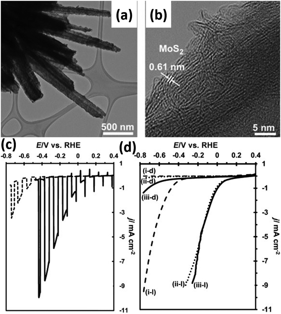 | ||
| Fig. 15 TEM (a) and HRTEM (b) images of the MoS2/Si nanowires. Comparation of the photoelectrochemical HER performance: (c) Si nanowires and MoS2/Si nanowires, (d) Si nanowires modified with MoS2 or Pt nanoparticles in the dark or under illumination. Reproduced with permission from ref. 99, Copyright © 2012 Wiley-VCH Verlag GmbH & Co. KGaA, Weinheim. | ||
The multiple valence states of Mo lead to the presence of a wide range of molybdenum sulfides. In addition to MoS2, other molybdenum sulfides have been used as co-catalysts for 1D Si nanostructure photoelectrodes and have shown excellent performance.105–108 Hou et al. modified 1D Si pillars with bioinspired incomplete cubane-like Mo3S4 clusters to evolve hydrogen at a rate comparable to that of Pt.109 After modified with Mo3S4 clusters, the onset potential of the photoelectrode shifted from −0.4 V vs. RHE to 0.15 V vs. RHE. That is, the Mo3S4 co-catalyst reduces the HER overpotential of the p-Si photoelectrode by 550 mV. Further, 1D Si pillars with a diameter of 3 μm and a length of 50 μm were prepared by photolithography to improve the performance of the p-Si photoelectrodes. Compared with planar photoelectrodes, p-Si photoelectrodes with pillar structure showed great superiority in onset potential, saturation current density, and incident photon-to-current conversion efficiency (IPCE). The limiting current density and IPCE of the photoelectrode are reduced after loading the co-catalyst, which can be due to the co-catalyst hindering the light absorption of the photoelectrode. Therefore, the balance between catalytic activity and light absorption performance should be considered when designing and constructing the photoelectrodes. Too little catalyst will not achieve a sufficient catalytic effect, while too much catalyst will affect light absorption.
Metal compounds
Inspired by the excellent HER catalytic activity of MoS2, other metal sulfides have also been investigated as co-catalysts for 1D Si nanostructured photoelectrodes. P-Si nanowires were modified with tungsten sulfides (crystalline WS2 and amorphous WS3) prepared by pyrolysis.110 Compared with the crystalline WS2, the amorphous WS3 had larger surface area and more active sites, resulting in higher catalytic activity in HER. CoS2 was used as a co-catalyst to enhance the HER catalytic activity of Si microwire photoelectrodes while protecting Si from oxidation and reductive degradation.111 It was suggested that more vacancies in the S-3p unoccupied states of the CoS2–Si electrode were presented with a lower negative charge of S22− to form weaker S–H bond strength, promoting water splitting efficiency. 2D layered VS2 synthesized by CVD was wrapped on the surface of Si nanowires for highly efficient PEC water reduction.112CoP has been reported to be one of the most active, acid-stable, earth-abundant HER electrocatalysts.113,114 Therefore, it was utilized as a co-catalyst for 1D Si nanostructure photoelectrodes.115–117 Hollow Co2P spheres were prepared on the Si nanowire surface by photo-assisted electrodeposition and phosphorization. This resulted in a remarkably positively shifted onset potential for PEC HER.115 Conformal and continuous Co2P was coated on the highly ordered Si nanowire arrays by drop-casting method followed by low-temperature phosphorization.116 The Co2P layer improved the HER catalytic activity of the photoelectrode while protecting the Si from photo-oxidation and improving the lifetime of the photoelectrode. FeP was also an efficient HER co-catalyst for the 1D Si nanostructured photoelectrodes.118 Tetragonal phase Ni12P5 nanoparticles was utilized as an efficient co-catalyst to modify p-Si nanowire arrays, an optimal overpotential of 143 mV was required for 20 mA cm−2 current density.119
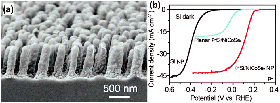
Uniform amorphous NiCoSex shells were photo-assisted electrodeposited on the bamboo shoot-like Si nanopillars to fabricate the p-Si/NiCoSex core/shell nanopillar array photoelectrode (Fig. 16a).120 The good optical transparency and the excellent electrocatalytic activity boosted the generation and utilization of the photogenerated electrons. As shown in Fig. 16b, the onset potential (J = −0.1 mA cm−2) of the p-Si/NiCoSex core/shell nanopillar array photoelectrode is about 0.25 V vs. RHE, which is much more positive than that of the p-Si nanopillar photoelectrode. It is worth noting that the performance of the planar photoelectrodes in terms of onset potential and photocurrent is much worse compared to the 1D nanostructured photoelectrodes. The phase structure of a catalyst predominantly affects its catalytic activity. Three possible polymorphs of nickel selenide (orthorhombic phase NiSe2, cubic phase NiSe2, and hexagonal phase NiSe) were investigated as bifunctional electrocatalysts for both PEC water reduction and oxidation on 1D Si nanowire arrays.121 It was found that the orthorhombic NiSe2 nanocrystals exhibited the best PEC water splitting performance, owing to the more metallic nature and the formation of fewer surface oxides.
 | ||
| Fig. 16 (a) SEM image of the p-Si/NiCoSex core/shell nanopillar array, (b) PEC HER performance. Reproduced with permission from ref. 120, Copyright © The Royal Society of Chemistry 2016. | ||
In addition to the metal sulfides, metal phosphides, and metal selenides mentioned above, metal oxides,122–125 metal borides,126 and metal carbides,127 and other metal compounds128,129 have also been used as HER or OER co-catalysts for 1D Si nanostructured photoelectrodes.
Carbon materials
Although metals and metal compounds have achieved remarkable success in enhancing the performance of 1D Si nanostructured photoelectrodes as co-catalysts, the high cost (mainly referring to precious metals), light scattering, and stability issues have prompted the development of non-metallic catalysts. Sim et al. first demonstrated that N-doped graphene as a co-catalyst can significantly enhance the PEC HER performance of p-Si photocathodes.130 Then they applied the idea to 1D Si nanowire array photoelectrodes.131 As shown in Fig. 17a, the N-doped graphene quantum sheets (N-GQS) were obtained by replacing some C atoms with N atoms through N2-plasma treatment. The N-GQS were modified on the surfaces of 1D Si nanowires by drop-casting. Photoelectrochemical and electrochemical tests showed that N-GQS has excellent HER catalytic activity (Fig. 17b). For the planar Si electrode, the PEC HER onset potential was positively shifted by 0.3 mV after modification with N-GQS. However, the difference is minimal for Si nanowire photoelectrodes, only 0.09 V. Due to the excellent light transmission of N-GQS, the photocurrent of the photoelectrode did not decrease significantly after loading the co-catalyst. Yu et al. fabricated reduced graphene oxide (rGO)-decorated Si nanowire array photocathode by a flexible and scalable electrochemical reduction method.132 In addition to 2D nanostructured graphene, another characteristic carbon material, 1D nanostructured carbon nanowires, is also used as a co-catalyst for 1D Si nanostructured photoelectrodes. Si nanowire arrays were modified with hierarchically branched carbon nanowires that exhibited outstanding catalytic activity for HER and excellent stability against photo-oxidation and corrosion.133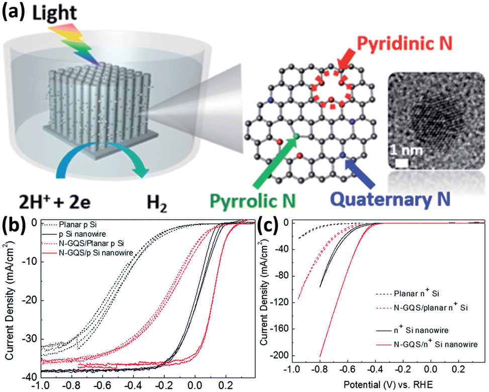 | ||
| Fig. 17 (a) Schematic of N-doped graphene quantum sheets (N-GQSs) decorated on a Si nanowire photocathode electrode. (b) Photoelectrochemical and (c) electrochemical HER performance of the planar and 1D nanostructured Si photoelectrodes with/without N-GQS catalysts. Reproduced with permission from ref. 131, Copyright © The Royal Society of Chemistry 2015. | ||
For co-catalysts used to modify 1D Si nanostructures, the highest catalytic activity is still that of the noble metal Pt. However, considering issues such as cost and abundance, some non-precious metal catalysts are good choices, such as Ni-based alloys, sulfides of Mo, etc. Although the activity of these co-catalysts still is still somewhat inferior to that of Pt, it is expected to be further improved by several means, such as the high entropy alloy catalysts which have emerged in recent years. The strategy of single-atom catalysts, combining small amounts of noble metals with non-precious metals, can also be considered to obtain high performance at relatively low cost.
1D Si nanostructured heterojunction
The loading of co-catalysts with high electrocatalytic activity on the surface of 1D Si nanostructures solves the problem of sluggish reaction kinetics of water splitting on Si surfaces and dramatically reduces the water splitting overpotential. However, the narrow band gap of Si results in a low photovoltage, and its valence band potential is insufficient to oxidize water. These make it necessary to apply a large applied voltage to enable the PEC water splitting reaction. Combining Si with other semiconductors to form heterostructures effectively solve the high overpotential due to energy band structure.Type I heterojunction
Different heterojunctions can be formed between two semiconductors, depending on their conductivity types and energy band structures. A Type I heterojunction is formed between two semiconductors with a straddling bandgap. In this structure, both photogenerated electrons and photogenerated holes are transported from the semiconductor with wider band gap to the semiconductor with narrower band gap. The accumulation of photogenerated carriers within one semiconductor will greatly increase the chance of recombination of photogenerated electrons and holes. From this point of view, the Type I heterojunction is unfavorable for PEC hydrogen production applications. Nevertheless, there have still been some reports of the 1D Si nanostructures-based Type I heterojunctions for solar water splitting applications, including Si nanowires/CdSe quantum dots,134 Si nanowires/g-C3N4 shell arrays,135 Si nanowires/g-C3N4 nanosheets,136 and Si nanowires/SrTiO3 nanoparticle-coupled g-C3N4 nanosheets.137Fig. 18 shows the schematic diagram of the energy band alignment and charge transporting process in the Si/g-C3N4 heterojunction.135 Under illumination, electrons in the valence bands of Si and g-C3N4 jump to the conduction bands and generate holes in the valence bands. The holes are transferred to the surface of the photoelectrode to oxidize water and produce O2. The photogenerated electrons are transferred from the conduction band of g-C3N4 to the conduction band of Si under the effect of the built-in electric field. They are transferred through an external circuit to the counter electrode for HER.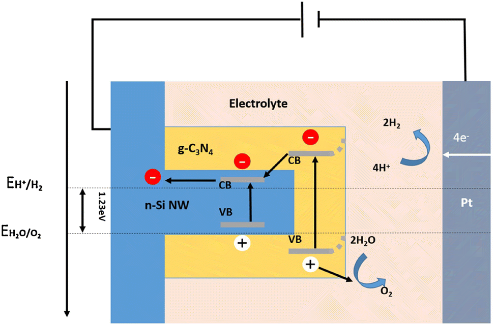 | ||
| Fig. 18 Schematic diagram of energy band alignment of the Si/g-C3N4 heterojunction. Reproduced with permission from ref. 135, Copyright © 2016 Published by Elsevier B.V. | ||
Type II heterojunction
Another structure that is more favourable for the separation of the photogenerated carriers than the Type I heterojunction is the Type II heterojunction. Fig. 19a shows the energy band structure of a Type II heterojunction consisting of a p-type semiconductor (S1) and an n-type semiconductor (S2) with staggered band alignment.138 Since the Fermi level of S2 is higher than S1; electrons are injected from S2 to S1 at the interface after contact between them. The built-in electric field formed on their respective surfaces leads to the bending of the energy bands, with S1 bending downward and S2 bending upward (Fig. 19b). Under illumination, electrons in the valence band of both semiconductors jump to the conduction band and create holes in the valence band. Driven by the built-in electric field, electrons in the S1 conduction band flow to the S2 conduction band and transport to the S2 surface for HER, and holes in the S2 valence band flow to the S1 valence band and transport to the S1 surface for OER. This energy band structure will significantly reduce the recombination rate of the photogenerated carriers. However, it can also be seen from Fig. 19b that the reduction ability of electrons and the oxidation ability of holes are weakened. Type II heterojunctions can also be composed of two semiconductors of the same conducting type, i.e., n/n and p/p. In both cases, the minor difference in Fermi energy levels generates a smaller built-in electric field, which is not conducive to photogenerated carrier separation and transfer.138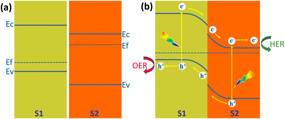 | ||
| Fig. 19 Schematic diagram of the energy band diagram of a Type II heterojunction, (a) in the dark before contact, (b) under illumination after contact. | ||
1D Si nanostructures-based Type II heterostructure photoanodes were fabricated by using n-Si nanowires core and α-Bi2O3 shell and Sn3O4 nanosheets.139,140 Excellent PEC water splitting performance was achieved due to the enhanced light harvesting, efficient photogenerated electron–hole separation and rapid charge transfer at the photoanode. Although a Ag interlayer is introduced between the p-Si nanowire core and the semiconducting MoS2 shell, the charge transfer between Si and MoS2 follows the Type II mechanism.104 Ta2O5 and N-doped graphene quantum dots (NGQD) were sequentially decorated on the surface of the p-Si nanowires.141 As shown in Fig. 20a, the p-SiNWs-Ta2O5-NGQD photoelectrodes exhibited more positive onset potential and much higher photocurrents than p-Si nanowires and p-Si nanowires-NGQD. The photogenerated carriers transfer between Si and Ta2O5 and between Ta2O5 and NGQD follows the Type II mechanism, that is, a double Type II heterojunction is formed (Fig. 20b).
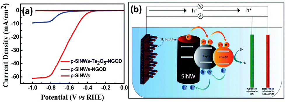 | ||
| Fig. 20 (a) PEC HER performance of the p-SiNWs-Ta2O5-NGQD photoelectrodes. (b) Schematic diagram of the charge transfer process in the p-SiNWs-Ta2O5-NGQD photoelectrode. Reproduced with permission from ref. 141, Copyright © The Royal Society of Chemistry 2022. | ||
Z-Scheme heterojunction
Type II heterojunctions do promote the separation of photogenerated carriers, but at the expense of the reducing capacity of photogenerated electrons and the oxidizing capacity of photogenerated holes. In this regard, Z-shaped heterojunctions are very beneficial for solar water splitting for hydrogen production. The Z-scheme junction is a heterojunction structure favourable for photoelectrochemical water splitting. The Z-scheme junction works similarly to the natural photosynthesis system. In terms of energy band structure, the Z-scheme heterojunction is similar to the type II heterojunction in that both are composed of two semiconductors with a staggered band alignment. However, the migration process of photogenerated carriers within Z-scheme heterojunctions is completely different from that of Type II heterojunctions due to the internal electric field, interfacial defects, and crystal facets.142Fig. 21 illustrates the schematic band diagram of a typical Z-scheme junction.138 To form a Z-scheme junction, the two semiconductors (S1 and S2) should have staggered alignment of band structures (Fig. 21a). When two semiconductors are in contact, electrons will flow from S1 to S2 because of the different Fermi levels until the Fermi levels of the two semiconductors are equal and equilibrium is reached. The energy bands of the two semiconductors are bent upward (S1) or downward (S2) at the interface. Under illumination, electrons jump from the valence band to the conduction band and create holes in the valence band. Driven by the built-in electric field generated by the energy band bending, the holes in the valence band of S1 and the electrons in the conduction band of S2 are transported to the interface and recombined (Fig. 21b). The electrons in the conduction band of S1 and holes in the valence band of S2 are transported to the surface of the semiconductor and undergo reduction and oxidation reactions, respectively. The recombination of electrons and holes at the interface of S1 and S2 significantly facilitates the separation and transfer of photogenerated carriers, thus improving their utilization. At the same time, the strong redox capacity of photogenerated electrons and photogenerated holes is maintained.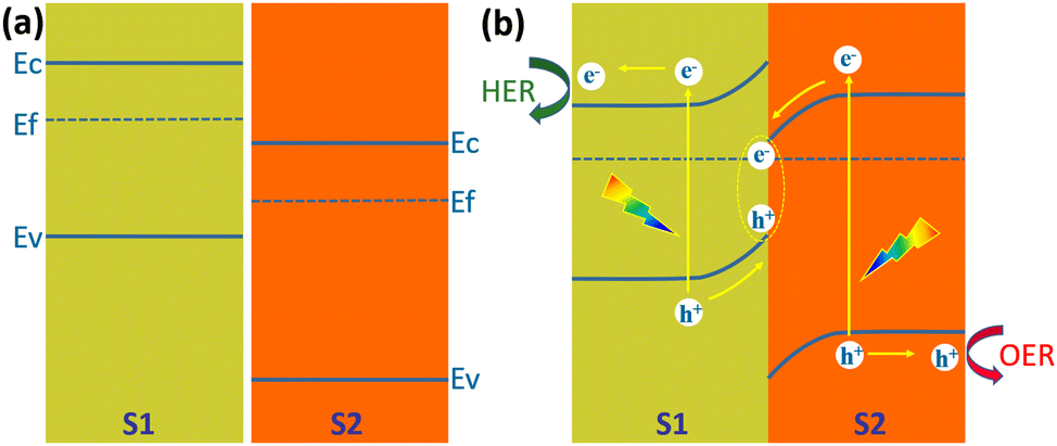 | ||
| Fig. 21 Schematic diagram of the energy band diagram of a Z-scheme heterojunction, (a) in the dark before contact, (b) under illumination after contact. | ||
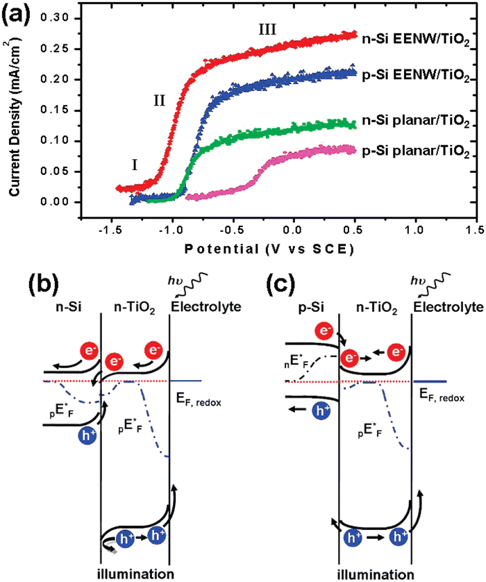
Yang et al. first realized the Z-scheme junction based on 1D Si nanostructures.143 The Si nanowires were prepared by the metal-assisted electroless etching method and then coated with conformal TiO2 film by atomic layer deposition (ALD). Fig. 22a shows that the heterojunction formed by n-Si nanowires and TiO2 has the best performance, exhibiting the lowest onset potential for OER and the largest photocurrents at the same potentials. The performance of nanowire photoelectrodes is better than that of planar photoelectrodes for both n-Si and p-Si, which benefits from the low reflectivity and large surface area. Compared with p-Si/TiO2, the photocurrent density of n-Si/TiO2 photoelectrodes is 20–25% higher, which benefits from the Z-scheme junction of n-Si/TiO2 that promotes photogenerated carrier separation. As shown in Fig. 22b, after the contact between n-Si and n-TiO2, the n-Si energy band bends upward, and the n-TiO2 energy band bends downward at the interface. Driven by the built-in electric field, the photogenerated holes in the n-Si valence band and the photogenerated electrons in the n-TiO2 conduction band move toward the interface and recombine at the interface. The holes in the valence band of n-TiO2 move to the surface to oxidize OH− to O2 (OER). The electrons in the n-Si conduction band flow through the external circuit to the counter electrode for HER. As for the p-Si/n-TiO2 structure, due to the lower Fermi energy level position of p-Si, the energy band bending direction of p-Si/n-TiO2 is exactly opposite to that of n-Si/n-TiO2 (Fig. 22c); thus the process as mentioned above of photogenerated carrier separation and transfer cannot occur, and the photocurrent is lowered.
 | ||
| Fig. 22 (a) PEC OER performance on different Si/TiO2 photoelectrodes. Band structures diagram of the n-Si/n-TiO2 (b) and p-Si/n-TiO2 heterostructures. Reproduced with permission from ref. 143, Copyright © 2009, American Chemical Society. | ||
Considering the very similar energy band structures of ZnO and TiO2, the formation of Z-scheme heterojunctions with ZnO and n-Si has also been investigated.144–146 It is worth mentioning that Peng et al. introduced Au nanoparticles acting as catalysts and plasma photosensitizers in the ZnO layer to achieve Au-sensitized n-Si/ZnO core–shell nanowire array photoanode for the unassisted water splitting.145 The doping of N in ZnO and the deposition of NiOOH co-catalyst on the ZnO surface also facilitate the performance of n-Si/ZnO 1D nanostructured array photoanodes for water splitting.146
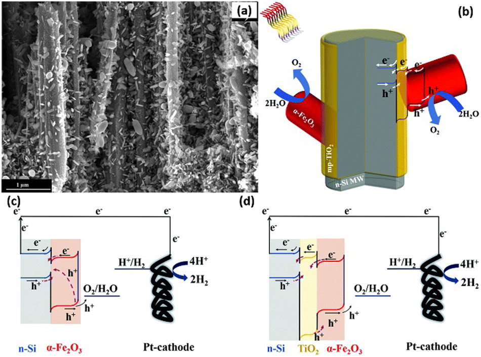
Wang and Peng et al. fabricated n-Si/Fe2O3 nanowire array photoelectrode, also based on the Z-scheme band alignment and charge transportation, to achieve an enhanced performance of the PEC OER.147,148 Qi et al. prepared n-Si/α-Fe2O3 core/shell nanowire arrays used as photoanode for PEC water splitting.149 The onset potential for OER was as low as 0.5 V vs. RHE, and the photocurrent was up to 5.28 mA cm−2 at a potential of 1.23 V vs. RHE. Fig. 23a clearly illustrates the energy band structure of n-Si/α-Fe2O3 and the separation and transfer process of photogenerated carriers under illumination. The thickness of the α-Fe2O3 layer on the Si surface is regulated by adjusting the concentration of iron nitrate in the preparation process. As shown in Fig. 23b, the different thickness of α-Fe2O3 significantly influences on the onset potential and current density of the photoelectrode. The onset potential becomes more positive with the increase of α-Fe2O3 thickness. Mott–Schottky test results show that the flat-band potential of the n-Si/α-Fe2O3 photoelectrodes increases with the increase of α-Fe2O3 thickness (Fig. 23c–f). This indicates that the band edge position of n-Si at the n-Si/α-Fe2O3 interface is higher in the samples with a smaller thickness of α-Fe2O3, so the quasi-Fermi energy level of the photogenerated electrons in n-Si is also higher after illumination. A smaller applied voltage is needed to assist the photogenerated electrons in n-Si to meet the energy required to reduce water to hydrogen. Hence, the onset potential of the photocurrent is more positive in the samples with a smaller thickness of α-Fe2O3. Researchers have proposed several methods to improve further the performance of the n-Si/α-Fe2O3 core/shell nanowire array photoelectrodes. NiO and Co3O4 co-catalysts were loaded on the α-Fe2O3 surface to improve the OER reaction kinetics.150 By doping α-Fe2O3 with Sn and forming oxygen vacancies, the charge transfer resistance is reduced, and the donor concentration is increased.151
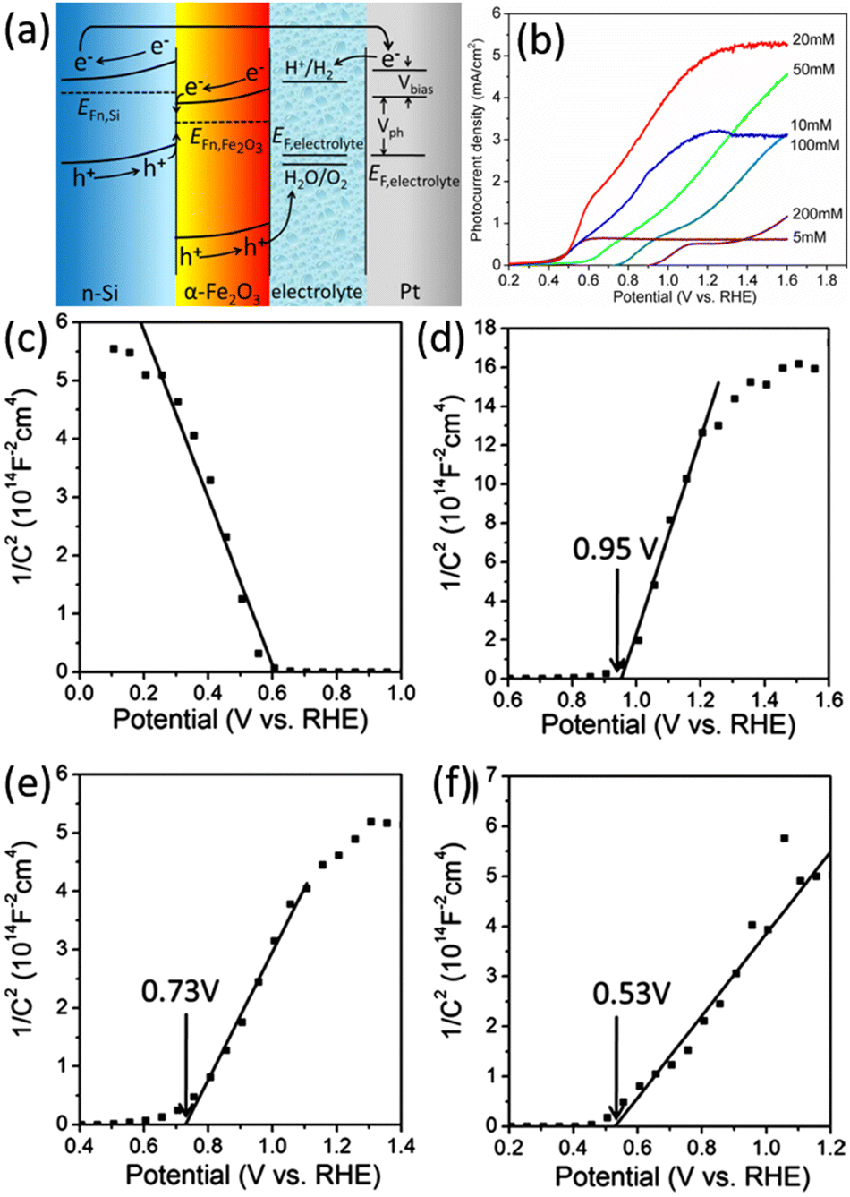 | ||
| Fig. 23 (a) Schematic band alignment of the n-Si/α-Fe2O3 heterostructure. (b) LSV curves of the n-Si/α-Fe2O3 core/shell nanowire arrays photoelectrodes prepared at different iron nitrate concentrations. Mott–Schottky curves recorded from photoelectrodes with different α-Fe2O3 thickness: (c) p-Si/α-Fe2O3-20 mM, (d) n-Si/α-Fe2O3-200 mM, (e) n-Si/α-Fe2O3-20 mM, (f) n-Si/α-Fe2O3-5 mM. Reproduced with permission from ref. 149, Copyright © The Royal Society of Chemistry 2014. | ||
The heterojunction formed by Si and other semiconductors effectively increases the photogenerated voltage of 1D Si photoelectrodes. However, the large number of defects at the Si/semiconductor interface will act as recombination centers and lead to recombination of the photogenerated carriers. A passivation layer has been introduced between Si and semiconductor to solve this problem. For example, an Al2O3 interlayer was inserted between n-Si and α-Fe2O3.152,153 Al2O3 can passivate the defects on the surface of Si microwires and the bottom surface of α-Fe2O3, promote the separation of photogenerated carriers and reduce the photoanode surface recombination rate. In addition, Al was doped into α-Fe2O3 to improve the charge transfer efficiency on the α-Fe2O3 surface. TiO2 interlayer was also introduced to the n-Si/α-Fe2O3 heterojunction.154,155 Solution-processed mesoporous TiO2 layer covered on the surface of the Si nanowires, and then α-Fe2O3 nanorods were grown on TiO2 through a hydrothermal method.155Fig. 24a and b show the SEM image and schematic diagram of the n-Si nanowires/TiO2/α-Fe2O3. It was found that the introduction of mesoporous TiO2 significantly enhanced the OER photocurrents of the photoelectrodes, which was attributed to the reduced charge recombination rate at the surface of α-Fe2O3, as illustrated in the band alignment of Fig. 24c and d.
 | ||
| Fig. 24 SEM image (a) and schematic diagram (b) of the n-Si nanowires/TiO2/α-Fe2O3. Band alignment of n-Si/α-Fe2O3 (c) and n-Si/TiO2/α-Fe2O3 (d). Reproduced with permission from ref. 155, Copyright © The Royal Society of Chemistry 2020. | ||
In addition, a 1D Si nanostructured heterojunction with a combined Z-scheme and Type II mechanism was also constructed. Liu et al. reported a multijunction of ZnIn2S4 nanosheet/TiO2 film/Si nanowire for PEC water splitting.156 Carrier transport between TiO2 and ZnIn2S4 follows the Type II mechanism, while carrier transport between TiO2 and Si follows the Z-scheme mechanism. The flat-band potential of the multi-junction becomes much more negative than that of the Si nanowire, indicating a higher carrier concentration and a more efficient charger transport process in the multi-junction. Furthermore, there are reports on the formation of Z-scheme heterojunctions of n-Si with other semiconductor materials, such as Si nanowires/WO3,157 Si nanowires/Co3O4,158etc.
Si/polymer heterojunction
In addition to inorganic semiconductors, 1D Si nanostructures can also form heterojunctions with semiconducting polymers. The Si/polymer heterojunctions offer advantages such as large-area coverage, low-temperature process capability, easy preparation, low cost, and so on.159 Zhang et al. reported the modification of Si nanowires with semiconducting polymers, including doped poly(3,4-ethylenedioxythiophene) (PEDOT)160,161 and poly((2,9,16,23-tetraaminophthalocyanine)Cu)) (CuTAPc).162 As shown in Fig. 25a, the Si/PEDOT junction helps separate the photogenerated carriers.160 The electrons transferred to the counter electrode for HER, and the holes transported to the surface of PEDOT to oxidize water with the assistance of the CuPc co-catalyst. As a result, the PEDOT/Si nanowire photoelectrodes exhibit significantly improved PEC performance (Fig. 25b). It was also reported that the methylation of Si could improve the PEC performance by dealing with the dangling bonds on Si, suppressing the carrier recombination, increasing the donor concentration, decreasing the charge transfer resistance, raising the flat band, and building a friendly and tight interface between the CH3-SiNWs array and PEDOT.163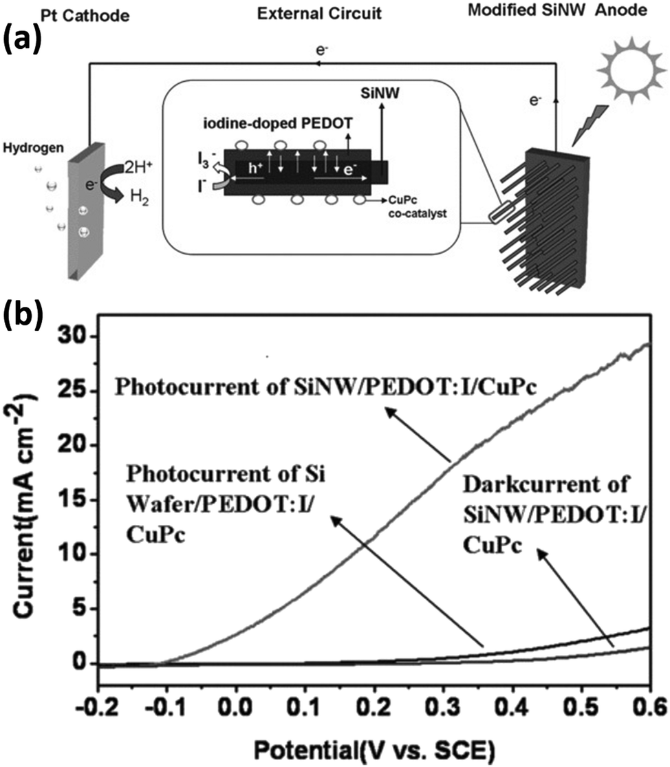 | ||
| Fig. 25 (a) Schematic diagram of the hydrogen-production PEC cell. (b) PEC performance comparison of the different photoelectrodes. Reproduced with permission from ref. 160, Copyright © 2012 Wiley-VCH Verlag GmbH & Co. KGaA, Weinheim. | ||
1D Si nanostructure homojunction
The narrow band gap of Si affords it excellent solar absorption properties but also determines the small photovoltage it can generate. As mentioned above, the use of other semiconductors to form heterojunctions with Si not only promotes the separation and transportation of photogenerated carriers, but also may compensate for the deficiencies caused by the energy level structure of Si. In addition to this, Si can be easily doped in different types and concentrations by well-established processes. With them, Si homojunctions (e.g., pn junctions, p–i–n junctions, etc.) can be constructed to substantially increase the photovoltage of Si-based devices, which have been successfully applied to solar cells. Nakato et al. reported that preparing a layer of heavily doped p+-Si (or n+-Si) on the surface of n-Si (or p-Si) can effectively increase the photovoltage of Si photoelectrodes and achieve PEC hydrogen production at a lower overpotential.164–166 This strategy has been applied to the 1D Si nanostructured photoelectrodes to increase the photovoltage and reduce the overpotential for PEC water splitting. Nathan S. Lewis et al. proposed the introduction of a buried metallurgical n+p junction into the Si wires.68,167Fig. 26a illustrates the preparation process of the n+p-Si wire arrays loaded with Pt co-catalysts.68 When p-Si comes into contact with the electrolyte, the chemical potential (Fermi level) of p-Si is different from that of the H+/H2 redox pair, and charge transfer between p-Si and the electrolyte occurs until equilibrium, and the energy band is bent downward by the formation of a depletion layer on the surface of p-Si, as shown in Fig. 26b. When intense light is illuminated to the p-Si/electrolyte system, the electrons and holes generated by photoexcitation are not transferred to the solution in time to be consumed or transferred to the Si interior. The newly generated net electrons will replenish the depletion layer, reducing the degree of band bending. The Fermi level splits into two “quasi-Fermi levels,” Ef,n and Ef,p, to describe the electrons and holes, respectively. The potential difference between Ef,n and Ef,p is the maximum photovoltage that the photoelectrode can generate. For the p-Si/n+-Si photoelectrodes, the Fermi energy level of n+-Si is consistent with the redox level of the H+/H2 couple because the surface n+-Si layer is heavily doped and degenerates at room temperature.165 The energy band structure of p-Si/n+-Si in contact with the electrolyte when it reaches equilibrium is shown in Fig. 26c. Under illumination, the potential difference between Ef,n and Ef,p is significantly larger than that of p-Si/electrolyte, indicating that p-Si/n+-Si/electrolyte can generate a higher photovoltage. It was confirmed that the photovoltage increased from 0.16 V to 0.54 V after introducing the n+-Si thin layer on the p-Si surface.68 Similarly, p–i–n junction Si nanowire arrays were prepared for photoelectrocatalytic water splitting for hydrogen production.168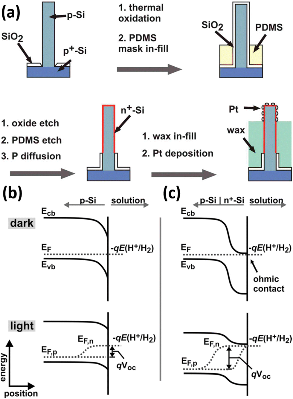 | ||
| Fig. 26 (a) Schematic diagram of the preparation process of Pt/n+p-Si wire arrays. Band bending of (b) p-Si and (c) n+p-Si photocathodes in contact with electrolyte. Reproduced with permission from ref. 68, Copyright © 2011, American Chemical Society. | ||
The photoelectrochemical properties of the Si nanowire arrays are averaged over numerous individual Si nanowires. Each Si nanowire may differ in geometry, doping, defects, and catalyst loading. This makes it challenging to correlate the average performance measured on the Si nanowire arrays well with these characteristics of the individual nanowires. In this regard, Yang et al. investigated the photoelectrochemistry of a single p-Si nanowire with an n+-Si thin layer on the surface.169 The Si nanowires were prepared by the VLS mechanism with a length of 8–20 μm and a diameter of 500–800 nm. The p-Si and n+p-Si nanowires were obtained by post-treatment of the Si nanowires and then loaded with Pt nanoparticles as co-catalysts. The PEC response curve shows that the HER onset potential of n+p-Si nanowires is more positive than that of p-Si. Statistical results for several single nanowires tested show that the HER onset potential of n+p-Si is positively shifted by about 250 mV.
By constructing buried pn junctions, increasing the photovoltage of 1D Si nanowire photoelectrodes is possible. However, the photovoltage generated by 1 pn junction is less than 0.6 V. The theoretical voltage for water splitting is 1.23 V, and the actual voltage required is as high as 1.7 V after considering the overpotential. To this end, Teitsworth et al. designed and fabricated Si nanowires encoded with p–i–n superlattice that can generate photovoltage of up to 10 V under 1 sun illumination.170 The Si nanowires were prepared by the VLS process. CoOx as OER catalyst and Pt as HER catalyst were modified at both ends of the Si nanowires to undergo water splitting, respectively. The photovoltage increased with the increasing number of p–i–n junctions, which was proved by the measurement of Si nanowires with various junctions. It was found that the photovoltage of a single junction is about 0.27 V. The photovoltage of the multijunction Si nanowires increases linearly with the number of p–i–n junctions. When the number of junctions was 40, the open-circuit voltage of the multijunction Si nanowire reached above 10 V under 1 sun illumination. Unassisted solar water splitting for hydrogen production was achieved based on such multi-junctional Si nanowires.
Conclusions and perspectives
1D Si nanostructured photoelectrodes have shown great potential in PEC water splitting for hydrogen production. It also has some problems, such as high overpotential due to poor catalytic activity and inappropriate energy band structure. Several strategies have been developed in recent years to reduce the overpotential of 1D Si nanostructured photoelectrodes for PEC water splitting. The modification of 1D Si nanostructures with co-catalysts, including noble metal catalysts (Pt, Ru, Ag, etc.), non-precious metal catalysts (Ni, Ni–Mo, NiCo, NiFe, etc.), MoSx (Mo3S4, MoS2, etc.) and other metal compounds (metal sulfides, metal phosphides, metal borides, metal oxides, etc.), carbon materials (N-doped graphene, reduced graphene oxide, carbon nanowires, etc.), could effectively improve the kinetics of the PEC water splitting reactions on the surface of 1D Si nanostructures and reduces the overpotential. Moreover, Si can also be combined with other semiconductor materials to construct 1D Si nanostructured heterojunction photoelectrodes, which can facilitate carrier utilization and enhance photovoltage through energy band engineering, and ultimately reduce overpotential for water splitting reaction. In addition, the construction of 1D Si nanostructured homojunctions has also been used to reduce the overpotential by increasing the photovoltage of the photoelectrode using the pn junction. In particular, multiple p–i–n junctions are formed in a single Si nanowire, and the photovoltage can be regulated by adjusting the number of p–i–n junctions, which can generate photovoltage up to 10 V. Using such multi-junction Si nanowires, hydrogen production from water under illumination without external voltage has been successfully achieved.Although significant progress has been achieved in reducing the overpotential of 1D nanostructured photoelectrodes for PEC hydrogen production, there are still many issues that deserve in-depth study. Currently, the modification of metals on the surface of 1D nanostructures is intended to be used as a co-catalyst to enhance the catalytic activity of the photoelectrodes. Schottky junctions formed by combining Si with metals can also be utilized to decrease the overpotential of the photoelectrodes. The choice of the appropriate metal and the proper modulation of the metal/Si interface can significantly increase the photovoltage.171–173 In addition, some highly promising catalysts emerging in recent years, such as high-entropy alloy catalysts,174 triple ionic-electronic conducting oxides,175 single-atom catalysts,176etc., have not yet been applied in 1D Si nanostructured photoelectrodes. These new catalysts may further enhance the performance of 1D Si nanostructured photoelectrodes.
The slow kinetics of the OER half-reaction leads to an increase in the overpotential for the overall water splitting reaction. To address this problem, replacing the OER reaction with other reactions with lower oxidation potential and faster reaction kinetics is an effective strategy to reduce the overpotential of PEC hydrogen production.4,177–179 Especially, coupling HER with some organic reactions that produce high-value chemicals can reduce the overpotential while lowering the cost of hydrogen production.180,181 Although this strategy has not yet been applied in 1D Si nanostructured photoelectrodes, we believe it would be an effective way to reduce the overpotential of 1D Si nanostructured photoelectrodes for solar hydrogen production and reduce the cost of hydrogen production, which would help to improve the competitiveness of solar hydrogen production technology compared with the conventional technologies.
Computational methods based on density functional theory have successfully predicted the catalytic activity of catalysts, explained catalytic phenomena, and found new high-performance catalysts.182–184 In addition, artificial intelligence (AI) techniques, which have emerged in recent years, are gradually being applied to materials and chemistry research fields.185,186 The importance of these new computational-based tools in scientific research is becoming increasingly evident. Applying these new technologies in 1D Si nanostructure photovoltaic research is rare. It is conceivable that the development and application of high-performance 1D Si nanostructured photoelectrodes could be significantly facilitated if theoretical computing and AI technologies are utilized and fully exploited.
Author contributions
This article was completed with the joint contribution of all authors. Guangwei She was responsible for the conceptualization and writing of the article. Xiaopeng Qi participated in the conception of the article and wrote and revised parts of it. Wensheng Shi was in overall charge of structuring and revising the article. Lixuan Mu was involved in discussing and revising parts of the article. Jingxuan Ma, Xue Hao, Changzhou Ru, and Haoyue Zhang conducted the literature review, analysis, and article revision.Conflicts of interest
There are no conflicts to declare.Acknowledgements
This work was supported by National Key R & D Program of China (2022YFB3803600) and the National Natural Science Foundation of China (21975269, 52172107).References
- Z. W. Seh, J. Kibsgaard, C. F. Dickens, I. Chorkendorff, J. K. Nørskov and T. F. Jaramillo, Science, 2017, 355, eaad4998 CrossRef PubMed.
- T. Hisatomi and K. Domen, Nat. Catal., 2019, 2, 387–399 CrossRef CAS.
- M. F. Lagadec and A. Grimaud, Nat. Mater., 2020, 19, 1140–1150 CrossRef CAS PubMed.
- X. M. C. Ta, R. Daiyan, T. K. A. Nguyen, R. Amal, T. Tran-Phu and A. Tricoli, Adv. Energy Mater., 2022, 12, 2201358 CrossRef CAS.
- M. Chatenet, B. G. Pollet, D. R. Dekel, F. Dionigi, J. Deseure, P. Millet, R. D. Braatz, M. Z. Bazant, M. Eikerling, I. Staffell, P. Balcombe, Y. Shao-Horn and H. Schäfer, Chem. Soc. Rev., 2022, 51, 4583–4762 RSC.
- G. Segev, J. Kibsgaard, C. Hahn, Z. J. Xu, W.-H. Cheng, T. G. Deutsch, C. Xiang, J. Z. Zhang, L. Hammarström, D. G. Nocera, A. Z. Weber, P. Agbo, T. Hisatomi, F. E. Osterloh, K. Domen, F. F. Abdi, S. Haussener, D. J. Miller, S. Ardo, P. C. McIntyre, T. Hannappel, S. Hu, H. Atwater, J. M. Gregoire, M. Z. Ertem, I. D. Sharp, K.-S. Choi, J. S. Lee, O. Ishitani, J. W. Ager, R. R. Prabhakar, A. T. Bell, S. W. Boettcher, K. Vincent, K. Takanabe, V. Artero, R. Napier, B. R. Cuenya, M. T. M. Koper, R. Van De Krol and F. Houle, J. Phys. D: Appl. Phys., 2022, 55, 323003 CrossRef.
- A. Aissa, N. A. A. Qasem, A. Mourad, H. Laidoudi, O. Younis, K. Guedri and A. Alazzam, Appl. Therm. Eng., 2023, 220, 119663 CrossRef CAS.
- A. Shah, P. Torres, R. Tscharner, N. Wyrsch and H. Keppner, Science, 1999, 285, 692–698 CrossRef CAS PubMed.
- H. Nishiyama, T. Yamada, M. Nakabayashi, Y. Maehara, M. Yamaguchi, Y. Kuromiya, Y. Nagatsuma, H. Tokudome, S. Akiyama, T. Watanabe, R. Narushima, S. Okunaka, N. Shibata, T. Takata, T. Hisatomi and K. Domen, Nature, 2021, 598, 304–307 CrossRef CAS PubMed.
- Q. Wang, C. Pornrungroj, S. Linley and E. Reisner, Nat. Energy, 2022, 7, 13–24 CrossRef.
- N. S. Lewis, Science, 2016, 351, aad1920 CrossRef PubMed.
- P. Zhou, I. A. Navid, Y. Ma, Y. Xiao, P. Wang, Z. Ye, B. Zhou, K. Sun and Z. Mi, Nature, 2023, 613, 66–70 CrossRef CAS PubMed.
- M. R. Shaner, H. A. Atwater, N. S. Lewis and E. W. McFarland, Energy Environ. Sci., 2016, 9, 2354–2371 RSC.
- A. Heller, Science, 1984, 223, 1141–1148 CrossRef CAS PubMed.
- A. J. Shih and S. M. Haile, Science, 2022, 376, 348–349 CrossRef CAS PubMed.
- H. Song, S. Luo, H. Huang, B. Deng and J. Ye, ACS Energy Lett., 2022, 7, 1043–1065 CrossRef CAS.
- K. Rajeshwar, R. McConnell and S. Licht, Solar hydrogen generation: toward a renewable energy future, Springer, 2008 Search PubMed.
- K. Sivula and R. van de Krol, Nat. Rev. Mater., 2016, 1, 15010 CrossRef CAS.
- A. Fujishima and K. Honda, Nature, 1972, 238, 37–38 CrossRef CAS PubMed.
- X. Qi, G. She, Y. Liu, L. Mu and W. Shi, Chem. Commun., 2012, 48, 242–244 RSC.
- L. Cheng, Q. Xiang, Y. Liao and H. Zhang, Energy Environ. Sci., 2018, 11, 1362–1391 RSC.
- X. Qi, G. She, M. Wang, L. Mu and W. Shi, Chem. Commun., 2013, 49, 5742–5744 RSC.
- C. A. Mesa, L. Francàs, K. R. Yang, P. Garrido-Barros, E. Pastor, Y. Ma, A. Kafizas, T. E. Rosser, M. T. Mayer, E. Reisner, M. Grätzel, V. S. Batista and J. R. Durrant, Nat. Chem., 2020, 12, 82–89 CrossRef CAS PubMed.
- T. W. Kim and K.-S. Choi, Science, 2014, 343, 990–994 CrossRef CAS PubMed.
- V. Andrei, G. M. Ucoski, C. Pornrungroj, C. Uswachoke, Q. Wang, D. S. Achilleos, H. Kasap, K. P. Sokol, R. A. Jagt, H. Lu, T. Lawson, A. Wagner, S. D. Pike, D. S. Wright, R. L. Z. Hoye, J. L. MacManus-Driscoll, H. J. Joyce, R. H. Friend and E. Reisner, Nature, 2022, 608, 518–522 CrossRef CAS PubMed.
- S. Hu, M. R. Shaner, J. A. Beardslee, M. Lichterman, B. S. Brunschwig and N. S. Lewis, Science, 2014, 344, 1005–1009 CrossRef CAS PubMed.
- D. Kang, J. L. Young, H. Lim, W. E. Klein, H. Chen, Y. Xi, B. Gai, T. G. Deutsch and J. Yoon, Nat. Energy, 2017, 2, 17043 CrossRef CAS.
- M. J. Kenney, M. Gong, Y. Li, J. Z. Wu, J. Feng, M. Lanza and H. Dai, Science, 2013, 342, 836–840 CrossRef CAS PubMed.
- Y. Li, Y. Xiao, C. Wu, D. Zhang, J. Huang, Z. Zhang, J. He and C. Li, ACS Mater. Lett., 2022, 4, 779–804 CrossRef CAS.
- K. Sun, S. Shen, Y. Liang, P. E. Burrows, S. S. Mao and D. Wang, Chem. Rev., 2014, 114, 8662–8719 CrossRef CAS PubMed.
- Z. M. Ronglei Fan and M. Shen, Opt. Express, 2019, A51–A80 Search PubMed.
- Z. Luo, T. Wang and J. Gong, Chem. Soc. Rev., 2019, 48, 2158–2181 RSC.
- S. Chandrasekaran, T. Nann and N. H. Voelcker, Nano Energy, 2015, 17, 308–322 CrossRef CAS.
- D. Liu, J. Ma, R. Long, C. Gao and Y. Xiong, Nano Today, 2017, 17, 96–116 CrossRef CAS.
- J.-W. Lee, K.-H. Cho, J.-S. Yoon, Y.-M. Kim and Y.-M. Sung, J. Mater. Chem. A, 2021, 9, 21576–21606 RSC.
- J. Deng, Y. Su, D. Liu, P. Yang, B. Liu and C. Liu, Chem. Rev., 2019, 119, 9221–9259 CrossRef CAS PubMed.
- J. M. Foley, M. J. Price, J. I. Feldblyum and S. Maldonado, Energy Environ. Sci., 2012, 5, 5203–5220 RSC.
- E. L. Warren, H. A. Atwater and N. S. Lewis, J. Phys. Chem. C, 2014, 118, 747–759 CrossRef CAS.
- B. Zhang, J. Jie, X. Zhang, X. Ou and X. Zhang, ACS Appl. Mater. Interfaces, 2017, 9, 34527–34543 CrossRef CAS PubMed.
- K.-Q. Peng, X. Wang, L. Li, Y. Hu and S.-T. Lee, Nano Today, 2013, 8, 75–97 CrossRef CAS.
- A. Jena, C.-J. Chen, H. Chang, S.-F. Hu and R.-S. Liu, J. Mater. Chem. A, 2021, 9, 3767–3785 RSC.
- S. A. Lee, S. Choi, C. Kim, J. W. Yang, S. Y. Kim and H. W. Jang, ACS Mater. Lett., 2020, 2, 107–126 CrossRef CAS.
- C. Cheng, W. Zhang, X. Chen, S. Peng and Y. Li, Energy Sci. Eng., 2022, 10, 1526–1543 CrossRef CAS.
- M. G. Walter, E. L. Warren, J. R. McKone, S. W. Boettcher, Q. Mi, E. A. Santori and N. S. Lewis, Chem. Rev., 2010, 110, 6446–6473 CrossRef CAS PubMed.
- E. M. Stuve, in Encyclopedia of Applied Electrochemistry, ed. G. Kreysa, K.-I. Ota and R. F. Savinell, Springer, New York, New York, NY, 2014, pp. 1445–1453 DOI:10.1007/978-1-4419-6996-5_330.
- S. L. S. David Tilley and Roel van de Krol, Advances in Photoelectrochemical Water Splitting: Theory, Experiment and Systems Analysis, The Royal Society of Chemistry, 2018 Search PubMed.
- R. Memming, Semiconductor Electrochemistry, Wiley-VCH Verlag GmbH, 2nd edn, 2015 Search PubMed.
- Semiconductor Electrodes and Photoelectrochemistry, ed. Allen J. Bard, M. Stratmann, S. Licht, 2002 Search PubMed.
- X. G. Zhang, Electrochemistry of Silicon and Its Oxide, Springer, 2001 Search PubMed.
- C. Huo, J. Wang, H. Fu, X. Li, Y. Yang, H. Wang, A. Mateen, G. Farid and K.-Q. Peng, Adv. Funct. Mater., 2020, 30, 2005744 CrossRef CAS.
- L. Liu, K.-Q. Peng, Y. Hu, X.-L. Wu and S.-T. Lee, Adv. Mater., 2014, 26, 1410–1413 CrossRef CAS PubMed.
- K. Peng, A. Lu, R. Zhang and S.-T. Lee, Adv. Funct. Mater., 2008, 18, 3026–3035 CrossRef CAS.
- K. Peng, M. Zhang, A. Lu, N.-B. Wong, R. Zhang and S.-T. Lee, Appl. Phys. Lett., 2007, 90, 163123 CrossRef.
- H. Chen, H. Wang, X.-H. Zhang, C.-S. Lee and S.-T. Lee, Nano Lett., 2010, 10, 864–868 CrossRef CAS PubMed.
- A. Mateen, G. Farid and K.-Q. Peng, ECS J. Solid State Sci. Technol., 2022, 11, 054006 CrossRef.
- K.-Q. Peng, X. Wang, L. Li, X.-L. Wu and S.-T. Lee, J. Am. Chem. Soc., 2010, 132, 6872–6873 CrossRef CAS PubMed.
- W. A. Bryant, J. Mater. Sci., 1977, 12, 1285–1306 CrossRef CAS.
- S. N. Mohammad, in Synthesis of Nanomaterials: Mechanisms, Kinetics and Materials Properties, ed. S. N. Mohammad, Springer International Publishing, Cham, 2020, pp. 69–99 DOI:10.1007/978-3-030-57585-4_5.
- V. Schmidt and U. Gösele, Science, 2007, 316, 698–699 CrossRef CAS PubMed.
- W. Lu and C. M. Lieber, J. Phys. D: Appl. Phys., 2006, 39, R387 CrossRef CAS.
- Y. Wu and P. Yang, J. Am. Chem. Soc., 2001, 123, 3165–3166 CrossRef CAS.
- B. M. Kayes, M. A. Filler, M. C. Putnam, M. D. Kelzenberg, N. S. Lewis and H. A. Atwater, Appl. Phys. Lett., 2007, 91, 103110 CrossRef.
- T. Shimizu, T. Xie, J. Nishikawa, S. Shingubara, S. Senz and U. Gösele, Adv. Mater., 2007, 19, 917–920 CrossRef CAS.
- R. Q. Zhang, Y. Lifshitz and S. T. Lee, Adv. Mater., 2003, 15, 635–640 CrossRef CAS.
- A. T. Heitsch, D. D. Fanfair, H.-Y. Tuan and B. A. Korgel, J. Am. Chem. Soc., 2008, 130, 5436–5437 CrossRef CAS PubMed.
- B. Fuhrmann, H. S. Leipner, H.-R. Höche, L. Schubert, P. Werner and U. Gösele, Nano Lett., 2005, 5, 2524–2527 CrossRef CAS PubMed.
- C.-M. Hsu, S. T. Connor, M. X. Tang and Y. Cui, Appl. Phys. Lett., 2008, 93, 133109 CrossRef.
- S. W. Boettcher, E. L. Warren, M. C. Putnam, E. A. Santori, D. Turner-Evans, M. D. Kelzenberg, M. G. Walter, J. R. McKone, B. S. Brunschwig, H. A. Atwater and N. S. Lewis, J. Am. Chem. Soc., 2011, 133, 1216–1219 CrossRef CAS PubMed.
- J. R. McKone, E. L. Warren, M. J. Bierman, S. W. Boettcher, B. S. Brunschwig, N. S. Lewis and H. B. Gray, Energy Environ. Sci., 2011, 4, 3573–3583 RSC.
- M. D. Kelzenberg, S. W. Boettcher, J. A. Petykiewicz, D. B. Turner-Evans, M. C. Putnam, E. L. Warren, J. M. Spurgeon, R. M. Briggs, N. S. Lewis and H. A. Atwater, Nat. Mater., 2010, 9, 239–244 CrossRef CAS PubMed.
- K. Peng, X. Wang and S.-T. Lee, Appl. Phys. Lett., 2008, 92, 163103 CrossRef.
- X. Wang, K.-Q. Peng, X.-J. Pan, X. Chen, Y. Yang, L. Li, X.-M. Meng, W.-J. Zhang and S.-T. Lee, Angew. Chem., Int. Ed., 2011, 50, 9861–9865 CrossRef CAS PubMed.
- J. Zhu, Z. Yu, G. F. Burkhard, C.-M. Hsu, S. T. Connor, Y. Xu, Q. Wang, M. McGehee, S. Fan and Y. Cui, Nano Lett., 2009, 9, 279–282 CrossRef CAS PubMed.
- K. Peng, Y. Yan, S. Gao and J. Zhu, Adv. Funct. Mater., 2003, 13, 127–132 CrossRef CAS.
- K. Peng, Y. Wu, H. Fang, X. Zhong, Y. Xu and J. Zhu, Angew. Chem., Int. Ed., 2005, 44, 2737–2742 CrossRef CAS PubMed.
- R. P. Srivastava and D.-Y. Khang, Adv. Mater., 2021, 33, 2005932 CrossRef CAS PubMed.
- J.-Y. Jung, Z. Guo, S.-W. Jee, H.-D. Um, K.-T. Park and J.-H. Lee, Opt. Express, 2010, 18, A286–A292 CrossRef CAS PubMed.
- S. Huang, H. Zhang, Z. Wu, D. Kong, D. Lin, Y. Fan, X. Yang, Z. Zhong, S. Huang, Z. Jiang and C. Cheng, ACS Appl. Mater. Interfaces, 2014, 6, 12111–12118 CrossRef CAS PubMed.
- X. Li, Y. Xiao, K. Zhou, J. Wang, S. L. Schweizer, A. Sprafke, J.-H. Lee and R. B. Wehrspohn, Phys. Chem. Chem. Phys., 2015, 17, 800–804 RSC.
- Y. J. Hwang, C. H. Wu, C. Hahn, H. E. Jeong and P. Yang, Nano Lett., 2012, 12, 1678–1682 CrossRef CAS PubMed.
- I. Oh, J. Kye and S. Hwang, Nano Lett., 2012, 12, 298–302 CrossRef CAS PubMed.
- Electrochemical Dictionary – 2nd, Revised and Extended Edition, ed. Allen J. Bard, G. Inzelt, F. Scholz, 2012 Search PubMed.
- J. K. Nørskov, T. Bligaard, A. Logadottir, J. R. Kitchin, J. G. Chen, S. Pandelov and U. Stimming, J. Electrochem. Soc., 2005, 152, J23 CrossRef.
- J. Ji, H. Zhang, Y. Qiu, Y. Wang, Y. Luo and L. Hu, J. Mater. Sci.: Mater. Electron., 2013, 24, 4433–4438 CrossRef CAS.
- L. Qiao, M. Zhou, Y. Li, A. Zhang, J. Deng, M. Liao, P. Xiao, Y. Zhang and S. Zhang, J. Electrochem. Soc., 2014, 161, H458–H463 CrossRef CAS.
- P. Dai, J. Xie, M. T. Mayer, X. Yang, J. Zhan and D. Wang, Angew. Chem., Int. Ed., 2013, 52, 11119–11123 CrossRef CAS PubMed.
- N. P. Dasgupta, C. Liu, S. Andrews, F. B. Prinz and P. Yang, J. Am. Chem. Soc., 2013, 135, 12932–12935 CrossRef CAS PubMed.
- L. Zhu, Q. Cai, F. Liao, M. Sheng, B. Wu and M. Shao, Electrochem. Commun., 2015, 52, 29–33 CrossRef CAS.
- F. Liao, B. Jiang, W. Shen, Y. Chen, Y. Li, Y. Shen, K. Yin and M. Shao, ChemCatChem, 2019, 11, 2126–2130 CrossRef CAS.
- U. Dadwal, N. Ranjan and R. Singh, AIP Conf. Proc., 2016, 1731, 050014 CrossRef.
- X. Gao, S. Wu, J. Yan, X. Zhai and X. Li, ACS Appl. Mater. Interfaces, 2016, 8, 30072–30078 CrossRef CAS PubMed.
- E. L. Warren, J. R. McKone, H. A. Atwater, H. B. Gray and N. S. Lewis, Energy Environ. Sci., 2012, 5, 9653–9661 RSC.
- M. R. Shaner, J. R. McKone, H. B. Gray and N. S. Lewis, Energy Environ. Sci., 2015, 8, 2977–2984 RSC.
- C.-W. Tung, C.-H. Hou, H.-T. Lin, Y. Zheng, Y.-P. Huang, Y.-F. Liao, J.-J. Shiue and H. M. Chen, Solar RRL, 2020, 4, 2000028 CrossRef CAS.
- W. Vijselaar, P. Westerik, J. Veerbeek, R. M. Tiggelaar, E. Berenschot, N. R. Tas, H. Gardeniers and J. Huskens, Nat. Energy, 2018, 3, 185–192 CrossRef CAS.
- C.-W. Tung, Y. Chuang, H.-C. Chen, T.-S. Chan, J.-Y. Li and H. M. Chen, Part. Part. Syst. Charact., 2018, 35, 1700321 CrossRef.
- T. F. Jaramillo, K. P. Jørgensen, J. Bonde, J. H. Nielsen, S. Horch and I. Chorkendorff, Science, 2007, 317, 100–102 CrossRef CAS PubMed.
- B. Hinnemann, P. G. Moses, J. Bonde, K. P. Jørgensen, J. H. Nielsen, S. Horch, I. Chorkendorff and J. K. Nørskov, J. Am. Chem. Soc., 2005, 127, 5308–5309 CrossRef CAS PubMed.
- P. D. Tran, S. S. Pramana, V. S. Kale, M. Nguyen, S. Y. Chiam, S. K. Batabyal, L. H. Wong, J. Barber and J. Loo, Chem. – Eur. J., 2012, 18, 13994–13999 CrossRef CAS PubMed.
- L. Zhang, C. Liu, A. B. Wong, J. Resasco and P. Yang, Nano Res., 2015, 8, 281–287 CrossRef CAS.
- L. Qiao, M. Liao, K. Fang, X. He and Y. Zhang, Silicon, 2019, 11, 1963–1970 CrossRef CAS.
- Q. Ding, F. Meng, C. R. English, M. Cabán-Acevedo, M. J. Shearer, D. Liang, A. S. Daniel, R. J. Hamers and S. Jin, J. Am. Chem. Soc., 2014, 136, 8504–8507 CrossRef CAS PubMed.
- S. M. Younan, Z. Li, M. P. Fairchild, N. B. Williams, Y. Huang and J. Gu, Adv. Mater. Interfaces, 2022, 9, 2200178 CrossRef CAS.
- L. Qiao, M. Liao, J. Wu, Q. Jiang, Y. Zhang and Y. Li, Int. J. Hydrogen Energy, 2018, 43, 22235–22242 CrossRef CAS.
- Z. Huang, C. Wang, L. Pan, F. Tian, X. Zhang and C. Zhang, Nano Energy, 2013, 2, 1337–1346 CrossRef CAS.
- G.-L. Zang, G.-P. Sheng, C. Shi, Y.-K. Wang, W.-W. Li and H.-Q. Yu, Energy Environ. Sci., 2014, 7, 3033–3039 RSC.
- S. H. Hsieh, S. T. Ho and W. J. Chen, J. Nanomater., 2016, 2016, 6974646 Search PubMed.
- X.-Q. Bao, D. Y. Petrovykh, P. Alpuim, D. G. Stroppa, N. Guldris, H. Fonseca, M. Costa, J. Gaspar, C. Jin and L. Liu, Nano Energy, 2015, 16, 130–142 CrossRef CAS.
- Y. Hou, B. L. Abrams, P. C. K. Vesborg, M. E. Björketun, K. Herbst, L. Bech, A. M. Setti, C. D. Damsgaard, T. Pedersen, O. Hansen, J. Rossmeisl, S. Dahl, J. K. Nørskov and I. Chorkendorff, Nat. Mater., 2011, 10, 434 CrossRef CAS PubMed.
- Z. Huang, C. Wang, Z. Chen, H. Meng, C. Lv, Z. Chen, R. Han and C. Zhang, ACS Appl. Mater. Interfaces, 2014, 6, 10408–10414 CrossRef CAS PubMed.
- C.-J. Chen, P.-T. Chen, M. Basu, K.-C. Yang, Y.-R. Lu, C.-L. Dong, C.-G. Ma, C.-C. Shen, S.-F. Hu and R.-S. Liu, J. Mater. Chem. A, 2015, 3, 23466–23476 RSC.
- S. Gopalakrishnan, G. Paulraj, M. K. Eswaran, A. Ray, N. Singh and K. Jeganathan, Chemosphere, 2022, 302, 134708 CrossRef CAS PubMed.
- E. J. Popczun, C. G. Read, C. W. Roske, N. S. Lewis and R. E. Schaak, Angew. Chem., Int. Ed., 2014, 53, 5427–5430 CrossRef CAS PubMed.
- J. Tian, Q. Liu, A. M. Asiri and X. Sun, J. Am. Chem. Soc., 2014, 136, 7587–7590 CrossRef CAS PubMed.
- X.-Q. Bao, M. F. Cerqueira, P. Alpuim and L. Liu, Chem. Commun., 2015, 51, 10742–10745 RSC.
- S. M. Thalluri, J. Borme, K. Yu, J. Xu, I. Amorim, J. Gaspar, L. Qiao, P. Ferreira, P. Alpuim and L. Liu, Nano Res., 2018, 11, 4823–4835 CrossRef CAS.
- C. W. Roske, E. J. Popczun, B. Seger, C. G. Read, T. Pedersen, O. Hansen, P. C. K. Vesborg, B. S. Brunschwig, R. E. Schaak, I. Chorkendorff, H. B. Gray and N. S. Lewis, J. Phys. Chem. Lett., 2015, 6, 1679–1683 CrossRef CAS PubMed.
- C. Lv, Z. Chen, Z. Chen, B. Zhang, Y. Qin, Z. Huang and C. Zhang, J. Mater. Chem. A, 2015, 3, 17669–17675 RSC.
- Z. Huang, Z. Chen, Z. Chen, C. Lv, H. Meng and C. Zhang, ACS Nano, 2014, 8, 8121–8129 CrossRef CAS PubMed.
- H. Zhang, Q. Ding, D. He, H. Liu, W. Liu, Z. Li, B. Yang, X. Zhang, L. Lei and S. Jin, Energy Environ. Sci., 2016, 9, 3113–3119 RSC.
- S. Lee, S. Cha, Y. Myung, K. Park, I. H. Kwak, I. S. Kwon, J. Seo, S. A. Lim, E. H. Cha and J. Park, ACS Appl. Mater. Interfaces, 2018, 10, 33198–33204 CrossRef CAS PubMed.
- G. She, S. Zhang, S. Li, F. Qu, L. Mu and W. Shi, J. Photochem. Photobiol., A, 2018, 355, 55–59 CrossRef CAS.
- G. Yan, Y. Dong, T. Wu, S. Xing and X. Wang, ACS Appl. Mater. Interfaces, 2021, 13, 52912–52920 CrossRef CAS PubMed.
- S. Zhang, G. She, S. Li, M. Lixuan and S. Wensheng, Nanotechnology, 2018, 29, 035601 CrossRef PubMed.
- S. Zhang, G. She, L. Mu and W. Shi, Mater. Lett., 2017, 197, 131–134 CrossRef CAS.
- Y. Yang, M. Wang, P. Zhang, W. Wang, H. Han and L. Sun, ACS Appl. Mater. Interfaces, 2016, 8, 30143–30151 CrossRef CAS PubMed.
- S. Y. Kim, R. Sivasankaran, M. Arunachalam, G. H. Lee, D. H. Youn and S. H. Kang, J. Electrochem. Soc., 2021, 168, 066519 CrossRef CAS.
- S. Chandrasekaran, T. Nann and N. H. Voelcker, Nanomaterials, 2016, 6, 144 CrossRef PubMed.
- X. Zhang and J. He, J. Nanosci. Nanotechnol., 2018, 18, 5674–5678 CrossRef CAS PubMed.
- U. Sim, T.-Y. Yang, J. Moon, J. An, J. Hwang, J.-H. Seo, J. Lee, K. Y. Kim, J. Lee, S. Han, B. H. Hong and K. T. Nam, Energy Environ. Sci., 2013, 6, 3658–3664 RSC.
- U. Sim, J. Moon, J. An, J. H. Kang, S. E. Jerng, J. Moon, S.-P. Cho, B. H. Hong and K. T. Nam, Energy Environ. Sci., 2015, 8, 1329–1338 RSC.
- H. Meng, K. Fan, J. Low and J. Yu, Dalton Trans., 2016, 45, 13717–13725 RSC.
- J. Moon, U. Sim, D. J. Kim, H.-Y. Ahn, J. An, H. Ha, K. S. Choi, C. Jeon, J. Lee, K. T. Nam and B. H. Hong, Nanoscale, 2018, 10, 13936–13941 RSC.
- R. R. Devarapalli, C. K. Kamaja and M. V. Shelke, J. Mater. Chem. A, 2014, 2, 13352–13358 RSC.
- Z. Chen, G. Ma, Z. Chen, Y. Zhang, Z. Zhang, J. Gao, Q. Meng, M. Yuan, X. Wang, J.-M. Liu and G. Zhou, Appl. Surf. Sci., 2017, 396, 609–615 CrossRef CAS.
- S. Gopalakrishnan, G. M. Bhalerao and K. Jeganathan, J. Power Sources, 2019, 413, 293–301 CrossRef CAS.
- S. Gopalakrishnan, G. M. Bhalerao and K. Jeganathan, ACS Sustainable Chem. Eng., 2019, 7, 13911–13919 CrossRef CAS.
- S. Bai, J. Jiang, Q. Zhang and Y. Xiong, Chem. Soc. Rev., 2015, 44, 2893–2939 RSC.
- W. Baicheng, X. Fenghua and X. Jianguang, Nanotechnology, 2014, 25, 455402 CrossRef.
- R. Yang, Y. Ji, Q. Li, Z. Zhao, R. Zhang, L. Liang, F. Liu, Y. Chen, S. Han, X. Yu and H. Liu, Appl. Catal., B, 2019, 256, 117798 CrossRef CAS.
- S. Riyajuddin, J. Sultana, S. A. Siddiqui, S. Kumar, D. Badhwar, S. S. Yadav, S. Goyal, A. Venkatesan, S. Chakraverty and K. Ghosh, Sustainable Energy Fuels, 2022, 6, 197–208 RSC.
- X. Li, C. Garlisi, Q. Guan, S. Anwer, K. Al-Ali, G. Palmisano and L. Zheng, Mater. Today, 2021, 47, 75–107 CrossRef CAS.
- Y. J. Hwang, A. Boukai and P. Yang, Nano Lett., 2009, 9, 410–415 CrossRef CAS PubMed.
- M. Shi, X. Pan, W. Qiu, D. Zheng, M. Xu and H. Chen, Int. J. Hydrogen Energy, 2011, 36, 15153–15159 CrossRef CAS.
- F.-Q. Zhang, Y. Hu, R.-N. Sun, H. Fu and K.-Q. Peng, Front. Chem., 2019, 7, 206 CrossRef CAS PubMed.
- I. V. Bagal, M. Arunachalam, A. Abdullah, A. Waseem, M. A. Kulkarni, S. Hyung Kang and S.-W. Ryu, J. Energy Chem., 2022, 71, 45–55 CrossRef CAS.
- M. T. Mayer, C. Du and D. Wang, J. Am. Chem. Soc., 2012, 134, 12406–12409 CrossRef CAS PubMed.
- X. Wang, K.-Q. Peng, Y. Hu, F.-Q. Zhang, B. Hu, L. Li, M. Wang, X.-M. Meng and S.-T. Lee, Nano Lett., 2013, 14, 18–23 CrossRef PubMed.
- X. Qi, G. She, X. Huang, T. Zhang, H. Wang, L. Mu and W. Shi, Nanoscale, 2014, 6, 3182–3189 RSC.
- R. R. Devarapalli, C. K. Kamaja and M. V. Shelke, ChemistrySelect, 2017, 2, 2544–2551 CrossRef CAS.
- Z. Zhou, S. Wu, L. Qin, L. Li, L. Li and X. Li, J. Mater. Chem. A, 2018, 6, 15593–15602 RSC.
- Y. Qu, F. Li, P. Zhang, L. Zhao, J. Liu, X. Song and L. Gao, Appl. Surf. Sci., 2019, 471, 528–536 CrossRef CAS.
- Z. Zhou, L. Li, Y. Niu, H. Song, X.-S. Xing, Z. Guo and S. Wu, Dalton Trans., 2021, 50, 2936–2944 RSC.
- W. Zhang, H. Chen, L. Zhang, P. Zhang, E. Dong, J. Ma and G. Wang, J. Alloys Compd., 2019, 773, 597–604 CrossRef CAS.
- A. Kawde, A. Annamalai, A. Sellstedt, J. Uhlig, T. Wågberg, P. Glatzel and J. Messinger, Phys. Chem. Chem. Phys., 2020, 22, 28459–28467 RSC.
- Q. Liu, F. Wu, F. Cao, L. Chen, X. Xie, W. Wang, W. Tian and L. Li, Nano Res., 2015, 8, 3524–3534 CrossRef CAS.
- Z. Chen, M. Ning, G. Ma, Q. Meng, Y. Zhang, J. Gao, M. Jin, Z. Chen, M. Yuan, X. Wang, J.-M. Liu and G. Zhou, Nanotechnology, 2017, 28, 275401 CrossRef PubMed.
- K.-Q. Lu, X. Lin, Z.-R. Tang and Y.-J. Xu, Catal. Today, 2019, 335, 294–299 CrossRef CAS.
- S.-C. Shiu, J.-J. Chao, S.-C. Hung, C.-L. Yeh and C.-F. Lin, Chem. Mater., 2010, 22, 3108–3113 CrossRef CAS.
- T. Yang, H. Wang, X.-M. Ou, C.-S. Lee and X.-H. Zhang, Adv. Mater., 2012, 24, 6199–6203 CrossRef CAS PubMed.
- C. Duan, H. Wang, X. Ou, F. Li and X. Zhang, ACS Appl. Mater. Interfaces, 2014, 6, 9742–9750 CrossRef CAS PubMed.
- Z. Liu, H. Wang, X.-M. Ou, C.-S. Lee and X.-H. Zhang, Chem. Commun., 2012, 48, 2815–2817 RSC.
- X. Zhang and J. He, J. Nanosci. Nanotechnol., 2018, 18, 2844–2849 CrossRef CAS PubMed.
- Y. Nakato, A. Tsumura and H. Tsubomura, Chem. Lett., 1982, 1071–1074 CrossRef CAS.
- Y. Nakato, Y. Egi, M. Hiramoto and H. Tsubomura, J. Phys. Chem., 1984, 88, 4218–4222 CrossRef CAS.
- Y. Nakato, M. Yoshimura, M. Hiramoto, A. Tsumura, T. Murahashi and H. Tsubomura, Bull. Chem. Soc. Jpn., 1984, 57, 355–360 CrossRef CAS.
- M. R. Shaner, M. T. McDowell, A. Pien, H. A. Atwater and N. S. Lewis, J. Electrochem. Soc., 2016, 163, H261–H264 CrossRef CAS.
- S. Riyajuddin, S. Kumar, D. Badhwar, S. A. Siddiqui, J. Sultana and K. Ghosh, Sustainable Energy Fuels, 2021, 5, 3160–3171 RSC.
- Y. Su, C. Liu, S. Brittman, J. Tang, A. Fu, N. Kornienko, Q. Kong and P. Yang, Nat. Nano, 2016, 11, 609–612 CrossRef CAS PubMed.
- T. S. Teitsworth, D. J. Hill, S. R. Litvin, E. T. Ritchie, J.-S. Park, J. P. Custer, A. D. Taggart, S. R. Bottum, S. E. Morley, S. Kim, J. R. McBride, J. M. Atkin and J. F. Cahoon, Nature, 2023, 614, 270–274 CrossRef CAS PubMed.
- H. Zhang, G. She, J. Xu, S. Li, Y. Liu, J. Luo and W. Shi, J. Mater. Chem. A, 2022, 10, 4952–4959 RSC.
- S. Li, H. Zhang, G. She, J. Xu, S. Zhang, Y. Deng, L. Mu, Q. Zhou, Y. Liu, J. Luo and W. Shi, ACS Appl. Energy Mater., 2021, 4, 11574–11579 CrossRef CAS.
- S. Li, G. She, J. Xu, S. Zhang, H. Zhang, L. Mu, C. Ge, K. Jin, J. Luo and W. Shi, ACS Appl. Mater. Interfaces, 2020, 12, 39092–39097 CrossRef CAS PubMed.
- Y. Luo, Z. Zhang, M. Chhowalla and B. Liu, Adv. Mater., 2022, 34, 2108133 CrossRef CAS PubMed.
- M. Papac, V. Stevanović, A. Zakutayev and R. O’Hayre, Nat. Mater., 2021, 20, 301–313 CrossRef CAS PubMed.
- L. Zhang, Y. Ren, W. Liu, A. Wang and T. Zhang, Natl. Sci. Rev., 2018, 5, 653–672 CrossRef CAS.
- B. Mei, G. Mul and B. Seger, Adv. Sustainable Sys., 2017, 1, 1600035 CrossRef.
- A. Y. Ru Ng, B. Boruah, K. F. Chin, J. M. Modak and H. S. Soo, ChemNanoMat, 2020, 6, 185–203 CrossRef.
- Y. Xu and B. Zhang, ChemElectroChem, 2019, 6, 3214–3226 CrossRef CAS.
- G. Li, G. Han, L. Wang, X. Cui, N. K. Moehring, P. R. Kidambi, D.-E. Jiang and Y. Sun, Nat. Commun., 2023, 14, 525 CrossRef CAS PubMed.
- Z. Li, Y. Yan, S.-M. Xu, H. Zhou, M. Xu, L. Ma, M. Shao, X. Kong, B. Wang, L. Zheng and H. Duan, Nat. Commun., 2022, 13, 147 CrossRef CAS PubMed.
- A. Jain, Y. Shin and K. A. Persson, Nat. Rev. Mater., 2016, 1, 15004 CrossRef CAS.
- J. K. Nørskov, T. Bligaard, J. Rossmeisl and C. H. Christensen, Nat. Chem., 2009, 1, 37–46 CrossRef PubMed.
- J. Resasco, F. Abild-Pedersen, C. Hahn, Z. Bao, M. T. M. Koper and T. F. Jaramillo, Nat. Catal., 2022, 5, 374–381 CrossRef.
- A. Mazheika, Y.-G. Wang, R. Valero, F. Viñes, F. Illas, L. M. Ghiringhelli, S. V. Levchenko and M. Scheffler, Nat. Commun., 2022, 13, 419 CrossRef CAS PubMed.
- P.-L. Kang, Y.-F. Shi, C. Shang and Z.-P. Liu, Chem. Sci., 2022, 13, 8148–8160 RSC.
| This journal is © The Royal Society of Chemistry 2023 |