
Exploring the optoelectronic properties of SnSe: a new insight†
Manoj
Kumar
 abc,
Sanju
Rani
ab,
Pargam
Vashishtha
ad,
Govind
Gupta
ad,
Xu
Wang
*c and
V. N.
Singh
*ab
abc,
Sanju
Rani
ab,
Pargam
Vashishtha
ad,
Govind
Gupta
ad,
Xu
Wang
*c and
V. N.
Singh
*ab
aAcademy of Scientific and Innovative Research (AcSIR), Ghaziabad, Uttar Pradesh-201002, India
bIndian Reference Materials (BND) Division, CSIR-National Physical Laboratory, Dr. K. S. Krishnan Marg, New Delhi-110012, India. E-mail: singhvn@nplindia.org
cSchool of Engineering, RMIT University, VIC 3000, Australia. E-mail: xu.wang@rmit.edu.au
dSensor Device Metrology Division, CSIR-National Physical Laboratory, Dr. K. S. Krishnan Marg, New Delhi 110012, India
First published on 28th October 2022
Abstract
Tin selenide has established its sound presence among 2D materials. A recent trend in the thermoelectric application study of this material has led to ignoring its optoelectronic potential. Here, we are unraveling its optoelectronics (viz., photodetector and solar cell) potential. Oxidation of the chalcogenides seems to be a boon for tin selenide for its optoelectronic properties. Tin selenide annealed at 300 °C in the open air for different times (0.5, 1, and 1.5 h) shows three consecutive layers (viz. SnSe, SnSe2, and SnO2). After the open-air annealing of SnSe, an enhanced photo-response in the broad spectrum is observed. A spectral response in the broad range of 250–1250 nm is observed compared to unannealed SnSe. Annealing time can tune the response in the required region, such as the ultraviolet and near-infrared regions. A maximum of 0.125 mA W−1 responsivity in the ultraviolet region (355 nm) for 1.5 h annealed and ∼0.117 mA W−1 for 0.5 h annealed in the near-infrared region has been observed. The layers formed are naturally in the form of basic solar cell structures. Experimentally the solar cell efficiency obtained after annealing indicates a new area of exploration for SnSe. A solar cell simulation study (by the simulation program SCAPS-1D) showed that efficiency is very sensitive to the electron affinity of the SnSe2 layer and could reach up to 20.28% under some defined conditions. This fabrication technique for the solar cell can substitute a clean room facility for the fabrication. The open-air annealing led to a better device in terms of responsivity, stability against environmental conditions, and natural formation of the solar cell. Also, this is the first ever reported device that can be uniquely formed just by open-air annealing. Optimizations in the parameters may open a new door in the fabrication technology of solar cells.
Introduction
Opto-electronics is the core of material sciences in terms of its application like optical communication, robotics, wearable electronics, bio-imaging, etc.1–3 Conversion of the optical signal (photons) into the electrical output on a broader spectral range enhances its demand in video imaging, biomonitoring, etc.3–5 A photodetector should have a high responsivity, detectivity (high signal-to-noise ratio), fast response, and broad spectral response. Commercialized broadband photodetectors face low detectivity (like Si) and high costs of fabrication (like Si and GaN-based).5,6Tin selenide is one of the recently researched chalcogenide materials. Its multifunctional applications have recently attracted much attention7–12 and it has been highly researched for its thermoelectric properties.13–16 There are very few reports in the literature that focus on the photoconductive17–25 and photovoltaic26–30 properties of tin selenide due to the one-sided focus on thermoelectrics. Tin chalcogenides are highly sensitive to surface oxidation, even at room temperature.31 The response time and responsivity for SnSe vary from a few microseconds to a few tens of seconds and a few milli to thousands of A W−1, respectively.17,32 But these reports focus on the visible NIR region, for pure SnSe film, with heterostructures, nanowires, quantum dots, etc.18,32–35 A few reports emphasized the effect of annealing in an inert atmosphere in terms of improved crystallinity,36,37 but still, a comparison is missing. Gupta et al. recently reported the effect of annealing in an inert atmosphere on the photoconductive properties of SnSe2, which led to overall improved film performance when annealed at 150 °C.38 Inert atmosphere post-annealing or in situ annealing led to better crystallinity,36 reduced defect states,39 and enhanced absorption.29 Introducing defects in a controlled manner in SnSe related to Se vacancy or loss also improved the photoconductive performance of the SnSe in terms of response speed, responsivity, and covered spectral range.40
Oxidation of metal chalcogenides is considered to deteriorate their properties. Many strategies have been applied to protect the material from harmful environmental conditions, like protective layers coating,31 surface engineering, etc. Pataniya et al. showed the behavior of photodetection performance of SnSe quantum dots under vacuum and environmental conditions. Adsorbed oxygen effectively increased the dark current in the device by lowering the Fermi level but added oxygen defect states which enhanced the photocurrent via photogain due to the long-lived trapping of excited carriers. Photoresponsivity increased but at the cost of response time under environmental conditions other than a vacuum.32
A detailed study of the chemical and thermal stability was analyzed in our previous study.41 The current work studies the effect of annealing SnSe in the open air at 300 °C for different times (viz. 0.5, 1, and 1.5 hour). It led to the formation of three consecutive layers, viz., SnSe, SnSe2, and SnO2. It shows that annealing benefits the photoconductive properties and extends the spectral range covering the ultraviolet, visible, and near-infrared (UV-Vis-NIR) regions. Here oxidation of SnSe seems to be a boon for its optoelectronic applications, while it appears to be a bane for thermoelectric applications.42
In this work, the first section compares the spectral response of the unannealed and annealed SnSe, showing the annealing time's effect on the photoconductive performance. After annealing, the responsivity and detectivity of the devices improved with the additional benefits of improved stability against environmental conditions. Devices (1.5, 1, and 0.5 h annealed) showed maximum responsivity values of 0.125 mA W−1 under 355 nm, 0.095 mA W−1 under 1064 nm, and 0.117 mA W−1 under 1064 nm, respectively. Also, we are reporting the inherent nature of SnSe as a solar cell device because all the required structures, like the p-type absorber layer, n-type buffer layer, electron transport, and window layer, formed upon annealing. After the open-air annealing with controlled conditions, p-type SnSe, n-type SnSe2, and SnO2 as window layers formed.
Solar cell based on SnSe and Si had a maximum efficiency of around ∼6.44%43 and SnSe has the potential to reach up to 27.7%.44 Theoretical and experimental demonstration of the as-obtained solar cell device is presented. The simulation program SCAPS-1D was used for the theoretical investigation of the performance of the natural device. The experimental study was carried out by depositing SnSe thin film by thermal evaporation followed by open-air annealing at 300 °C for different times (viz. 0.5, 1, and 1.5 hours). Overall, such a technique opens a new door for solar cell fabrication, which doesn’t require any clean room facilities for solar module fabrication, proving to be very cost effective.
We are reporting the hidden efficacy of SnSe in photoconductive (PC) and photovoltaic (PV) devices in addition to its good performance in the thermoelectric field. This report is subdivided into two sections, with the PC and PV performance in the first and second sections, respectively.
Experimental details
A detailed description of the deposition of the film using the thermal evaporation method is given in ref. 41. The film is cut into 5 × 10 mm2 pieces and placed in a furnace at a temperature of 300 °C for one hour with a 2 °C min−1 ramp rate followed by natural cooling. Raman spectroscopy (Jobin-Yvon T 6400 triple monochromator, excitation wavelength provided by ionized argon 785 nm) was used to confirm the phases in the film in the range 50–400 cm−1.For PC mode
A probe setup station (S10 Triax probe station with Keithley 2450 source meter acquisition unit with an accuracy of 10 nA in current readings and 100 μs in response time assessment) was used to perform wavelength correlated bias and power-dependent photoresponse measurements. The system includes a laser source with varying power densities (355 nm, 532 nm, and 1064 nm). The spectral responses of the devices are measured in the darkroom using a 450 W Xenon Lamp. The effective area of the device for the PC measurements is taken as 0.04 mm2.For PV mode
Current, voltage is measured using the Keithley 4200 semiconductor characterization system. A solar simulator AM 1.5G (class AAA, Photo Emission Tech.) was used for illumination purposes.Device structure
The device structure can be explored after the open-air annealing at 300 °C for a given time. This type of solar cell structure can also be made by simply transferring the SnSe2 and SnO2 layers onto the SnSe (by taking the buffer layer as SnSe2 and the window layer as SnO2). Fig. 1 shows the transformation of SnSe into three consecutive layers after annealing, where the upper- and lower-sections show the PC and PV devices, respectively. With the annealing under defined conditions, the thickness of the SnSe layer decreases due to the thermal and chemical instability of SnSe under defined conditions.41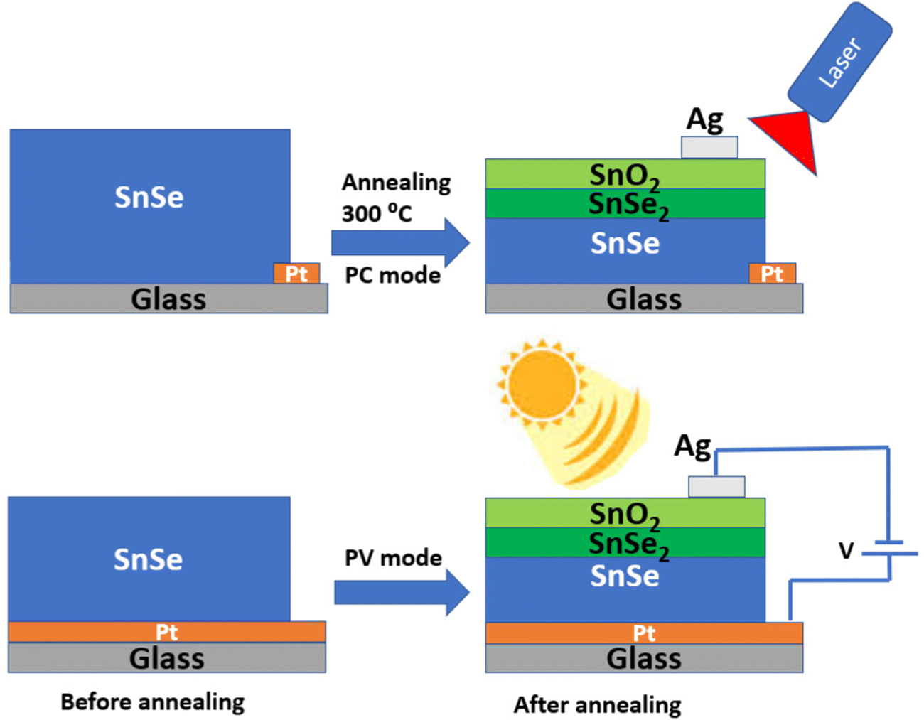 | ||
| Fig. 1 Upper and lower sections: device structures implemented by open-air annealing for PC and PV, respectively, of SnSe at 300 °C for a defined time. | ||
Results and discussions
Annealing in an inert atmosphere led to improved phases in terms of crystallinity and defects,36,37,45 but under open air led to changes and sometimes rearrangements of the phases in the material.41Phase evolution of the SnSe film on glass is studied using Raman spectroscopy when kept under an annealing condition of 300 °C for different times; the results are shown in Fig. 2(a) and (b). Raman is a bulk and surface-sensitive characterization technique due to its depth probing in bulk and sensitivity towards trace phases on the surface. The first three peaks of the Raman spectrum before annealing (Fig. 2(a)) match well with the previous report24 and show some sign of SnSe225 (labeled red in the figure) in the SnSe that may be due to the oxide formation at room temperature.31,46 In contrast, the SnO/SnO2 peak was not significant at room temperature, possibly due to the amorphous nature of the SnO/SnO2. Peak height and resolution can vary in the Raman spectrum due to using different excitation wavelengths in power laser irradiation, which may cause the lower peak intensity at 130 cm−1 corresponding to the A2g mode in unannealed SnSe.47
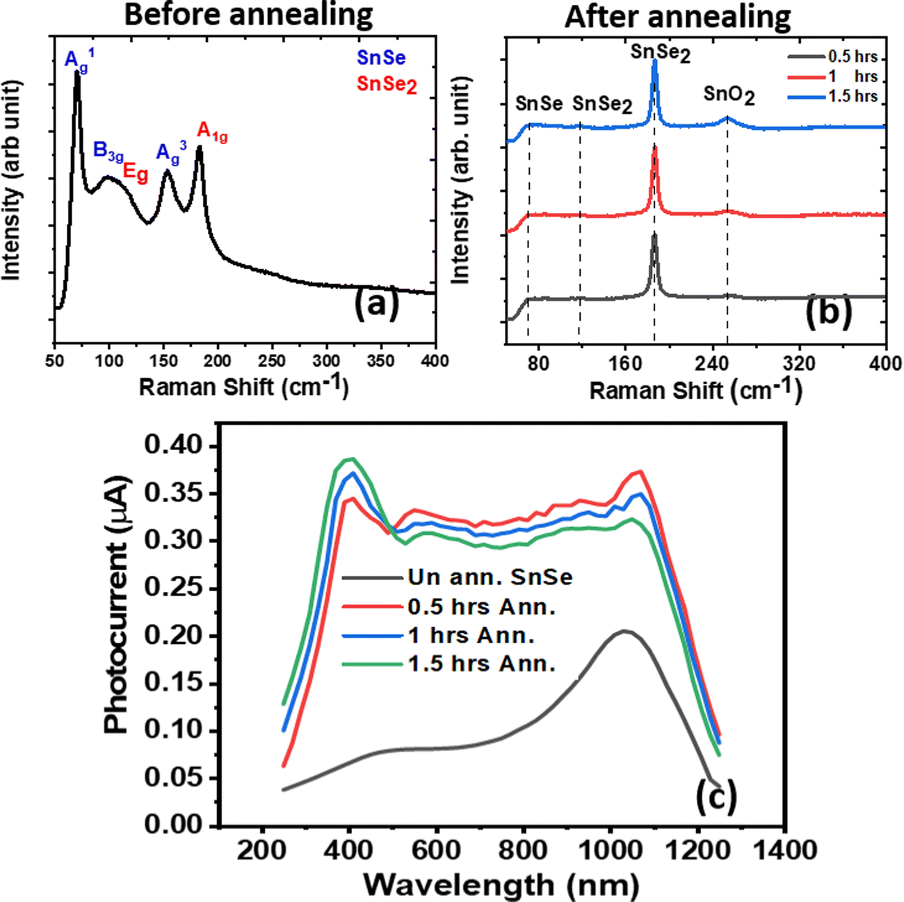 | ||
| Fig. 2 Raman spectra of SnSe (a) before and (b) after annealing, and (c) spectral response of the un-annealed and different time annealed SnSe at 300 °C. | ||
After annealing (Fig. 2(b)), a broad peak appears at ∼252 cm−1, corresponding to SnO2, which matches well with the literature.48 Also, it can be easily inferred that with increasing annealing time, the SnO2 peak height increases, which shows the increased and improved crystallinity of SnO2 due to elongated exposure to oxygen. As the peak corresponding to SnSe is significant at room temperature and only peaks of SnSe2 and SnO2 become intense at different stages of annealing, this implies that the SnSe phase is not present in the upper layers. Tin is more prone to oxide formation when heated and forms an oxide called SnO2.31 After the formation of oxides, plenty of Se atoms in SnSe remain ready to patch up the gaps. Due to the imbalance of the stoichiometric ratio of 1![[thin space (1/6-em)]](https://www.rsc.org/images/entities/char_2009.gif) :1 of Sn and Se, rearrangements of Se atoms happen, and SnSe2 is formed.31,46 A detailed mechanism of the appearance of these layers after annealing is discussed in our previous report.41 Raman spectroscopy was performed at randomly chosen spots on the sample to test the homogeneity of the structures in the device, and the results are shown in Fig. S1 (ESI†). From these spectra, one can conclude that the distribution of layers is homogeneous throughout the device.
:1 of Sn and Se, rearrangements of Se atoms happen, and SnSe2 is formed.31,46 A detailed mechanism of the appearance of these layers after annealing is discussed in our previous report.41 Raman spectroscopy was performed at randomly chosen spots on the sample to test the homogeneity of the structures in the device, and the results are shown in Fig. S1 (ESI†). From these spectra, one can conclude that the distribution of layers is homogeneous throughout the device.
Section 1. PC performance of the device
In our previous report, we have seen that different annealing temperature leads to an enhanced photoconductive (PC) performance of the SnSe, and annealing at 300 °C leads to broadband photoconduction.41I–V characteristics of the devices are shown in Fig. S2 (ESI†). Here different annealing time at 300 °C is studied, which shows that with the increase in the annealing time, an increment in the PC performance in the UV region is followed by a decrement in the PC performance in the NIR region. The spectral responses of the devices and their comparison with the unannealed SnSe are shown in Fig. 2(c). With the increasing annealing time, the crystallinity and thickness of the SnO2 layer increased, as confirmed by the Raman spectrum (Fig. 2(b)). So, UV response increases. Also, as the thickness of SnO2 increases, it is at the cost of a decrease in SnSe thickness because long exposure of Sn to oxygen leads to more SnO2 (from the surface to the depths of the film), and after the rearrangement of the Se atoms, the SnSe thickness decreases.The device's cyclic stability at different wavelengths (355, 532, and 1064 nm) was studied. PC measurements at 500 mV at 15 mW cm−2 power density are shown in Fig. 3(a)–(c). The very high stability of the PC performance over the entire selected spectra showed its suitability for the optoelectronic field.
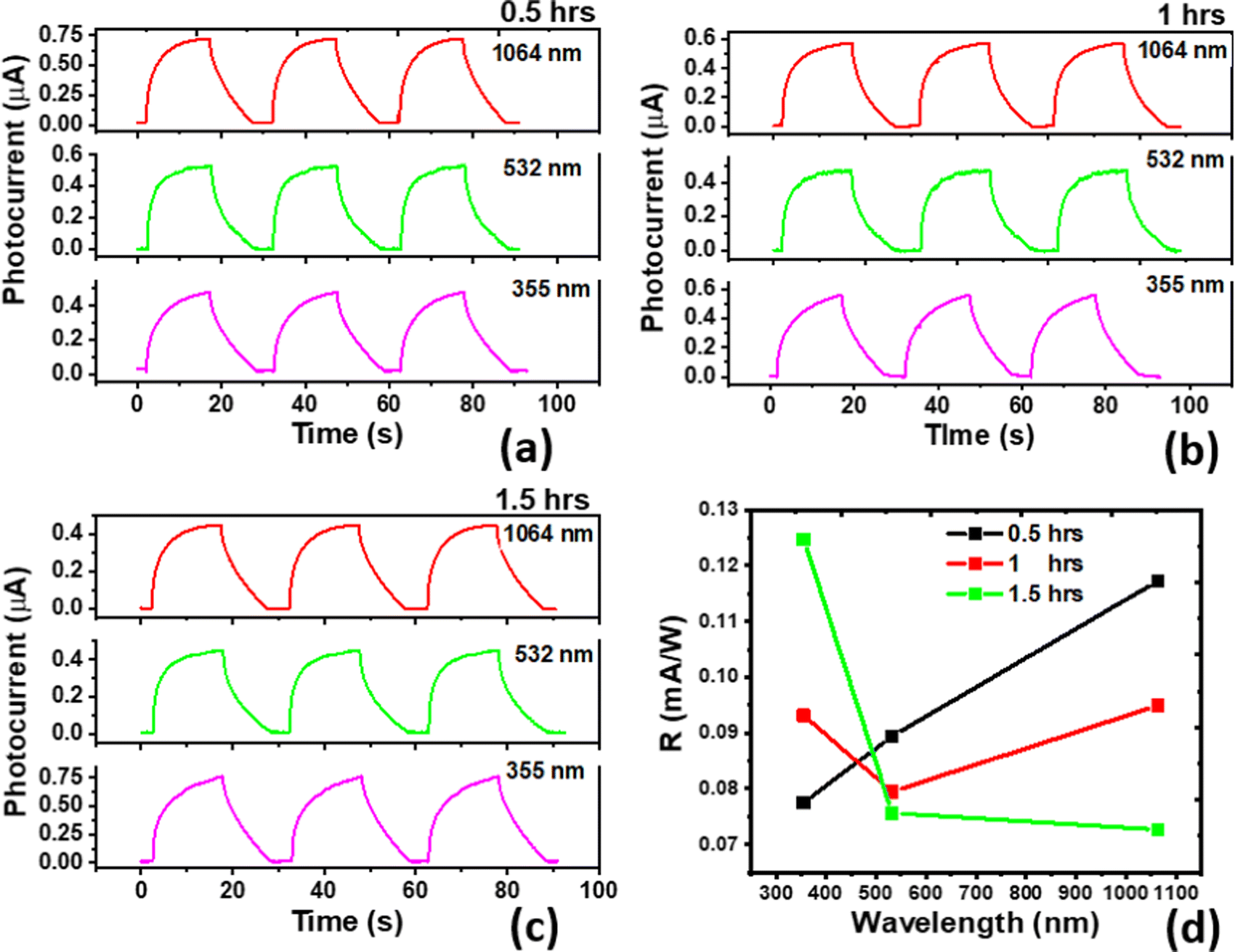 | ||
| Fig. 3 Cyclic stability (a)–(c) and responsivity (d) of the devices annealed at 300 °C for 0.5, 1, and 1.5 h, respectively, under 355, 532, and 1064 nm. | ||
The responsivities of the devices are shown in Fig. 3(d). Compared to our previous results of PC measurements on SnSe thin film,14 responsivity may be low due to the large effective area (∼20 times larger area) and different power densities used for these devices. Responsivity is sensitive to the effective area of the device and inversely proportional to the device's irradiated power density and effective area. Their relationship is given by 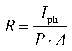 , where Iph, P, and A are the photocurrent, irradiated power density, and effective area of the device, respectively. A small area leads to a lower number of photons illuminated. Still, due to the trap/defect states in the device, it becomes important to minimize the spacing between electrodes for improved responsivity.
Also, the previous report22 on annealed samples at 300 °C showed nearly the same order for the photocurrent in the visible region, but for UV and IR, the current is enhanced by two orders. This discrepancy may be due to different effective areas, the contacts’ positions and nature, and the laser light's power density. The maximum detectivity of the device at 1.5 h annealed is 4.3 × 10¹⁰ Jones, the maximum among all the devices at 355 nm. Variation of the detectivity with the wavelength and the annealed time is shown in Fig. S3 (ESI†).
The rise and decay time fittings of the photocurrent at 1064 nm for 0.5, 1, and 1.5 h annealed devices are shown in Fig. S4 (ESI†). Response and recovery times of the 0.5, 1, and 1.5 h annealed devices are 4.80/8.19, 4.37/7.07, and 4.82/8.20 s, respectively, for 1064 nm illumination. In terms of rise time, all devices showed nearly the same time, while the recovery time showed that the 1 h annealed device has fewer defect/trap states than the others (0.5 and 1.5 h annealed). Thus, annealing for more than 1 h also led to increased defect states in the device, and 1 h of annealing seems to be an optimized time. It is observed that response time is greatly affected by the annealing, which may be due to the traps/defects arising in the device after annealing or, say, traps/defects dominated the photocurrent as compared to the original device in our previous work.24 Also a long exponential tail in the decay time confirms the supposition of the domination of trap/defect states in the device.49–51
Section 2. PV performance of the device
The present experimental solar cell efficiency is indicative of the idea's potential. The efficiencies of 0.05, 0.11, and 0.25% were obtained for the samples annealed for 0.5, 1, and 1.5 h, respectively. I–V characteristics of the devices under AM 1.5G solar radiation are shown in Fig. 4. A photograph of the solar cell device (film annealed for 1 h) is shown in Fig. S5 (ESI†). A detailed explanation of the cell efficiency is provided in the last part, along with the theoretical simulation results of the same solar cell structure. After annealing, the theoretical efficiency of the as-obtained system can reach up to ∼20%.
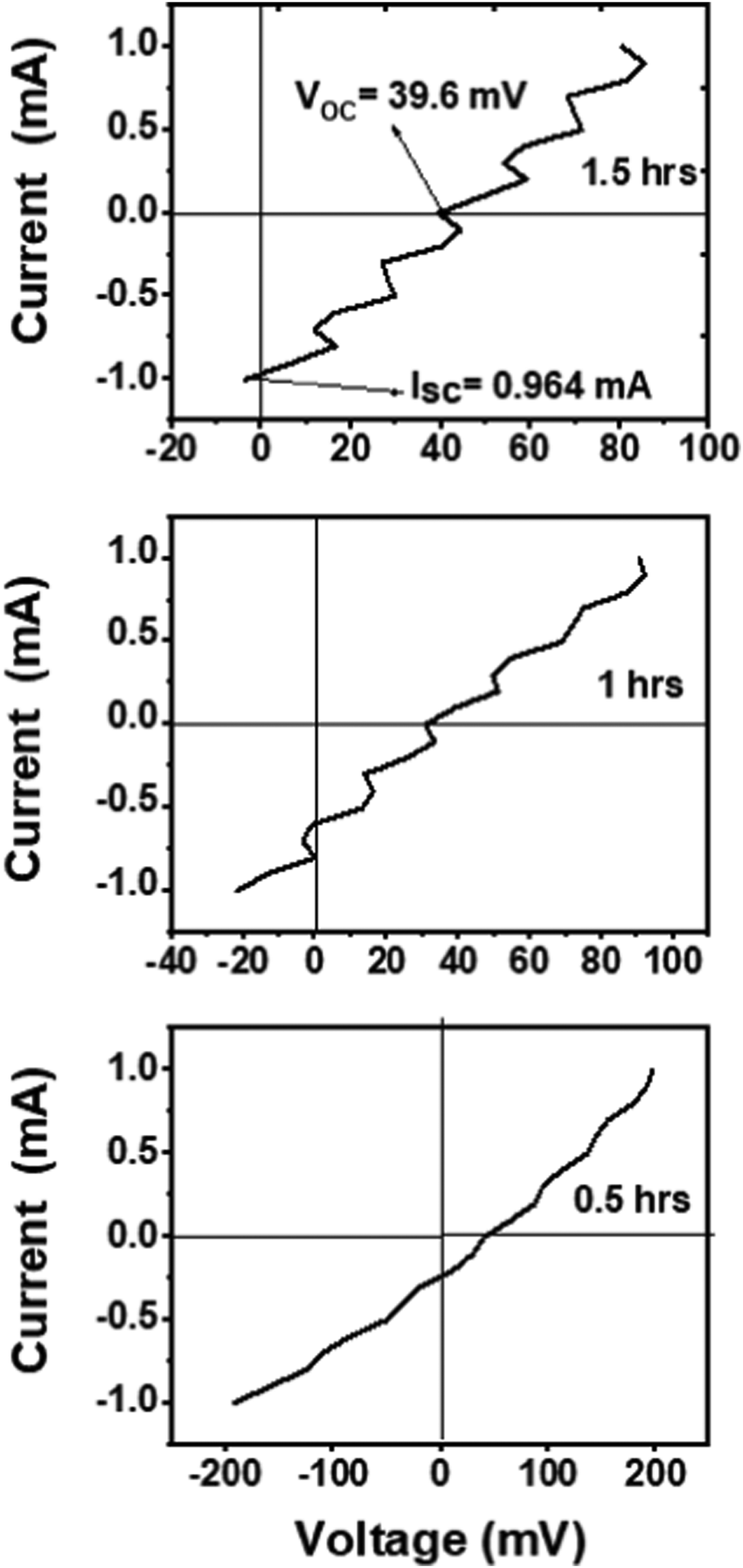 | ||
| Fig. 4 I–V characteristics of the solar cell devices under AM 1.5G optical power. | ||
Theoretical work
Simulation methodology
The performance of the SnSe/SnSe2/SnO2 cell is evaluated with the help of the SCAPS-1D software. Detailed studies about the program, algorithm, and equations for the electron and hole can be found in ref. 52–54.Results and discussion
The absorber layer is the most focused part of the solar cell. Many strategies are employed to enhance the efficiency of the solar cell after selecting the appropriate buffer layer. Buffer layer selection must guarantee the formation of the p–n junction. In the solar cell structure of SnSe/SnSe2/SnO2, the buffer layer (SnSe2) plays a vital role. The electron affinity of SnSe2 plays an important role in the efficiency of this solar cell. Generally, SnSe2 shows a very high work function 5.0 ± 0.1 eV.55,56 Roy et al.57 have reported 4.6 eV as the work function of SnSe2. D’Olimpio et al.58 reported that this discrepancy in the work function values is due to the surface oxidation of SnSe2 at room temperature, which leads to the formation of SnO2. Here we have varied the electron affinity of the SnSe2, which is very sensitive to surface oxidation, from 4.4 to 5.0 eV in steps of 0.2 eV as shown in Fig. 5(a) and (b) at valence band effective density of states (NV), conduction band effective density of states (NC), radiative recombination coefficient (RRC), electron and hole mobility of 1.8 × 1019 cm−3, 2.2 × 1018 cm−3, 1 × 10⁻⁶, 36.65 cm2 s−1 V−1 and 3.74 cm2 s−1 V−1, respectively.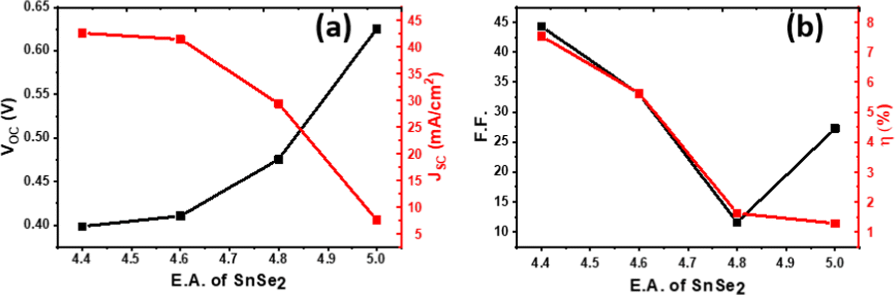 | ||
| Fig. 5 Effect of electron affinity on the parameters Voc, Jsc (a), FF, and efficiency (η) (b) of the SnSe-based solar device. | ||
With the increased electron affinity of the SnSe2, the efficiency of the cell decreased due to an increased notch in the band alignment of SnSe and SnSe2 that impedes the carrier collection.59 Efficiency increases from ∼1% to 7% when the electron affinity of SnSe2 decreases from 5.0 to 4.4 eV. Band alignment is shown in Fig. 6, where the electron affinity (E.A.) of SnSe2 is taken as 4.4 eV (Fig. 6(a)) and 5.0 eV (Fig. 6(b)). This schematic shows how this variation of the E.A. of SnSe2 impedes carrier transportation. For the increasing E.A. of the SnSe2, the height of the potential barrier between the SnSe and SnSe2 interface increases, and also formation of a potential well in the SnSe2 layer can be seen in Fig. 6. The sandwiched SnSe2 layer behaves like a potential well for the carriers. Hence the transportation of carriers is largely affected and hence the lower efficiency.
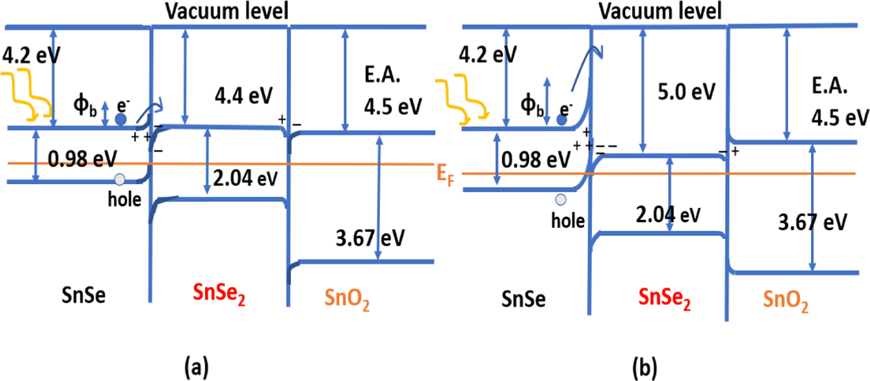 | ||
| Fig. 6 Schematic diagram of the band alignment of the configuration when the E.A. of SnSe2 is (a) 4.4 eV and (b) 5.0 eV. E.A. (5.0 eV) makes the barrier a greater height and creates a potential well in the transportation of the carriers. | ||
Also, by controlling the open-air annealing conditions, the thickness of the SnSe2 and SnO2 can be varied. With the increase in the annealing time or temperature, oxidation and hence the thickness of the SnSe2 and SnO2 can be varied. The long-time annealing may lead to the formation of a homogeneous oxide layer. After the oxidation of SnSe and the formation of SnO2, an imbalance in the stoichiometry ratio of Sn and Se atoms is created. Rearrangements of the Sn and Se atoms occur, leading to the formation of SnSe2 due to Sn deficiency.31,46 To study the device's sensitivity toward the thickness of the SnSe2/SnO2, we varied the thickness of these layers in the 25–100 nm range in steps of 25 nm, as shown in Fig. S6(a) and(b) (ESI†). Although the thickness of layers plays a vital role in the device in terms of homogeneity of the layers, cell efficiency seems insensitive to the thickness of the buffer and window layers. After optimizing the buffer and window layer parameters, when the absorber layer is optimized with selected parameters (NV, NC, RRC, electron and hole mobility of 2.2 × 1015 cm−3, 1.8 × 1016 cm−3, 1 × 10⁻⁶, 1000 cm2 s−1 V−1 and 100 cm2 s−1 V−1, respectively) given in the previous report44 (with 50 nm thickness for the SnSe2 and SnO2 layers), the efficiency of the cell reaches up to 20.28% (Fig. S7, ESI†).
At last, the solar cell based on SnSe/SnSe2/SnO2 can also be exploited with open-air annealing, where annealing conditions require more focused research so that a homogeneous layer of SnSe2 and SnO2 can be optimized. The electron affinity of the SnSe2 controls the device's overall performance and is also sensitive to oxidation, as inferred from the above section. Still, many defects/traps exist in the devices that impede their efficiency, as verified by the response time. More research must be done to optimize the annealing conditions (like annealing in a pure oxygen atmosphere for forming SnO2 or annealing under an inert atmosphere for better rearrangement of the atoms in the layers after open-air/controlled oxygen atmosphere annealing that could improve the E.A. of SnSe2) so that the electron affinity of SnSe2 can be tuned. Such a strategy will not only lead to a stable and self-powered photodetector but also the fabrication of the solar cell will lead to a stable and cheap device.
Conclusion
Tin selenide has immense potential as an optoelectronic material. Open-air annealing not only derived its hidden capacity in the PC mode but also in the PV mode. Robust, broadband PC mode can be tuned in the UV or IR region by selecting annealing conditions. The device annealed for 1 hour showed average behavior in the PC mode (although there is a slight variation in the parameters). The efficiency of the as-annealed SnSe indicates the hidden potential of SnSe. A more insightful study must be done to control the electron affinity of the SnSe2 that seems sensitive toward oxidation. As confirmed by the decay time calculation, the trap/defect states in the device are still a significant hurdle in its optoelectronics applications.Further improvement in the annealing conditions may improve the absorber and buffer layer properties, enhancing the PC and PV mode properties. Also, a simulation study showed that an efficiency of 20.27% can be obtained under certain conditions. Thus, a tin selenide solar cell structure can be obtained by open-air annealing, requiring fewer fabrication steps. Therefore, it can address the emerging demands for cheap and stable solar cells.
Data availability
Data will be made available upon request with proper justification.Conflicts of interest
The authors declare that they have no known competing financial interests or personal relationships that could have influenced the work reported in this paper.Acknowledgements
M. Kumar, S. Rani, and P. Vashishtha acknowledge the Council for Scientific and Industrial Research (CSIR), India, and UGC for the Senior Research Fellowship (SRF). The authors would like to thank Director CSIR-NPL for his constant support. We also thank Professor Burgelman of Gent University, Belgium, for providing the SCAPS program.References
- H. Guo, S. Saifi, K. Fukuda, H. M. Cheng, Z. Lou and X. Xu, Flexible organic photodetectors and their use in wearable systems, Digit. Signal Process.: Rev. J., 2022, 125, 103145, DOI:10.1016/j.dsp.2021.103145.
- Z. Zhao, J. Liu, Y. Liu and N. Zhu, High-speed photodetectors in optical communication system, J. Semicond., 2017, 38(12), 121001, DOI:10.1088/1674-4926/38/12/121001.
- W. W. Moses, Photodetectors for nuclear medical imaging, Nucl. Instrum. Methods Phys. Res., Sect. A, 2009, 610(1), 11–15, DOI:10.1016/j.nima.2009.05.032.
- F. Soldevila, E. Salvador-Balaguer, P. Clemente, E. Tajahuerce and J. Lancis, High-resolution adaptive imaging with a single photodiode, Sci. Rep., 2015, 5, 14300, DOI:10.1038/srep14300.
- N. Ding, et al., A novel approach for designing efficient broadband photodetectors expanding from deep ultraviolet to near infrared, Light: Sci. Appl., 2022, 11, 91, DOI:10.1038/s41377-022-00777-w.
- P. Vashishtha, L. Gowsami, K. S. Jain, N. Aggarwal and G. Gupta, GaN-djoser pyramidal self powered UV photodetector for optical signal detection in rugged environments, J. Alloys Compd., 2023, 930, 167267, DOI:10.1016/j.jallcom.2022.167267.
- M. Kumar, S. Rani, Y. Singh, S. Gour and V. Nand, Tin-selenide as a futuristic material: Properties and applications, RSC Adv., 2021, 11, 6477–6503, 10.1039/D0RA09807H.
- S. Rani, M. Kumar, Y. Singh, M. Tomar, A. Sharma, V. Gupta and V. N. Singh, NO2 gas sensor based on SnSe/SnSe2 p–n heterojunction, J. Nanosci. Nanotechnol., 2021, 21(9), 4779–4785, DOI:10.1166/jnn.2021.19278.
- S. Rani, M. Kumar, H. Sheoran, R. Singh and V. Nand, Rapidly responding room temperature NO2 gas sensor based on SnSe nanostructured film, Mater. Today Commun., 2022, 30(2), 103135, DOI:10.1016/j.mtcomm.2022.103135.
- S. Rani, et al., Temperature-dependent n–p–n switching and highly selective room-temperature n-SnSe2/p-SnO/n-SnSe heterojunction-based NO2 gas sensor, ACS Appl. Mater. Interfaces, 2022, 14, 15381–15390, DOI:10.1021/acsami.1c24679.
- M. Kumar, P. Sharma, S. Rani, M. Kumar and V. N. Singh, Ultrafast excited-state dynamics of SnSe2–SnSe composite thin film, AIP Adv., 2021, 11(2), 025040, DOI:10.1063/5.0038269.
- S. Rani, M. Kumar, Y. Singh and V. N. Singh, Au/Pd bimetallic nanoparticles decorated SnSe2 thin films for NO2 detection, J. Nanosci. Nanotechnol., 2021, 21(9), 4916–4920, DOI:10.1166/jnn.2021.19277.
- X. L. Shi, W. Y. Chen, X. Tao, J. Zou and Z. G. Chen, Rational structural design and manipulation advance SnSe thermoelectrics, Mater. Horiz., 2020, 7(12), 3065–3096, 10.1039/d0mh00954g.
- X. Y. Mao, et al., High thermoelectric and mechanical performance in the n-type polycrystalline SnSe incorporated with multi-walled carbon nanotubes, J. Mater. Sci. Technol., 2022, 114, 55–61, DOI:10.1016/j.jmst.2021.12.002.
- X. L. Shi, et al., A solvothermal synthetic environmental design for high-performance SnSe-based thermoelectric materials, Adv. Energy Mater., 2022, 12(20), 2200670, DOI:10.1002/aenm.202200670.
- M. Kumar, S. Rani, Y. Singh and V. N. Singh, Tuning the thermoelectric material’s parameter: a comprehensive review, J. Nanosci. Nanotechnol., 2020, 20(6), 3636–3646, DOI:10.1166/jnn.2020.17531.
- L. Hao, et al., 2D SnSe/Si heterojunction for self-driven broadband photodetectors, 2D Mater., 2019, 6, 034004 CrossRef CAS.
- D. Zheng, et al., High-performance near-infrared photodetectors based on p-type SnX (X = S, Se) nanowires grown via chemical vapor deposition, ACS Nano, 2018, 12(7), 7239–7245, DOI:10.1021/acsnano.8b03291.
- L. Hao, et al., Wafer-size growth of 2D layered SnSe films for UV-Visible-NIR photodetector arrays with high responsitivity, Nanoscale, 2020, 12(13), 7358–7365, 10.1039/d0nr00319k.
- H. Qiao, et al., Photoresponse improvement in liquid-exfoliated SnSe nanosheets by reduced graphene oxide hybridization, J. Mater. Sci., 2018, 53(6), 4371–4377, DOI:10.1007/s10853-017-1878-8.
- B. Ouyang, C. Chang, L. Zhao, Z. Lin and Y. Yang, Thermo-photoelectric coupled effect induced electricity in N-type SnSe:Br single crystals for enhanced self-powered photodetectors, Nano Energy, 2019, 66, 104111, DOI:10.1016/j.nanoen.2019.104111.
- L. Hao, et al., SnSe/SiO2/Si heterostructures for ultrahigh-sensitivity, ultrafast and broadband optical position sensitive detectors, IEEE Electron Device Lett., 2019, 40(1), 55–58, DOI:10.1109/LED.2018.2884325.
- M. Kumar, et al., Large area, self-powered, flexible, fast, and broadband photodetector enabled by the SnSe–Sb2Se3 heterostructure, Surf. Interfaces, 2022, 30, 101964, DOI:10.1016/j.surfin.2022.101964.
- M. Kumar, et al., Low bias operated, fast response SnSe thin-film Vis-NIR photodetector on glass substrate using one-step thermal evaporation technique, J. Alloys Compd., 2021, 879, 160370, DOI:10.1016/j.jallcom.2021.160370.
- M. Kumar, et al., Highly responsive, low-bias operated SnSe2 nanostructured thin film for trap-assisted NIR photodetector, J. Alloys Compd., 2020, 838, 155384, DOI:10.1016/j.jallcom.2020.155384.
- R. K. Singh and J. P. Bedi, FTO – SnSe heterojunction for photovoltaic conversion, 1991 Solar World Congress, 1992, pp. 447–451 DOI:10.1016/b978-0-08-041696-0.50081-4.
- P. Beltrán-Bobadilla, et al., SnSe solar cells: Current results and perspectives, Gen. Chem., 2021, 7(1), 200012, DOI:10.21127/yaoyigc20200012.
- V. R. Minnam Reddy, S. Gedi, B. Pejjai and C. Park, Perspectives on SnSe-based thin film solar cells: A comprehensive review, J. Mater. Sci.: Mater. Electron., 2016, 27(6), 5491–5508, DOI:10.1007/s10854-016-4563-9.
- N. Shahzad, et al., Annealed tin selenide (SnSe) thin film material for solar cell application, Chalcogenide Lett., 2020, 17(7), 347–351 CAS.
- Z. Li, et al., Effect of film thickness and evaporation rate on co-evaporated SnSe thin films for photovoltaic applications, RSC Adv., 2020, 10(28), 16749–16755, 10.1039/d0ra01749c.
- A. De Kergommeaux, J. Faure-Vincent, A. Pron, R. De Bettignies, B. Malaman and P. Reiss, Surface oxidation of tin chalcogenide nanocrystals revealed by 119Sn-Mössbauerspectroscopy, J. Am. Chem. Soc., 2012, 134(28), 11659–11666, DOI:10.1021/ja3033313.
- P. M. Pataniya, B. M. Soni, G. K. Solanki and V. Patel, Photodetector based on liquid phase exfoliated SnSe quantum dots, Opt. Mater., 2022, 125, 112110, DOI:10.1016/j.optmat.2022.112110.
- J. Liu, et al., High white light photosensitivity of SnSe nanoplate-graphene nanocomposites, Nanoscale Res. Lett., 2017, 12, 259, DOI:10.1186/s11671-017-2021-0.
- A. S. Pawbake, S. R. Jadkar and D. J. Late, High performance humidity sensor and photodetector based on SnSe nanorods, Mater. Res. Express, 2016, 3(10), 105038, DOI:10.1088/2053-1591/3/10/105038.
- H. Shantilal, A. Patel, J. Gohil and V. M. Pathak, Self-powered anisotropic photo-responsive properties of tin mono-selenide (SnSe) photodetector, Opt. Mater., 2022, 132, 112756, DOI:10.1016/j.optmat.2022.112756.
- R. Indirajith, M. Rajalakshmi, R. Gopalakrishnan and K. Ramamurthi, Effects of annealing on thermally evaporated SnSe thin films, Ferroelectrics, 2011, 413, 108–114, DOI:10.1080/00150193.2011.551090.
- D. Alagarasan, S. S. Hegde, S. Varadharajaperumal and K. D. A. Kumar, Effect of annealing temperature on SnS thin films for photodetector applications, J. Mater. Sci.: Mater. Electron., 2022, 33(8), 4794–4805, DOI:10.1007/s10854-021-07668-7.
- S. Umeshkumar Gupta, et al., Annealing induced phase transformation from amorphous to polycrystalline SnSe2 thin film photo detector with enhanced light-matter interaction, J. Non-Cryst. Solids, 2022, 578, 121353, DOI:10.1016/j.jnoncrysol.2021.121353.
- B. Sun, et al., Protected-annealing regulated defects to improve optical properties and luminescence performance of Ce:YAG transparent ceramics for white LEDs, J. Mater. Chem. C, 2019, 7, 4057–4065, 10.1039/c8tc06600k.
- F. Li, et al., Defect engineering in ultrathin SnSe nanosheets for high-performance optoelectronic applications, ACS Appl. Mater. Interfaces, 2021, 13, 33226–33236, DOI:10.1021/acsami.1c05254.
- M. Kumar, S. Rani, A. Kumar, J. Tawale and R. Srivastava, Broadband (NIR-Vis-UV) photoresponse of annealed SnSe films and effective oxidation passivation using Si protective layer, Mater. Res. Bull., 2022, 153, 111913, DOI:10.1016/j.materresbull.2022.111913.
- M. Zhang, D. Wang, C. Chang, T. Lin, K. Wang and L. D. Zhao, Oxygen adsorption and its influence on the thermoelectric performance of polycrystalline SnSe, J. Mater. Chem. C, 2019, 7(34), 10507–10513, 10.1039/c9tc03999f.
- K. F. A. El-Rahman, A. A. A. Darwish and E. A. A. El-Shazly, Electrical and photovoltaic properties of SnSe/Si heterojunction, Mater. Sci. Semicond. Process., 2014, 25, 123–129, DOI:10.1016/j.mssp.2013.10.003.
- M. Kumar, S. Rani, Y. Singh, A. Kumar and V. N. Singh, Strategy to improve the efficiency of tin selenide based solar cell: A path from 1.02 to 27.72%, Sol. Energy, 2022, 232, 146–153, DOI:10.1016/j.solener.2021.12.069.
- D. Alagarasan, et al., Optimization of different temperature annealed nanostructured CdSe thin film for photodetector applications, Opt. Mater., 2021, 122, 111706, DOI:10.1016/j.optmat.2021.111706.
- B. Zhang, et al., Dynamic epitaxial crystallization of SnSe2 on the oxidized SnSe surface and its atomistic mechanisms, ACS Appl. Mater. Interfaces, 2020, 12(24), 27700–27707, DOI:10.1021/acsami.0c05029.
- T. Sriv, T. Minh, H. Nguyen, Y. Lee, S. Y. Lim and V. Q. Nguyen, Optical phonons of SnSe(1−x)Sx layered semiconductor alloys, Sci. Rep., 2020, 10, 11761, DOI:10.1038/s41598-020-68744-2.
- M. N. Rumyantseva, et al., Raman surface vibration modes in nanocrystalline SnO2: Correlation with gas sensor performances, Chem. Mater., 2005, 17(4), 893–901 CrossRef CAS.
- B. Mallampati, S. V. Nair, H. E. Ruda and U. Philipose, Role of surface in high photoconductive gain measured in ZnO nanowire-based photodetector, J. Nanopart. Res., 2015, 17, 176, DOI:10.1007/s11051-015-2973-x.
- H. K. Yadav, K. Sreenivas and V. Gupta, Persistent photoconductivity due to trapping of induced charges in Sn/ZnO thin film based UV photodetector, Appl. Phys. Lett., 2010, 96(22), 223507, DOI:10.1063/1.3427417.
- M. Kumar, S. Rani, S. S. Kushvaha and V. N. Singh, Enhancing the performance of photodetector, Types of photodetectors and their applications, Nova science publication, USA, 2022, pp. 1–45 Search PubMed.
- M. Burgelman, P. Nollet and S. Degrave, Modelling polycrystalline semiconductor solar cells, Thin Solid Films, 2000, 361, 527–532, DOI:10.1016/S0040-6090(99)00825-1.
- K. Decock, S. Khelifi and M. Burgelman, Modelling multivalent defects in thin film solar cells, Thin Solid Films, 2011, 519(21), 7481–7484, DOI:10.1016/j.tsf.2010.12.039.
- K. Decock, P. Zabierowski and M. Burgelman, Modeling metastabilities in chalcopyrite-based thin film solar cells, J. Appl. Phys., 2012, 111(4), 043703, DOI:10.1063/1.3686651.
- M. I. Serna, et al., Low-temperature deposition of layered SnSe2 for heterojunction diodes, Adv. Mater. Interfaces, 2018, 5(16), 1800128, DOI:10.1002/admi.201800128.
- Q. Zhang, et al., Band offset and electron affinity of MBE-grown SnSe2, Appl. Phys. Lett., 2018, 112(4), 042108, DOI:10.1063/1.5016183.
- T. Roy, M. Tosun, M. Hettick, G. H. Ahn, C. Hu and A. Javey, 2D-2D tunneling field-effect transistors using WSe2/SnSe2 heterostructures, Appl. Phys. Lett., 2016, 108(8), 083111, DOI:10.1063/1.4942647.
- G. D’Olimpio, et al., Charge redistribution mechanisms in SnSe2 surfaces exposed to oxidative and humid environments and their related influence on chemical sensing, J. Phys. Chem. Lett., 2020, 11, 9003–9011, DOI:10.1021/acs.jpclett.0c02616.
- F. I. Za’abar, et al., A numerical investigation on the combined effects of MoSe2 interface layer and graded bandgap absorber in CIGS thin film solar cells, Coatings, 2021, 11, 930, DOI:10.3390/coatings11080930.
Footnote |
| † Electronic supplementary information (ESI) available. See DOI: https://doi.org/10.1039/d2tc03799h |
| This journal is © The Royal Society of Chemistry 2022 |