
Highly luminescent perovskite quantum dots for light-emitting devices: photopatternable perovskite quantum dot–polymer nanocomposites†
Cheng-Han
Sung
a,
Shi-Da
Huang
a,
Gautham
Kumar
 a,
Wen-Chi
Lin
a,
Chien-Chung
Lin
b,
Hao-Chung
Kuo
ac and
Fang-Chung
Chen
*ad
a,
Wen-Chi
Lin
a,
Chien-Chung
Lin
b,
Hao-Chung
Kuo
ac and
Fang-Chung
Chen
*ad
aDepartment of Photonics, College of Electrical and Computer Engineering, National Yang Ming Chiao Tung University, Hsinchu 30010, Taiwan. E-mail: fcchendop@nycu.edu.tw; fcchen@mail.nctu.edu.tw
bGraduate Institute of Photonics and Optoelectronics, Department of Electrical Engineering, National Taiwan University, Taipei 10617, Taiwan
cSemiconductor Research Center, Hon Hai Research Institute, Taipei 11492, Taiwan
dCenter for Emergent Functional Matter Science, National Yang Ming Chiao Tung University, Hsinchu 30010, Taiwan
First published on 11th October 2022
Abstract
In this study we synthesize organic–inorganic hybrid perovskite quantum dots (PeQDs) having a high photoluminescence quantum yield (PLQY = 98%) for light-emitting applications. The luminescence peak of the FAPbBr3 (FA+: formamidinium) PeQDs in solution is located at 527 nm; its CIE 1931 color coordinates are (0.169, 0.760), very close to the BT.2020 standard (0.170, 0.797). After mixing the PeQDs with polydimethylsiloxane, the mixture behaves as a color-conversion layer (CCL) for quantum-dot light emitting diodes (LEDs), achieving a high power efficiency (129.4 lm W−1). Because PeQDs readily decompose in most polar solvents, we blend ours with polyvinylcinnamate (PVCN), which is readily soluble in toluene, to formulate photopatternable thin films. The resulting photopatternable perovskite quantum dot–polymer nanocomposites (PQD–PNCs) can be patterned using UV light to achieve feature sizes as small as 3.86 μm. The highest PLQY of the PQD–PNC film (47%) is greater than that of the neat QD film (40%), while the stability of the PQD–PNC is also better than that of the neat film, presumably because of the hydrophobic nature of PVCN. These results suggest the high potential of PQD–PNCs as effective CCLs for future micro-LEDs.
Introduction
Perovskite quantum dots (PeQDs) are attractive for many reasons, including their high photoluminescence quantum yields (PLQYs), high color purity, color-tunability and low fabrication costs.1–3 As such, they are promising candidates for use as light emitters in many applications, including quantum dot light-emitting diodes (QD-LEDs),4,5 quantum dot (QD) solar cells,6 QD enhancement films,7 QD color filters,8 and single-photon light sources.9,10 Nevertheless, the greatest challenge in commercializing emerging technologies based on PeQDs is their poor stability. Most perovskite materials have low formation energies and, therefore, are very sensitive to environmental stresses (e.g., heat, light, oxygen, and moisture).11 Because of their inherent ionic characteristics, PeQDs are also highly sensitive to polar solvents.11,12 While processing PeQDs with polar solvents, the surface ligands can undergo progressive desorption, with the exposed perovskite cores possibly decomposing and losing their structural integrity. Therefore, PeQDs are usually processed using nonpolar solvents (e.g., toluene and hexane), if stability is an issue of serious concern.The preparation of optoelectronic devices incorporating PeQDs often requires patterning processes.2 Among the available patterning methods, printing approaches, including transfer printing and inkjet-printing, have great promise, but achieving fine features with high quality and uniformity can be very difficult.13,14 Photolithography is an alternative manufacturing process that relies on photoresists (PRs) changing their solubility after illumination. In principle, the patterning quality is limited only by optical diffraction at the edge of the pattern mask.14 Many patterning methods based on photolithography have been developed using colloidal QDs.13–15 Direct photolithographic patterning methods are particularly attractive for device applications because they greatly simplify the fabrication steps.15 Nevertheless, additional chemical synthesis is required, and it becomes very difficult to tune the concentrations of the QDs. On the other hand, conventional PR-based lift-off techniques for patterning QDs can be effective and straightforward,14 but polar solvents are often needed during the handling of the PR materials. As mentioned above, PeQDs are very sensitive to polar solvents; therefore, using conventional lift-off techniques to pattern PeQDs remains challenging.
In this study, we used a post-treatment method reported previously, with some modifications, to synthesize highly luminescent CH(NH2)2PbBr3 (FAPbBr3) QDs displaying a near-unity PLQY.16,17 We then fabricated a green light-emitting diode (LED) having a high power efficiency (129.4 lm W−1) through excitation of the FAPbBr3 QDs with a blue LED. Gratifyingly, when we blended the FAPbBr3 QDs with a photochemically cross-linkable polymer, polyvinylcinnamate (PVCN) (Scheme 1a),18,19 the resulting perovskite quantum dot–polymer nanocomposites (PeQD–PNCs) became photopatternable through conventional photolithography processes. As a result, we achieved feature sizes as small as 3.86 μm. More importantly, we could adopt a nonpolar solvent, toluene, as the processing solvent for PeQD–PNCs during the photolithography processes, because it allowed the PeQDs to maintain their structural integrity. The PLQYs of the composite films were even higher than those of neat films. We anticipate that this study will open up new opportunities for realizing the optoelectronic applications of PeQDs. For example, fine patterns of PeQDs can serve as color conversion layers (CCLs) for high-definition micro-LEDs (μ-LEDs).20–22
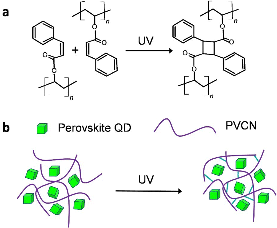 | ||
| Scheme 1 (a) Chemical structure of PVCN and its crosslinking reaction upon UV excitation. (b) Schematic representation of the formation of PeQD–PNCs based on FAPbBr3 QDs and PVCN polymers, before and after UV excitation. | ||
Experimental section
Synthesis of FAPbBr3 QDs
All chemicals were used as received. The FAPbBr3 QDs were synthesized following a ligand-assisted re-precipitation (LARP) method at room temperature;23 post-treatment, including processing with excess PbBr2 and methyl acetate, was applied to improve their light-emitting properties.16,17 Details of the synthesis of the QDs are provided in the ESI.†Fabrication of QD-LEDs
Pictures of the QD-LEDs are provided in Fig. 2a and b. To fabricate an “in-chip” QD-LED,24 the FAPbBr3 QDs were first mixed with the precursors of polydimethylsiloxane (PDMS) (Sylgard™ 184, Dow Corning®). A blue LED in a 5070 package was then filled with this mixture (Fig. 2a) and the whole sample was heated at 100 °C for 1 h (Fig. 2b).Photopatterning processes
PVCN (MW = 40![[thin space (1/6-em)]](https://www.rsc.org/images/entities/char_2009.gif) 000; PDI ≈ 2.5) was purchased from Sigma-Aldrich and used as received. Solutions of PVCN having concentrations from 0.1 to 0.5 wt% were prepared in toluene. A toluene solution of PVCN and the FAPbBr3 QDs (4 to 6 wt%) was spin-coated on a pre-cleaned glass substrate at a spin speed of 900 rounds per minute (rpm) for 30 s and, then, at 1500 rpm for 60 s. The sample was heated at 60 °C for 5 min. A 4 W compact UV lamp was used for large-area photolithography processes. The composite films were exposed to UV light for 10 min; the exposure dose was about 10 J cm−2. Microscale patterning was performed using a double-side mask aligner equipped with a 1000 W UV light (AG1000-4D-D-S-M-V, M&R Nano Technology), the UV exposure time was 8 min, and the dose was about 12 J cm−2. After UV irradiation, the films were developed by dipping the samples in PGMEA for 45 min; PGMEA could remove the unexposed portions. Finally, the samples were annealed at 80 °C for 20 min.
000; PDI ≈ 2.5) was purchased from Sigma-Aldrich and used as received. Solutions of PVCN having concentrations from 0.1 to 0.5 wt% were prepared in toluene. A toluene solution of PVCN and the FAPbBr3 QDs (4 to 6 wt%) was spin-coated on a pre-cleaned glass substrate at a spin speed of 900 rounds per minute (rpm) for 30 s and, then, at 1500 rpm for 60 s. The sample was heated at 60 °C for 5 min. A 4 W compact UV lamp was used for large-area photolithography processes. The composite films were exposed to UV light for 10 min; the exposure dose was about 10 J cm−2. Microscale patterning was performed using a double-side mask aligner equipped with a 1000 W UV light (AG1000-4D-D-S-M-V, M&R Nano Technology), the UV exposure time was 8 min, and the dose was about 12 J cm−2. After UV irradiation, the films were developed by dipping the samples in PGMEA for 45 min; PGMEA could remove the unexposed portions. Finally, the samples were annealed at 80 °C for 20 min.
Material and optical characterization
Transmission electron microscopy (TEM) images were recorded using a field emission gun transmission electron microscope (JEM-2100F, JEOL). The absorption spectra were recorded using a UV/Vis spectrometer (PerkinElmer UV/Vis Lambda 650). The photoluminescence (PL) spectra were recorded using a μPL system equipped with a high-resolution microscope. The time-resolved PL (TRPL) measurements were performed using a 375 nm pulsed laser (PDL200-B); the dynamic signal was recorded using a time-correlated single photon counting spectrometer (LDH-P-C-470, Picoquant). The PL images were recorded using a fluorescence microscope. The absolute PLQYs were measured using an integrating sphere (Isuzu Optic), with a 405 nm laser as the excitation light source.Results and discussion
We synthesized FAPbBr3 QDs through a LARP method at room temperature.16,17,23 The emission properties of the QDs were improved upon post-treatment.17Fig. 1a displays a transmission electron microscopy (TEM) image of the as-prepared QDs, which were typical cubic nano-sized crystals. Fig. S1a (ESI†) shows the size distribution for the sample and the average size was 11 ± 2 nm. The high-resolution TEM (HRTEM) image of the QDs is shown in Fig. S1b (ESI†). We clearly observed the crystalline lattice fringes of these QDs in the HRTEM image. The inset to Fig. S1b (ESI†) displays the corresponding fast Fourier transform (FFT) pattern, which also indicated their high degree of crystallinity. Fig. S1c (ESI†) shows the X-ray diffraction (XRD) pattern of the FAPbBr3 QDs. A series of diffraction peaks at 14.9°, 29.9° and 45.2° were observed, which could be assigned to (100), (200) and (300) planes, respectively.25 The full width at half maximum (FHWM) of the (100) peak was less than 0.4°, revealing the high crystallinity of the QDs.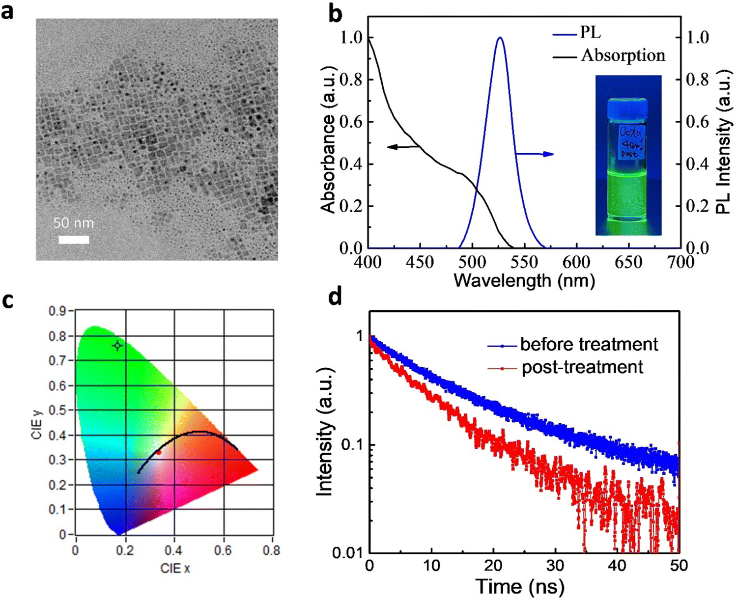 | ||
| Fig. 1 Properties of the FAPbBr3 QDs. (a) The TEM image of the QDs. (b) The absorption and emission spectra of the QDs in toluene; inset: photograph of the FAPbBr3 QDs in a toluene solution under UV excitation. (c) Color coordinates of the green emission from the toluene solution. (d) The TRPL decay curves of the FAPbBr3 QDs in toluene. | ||
Fig. 1b presents the absorption and emission spectra of the FAPbBr3 QDs. The band edge was close to 540 nm, consistent with previous reports.17 The QDs were readily dispersed in toluene, with the solutions exhibiting bright photoluminescence (PL) (inset to Fig. 1b). The PL peak was located at 527 nm with a full width at half maximum (FWHM) of 29 nm. The Commission Internationale de l’Eclairage (CIE) color coordinates of the green emission from the toluene solution (Fig. 1c) were (0.169,0.760), very close to the BT.2020 standard of (0.170, 0.797), suggesting their great potential for use in display applications.26,27 We also used an integrating sphere to measure PLQYs of the QDs. The PLQY of the as-prepared FAPbBr3 QDs in toluene was 80 ± 2%. After post-treatment, the PLQY of the FAPbBr3 QDs increased to 96 ± 2%, with the best PLQY reaching 98%.
We probe the PL properties of the QDs using time-resolved photoluminescence (TRPL) spectroscopy. Fig. 1d displays the TRPL curves of the FAPbBr3 QDs in toluene. They could be fitted to a biexponential decay function, where A and τ are the amplitude components and lifetimes, respectively.26 The fast decay (τ1) was related to the recombination of initially generated excitons upon light absorption; the slower decay (τ2) was associated with exciton recombination with the involvement of surface states.23 The average lifetime (τave) is defined as τave = A1·τ1 + A2·τ2. Fitting the data for the as-prepared QDs (without post-treatment) provided values of τ1 and τ2 of 9.99 ns (relative percentage: 78.6%) and 33.36 ns (21.4%), respectively; τave was 15.00 ns. After post-treatment, the lifetimes became shorter: τ1 and τ2 were 7.86 and 24.42 ns, respectively, giving a value of τave of 9.84 ns. The shorter lifetimes of the QDs prepared with post-treatment indicated faster rates of radiative decay, consistent with the higher PLQYs. Furthermore, the value of A1 increased to 88.1%, suggesting greater importance for the first exciton recombination. The percentage of decay processes involving surface state (A2) decreased because the formation of surface defects was suppressed.23 As a result, post-treatment could effectively decrease the density of defect states.17
Fig. S2 (ESI†) shows the Fourier-transform infrared spectroscopy (FTIR) spectra of the FAPbBr3 QDs prepared before and after post-treatment. A sharp peak at 1710 cm−1 was clearly observed; it can be ascribed to the C![[double bond, length as m-dash]](https://www.rsc.org/images/entities/char_e001.gif) O stretching vibration belonging to the OA molecules.28 The spectrum was almost the same after the post-treatment, suggesting that the chemical bonding was not altered significantly. The result suggests that the improved PLQY was mainly due to the fixing of the surface defects by PbBr2 and reducing aggregation after post-treatment.17
O stretching vibration belonging to the OA molecules.28 The spectrum was almost the same after the post-treatment, suggesting that the chemical bonding was not altered significantly. The result suggests that the improved PLQY was mainly due to the fixing of the surface defects by PbBr2 and reducing aggregation after post-treatment.17
Having obtained highly luminescent FAPbBr3 QDs, we fabricated green LEDs by positioning the PeQDs on blue-emitting GaN chips. Fig. 2a and b display images of a typical “in-chip” QD-LED.21,24 We blended the FAPbBr3 QDs with PDMS and used the resulting mixture to fill in a blue LED. Fig. 2a reveals that the initial QD mixture was yellow-green, but it turned yellowish-brown after heating at 100 °C for 1 h (Fig. 2b), presumably because the QDs underwent some degree of aggregation.29Fig. 2d presents the electroluminescence (EL) spectra of the QD-LED operated with various injection currents. When the current was high (>20 mA), we observed minor blue emission near 448 nm, but green emission, with its peak located at 531 nm, was clearly evident. The spectra clearly indicate that greater than 99% of the photons had been absorbed by the QDs embedded in PDMS. The peak position of the EL emission was slightly red-shifted (by 4 nm), presumably because of some degree of QD aggregation, as noted above. Fig. 2e displays the CIE color coordinates of the blue LED, the green emission of the QD-LED, and the BT.2020 green standard.26,27 The coordinates of the QD-LED were (0.183,0.756) – again, very close to the BT.2020 green standard. The highest power efficiency of the QD-LED was 129.4 lm W−1 (Fig. 2f). The efficiency remained as high as 63.1 lm W−1 when the current was 70 mA, suggesting great practical potential for such QD-LEDs.
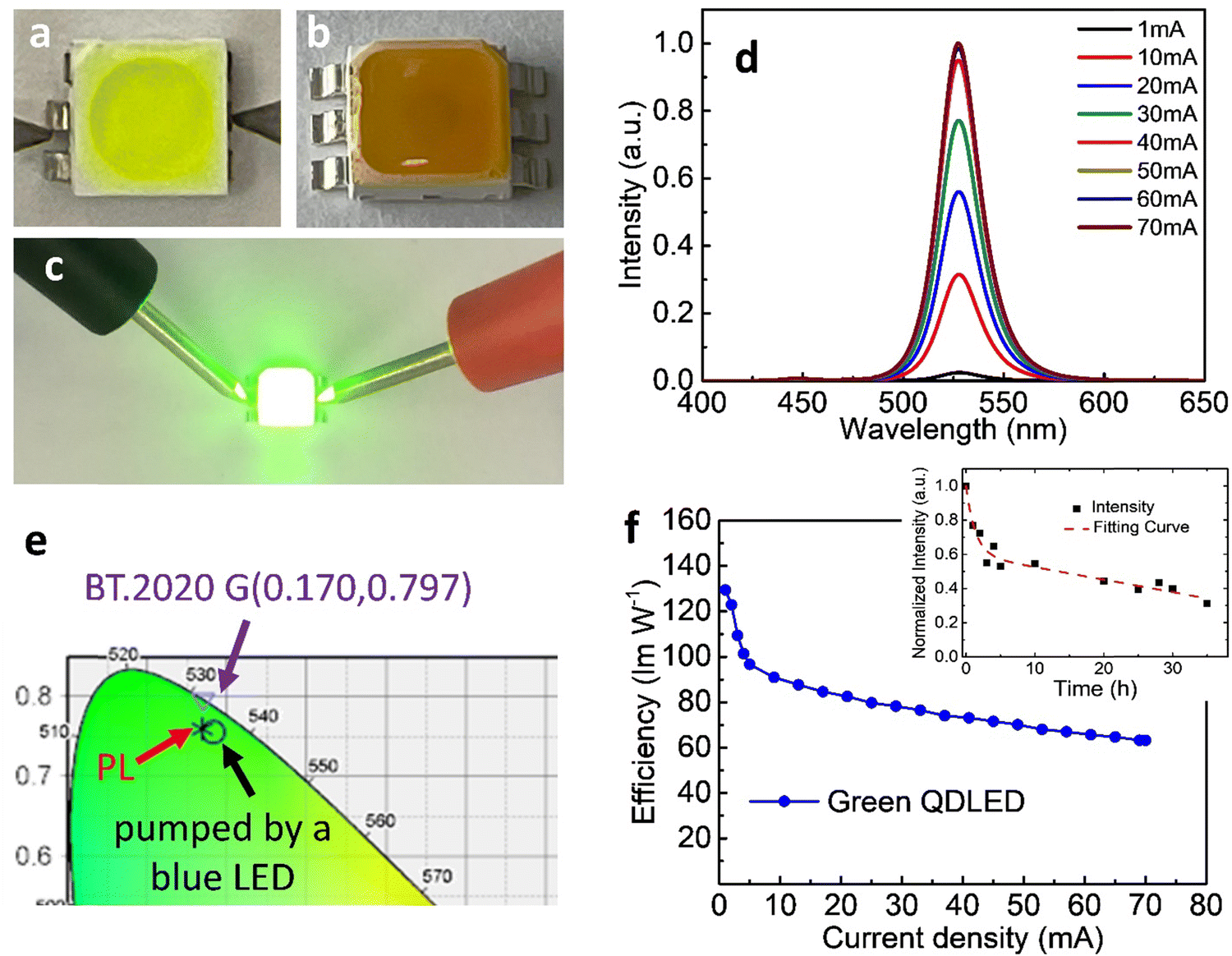 | ||
| Fig. 2 Performance of a green LED prepared using FAPbBr3 QDs. (a) The optical image of the LED filled with a mixture of QDs and PDMS. (b) The optical image of the LED after heating at 100 °C. (c) Optical image of a QD-LED under a bias. (d) Current-dependent spectra of the QD-LED. (e) CIE color coordinates of blue emission from the LED, green emission of the QD-LED, and the BT.2020 green standard. (f) Power efficiency of the LEDs plotted with respect to the current density. The inset shows the time-dependent normalized intensity of the emission from the QD-LED. | ||
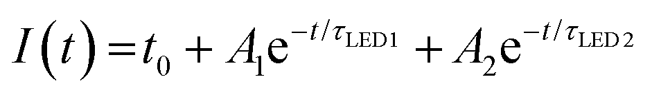
The stability of the QD-LED was further tested and the results are revealed in the inset to Fig. 2f. We found that the normalized intensity (I) as a function of continuous bias stress can be fitted using a biexponential decay eqn (1),
 | (1) |
One of the main hurdles to developing photopatternable PeQDs is their poor resistance against polar solvents. Because of the ionic nature of perovskite materials, they are extremely sensitive to polar solvents.11,12 Accordingly, we intentionally selected cross-linkable PVCN as the host polymer; we expected the crosslinked PVCN to protect the QDs from atmospheric stresses (Scheme 1b). Scheme 1a displays the chemical structure of PVCN and its crosslinking chemical reaction under UV irradiation. To demonstrate the functionality of the PeQD–PNCs, we blended the FAPbBr3 QDs with PVCN at various concentrations, using toluene as the nonpolar solvent. We could obtain patterns of the PeQDs when using well-established procedures for photolithography employed in the semiconductor industry. First, we spin-coated the mixture onto glass substrates and irradiated them with UV light from a 4 W compact UV lamp. We then developed the samples using propylene glycol monomethyl ether acetate (PGMEA).
Fig. S3 (ESI†) shows the PL and absorption spectra of PeQD–PNC films. We can see that the two absorption spectra were very similar to those of the FAPbBr3 QDs (Fig. 1b), suggesting that the chemical structures were not changed. Additionally, because PVCN shows absorption mainly in the UV regime19 and it was buried in the absorption of the glass substrate and QDs, we were not able to detect the chemical reaction of PVCN currently. The PL peak of the PeQD–PNC film was located at 532 nm with an FWHM of 27 nm, suggesting that the emissive properties of the QDs were not affected too much in the PVCN matrix. Fig. 3a presents the patterned logo of our university, prepared on glass substrates; the size of the substrate for each letter was 3 × 3 cm. The patterning processes could also be performed on flexible substrates; Fig. 3b displays a substrate made of PDMS, providing a sample exhibiting great flexibility.
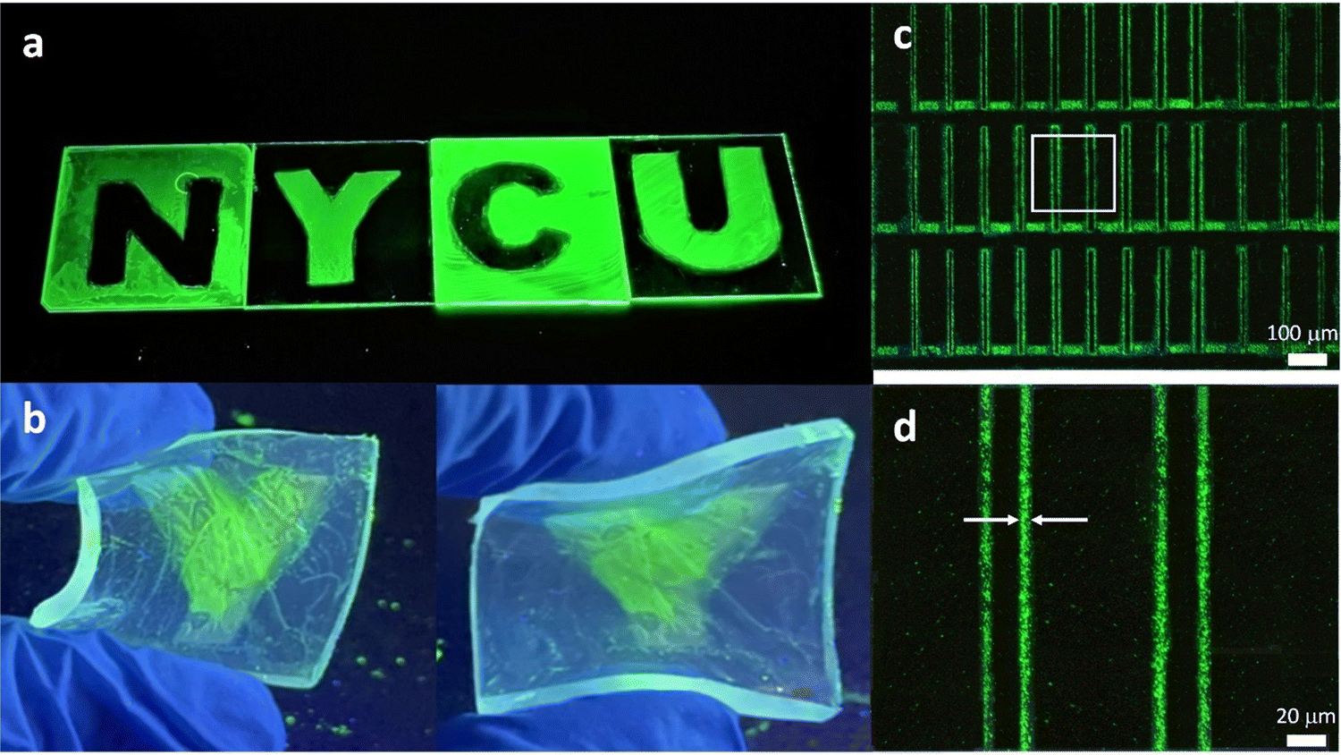 | ||
| Fig. 3 Patterning of PeQD–PNC. (a) Negative patterns of the PeQD–PNC on glass substrates. (b) Pattern on a flexible PDMS substrate. (c) Microscale pattern formed using the PeQD–PNC. (d) Detailed view of the pattern, enlarged from the white square in (c). | ||
Many optoelectronic applications require QD patterns to have small feature sizes;13–15,22 for example, when using PeQDs as CCLs in full-color μ-LED displays.22 To implement microscale patterns, we employed a mask aligner equipped with a 1000 W UV light to perform the patterning process with the PeQD–PNCs. As revealed in Fig. 3c, we could fabricate a repeating line pattern when following the photolithographic protocol described above, confirming the possibility of successful microscale patterning of PeQDs. From the magnified image (Fig. 3d), the line widths were as thin as 3.86 μm. Such a feature size, in theory, would be sufficient for implementation of high-resolution μ-LED displays. From Fig. 3c and d, we can see that the PL uniformity of the pattern was poor. We suspect that a certain level of phase separation still occurred in the patterned films. The surface of the PeQDs could be further modified through exchanging the surface ligands to inhibit phase separation between PeQDs and the host polymer, thereby improving the film quality.
One challenge when using PeQDs is their poor stability against environmental stress. To study the stability of the PeQDs, we prepared neat films of the FAPbBr3 QDs on glass substrates and then stored the samples exposed to the normal atmosphere without any encapsulation. Fig. 4a displays the time-dependent PLQYs of these films. The best PLQY reached as high as 40%, but it decayed very rapidly under the storage conditions; for example, the PLQY became 12% after 48 h. Although thicker films exhibited better stability, their PLQYs also decayed. Fig. 4b displays the results of the stability tests for the PeQD–PNC films. Interestingly, the PLQYs measured immediately after preparation were very low: 10.4, 13.1, and 15.6% for the films prepared with 0.1, 0.2, and 0.5 wt% PVCN solutions. We suspect that the low PLQYs were a consequence of the UV irradiation. The PLQYs were also related to the amounts of PVCN in the PeQD–PNC films, with the initial PLQY increasing upon increasing the concentration of PVCN. We suspect that higher amounts of PVCN absorbed more UV photons, thereby minimizing the exposure of the FAPbBr3 QDs to UV light.
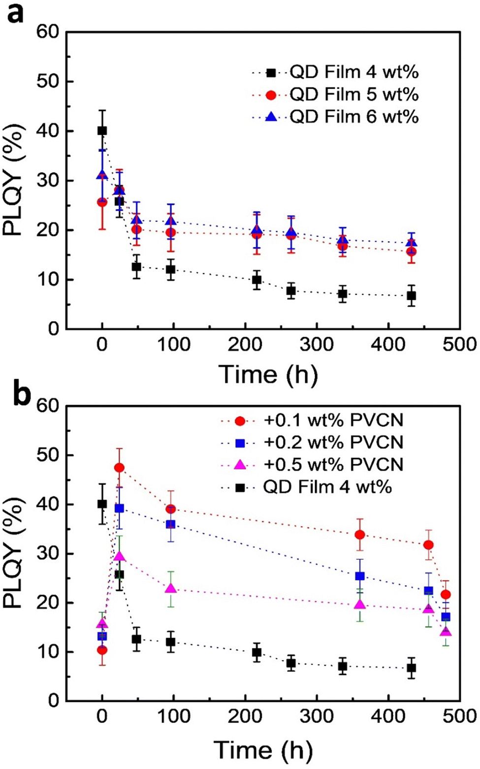 | ||
| Fig. 4 Stability tests of the FAPbBr3 QDs after storage under ambient conditions; the relative humidity was kept at ca. 60%. (a) Time-dependent PLQYs of neat QD films prepared using various concentrations in toluene. (b) Time-dependent PLQYs of the PeQD–PNC films; the PLQYs of a neat QD film (4 wt%) are provided to serve as a benchmark. | ||
Interestingly, the PLQYs recovered significantly after 24 h. When the concentration of PVCN was 0.1 wt%, at which the film exhibited the lowest initial PLQY, the PLQY reached as high as 48% – a value even higher than the best PLQY of the neat films (40%), presumably because of dilution effects, which decreased the reabsorption efficiency. The PLQY of the PeQD–PNC film was also more stable. After 20 days (480 h), the PLQY remained greater than 20% (22%). When compared with the neat film, the PeQD–PNC films were appreciably more stable (Fig. 4b). To understand the reasons behind the improved stability, we measured the contact angles of the neat PeQD and PeQD–PNC films (Fig. S4, ESI†). The water contact angles were 58.8° and 56.6° for the PeQD and PeQD–PNC films, respectively. The comparable water contact angles indicated that they have similar hydrophobicity. Therefore, the presence of the crosslinked PVCN, which was relatively hydrophobic, appeared to slow down the rate of penetration of moisture from the atmosphere, thereby improving the stability of the PeQD–PNC films.
To investigate the PL recovery, we recorded the evolution of the PLQY during the preparation of the PeQD–PNC films (Fig. S5, ESI†). After a typical patterning process, the PLQY was 45% immediately after UV exposure for 10 min. When the exposure time was longer, the PLQY decreased, implying that UV illumination degraded the PL performance. After the wet-etching step, the PLQY decreased dramatically to 18%, indicating that the etching step affected the PL performance significantly. The last processing step, hard baking, slightly decreased the PLQY when the exposure time was 10 min; for other exposure times, the PLQY recovered slightly, suggesting that the heating step was not the major process responsible for decreasing the PL. From these results, we suspect that the wet-etching step probably led to desorption of the surface ligands, with the PL undergoing self-recovery after re-adsorption of the ligands.30 The ligand binding to the surface of the PeQDs is highly dynamic and therefore, ligands are easily lost during the wet processes.30,31 Therefore, the quenching and recovery of the emission could have originated from desorption and re-adsorption of the ligands. More experiments will have to be performed, however, to confirm the details of the mechanism of this PL recovery.
Conclusions
Among the methods for constructing high-performance light-emitting devices using perovskite materials,32–34 PeQDs provide an effective approach because of their high luminescence properties. In this study, we have synthesized highly luminescent PeQDs based on FAPbBr3 for light-emitting applications; the best PLQY of the PeQDs in toluene was 98%. The FAPbBr3 QDs behaved as effective CCLs for LEDs, with greater than 99% of blue photons being converted to green emission. The resulting green QD-LED achieved a high device efficiency of 129.4 lm W−1. Furthermore, when we blended a photopatternable polymer, PVCN, with the FAPbBr3 QDs, we could adopt well-established procedures for photolithography in the semiconductor industry to process our nanocomposites. More importantly, PVCN possesses reasonable solubility in nonpolar solvents (including toluene), thereby avoiding any possible degradation of PeQDs that might have occurred in polar solvents and allowing them to maintain their structural integrity. As a result, we could pattern the PeQD–PNCs using UV light, achieving feature sizes as small as 3.86 μm. Moreover, the PLQY and stability both improved when using the PVCN polymer as the matrix. The adoption of the photopatternable polymer helped us to protect the PeQDs from stresses induced by the atmosphere.The uniformity of the PeQD–PNC films is still not satisfactory; it is probably due to the phase separation between the PeQDs and the host polymer. In the future, we can further modify the surface of the PeQDs through exchanging the surface ligands to inhibit phase separation. The image quality could be improved after we inhibit the phase separation. Overall, this study suggests that PeQD–PNCs have potential for use as color conversion films in high-definition μ-LEDs. We also anticipate that the development of PeQD–PNCs might open up new opportunities for realizing new optoelectronic applications for PeQDs.
Conflicts of interest
There are no conflicts to declare.Acknowledgements
This work is supported by the National Science and Technology Council, Taiwan (grant No. MOST 109-2221-E-009-147-MY3, MOST 111-2218-E-A49-019-MBK, MOST 111-2124-M-A49-004, and MOST 111-2634-F-A49-007) and the Center for Emergent Functional Matter Science of National Yang Ming Chiao Tung University from The Featured Areas Research Center Program within the framework of the Higher Education Sprout Project by the Ministry of Education (MOE) in Taiwan.References
- Y. Bai, M. Hao, S. Ding, P. Chen and L. Wang, Adv. Mater., 2022, 34, 2105958 CrossRef CAS.
- M. Yu, M. H. Saeed, S. Zhang, H. Wei, Y. Gao, C. Zou, L. Zhang and H. Yang, Adv. Funct. Mater., 2022, 32, 2109472 CrossRef CAS.
- S. S. Bhosale, E. Jokar, Y. T. Chiang, C. H. Kuan, K. Khodakarami, Z. Hosseini, F. C. Chen and E. W. G. Diau, ACS Appl. Energy Mater., 2021, 4, 10565–10573 CrossRef CAS.
- T. Chiba and J. Kido, J. Mater. Chem. C, 2018, 6, 11868–11877 RSC.
- Y. F. Li, J. Feng and H. B. Sun, Nanoscale, 2019, 11, 19119–19139 RSC.
- L. Hu, Q. Zhao, S. Huang, J. Zheng, X. Guan, R. Patterson, J. Kim, L. Shi, C. H. Lin, Q. Lei, D. Chu, W. Tao, S. Cheong, R. D. Tilley, A. W. Y. Ho-Baillie, J. M. Luther, J. Yuan and T. Wu, Nat. Commun., 2021, 12, 466 CrossRef CAS PubMed.
- A. Perveen, L. Deng, A. Muravitskaya, D. Yang, A. Movsesyan, S. Gaponenko, S. Chang and H. Zhong, Opt. Mater. Express, 2020, 10, 1659–1671 CrossRef CAS.
- H. C. Yoon, H. Lee, H. Kang, J. H. Oh and Y. R. Do, J. Mater. Chem. C, 2018, 6, 13023–13033 RSC.
- Y. S. Park, S. Guo, N. S. Makarov and V. I. Klimov, ACS Nano, 2015, 9, 10386–10393 CrossRef CAS PubMed.
- F. Hu, H. Zhang, C. Sun, C. Yin, B. Lv, C. Zhang, W. W. Yu, X. Wang, Y. Zhang and M. Xiao, ACS Nano, 2015, 9, 12410–12416 CrossRef CAS.
- Y. Wei, Z. Cheng and J. Lin, Chem. Soc. Rev., 2019, 48, 310–350 RSC.
- Y. Sun, H. Zhang, K. Zhu, W. Ye, L. She, X. Gao, W. Ji and Q. Zeng, RSC Adv., 2021, 11, 27333–27337 RSC.
- J. Yang, D. Hahm, K. Kim, S. Rhee, M. Lee, S. Kim, J. H. Chang, H. W. Park, J. Lim, M. Lee, H. Kim, J. Bang, H. Ahn, J. H. Cho, J. Kwak, B. Kim, C. Lee, W. K. Bae and M. S. Kang, Nat. Commun., 2020, 11, 2874 CrossRef CAS.
- J. Ko, J. H. Chang, B. G. Jeong, H. J. Kim, J. F. Joung, S. Park, D. H. Choi, W. K. Bae and J. Bang, ACS Appl. Mater. Interfaces, 2020, 12, 42153–42160 CrossRef.
- Y. Wang, I. Fedin, H. Zhang and D. V. Talapin, Science, 2017, 357, 385–388 CrossRef CAS PubMed.
- F. D. Stasio, S. Christodoulou, N. Huo and G. Konstantatos, Chem. Mater., 2017, 29, 7663–7667 CrossRef CAS.
- F. D. Stasio, I. Ramiro, Y. Bi, S. Christodoulou, A. Stavrinadis and G. Konstantatos, Chem. Mater., 2018, 30, 6231–6235 CrossRef.
- F. C. Chen, T. D. Chen, B. R. Zeng and Y. W. Chung, Semicond. Sci. Technol., 2011, 26, 034005 CrossRef.
- J. Jang, S. Nam, J. Hwang, J. J. Park, J. Im, C. E. Park and J. M. Kim, J. Mater. Chem., 2012, 22, 1054–1060 RSC.
- Z. Liu, C. H. Lin, B. R. Hyun, C. W. Sher, Z. Lv, B. Luo, F. Jiang, T. Wu, C. H. Ho, H. C. Kuo and J. H. He, Light: Sci. Appl., 2020, 9, 83 CrossRef CAS.
- Y. M. Huang, K. J. Singh, T. H. Hsieh, C. Langpoklakpam, T. Y. Lee, C. C. Lin, Y. Li, F. C. Chen, S. C. Chen, H. C. Kuo and J. H. He, Nanoscale, 2022, 14, 4042–4064 RSC.
- Y. Yin, Z. Hu, M. U. Ali, M. Duan, L. Gao, M. Liu, W. Peng, J. Geng, S. Pan, Y. Wu, J. Hou, J. Fan, D. Li, X. Zhang and H. Meng, Adv. Mater. Technol., 2020, 5, 2000251 CrossRef CAS.
- F. Zhang, H. Zhong, C. Chen, X. Wu, X. Hu, H. Huang, J. Han, B. Zou and Y. Dong, ACS Nano, 2015, 4, 4533–4542 CrossRef.
- S. C. Hsu, Y. M. Huang, C. P. Huang, T. Y. Lee, Y. Y. Cho, Y. H. Liu, A. Manikandan, Y. L. Chueh, T. M. Chen, H. C. Kuo and C. C. Lin, ACS Omega, 2021, 6, 2836–2845 CrossRef CAS PubMed.
- K. Hills-Kimball, Y. Nagaoka, C. Cao, E. Chaykovsky and O. Chen, J. Mater. Chem. C, 2017, 5, 5680–5684 RSC.
- Y. Zu, J. Xi, L. Li, J. Dai, S. Wang, F. Yun, B. Jiao, H. Dong, X. Hou and Z. Wu, ACS Appl. Mater. Interfaces, 2020, 12, 2835–2841 CrossRef PubMed.
- S. W. Dai, Y. L. Lai, L. Yang, Y. T. Chuang, G. H. Tan, S. W. Shen, Y. S. Huang, Y. C. Lo, T. H. Yeh, C. I. Wu, L. J. Chen, M. Y. Lu, K. T. Wong, S. W. Liu and H. W. Lin, ACS Appl. Mater. Interfaces, 2021, 13, 25202–25213 CrossRef CAS PubMed.
- H. Zhao, H. Chen, S. Bai, C. Kuang, X. Luo, P. Teng, C. Yin, P. Zeng, L. Hou, Y. Yang, L. Duan, F. Gao and M. Liu, ACS Energy Lett., 2021, 4, 2395–2403 CrossRef.
- Y. Xin, H. Zhao and J. Zhang, ACS Appl. Mater. Interfaces, 2018, 10, 4971–4980 CrossRef CAS.
- K. Miyashita, K. Kidokoro, Y. Iso and T. Isobe, ACS Appl. Nano Mater., 2021, 4, 12600–12608 CrossRef CAS.
- J. D. Roo, M. Ibáñez, P. Geiregat, G. Nedelcu, W. Walravens, J. Maes, J. C. Martins, I. V. Driessche, M. V. Kovalenko and Z. Hens, ACS Nano, 2016, 10, 2071–2081 CrossRef PubMed.
- L. Liu, Z. Wang, W. Sun, J. Zhang, S. Hu, T. Hayat, A. Alsaedi and Z. Tan, Chem. Commun., 2018, 54, 13283–13286 RSC.
- Z. Wang, Z. Luo, C. Zhao, Q. Guo, Y. Wang, F. Wang, X. Bian, A. Alsaedi, T. Hayat and Z. Tan, J. Phys. Chem. C, 2017, 121, 28132–28138 CrossRef CAS.
- Z. Wang, T. Cheng, F. Wang, S. Dai and Z. Tan, Small, 2016, 4412–4420 CrossRef CAS PubMed.
Footnote |
| † Electronic supplementary information (ESI) available. See DOI: https://doi.org/10.1039/d2tc01832b |
| This journal is © The Royal Society of Chemistry 2022 |