
High performance ferroelectric field-effect transistors for large memory-window, high-reliability, high-speed 3D vertical NAND flash memory†
Giuk
Kim‡
a,
Sangho
Lee‡
a,
Taehyong
Eom
a,
Taeho
Kim
a,
Minhyun
Jung
a,
Hunbeom
Shin
a,
Yeongseok
Jeong
a,
Myounggon
Kang
b and
Sanghun
Jeon
 *a
*a
aSchool of Electrical Engineering, Korea Advanced Institute of Science and Technology (KAIST), 291 Daehak-ro, Yuseong-gu, Daejeon 34141, Korea. E-mail: jeonsh@kaist.ac.kr
bDepartment of Electronics Engineering, Korea National University of Transportation, 50 Daehak-ro, Daesowon-Myeon, Chungju 27469, Korea
First published on 1st June 2022
Abstract
A ferroelectric field-effect transistor (FeFET) has significant potential as a leading contender to replace current NAND flash memory owing to its high operation speed, low power consumption, and highly attractive nonvolatile characteristics originating from its two stable polarization states. However, the representative gate stack of a metal–ferroelectric–insulator–semiconductor (MFIS) has obvious limitations owing to the large voltage drop across the gate insulator, such as charge injection and trapping, low endurance, and a small memory window. Herein, we introduce unique material and structural approaches to address the crucial problems of previous FeFETs. For the material approach, we engineer the grain size by adjusting the Zr content in the HfZrO film and perform a high-pressure annealing process to maximize the tensile strain on the ferroelectric layer during crystallization. We obtain a large memory window (approximately 5 V) for multi-bit operation (eight states), high program/erase speed (<20 ns), and outstanding endurance (>109 cycles) of FeFETs based on the gate stack of a metal–ferroelectric–metal–insulator–semiconductor (MFMIS). For the structural approach, we present a novel 3D vertical MFMIS ferroelectric NAND flash array, wherein the gate stack is designed to induce active switching of the ferroelectric film even with a vertical structure. Finally, the operation scheme of a 3D ferroelectric NAND flash optimized for multi-string operations free from program disturbance is logically probed using technology computer-aided design simulations with a carefully calibrated model. The 3D ferroelectric NAND flash memory can pave the way for next-generation nonvolatile memory devices based on its superior performance.
1. Introduction
Semiconductor devices have been developed to realize low-power, high-integration, and high-speed operation. Like other nanoelectronics, they have been developed using new materials, nanostructures, and integration methods as traditional functional advances.1–5 Flash memory is a representative example of this trend, with massive data storage capacity, high density, and a large memory window (MW), which enables the storage of multiple bits of data per cell. Flash memory devices are widely employed as storage devices for computers, mobile electronic devices and computing-in-memory, and in neuromorphic applications owing to the aforementioned advantages. However, there are some obvious drawbacks that need to be addressed. Because flash memory utilizes electron trapping and tunneling to update the data storage state of a cell, a high operating voltage of approximately 20 V and a slow operating speed of approximately 10−3 s are inevitable. Moreover, because the tunneling of electrons wears out the tunneling oxide during the data update process, flash memory has obvious weaknesses in terms of program/erase cycling endurance, which becomes significant as the number of bits stored in each cell increases. New types of nonvolatile memory (NVM) technologies, such as resistive random access memory (RRAM) and phase change random access memory (PCRAM), are being actively studied to overcome these restrictions. Nonetheless, performance sufficient to replace commercial NAND flash is yet to be achieved.Ferroelectric field-effect transistors (FeFETs) fabricated using hafnia-based ferroelectrics are attracting considerable attention owing to their low operating voltage, excellent data retention, and fast switching speed. They possess intrinsic nonvolatile memory characteristics resulting from two stable polarization states that can be switched by applying an electric field. Additionally, they have the advantage of being compatible with the conventional fabrication process of complementary metal oxide semiconductors. Conformal deposition of the ferroelectric film is possible even on a vertical structure, such as 3D NAND flash memory, through atomic layer deposition. Accordingly, there have been several demonstrations of 3D ferroelectric NAND (FeNAND) flash memory with a ferroelectric thin film added to the gate stack of an existing NAND flash cell.6–9 However, the results of this study revealed a limited memory window of less than 2 V, which is too small for multi-bit operation.
The memory window of FeFETs is proportional to the physical thickness of the ferroelectric film and the value of the coercive field.10,11 Because the value of the coercive field does not vary dramatically and is normally in the range of 1–2 MV cm−1, increasing the thickness of the ferroelectric film is more effective for obtaining large memory windows. However, as the thickness increases, the proportion of non-ferroelectric phases, such as the monoclinic phase, increases and a dramatic degradation of ferroelectricity occurs, thus leading to a failure in achieving the desired memory window. Accordingly, several approaches have been proposed, such as inserting an interfacial layer or using a seed layer,12–15 to mitigate the aforementioned drawbacks. However, these approaches do not achieve an increase in the memory window proportional to the increase in the thickness of the ferroelectric film, nor do they lead to improvements in terms of reliability. Recently, a 4-bit per cell operation showing a large memory window (12 V) was demonstrated using an asymmetric double-gate structure and body effect.16 Despite the limitations of previous studies in terms of the memory window, the endurance still does not exceed 105 cycles. Moreover, owing to its unique operation scheme using the bottom gate, it is challenging to apply a vertical structure, such as a 3D NAND flash.
Here, we demonstrate unique material and structural approaches to address the key issues with previous FeFETs by introducing ferroelectric films with robust ferroelectricity and high reliability, even with a thickness of 30 nm. To ensure strong ferroelectricity, grain size engineering was performed by controlling the zirconium doping concentration of the hafnium zirconium oxide (HfZrO); simultaneously, high-pressure annealing (HPA) was used to enhance the tensile stress across the HfZrO during the crystallization process. The superior performance of a metal–ferroelectric–metal–insulator–semiconductor (MFMIS) FeFET was experimentally demonstrated, which exhibited multi-bit operation (eight states), fast operation speed (<20 ns), and outstanding endurance (>109). As a future 3D nonvolatile memory device, we present a 3D ferroelectric NAND flash array and its optimal operation scheme that can alleviate the intrinsic problem of an increase in the lateral footprint of a planar structure-based MFMIS FeFET.17,18 The proposed operation scheme of 3D ferroelectric NAND flash was proven to be suitable for multi-string operations free from program/erase disturbances, as verified by technology computer-aided design (TCAD) simulations with a carefully calibrated model. We believe that 3D ferroelectric NAND flash memory is a powerful candidate for next-generation nonvolatile memory devices owing to its superior performance.
2. Result and discussion
Compared to ordinary 3D NAND flash, 3D ferroelectric NAND flash is a ferroelectric NVM with a unique concept that has excellent memory performance realized through structural and material strategies. The aim of these strategies is to achieve a more efficient memory state update mechanism, faster operating speed, and higher reliability.The 3D ferroelectric NAND flash cell has an equivalent gate stack of metal–ferroelectric–metal–(gate) insulator–poly silicon (MFMIS), as shown in Fig. 1(a). It should be noted that the cell has a protruding area that increases the area of the gate insulator covered by the floating gate. This concept is similar to that of a previous study on 3D NAND flash, wherein the coupling ratio was enhanced by increasing the effective area of the floating gate to improve the tunneling efficiency.19 Whereas, in our case, the effective area of the gate insulator is larger compared to the area of the ferroelectric film. This structural approach increases the capacitance (CDE) of the gate insulator compared to the capacitance (CFE) of the ferroelectric film, thus facilitating polarization switching corresponding to the updating of the memory states of the cells. The unnecessary voltage drop in the gate insulator owing to the high dielectric constant of the ferroelectric layer can be minimized. The reduced voltage drop across the gate insulator leads to an improvement in endurance by preventing the degradation of the dielectric, such as charge trapping and early breakdown, owing to the electrical stress. Moreover, our unique structure for 3D ferroelectric NAND flash optimized for application to the 3D vertical structure has an additional advantage in terms of device density, considering that the previous MFMIS FeFETs had limitations due to an increase in the lateral dimensions.
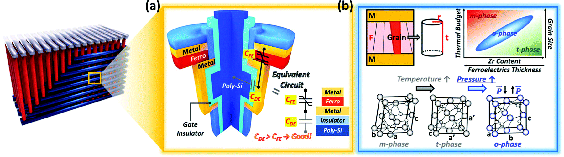 | ||
| Fig. 1 Structural and material approaches for a 3D ferroelectric NAND flash memory device. (a) 3D ferroelectric NAND flash array and highlighted schematic of the 3D MFMIS ferroelectric NAND flash cell as a structural approach. In order to minimize the electrical stress on the gate insulator between the bottom metal and poly Si, the capacitance of the gate insulator (CDE) is designed to have a relatively large value compared to the capacitance of the ferroelectric layer (CFE). The high CDE/CFE can be achieved by maximizing the area of metal-gate insulator-poly Si (MI-poly Si) and minimizing the area between the MFM capacitor and MOSFET. The 3D ferroelectric NAND flash cell shares the equivalent circuit with a planar MFMIS FeFET. (b) Material approach is composed of two processes. The phase engineering with various parameters such as Zr content, ferroelectric thickness, grain size and thermal budget. These parameters are closely correlated with each other and determine a certain phase together. Appropriate grain size can contribute to the formation of a ferroelectric orthorhombic phase (o-phase) in HfZrO. The small grain and large grain are likely to induce a tetragonal phase (t-phase) and a monoclinic phase (m-phase), respectively. | ||
Fig. 1(b) shows the material approach used for the development of a 3D ferroelectric NAND flash. The thickness of the ferroelectric film of the 3D ferroelectric NAND flash was 30 nm to secure a large memory window for multi-state storage per cell. However, in the case of hafnium zirconium oxide (HZO) formed by a typical process, the increase in ferroelectric thickness is accompanied by a larger grain size, thus resulting in the formation of a monoclinic phase (m-phase), which is an obvious obstacle to robust ferroelectricity.20–22 To solve this problem, our approach was used to manipulate the grain size by controlling the doping concentration in ferroelectrics to facilitate the formation of orthorhombic (o-phase) and tetragonal (t-phase) phases. In addition, HPA was utilized for the crystallization of the ferroelectric film to induce larger tensile stress across the ferroelectric film, which led to further formation of the o-phase. The latter sections describe the experimental and simulation validation processes for each approach in detail.
As noted previously, a thick ferroelectric film should be used for large-memory-window FeFETs. However, owing to the unintended dramatic degradation of ferroelectricity above a film thickness of 15 nm, simply increasing the thickness of the ferroelectric film progressively deviates from the theoretical value of the memory window.14 Therefore, we developed a methodology based on the material analysis of the crystal phase and grain size to overcome thickness-related degradation of ferroelectricity.
First, metal–ferroelectric–metal (MFM) capacitors were fabricated to confirm the variation in ferroelectricity with respect to the thickness of the ferroelectric film. For the ferroelectric film, we used Hf0.5Zr0.5Ox with thicknesses of 10, 20, and 30 nm deposited using plasma-enhanced atomic layer deposition. For the metal electrode, TiN with a thickness of 50 nm was deposited by DC sputtering. Rapid thermal annealing (RTA) was conducted at 600 °C for 10 s to crystallize the ferroelectric film immediately after deposition and patterning of the top electrode. Fig. 2(a) shows the polarization–voltage (P–V) curves corresponding to the thickness (10, 20, and 30 nm). It shows a large coercive voltage as the thickness of the ferroelectric film increases, whereas the magnitude of polarization gradually decreases. From the different shapes of the P–V curves, it can be deduced that the ferroelectric films exhibit completely different crystal phases or grain sizes according to the variation in thickness.
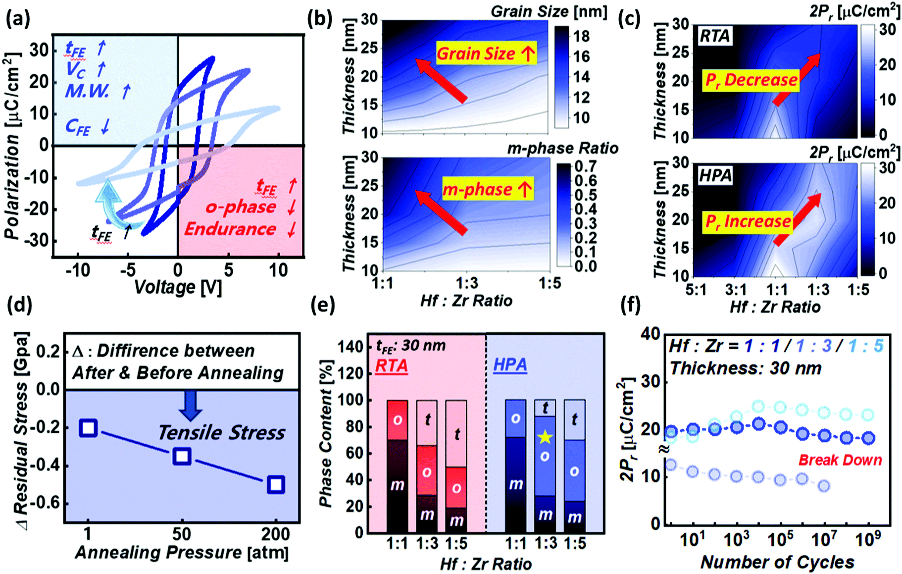 | ||
Fig. 2 Material approaches for high quality ferroelectricity in the relatively thick HfZrO (a) polarization–voltage curves of TiN – 1![[thin space (1/6-em)]](https://www.rsc.org/images/entities/char_2009.gif) :1 HfZrO–TiN capacitor with 10, 20 and 30 nm thick ferroelectric layers. As the thickness of the ferroelectric layer increases, the coercive voltage (VC) increases and CFE decreases, and then this tendency results in the improved memory window (M.W.) property of the FeFET. In contrast, the formation of the o-phase in the relatively thick 1:1 HfZrO film is drastically suppressed. The formation of the m-phase is accelerated, which provokes severe degradation of the endurance property of the ferroelectric layer. (b) The correlation between the normalized grain size extracted from the SEM image and the m-phase portion from the GIXRD data of HfZrO according to various Zr contents and ferroelectric layer thicknesses. The increased grain size provokes m-phase formation. Zr-rich hafnia ferroelectrics have a relatively small grain size, resulting in minimized m-phase formation. (c) Comparison of polarization between HfZrO with various thicknesses and Zr contents annealed by RTA and HPA, respectively. Under the HPA process, ferroelectricity in a relatively thick hafnia is improved compared with that under the RTA process. (d) The variation of residual stress on HfZrO with various annealing pressures. The higher the pressure during the annealing process, the higher the tensile stress on the ferroelectric layer. (e) The phase distribution extracted from the GIXRD data of the 30 nm thick HfZrO with various Zr contents annealed by RTA and HPA, respectively. The maximum o-phase content is observed for a 1:3 HfZrO film under the HPA process, while a relatively small portion of the o-phase is monitored under the RTA process. (f) Endurance characteristics of Zr with varied ferroelectric layers of thickness of 30 nm under the HPA process. Zr-rich ferroelectrics have excellent endurance properties of 1011 cycles, while 1:1 HZO shows limited endurance characteristics of 107 cycles. The amplitude and width of each pulse were determined based on the switching speed of the ferroelectrics. :1 HfZrO–TiN capacitor with 10, 20 and 30 nm thick ferroelectric layers. As the thickness of the ferroelectric layer increases, the coercive voltage (VC) increases and CFE decreases, and then this tendency results in the improved memory window (M.W.) property of the FeFET. In contrast, the formation of the o-phase in the relatively thick 1:1 HfZrO film is drastically suppressed. The formation of the m-phase is accelerated, which provokes severe degradation of the endurance property of the ferroelectric layer. (b) The correlation between the normalized grain size extracted from the SEM image and the m-phase portion from the GIXRD data of HfZrO according to various Zr contents and ferroelectric layer thicknesses. The increased grain size provokes m-phase formation. Zr-rich hafnia ferroelectrics have a relatively small grain size, resulting in minimized m-phase formation. (c) Comparison of polarization between HfZrO with various thicknesses and Zr contents annealed by RTA and HPA, respectively. Under the HPA process, ferroelectricity in a relatively thick hafnia is improved compared with that under the RTA process. (d) The variation of residual stress on HfZrO with various annealing pressures. The higher the pressure during the annealing process, the higher the tensile stress on the ferroelectric layer. (e) The phase distribution extracted from the GIXRD data of the 30 nm thick HfZrO with various Zr contents annealed by RTA and HPA, respectively. The maximum o-phase content is observed for a 1:3 HfZrO film under the HPA process, while a relatively small portion of the o-phase is monitored under the RTA process. (f) Endurance characteristics of Zr with varied ferroelectric layers of thickness of 30 nm under the HPA process. Zr-rich ferroelectrics have excellent endurance properties of 1011 cycles, while 1:1 HZO shows limited endurance characteristics of 107 cycles. The amplitude and width of each pulse were determined based on the switching speed of the ferroelectrics. | ||
Scanning electron microscopy (SEM) and grazing incidence X-ray diffraction (GIXRD) analyses were conducted to investigate the relationship between the thickness of the ferroelectric film and its crystal structure and grain size. For these analyses, MFM capacitors were fabricated by varying the doping concentration and thickness of HfZrO. For the extraction of grain size by SEM analysis, the MFM capacitors were post-metallization-annealed (PMA), and the upper electrodes were removed by wet etching. Fig. S3 (ESI†) shows a plane-view SEM image, where the distributed grains show clear boundaries. Grain size distribution analysis was conducted using the Gwydion software, and the distribution of grain size followed a Gaussian function. In this study, the term “grain size” denotes the median value of each Gaussian distribution.
Fig. 2(b) shows the ratio of the m-phase to the total crystal phase and grain size according to the doping concentration and thickness of the ferroelectric film. For the doping concentration of Hf:Zr = 1:1, the grain size and ratio of the m-phase rapidly increased as the thickness of the ferroelectric film increased. Additionally, the overall dispersion of the grain size increased with the median value, which resulted from the relative decrease in the bulk free energy of the monoclinic phase and its formation is accelerated as the grain size increased.18 The increase in the paraelectric m-phase led to the deterioration of the ferroelectricity, as shown in Fig. 2(a). In contrast, the grain size of the Zr-rich film remained small even with a larger thickness; consequently, the m-phase ratio reduced considerably. Because zirconia has a lower crystallization temperature than hafnia, the Zr-rich ferroelectric film is partially crystallized even during the deposition stage and functions as a uniform crystalline nucleation and growth site during the PMA process. However, compared to the 10 nm-thick ferroelectric film, the Zr-rich ferroelectric film exhibits weak ferroelectricity, which can be attributed to the undesired activation of the tetragonal phase and the antiferroelectric properties. This implies that the tetragonal phase in the Zr-rich film should be converted to the orthorhombic phase, which is directly related to increased ferroelectricity.
We employed HPA to induce substantial tensile stress across the ferroelectric film during the crystallization process, thus facilitating further stabilization of the o-phase.21,23,24Fig. 2(c) shows the 2Pr value extracted from the ferroelectric film crystallized through RTA at 600 °C for 10 s in an N2 ambience and the film subjected to HPA at 450 °C for 30 min in forming gas ambience.
For relatively thick films, the Zr-rich films have greater 2Pr values obtained by HPA than those obtained by RTA. To prove the effect of HPA on the tensile stress inside HfZrO, residual-stress measurements were performed. Fig. 2(d) shows the schematic and results. The value of R (R0) represents the radius of curvature after (before) annealing. From these two values, variation in the residual stress of films with and without annealing can be extracted; a detailed description of the method can be found in a previous report.16 To confirm the effect of high pressure on the tensile stress in the film, ferroelectric films annealed at ambient pressures of 1, 50, and 200 atm were analyzed. The negative value of the difference in residual stress (Δ residual stress) represents tensile stress. From Fig. 2(d), it was observed that strong tensile stress can be applied by using high pressure.
The ratio of the phases in each ferroelectric film obtained through GIXRD analysis is shown in Fig. 2(e). This ratio was obtained by integrating the area of each Gaussian peak, as shown in Fig. S5 (ESI†). Although there was no substantial variation in the ratio of the m-phase for both RTA and HPA, the proportion of the t-phase (o-phase) was diminished (increased) in the case of HPA. Furthermore, this effect was found to be strongest at a Hf:Zr ratio of 1:3, which had the highest o-phase ratio. Fig. S1 (ESI†) shows the polarization–voltage curves with the hafnium/zirconium ratios and thicknesses of the film. In addition, it can be seen that the polarization was most activated at a ratio of 1:3.
Fig. 2(f) shows the endurance of a 30 nm-thick ferroelectric film with respect to the Zr doping ratio when HPA was performed. HfZrO with doping ratios of 1:3 and 1:5 exhibited outstanding endurance characteristics, exceeding 109 cycles. In the case of the 1:5 thin film, the fluctuation of the polarization value according to the operation cycle was severe compared to that for the 1:3 sample. It can be inferred that this occurs from the phase change of the t-phase to the o-phase owing to field cycling.25,26 As such, we developed a ferroelectric film that exhibits robust ferroelectricity and high reliability even at a thickness of 30 nm through Zr doping concentration control and HPA for crystallization, which has high potential as a functional oxide for superior memory applications.
Based on the previously mentioned 30 nm thick ferroelectric film, n-type planar-type MFMIS FeFETs were fabricated. The substrate was p-type silicon, and the gate stack was composed of TiN (approximately 50 nm), HfZrO (Hf:Zr = 1:3; thickness of approximately 30 nm), TiN (approximately 50 nm), SiO2 (approximately 5 nm), and a Si channel. The channel width and length of the MOSFET were fixed at 50 μm and 10 μm, respectively. To control the capacitance ratio between the ferroelectric film and gate insulator, the effective area of the ferroelectric film was modulated while fixing the area of the MOSFET channel; the ratio of the two effective areas was expressed as AFE/AMOS (area of the ferroelectric film divided by the area of the MOSFET's channel). Most of the voltage applied to the gate of the FeFET was delivered to the ferroelectric film through capacitance modulation to induce effective switching operation while alleviating the electrical stress across the gate insulator. Despite the obvious limitation that the MOSFET dimensions should be increased relative to the ferroelectric film, there is a clear advantage regarding memory characteristics and reliability when compared to the existing MFIS FeFET, which suffers from degradation of polarization switching and premature deterioration of the gate insulator owing to the ferroelectric film's high dielectric constant, as shown in Table S4 (ESI†).27–30
Fig. 3(a) shows the capacitance ratio and memory window according to AFE/AMOS. The memory window was extracted from the transfer curve with a voltage sweeping range of ±9 V and shows an increase as the area ratio decreases (the threshold voltage was extracted at a current of 100 nA × W/L = 500 nA). This is due to the above-mentioned effective polarization switching of the ferroelectric film by the modulation of the capacitance ratio. As the memory window is proportional to the thickness of the ferroelectric film, a large memory window of approximately 11 V was observed for an area ratio of AFE/AMOS = 0.026. This large memory window provides sufficient voltage for multi-bit operation, thus increasing the storage density of the device.
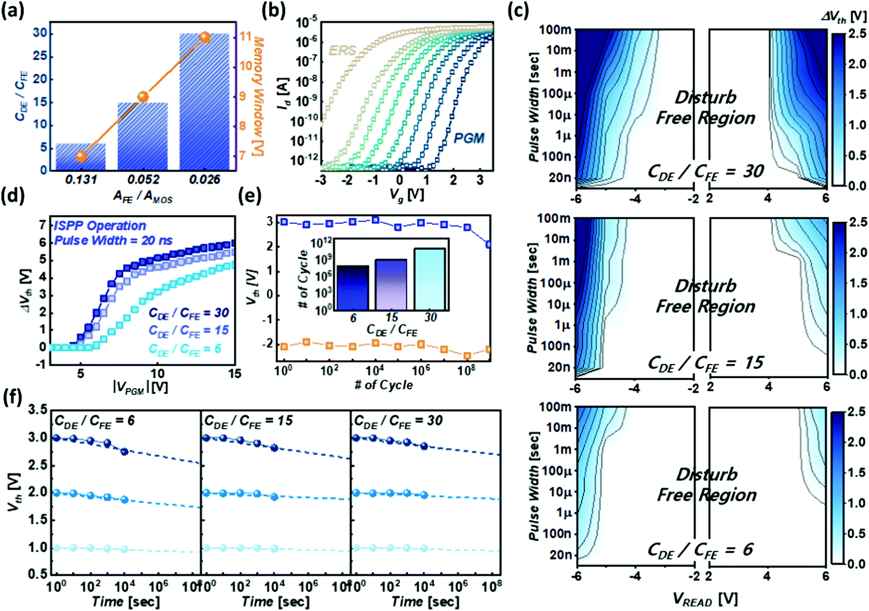 | ||
| Fig. 3 The optimum CDE/CFECFE of the planar MFMIS FeFET for the ferroelectric NAND flash cell (a) CDE/CFE values and memory window extracted from a transfer curve (sweep range = ±10 V) versus AFE/ADE (according to three different AFE/ADE values). The CDE/CFE increases as the AFE/ADE decreases. Then the voltage drop across the ferroelectric layer increases, resulting in the enhanced memory window property of the FeFET. (b) Transfer curve of a 3 bit operation FeFET for CDE/CFE = 15. The FeFETs used in this work have a channel width and length of 50 μm and 10 μm, respectively. The threshold voltages (Vth) are defined as the Vgs yielding Ids = 500 nA (100 nA × W/L). (c) Dependence of pass disturbance on the pulse amplitude and width. As CDE/CFE decreases, the pass disturbance can be suppressed. The disturbance from pass operation stems from the high operation speed of the FeFET because of the shared read and write path in the MFMIS gate stack. (d) Comparison of the ISPP performance of the FeFET for various CDE/CFE values. The program pulse width is 20 ns. The operation speed of the FeFET is improved as CDE/CFE increases. (e) The endurance characteristics of the FeFET for CDE/CFE = 15. The inset shows the number of endurable cycles of the FeFET with various CDE/CFE values. The endurance property of the FeFET is enhanced as CDE/CFE increases. The number of endurable cycles in this work is determined when the memory window of the pristine FeFET decreases by 70% after cycling. (f) Comparison of the retention characteristics of the FeFET for various CDE/CFE values. The depolarization field can be suppressed as CDE/CFE is enhanced. The decreased depolarization field gives rise to the improved retention property of the FeFET. | ||
Although MFMIS FeFETs have the advantage of inducing an effective voltage drop across the ferroelectric film by adjusting the capacitance ratio, they are susceptible to read disturbance because the read voltage can affect the polarization state of the ferroelectric film. Therefore, simply maximizing the capacitance ratio can be detrimental to maintaining a stable memory state. The significance of read disturbance is further emphasized in multi-bit operations because the number of operations for reading the memory state increases in proportion to the number of bits stored in each cell. In this regard, AFE/AMOS = 0.052 (CDE/CFE = 15) may be the optimal ratio for multi-bit operation; to minimize read disturbance, we use the relatively central −3 to 2 V range of the entire memory window for eight memory states targeting the triple-level cell (TLC) operation, as shown in Fig. 3(b). To understand the read disturbance according to the read voltage pulse, the Vth of the FeFET was initially set to a threshold voltage of −3 V and 2 V. The absolute values of the shifted Vth according to the amplitude and width of the applied pulse are expressed as a contour map in Fig. 3(c). The darker blue color indicates the region of a significant shift in threshold voltage, whereas the white color indicates the region of disturbance. As the CDE/CFE value decreased, the disturbance became more severe. In the case of CDE/CFE = 30, a pulse amplitude of 3 V or less was disturbance-free, regardless of the pulse width. The disturbance-free voltage amplitude expanded further to 4 V in the case of CDE/CFE = 15. This means that the eight memory states with a voltage range of –2 to 3 V were in the disturb-free region, and the voltage room for each state was sufficient, even considering the potential polarization disturbance during the read operation. Furthermore, because the threshold voltage value of each memory state was substantially lower than 4 V, it can be inferred that even with repeated read operations, the memory state would be free from potential disturbance. Therefore, when considering the wide memory window and the stability of the stored memory state simultaneously, CDE/CFE = 15 is an optimal option for memory applications.
Fig. 3(d) shows the incremental step programming pulse (ISPP) operation according to various CDE/CFE values, and Fig. S6 (ESI†) shows the switching speed of each FeFET according to the capacitance ratio and Zr doping. The amplitude of the applied pulse was increased while the pulse width was fixed at 20 ns and the initial threshold voltage of the FeFETs was set to −2 V. As the capacitance ratio increased, the ISPP operation exhibited much steeper behavior; i.e., the threshold voltage increased rapidly with the pulse amplitude. For the case of CDE/CFE = 30, it can be confirmed that the change in the threshold voltage at a pulse amplitude of 8 V was approximately 5 V. It should be noted that the required pulse width was drastically reduced considering that the pulse width employed for ISPP operation in a typical 3D NAND flash is in the range of several micro seconds.31 The faster switching operation of our FeFET can lead to a faster update of the memory state, which can improve the speed of overall data processing.
Although high storage capacity can be obtained in 3D NAND flash by using multi-bit operations, the P/E cycling endurance and operation speed diminish as the number of stored bits and required read operations increase. However, our FeFET uses spontaneous polarization rather than a data storage method through a tunneling mechanism. Considering that polarization switching is possible even at a pulse width of 20 ns, endurance can be drastically improved by minimizing electrical stress across the gate stack. Fig. 3(e) shows the endurance of the FeFET with CDE/CFE = 15. The endurable cycle was defined as the point where the memory window decreased by 70% compared to the pristine state. For the FeFET with CDE/CFE = 15, the number of endurable cycles was 109 or more. This is a dramatic improvement over the endurance of FeFETs based on thick ferroelectric films or large memory windows reported so far.11,16,32 The inset in Fig. 3(e) shows the endurance according to the capacitance ratio. It can be seen that the number of endurable cycles increased as the capacitance ratio increased. As the capacitance ratio increased, the state of the FeFET could be sustained for up to about 108 s, or approximately 10 years, as seen in Fig. 3(f), by extrapolating the threshold voltage. This can be explained by the suppression of the depolarization field as the capacitance ratio is increased.
Fig. 4(a) depicts a 3D ferroelectric NAND cell structure that was designed to increase the device density by achieving effective area control between the ferroelectric film and gate insulator in a vertical 3D structure. The area of the gate insulator covered by the lower floating gate was maximized by forming a channel region facing outward from the center of each cell, whereas the overlapping area of the upper and lower floating gates was minimized to reduce the effective area of the ferroelectric film. The value of CDE/CFE in the 3D ferroelectric NAND flash was determined by three main structural parameters as follows: α (the overlapping length between the ferroelectric film and the floating gate); a1 (length from the core to the protrusion of the poly-Si pillar); and h (height of the protrusion of the channel) of the 3D ferroelectric NAND flash.
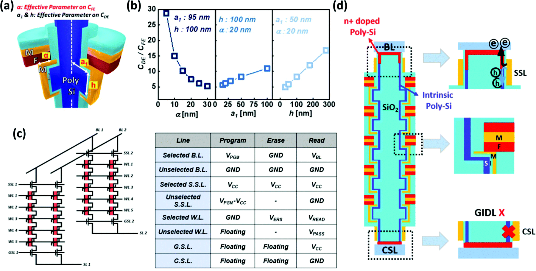 | ||
| Fig. 4 Structural approach for the 3D ferroelectric NAND flash memory device. (a) The structural parameters α (the overlapping length between the ferroelectric film and the floating gate), a1 (length from the core to the protrusion of the poly-Si pillar), and h (height of the protrusion of the channel) of the 3D ferroelectric NAND flash. Each parameter plays a major role in determining the effective area of the ferroelectric layer and the gate insulator. α (a1, h) determines the capacitance of the ferroelectric layer (gate insulator). (b) The analysis of the effect of structural parameters on the capacitance ratio. In order to understand the influence of the individual parameter, the remaining two parameters were fixed. As the overlapping area between the ferroelectric layer (the area of the protrusion) and the floating gate decreases (increases), the capacitance ratio increases. In order to set the optimal capacitance ratio of CDE/CFE in the 3D ferroelectric NAND flash cell, values of α = 12 nm, a1 = 55 nm, and h = 100 nm were used for the future simulation. (c) Scheme for Program, Erase, and read operations. For program operation, VPGM was applied only to the BL of the target string to increase the channel potential by the GIDL phenomenon. (d) Illustration of the GIDL program mechanism. The string select line (SSL) has an overlapped area with a heavily negative doped region that can induce the GIDL phenomenon. The high voltage of the BL contact can be transmitted along the channel due to the generated hole carriers from GIDL. On the ground select line (GSL) side, the GIDL is suppressed since there is no overlap between the gate of the selector transistor and the doped area. | ||
Fig. 4(b) shows the capacitance ratio according to the different values of each structural parameter after fixing the values of the other two parameters. In the cases of a1 and h, the capacitance ratio increased with the increase in these values as they correspond to the diameter and height of the gate insulator. In contrast, a decrease in α, which indicates the overlapping area between the ferroelectric film and floating gate, led to a decrease in the capacitance ratio.
Most studies on vertical FeFETs presented thus far have utilized a negative voltage applied to the gate or word line (WL) to shift the threshold voltage in the negative direction.6,8,33 However, the complexity of the operations increases because additional circuit components are required to use a negative voltage for the data-updating process. This problem can be addressed by referring to the erase operation of the existing 3D NAND flash memory.
The existing 3D NAND flash uses a method of increasing the channel voltage for the erase operation. Gate-induced drain leakage (GIDL)-based erase or bulk erase methods using a common source line (CSL) contact are typical examples wherein hole carriers are injected into the channel to convey high voltage from the CSL contact to the rest of the channel. However, this erase mechanism can also be used for the program operation if the WL of the program target cell is maintained at the ground state while applying a positive voltage to the WLs of the other non-target cells to minimize the voltage difference across the gate stack. However, a simultaneous increase in the channel potential at the strings sharing a CSL makes selective programming of the target cell impossible.
Therefore, we proposed an operation scheme for the selective program operation of 3D ferroelectric NAND flash, as shown in Fig. 4(c). For the program operation of the 3D ferroelectric NAND flash, GIDL was utilized to increase the channel potential. For this, as shown in Fig. 4(d), the heavily doped region was set to overlap the channel of the string select transistor, which was connected to the string select line (SSL). When the program operation proceeded, in the case of a string select transistor, GIDL was induced by applying a low-voltage VCC. At this time, the generated hole carriers were injected into the entire channel and converted into an electrically conducting state. This enabled the high programming voltage of the VPGM applied to the BL to be transmitted through the channel. Conversely, in the case of a non-target string sharing the same SSL with the target string, the BL voltage was set to the ground state, thus avoiding an unnecessary increase in the potential of the channel, while the relatively high voltage of VPGM − VCC was applied to the SSL of the non-target string sharing the same BL to block the GIDL. Through this operational scheme, the channel potential of only the desired string could be selectively increased.
In the case of the target string, the polarization switching of the ferroelectric film leading to a positive shift in the threshold voltage was induced by increasing the channel potential and simultaneously setting the WL of the program target cell to the ground state. This had the equivalent effect of applying a negative voltage to the WL of a programming cell. The WLs of the non-target cells in the same string were floated during the program operation to prevent program disturbances in the string that shares the same WL for which the potential of the channel is not boosted. When the WL was floated, the potential of the entire cell could be boosted owing to the high potential of the channel, thus preventing a voltage difference across the gate stack of the non-target cells. In the case of the erase operation, block erase was performed by applying the erase voltage VERS to all WLs. For the read operation, a pass voltage that can minimize the disturbance in the polarization state of each 3D ferroelectric NAND cell was applied to the target string to extract the current value. The value of the pass voltage corresponded to the read disturbance-free voltage, which was examined earlier.
Fig. 5 shows the results of the TCAD simulation to verify whether the operation scheme of the previously proposed 3D ferroelectric NAND flash is valid. For simplicity, a simulation was performed on a string consisting of five cells, and the detailed methodology of the simulation is explained in the ESI.†
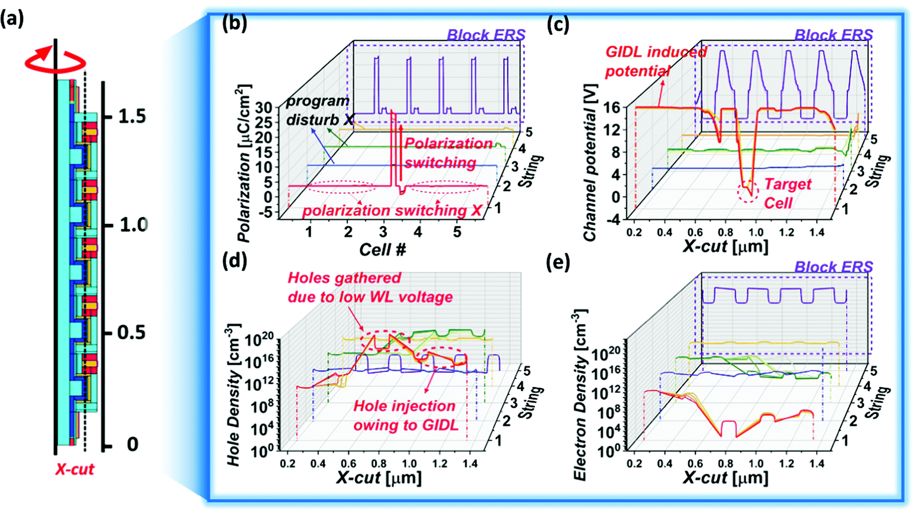 | ||
| Fig. 5 Verification of 3D ferroelectric NAND flash operation. (a) Illustration for the extraction of the electrical values from the X-cut line crossing the ferroelectric film and the channel region of the 3D ferroelectric NAND flash string. (b)–(e) Various electrical changes in the four operation-related strings during the target program of the 3D ferroelectric NAND flash (string 1)/block erase operation. Values were extracted from the channel area covered by the floating gate along the X-cut line. (b) Changes in polarization during the program (represented by strings 1, 2, 3 and 4) and block erase (represented in All) operations. The polarization value of the target cell (between the X-cut value of 0.8 μm and 1.0 μm) reaches about 25 μC cm−2 while there is virtually no change in other cells. This means that a selective program occurs only in the desired string without any program disturbance in other strings or cells. Block erase also operates normally for all strings and cells. The polarization value was presented in absolute values. (c) Electrostatic potential of the strings during program and block erase operations. The voltage drop only occurs at the target cell. All the other cells are in a floating state during the program operation, and then there was no voltage drop across the gate stack. (d) Hole density of the strings during program and block erase operations. Hole carriers supplied by the GIDL at the SSL region are gathered at the target cell due to the relatively low potential applied to the gate at the target cell. (e) Electron density of the strings during program and block erase operations. Electrons gather due to the positive voltage applied to the gate of all cells during block erase operation. | ||
Considering that the four strings are directly involved in the operation of the 3D ferroelectric NAND flash, string 1 was set as the program target string, sharing the WLs with string 2. String 3 shared the BL with string 1, and string 4 was connected to string 3 with the same WLs. During the program operation, cell 3 (connected to WL3) of string 1 was set as the target cell. For the programming operation, the voltage of the BL was maintained at 15 V; the selector transistor was maintained at 2 V; the WL of the target cell was kept in the ground state; and the remaining cells were floated following the aforementioned operation scheme of the 3D ferroelectric NAND flash.
Data along the X-cut line passing through the ferroelectric film and channel region were extracted for the analysis of the electrical values from the 3D ferroelectric NAND flash, as shown in Fig. 5(a). Fig. 5(b)–(e) depict the change in the polarization of each cell, channel potential, hole density, and electron density in the four strings during the program/erase operation, respectively. For the corresponding values, in the case of block erase, because all strings show the same operation, they are marked as “All” in the graph.
Fig. 5(b) shows the polarization value of each string during the program operation. The polarization value of the target cell (between the X-cut value of 0.8 μm and 1.0 μm) reaches approximately 25 μC cm−2, whereas there is virtually no change in other cells. This indicates that selective programming of the target cell was possible while there was no program disturbance (unwanted polarization switching) in other strings or cells. Block erase was found to operate normally for all strings and cells and exhibited a polarization value of –23 μC cm−2. For convenience, the absolute value of polarization is depicted in the figure.
Fig. 5(c) shows the electrostatic potential during the program and block erase operations. Potential boosting owing to GIDL can be seen throughout string 1, where the program target cell is located. The potential profile of string 1 shows two apparent voltage-drop points. The right side is due to the application of the ground voltage to the WL of the target cell, whereas the left side is due to a voltage drop at the buffer oxide caused by the comparatively low voltage of the target cell floating gate. Voltage drop at the buffer oxide, as shown in Fig. 5(b), did not affect the polarization state of the neighboring cell. In the case of neighboring cells, it can be confirmed that there was no potential drop across the cell because the WLs float. The other strings did not have any potential drop across the gate stack because the channel potential was not boosted owing to our program scheme. In contrast, when VERS was applied to each WL during a block erase operation, potential peaks were apparent in each cell.
Fig. 5(d) shows the hole density of the strings during the program and block erase operations. The hole carriers supplied by the GIDL in the SSL region were collected at the target cell owing to the relatively low potential applied to the gate at the target cell. Fig. 5(e) shows the electron density of the strings during the program and block erase operations. Electrons gathered owing to the positive voltage applied to the gate of all cells during the block erase operation.
Fig. 6 shows the electric field profile in the ferroelectric film and gate insulator during the operation of the 3D ferroelectric NAND cell according to the value of α (6, 12, and 30 nm) during the program operation. The closer the displayed color is to red (blue), the stronger (weaker) the electric field intensity. A decrease in α led to a weaker electric field through the gate insulator, which mitigated electrical stress on the gate insulator. For the case of CDE/CFE = 15, the electric field applied to the ferroelectric film (gate insulator) was 3.4 MV cm−1 (4.2 MV cm−1).
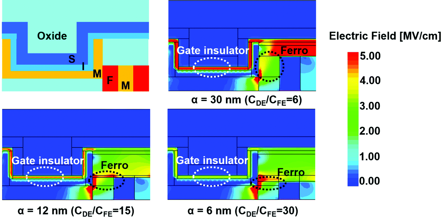 | ||
| Fig. 6 Electric field profile of the 3D ferroelectric NAND flash cell during the program operation. The electric field profile of the 3D ferroelectric NAND flash cell according to the α value (6, 12, 30 nm) during the program operation. The closer the color is displayed to red (blue), the stronger (weaker) the electric field intensity is. A decrease of α leads to a weaker electric field across the gate insulator meaning reduced electrical stress on the gate insulator. | ||
3. Conclusions
We demonstrate a high-performance HfZrO-based FeFET with unique strategies for 3D integration to overcome the limitations of existing ferroelectric memory devices. FeFETs with a wide memory window exceeding 5 V, multi-bit operation with eight memory states, high-speed operation over 20 ns, and high endurance of more than 109 cycles were fabricated using material engineering techniques such as HfZrO doping concentration control and high-pressure annealing. We also propose that the MFMIS FeFET device density problem could be addressed using a structural approach, that is, a 3D ferroelectric NAND flash. The operation scheme was also optimized for the 3D ferroelectric NAND flash structure, and normal program/erase operation was verified through TCAD simulation. Table S3 (ESI†) compares the performance parameters of the 3D ferroelectric NAND flash with those of commercial memory devices. In summary, we present a 3D ferroelectric NAND flash memory with a wide MW, even at a lower operation voltage, enhanced program/erase speed, and higher endurance cycles compared to conventional 3D NAND flash memory based on a HfZrO film that shows excellent ferroelectricity even at a thickness of 30 nm. As a result, the proposed 3D ferroelectric NAND flash, with its superior performance and high density, could be a promising contender for future nonvolatile memory devices and computing-in-memory applications.Data availability
The data that support the findings of this study are available from the corresponding author upon reasonable request.Conflicts of interest
There are no conflicts to declare.Acknowledgements
This work was supported by Grant Nos. NRF-2020M3F3A2A02082436, NRF-2020M3F3A2A01081916, and in part by the IC Design Education Center (IDEC) at EDA tool.References
- J. H. Park, J. H. Shin, J. M. Ju, J. H. Lee, C. Choi, Y. So, H. Lee and J. H. Kim, Modulating the electrocatalytic activity of N-doped carbon frameworks via coupling with dual metals for Zn–air batteries, Nano Convergence, 2022, 9(1), 1–10 CrossRef PubMed.
- C. D. Powell, A. W. Lounsbury, Z. S. Fishman, C. L. Coonrod, M. J. Gallagher, D. Villagran, J. B. Zimmerman, L. D. Pfefferle and M. S. Wong, Nano-structural effects on Hematite (α-Fe2O3) nanoparticle radiofrequency heating, Nano Convergence, 2021, 8(1), 1–9 CrossRef PubMed.
- W. Sohn, K. C. Kwon, J. M. Suh, T. H. Lee, K. C. Roh and H. W. Jang, Microscopic evidence of strong interactions between chemical vapor deposited 2D MoS2 film and SiO2 growth template, Nano Convergence, 2021, 8(1), 1–10 CrossRef PubMed.
- H. K. Choi, C. H. Kim, S. N. Lee, T. H. Kim and B. K. Oh, Nano-sized graphene oxide coated nanopillars on microgroove polymer arrays that enhance skeletal muscle cell differentiation, Nano Convergence, 2021, 8(1), 1–11 CrossRef PubMed.
- W. Sohn, K. C. Kwon, J. M. Suh, T. H. Lee, K. C. Roh and H. W. Jang, Microscopic evidence of strong interactions between chemical vapor deposited 2D MoS2 film and SiO2 growth template, Nano Convergence, 2021, 8(1), 1–10 CrossRef PubMed.
- K. Florent, M. Pesic, A. Subirats, K. Banerjee, S. Lavizzari, A. Arreghini, L. Di Piazza, G. Potoms, F. Sebaai and S. McMitchell, Vertical ferroelectric HfO 2 FET based on 3-D NAND architecture: Towards dense low-power memory, IEEE International Electron Devices Meeting (IEDM), IEEE, 2018, pp. 2.5. 1–2.5. 4 Search PubMed.
- K. Florent, S. Lavizzari, L. Di Piazza, M. Popovici, E. Vecchio, G. Potoms, G. Groeseneken and J. Van IHoudt, First demonstration of vertically stacked ferroelectric Al doped HfO 2 devices for NAND applications, Symposium on VLSI Technology, IEEE, 2017, pp. T158–T159 Search PubMed.
- M.-K. Kim, I.-J. Kim and J.-S. Lee, CMOS-compatible ferroelectric NAND flash memory for high-density, low-power, and high-speed three-dimensional memory, Sci. Adv., 2021, 7(3), eabe1341 CrossRef CAS PubMed.
- K. Banerjee, L. Breuil, A. Milenin, M. Pak, J. Stiers, S. McMitchell, L. Di Piazza and J. van Houdt, First demonstration of ferroelectric Si:HfO2 based 3D FE-FET with trench architecture for dense nonvolatile memory application, IEEE International Memory Workshop (IMW), IEEE, 2021, pp. 1–4 Search PubMed.
- H.-T. Lue, C.-J. Wu and T.-Y. Tseng, Device modeling of ferroelectric memory field-effect transistor (FeMFET), IEEE Trans. Electron Devices, 2002, 49(10), 1790–1798 CrossRef.
- T. Ali, P. Polakowski, K. Kühnel, M. Czernohorsky, T. Kämpfe, M. Rudolph, B. Pätzold, D. Lehninger, F. Müller and R. Olivo, A multilevel FeFET memory device based on laminated HSO and HZO ferroelectric layers for high-density storage, IEEE International Electron Devices Meeting (IEDM), IEEE, 2019, pp. 28.27. 21–28.27. 24 Search PubMed.
- T. Ali, P. Polakowski, S. Riedel, T. Büttner, T. Kämpfe, M. Rudolph, B. Pätzold, K. Seidel, D. Löhr and R. Hoffmann, Silicon doped hafnium oxide (HSO) and hafnium zirconium oxide (HZO) based FeFET: A material relation to device physics, Appl. Phys. Lett., 2018, 112(22), 222903 CrossRef.
- H. Mulaosmanovic, E. T. Breyer, T. Mikolajick and S. Slesazeck, Ferroelectric FETs with 20-nm-thick HfO 2 layer for large memory window and high performance, IEEE Trans. Electron Devices, 2019, 66(9), 3828–3833 CAS.
- M. Hyuk Park, H. Joon Kim, Y. Jin Kim, W. Lee, T. Moon and C. Seong Hwang, Evolution of phases and ferroelectric properties of thin Hf0. 5Zr0. 5O2 films according to the thickness and annealing temperature, Appl. Phys. Lett., 2013, 102(24), 242905 CrossRef.
- W. Xiao, C. Liu, Y. Peng, S. Zheng, Q. Feng, C. Zhang, J. Zhang, Y. Hao, M. Liao and Y. Zhou, Memory window and endurance improvement of Hf0.5 Zr0.5 O2-based FeFETs with ZrO2 seed layers characterized by fast voltage pulse measurements, Nanoscale Res. Lett., 2019, 14(1), 1–7 CrossRef CAS PubMed.
- H. Mulaosmanovic, D. Kleimaier, S. Dünkel, S. Beyer, T. Mikolajick and S. Slesazeck, Ferroelectric transistors with asymmetric double gate for memory window exceeding 12 V and disturb-free read, Nanoscale, 2021, 13(38), 16258–16266 RSC.
- S. Lee, G. Kim, T. Kim, T. Eom and S. Jeon, Vertical Pillar Ferroelectric Field-Effect-Transistor Memory, Phys. Status Solidi RRL, 2021, 2100532 CrossRef.
- J. Sun, Y. Li, L. Cao, J. Liu, X. Shi and L. Tian, Effects of area ratio on the characteristics of metal-ferroelectric-metal-insulator-semiconductor field-effect-transistors (MFMIS FETs), Integr. Ferroelectr., 2019, 201(1), 183–191 CrossRef CAS.
- S. Whang, K. Lee, D. Shin, B. Kim, M. Kim, J. Bin, J. Han, S. Kim, B. Lee and Y. Jung, Novel 3-dimensional dual control-gate with surrounding floating-gate (DC-SF) NAND flash cell for 1Tb file storage application, International Electron Devices Meeting, IEEE, 2010, pp 29.27. 21–29.27. 24 Search PubMed.
- M. H. Park, Y. H. Lee, H. J. Kim, T. Schenk, W. Lee, K. Do Kim, F. P. Fengler, T. Mikolajick, U. Schroeder and C. S. Hwang, Surface and grain boundary energy as the key enabler of ferroelectricity in nanoscale hafnia-zirconia: a comparison of model and experiment, Nanoscale, 2017, 9(28), 9973–9986 RSC.
- Y. Lee, Y. Goh, J. Hwang, D. Das and S. Jeon, The influence of top and bottom metal electrodes on ferroelectricity of hafnia, IEEE Trans. Electron Devices, 2021, 68(2), 523–528 CAS.
- D. Lehninger, R. Olivo, T. Ali, M. Lederer, T. Kämpfe, C. Mart, K. Biedermann, K. Kühnel, L. Roy and M. Kalkani, Back-End-of-Line Compatible Low-Temperature Furnace Anneal for Ferroelectric Hafnium Zirconium Oxide Formation, Phys. Status Solidi A, 2020, 217(8), 1900840 CrossRef CAS.
- Y. Cai, Q. Zhang, Z. Zhang, G. Xu, Z. Wu, J. Gu, J. Li, J. Xiang and H. Yin, Influence of Applied Stress on the Ferroelectricity of Thin Zr-Doped HfO2 Films, Appl. Sci., 2021, 11(9), 4295 CrossRef CAS.
- B. Buyantogtokh, V. Gaddam and S. Jeon, Effect of high pressure anneal on switching dynamics of ferroelectric hafnium zirconium oxide capacitors, J. Appl. Phys., 2021, 129(24), 244106 CrossRef CAS.
- M. H. Park, H. J. Kim, Y. J. Kim, Y. H. Lee, T. Moon, K. D. Kim, S. D. Hyun, F. Fengler, U. Schroeder and C. S. Hwang, Effect of Zr Content on the Wake-Up Effect in Hf1−x ZrxO2 Films, ACS Appl. Mater. Interfaces, 2016, 8(24), 15466–15475 CrossRef CAS PubMed.
- M. Lederer, S. Abdulazhanov, R. Olivo, D. Lehninger, T. Kämpfe, K. Seidel and L. M. Eng, Electric field-induced crystallization of ferroelectric hafnium zirconium oxide, Sci. Rep., 2021, 11(1), 1–7 CrossRef PubMed.
- T. Ali, P. Polakowski, S. Riedel, T. Büttner, T. Kämpfe, M. Rudolph, B. Pätzold, K. Seidel, D. Löhr and R. Hoffmann, High endurance ferroelectric hafnium oxide-based FeFET memory without retention penalty, IEEE Trans. Electron Devices, 2018, 65(9), 3769–3774 CAS.
- J. Duan, H. Xu, S. Zhao, F. Tian, J. Xiang, K. Han, T. Li, X. Wang, W. Wang and T. Ye, Impact of mobility degradation on endurance fatigue of FeFET with TiN/Hf0.5Zr0.5O2/SiOx/Si (MFIS) gate structure, J. Appl. Phys., 2022, 131(13), 134102 CrossRef CAS.
- W. Xiao, C. Liu, Y. Peng, S. Zheng, Q. Feng, C. Zhang, J. Zhang, Y. Hao, M. Liao and Y. Zhou, Performance improvement of Hf 0.5 Zr 0.5 O 2-based ferroelectric-field-effect transistors with ZrO 2 seed layers, IEEE Electron Device Lett., 2019, 40(5), 714–717 CAS.
- S. Zhao, F. Tian, H. Xu, J. Xiang, T. Li, J. Chai, J. Duan, K. Han, X. Wang and W. Wang, Experimental Extraction and Simulation of Charge Trapping During Endurance of FeFET With TiN/HfZrO/SiO2/Si (MFIS) Gate Structure, IEEE Trans. Electron Devices, 2022 DOI:10.1109/TED.2021.3139285.
- H.-T. Lue, T.-H. Hsu, S.-Y. Wang, E.-K. Lai, K.-Y. Hsieh, R. Liu and C.-Y. Lu, Study of incremental step pulse programming (ISPP) and STI edge effect of BE-SONOS NAND flash, IEEE International Reliability Physics Symposium, IEEE, 2008, pp. 693–694 Search PubMed.
- C.-Y. Liao, K.-Y. Hsiang, F.-C. Hsieh, S.-H. Chiang, S.-H. Chang, J.-H. Liu, C.-F. Lou, C.-Y. Lin, T.-C. Chen and C.-S. Chang, Multibit Ferroelectric FET Based on Nonidentical Double HfZrO2 for High-Density Nonvolatile Memory, IEEE Electron Device Lett., 2021, 42(4), 617–620 CAS.
- P. Wang, W. Shim, Z. Wang, J. Hur, S. Datta, A. I. Khan and S. Yu, Drain-erase scheme in ferroelectric field effect transistor—Part II: 3-D-NAND architecture for in-memory computing, IEEE Trans. Electron Devices, 2020, 67(3), 962–967 CAS.
Footnotes |
| † Electronic supplementary information (ESI) available: Polarization–electric field curves for various Hf:Zr ratios and thicknesses, capacitance–voltage curves of HfZrO with a thickness of 30 nm, grain size analysis data (SEM) and extracted grain size distributions, and simulation/fabrication/electrical characterization methods. See DOI: https://doi.org/10.1039/d2tc01608g |
| ‡ These authors contributed equally. |
| This journal is © The Royal Society of Chemistry 2022 |