
2D semiconductor SnP2S6 as a new dielectric material for 2D electronics†
Jiayi
Hu‡
 ab,
Anqi
Zheng‡
b,
Er
Pan
b,
Jiangang
Chen
b,
Renji
Bian
b,
Jinyao
Li
c,
Qing
Liu
*b,
Guiming
Cao
*b,
Peng
Meng
b,
Xian
Jian
ac,
Alexander
Molnar
d,
Yulian
Vysochanskii
*d and
Fucai
Liu
*ab
ab,
Anqi
Zheng‡
b,
Er
Pan
b,
Jiangang
Chen
b,
Renji
Bian
b,
Jinyao
Li
c,
Qing
Liu
*b,
Guiming
Cao
*b,
Peng
Meng
b,
Xian
Jian
ac,
Alexander
Molnar
d,
Yulian
Vysochanskii
*d and
Fucai
Liu
*ab
aYangtze Delta Region Institute (Huzhou), University of Electronic Science and Technology of China, Huzhou, 313099, China. E-mail: fucailiu@uestc.edu.cn
bSchool of Optoelectronic Science and Engineering, University of Electronic Science and Technology of China, Chengdu, 611731, China. E-mail: liuqing19@uestc.edu.cn; guimingcao@163.com
cSchool of Materials and Energy, University of Electronic Science and Technology of China, Chengdu, 611731, China
dInstitute for Solid State Physics and Chemistry, Uzhhorod University, Uzhhorod, Ukraine
First published on 8th July 2022
Abstract
Due to the intriguing optical and electronic properties, 2D materials are promising for next generation optoelectronic and electric device applications. Exploring new 2D materials with novel physical properties is rewarding for this area. In this work, we systematically investigated the optoelectronic properties of 2D metal thiophosphate SnP2S6 with a unique nanoporous structure. The intermediate bandgap makes SnP2S6 a good candidate for both the channel and gate dielectric materials in the transistor device. SnP2S6 showed good photoresponse properties. In addition, the MoS2 transistor with SnP2S6 as a dielectric layer showed a high dielectric constant (≈23) and a low subthreshold slope down to 69.4 mV dec−1, and it presented 0.1 pA scale leakage current, a threshold voltage as low as 1.1 V, an ON/OFF ratio reaching 107 and negligible hysteresis with high stability and reproducibility. This work could open up new avenues for the discovery of new metal thiophosphate systems for future device applications.
 Fucai Liu | Dr Fucai Liu is a full professor at the University of Electronic Science and Technology China. He received his PhD degree and BSc degree from Nankai University China. After graduation, he worked as a postdoc at Tohoku University Japan, and Nanyang Technological University Singapore. His research interests focus on the study of electronic and optoelectronic properties of novel low-dimensional systems and their application in high performance information functional devices. |
Introduction
The emergence of two-dimensional materials has brought new opportunities to the scientific and industrial fields. The quantum confinement effect in the thickness direction of two-dimensional materials is prominent, demonstrating the advantages of high carrier mobility, channel regulation capability and rich properties in force, heat, sound, light, electricity and magnetism.1–4 As a result, novel electronic and optoelectronic devices based on 2D materials are developed and studied, and this is still an active research field today.5–7 The rapid development of 2D materials is beneficial for the discovery of novel 2D materials with exotic physical properties. For example, the discovery of 2D CuInP2S6 brings 2D ferroelectricity and the related device application to the center of the ferroelectric transistor and memory device field. The isolation of layered CrI3 enables truly 2D ferromagnetic properties, attracting a lot of attention in the study of 2D magnetism. Layered ternary compounds such as Ta2PdS6,8 In2P3S9,9 and Bi2O2Se10,11 also provide new opportunities for the electronic and optoelectronic performance improvement for 2D material applications. There exist huge potential, opportunities and challenges for exploring new 2D material systems for application in future nanoelectronics and optoelectronics.12,13For dielectric applications, SiO2 is used as a dielectric layer typically, but traditional silicon-based field effect transistors (FETs) face various challenges when the device scales down to nanometer regime, the most prominent ones of which are reduced mobility and increased short-channel effects.14 In order to mitigate these problems, novel dielectrics with remarkable properties have begun to appear. Advanced functional materials based on eco-friendly cellulose and sputtered multicomponent dielectrics can be processed at low temperatures, and were reported to be implemented as high-capacitance gate dielectrics, bringing new insights into flexible and low-cost transistors and the need to meet the constraints for better band-offset matching.15,16 Moreover, 2D insulators are regarded as the ultimate solution for dielectric miniaturization.17 Hexagonal boron nitride (h-BN) has been deemed as the most promising 2D vdW dielectric layer, while novel 2D materials suitable for using as dielectric layers are rarely reported. However, the low dielectric constant (≈5.0) and excessive leakage current make h-BN unsuitable for ultrascaled FETs with low power consumption.18,19 Therefore, it is important to find new materials to serve as reliable gate dielectrics in FETs.
Among the various 2D material systems, the novel 2D metal thiophosphate MP2X6 (M = metal, X = S or Se)20 has received much attention due to its exceptional physical properties, including magnetic, electronic, ferroelectric, and optical characteristics.21–23 Among the most extensively studied systems is the Sn2P2S6 crystal with a considerable piezo effect, appropriate ferroelectric and nonlinear optic properties,24,25 MPS3 as a UV photodetector26 which possesses magnetic order,27 and CuInP2S6 heterostructures for non-volatile ferroelectric switches, memory devices and field-effect transistors.28,29 In addition, SnP2S6, a stable semiconductor material with a sizable indirect band gap of 2.23 eV,30 is also of importance to be investigated as a member of this family. SnP2S6 exhibits a unique nonporous structure as it lacks half of the metal ions compared to the parent Sn2P2S6 structure. Due to the intrinsic 2D nanoporous structure, these days have witnessed more theoretical research studies on SnP2S6,24,30–32 despite the recent experimental study of a strong nonlinear optical response related to its inversion symmetry broken structure.33,34 A recent theoretical study has predicted that SnP2S6 could have high carrier mobility,20 good switching stability, excellent insulation performance and gate-control ability. The measured dielectric constant is higher than that of the extensively used h-BN substrate.35 Thus, it demonstrates great potential to be used as a channel or dielectric layer material in field effect transistors.
In this work, SnP2S6 is proposed for the first time as a dielectric layer, the electronic and optoelectronic characteristics of which have been systematically investigated. Field effect transistors with excellent performance are successfully constructed, which verifies the feasibility of SnP2S6 as a dielectric layer material and provides new reliable building blocks for 2D materials based electronic devices.
Materials characterization
Layered SnP2S6 shows a rhombohedral layered structure (as shown in Fig. 1(a and b)), which belongs to the R3 space group (No. 146) with a rhombohedral symmetry,30,36 and only contains one formula unit20 of one metal cation Sn4+ and one anionic [P2S6]4−. As depicted in Fig. 1(a and b), the ternary SnP2S6 has a van der Waals layered structure and the interlayer spacing is about 0.65 nm, as reported in the literature.33 Raman spectra were recorded using a 532 nm laser under ambient conditions. As shown in Fig. 1(c), three distinct peaks P1(≈142 cm−1), P2(≈168 cm−1) and P3(≈269 cm−1) can be identified in both bulk and layered SnP2S6. Specifically, the three peaks are related to the internal stretching vibrations of S–P–S bonds,9 which are consistent with previous reports.33,37 As the thickness increases, the intensity varies while the positions of all peaks hardly change, which might be due to the weak interlayer interaction. In addition, as shown in Fig. 1(e), it is noted that the atomic ratios of the SnP2S6 sample are 14![[thin space (1/6-em)]](https://www.rsc.org/images/entities/char_2009.gif) :23.5:62.5 and 11:32:57 (total 100), which are close to the stoichiometric ratio of 1:2:6, and the uniform distribution of elements Sn, P, and S is shown in Fig. 1(f–h), as confirmed by energy dispersive X-ray spectroscopy characterization (details in Fig. S1, ESI†).
:23.5:62.5 and 11:32:57 (total 100), which are close to the stoichiometric ratio of 1:2:6, and the uniform distribution of elements Sn, P, and S is shown in Fig. 1(f–h), as confirmed by energy dispersive X-ray spectroscopy characterization (details in Fig. S1, ESI†).
 | ||
| Fig. 1 Characterizations of the 2D material SnP2S6. (a and b) Crystal structure of layered SnP2S6. (a) Side and (b) top views. Purple, blue and yellow spheres represent Sn atoms, P atoms and S atoms, respectively. (c) Raman spectra of bulk and few-layer SnP2S6. (d) AFM topography of SnP2S6 of different thicknesses. The thicknesses are around 12.04, 19.66 and 32.80 nm, respectively. (e) EDS results and elemental mappings of Sn (f), P (g) and S (h) for a typical SnP2S6 crystal, which show a homogenous distribution of the three elements. | ||
Optoelectronic properties of SnP2S6 thin flakes
The SnP2S6 phototransistor is fabricated on the standard SiO2/Si substrate (see the Methods section for details), and the schematic illustration of the device is shown in Fig. 2(a). The transfer and output curves of the SnP2S6 based transistor are shown in Fig. 2(b and c). A linear relationship between Ids and Vds was observed. However, the transistor shows very low electron mobility, and the mobility (μ = Ld/Wε0εrVds × dIds/dVbg) under a drain bias of 2 V was calculated to be 2.17 × 10⁻⁵ cm2 V−1 s−1. The electronic performance of the device with various thicknesses of SnP2S6 was also studied (details in ESI† Fig. S2 and S3), demonstrating a similar insulating behaviour. The good insulating behaviour makes SnP2S6 suitable for using as a dielectric layer, as discussed in detail in the next section.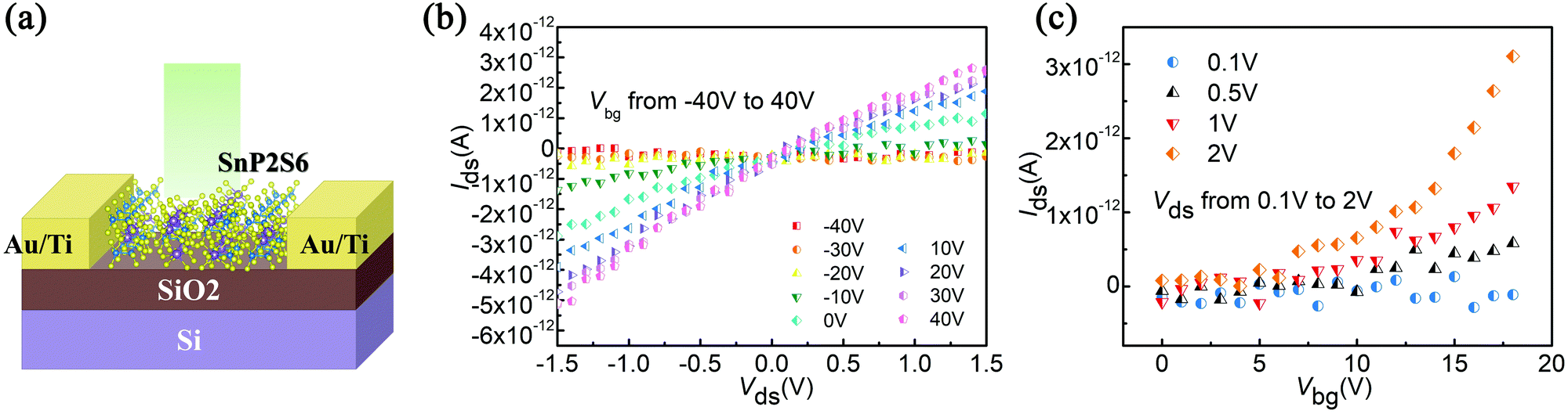 | ||
| Fig. 2 Electronic properties of back-gated FETs using SnP2S6 as the channel. (a) Schematic of the SnP2S6 photodetector on the SiO2/Si substrate, which provides the convenience of back gating. (b) Output curves (Ids–Vds) under various Vbg ranging from −40 V to 40 V. (c) Ids–Vbg curves of SnP2S6 with different Vds bias ranging from 0.1 V to 2 V. | ||
The Ids–Vds curves shown in Fig. 3(a) are linear and symmetric while sweeping bias voltages, indicating an ohmic contact. The device shows an increase of drain current by several orders of magnitude once the device is illuminated. The typical optical image of the devices is shown in the inset of Fig. 3(a) and in Fig. S2 (ESI†). Furthermore, the power dependent photocurrent is plotted using a log–log scale method in Fig. 3(b). As the incident light power increases from 0.1 to 50 mW, the photocurrent Iph increases monotonically from 8.3 × 10⁻¹² to 1.2 × 10⁻¹⁰ A with a bias of 5 V, indicating that the photocurrent is linearly proportional to the incident light power following Iph–Pβ. Moreover, as the bias voltage shifts from 0.1 to 5 V, the value of β increases from 0.23 to 0.44. The great loss of photocurrent represented by the non-unity exponent relationship and a low value of β suggests that the photocurrent is influenced by complex processes including the absorption of photons, generation of free carriers, recombination of the photogenerated free carriers, charge trapping by the defects and charge impurities in SnP2S6 flakes, scarcely lateral photoeffect38 and the adsorbed molecules at the SnP2S6/SiO2 interface.39–41
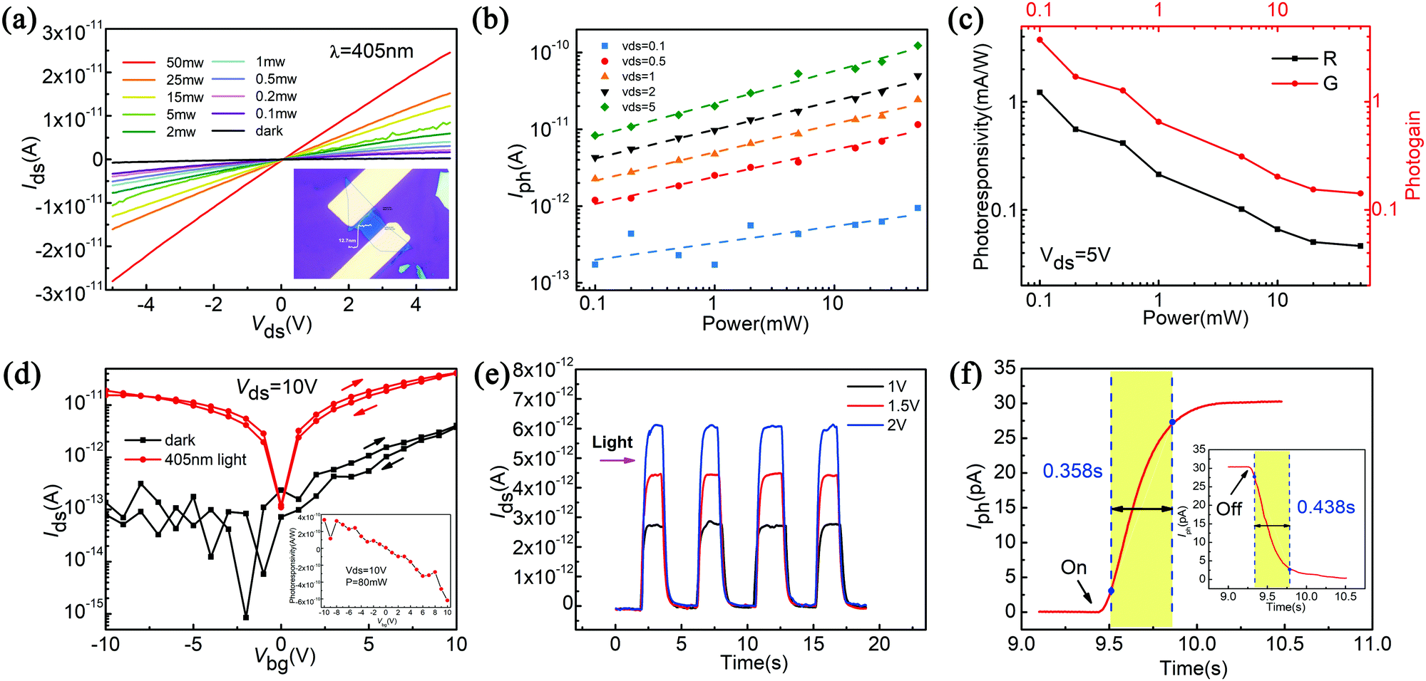 | ||
| Fig. 3 Optical properties of the SnP2S6 photodetector. (a) Ids–Vds curves of SnP2S6 at different light powers. Inset: The optical image of the device with a thickness of 12.7 nm. (b) Photocurrent (Iph) varies with light power and Vds. (c) Photoresponsivity (R) and photogain (G) varying with light power. Rmax = 1.22 mA W−1, Gmax = 3.74. (d) Ids–Vbg curves in the dark and under 405 nm light. The dark current could be reduced to the pA regime. Under light conditions, the current hysteresis box becomes small. Inset: Photoresponsivity varies with Vbg, under Vds = 10 V, P = 80 mW. (e) The ON/OFF test of photocurrent under 532 nm light and a bias from 1 V to 2 V. The ON–OFF ratio >103. (f) The exponential fitting of the dynamic response of photocurrent for the rise and decay time. The deduced rise (τrise) and decay (τdecay) time constants are about 0.358 s and 0.438 s. | ||
Meanwhile, the photoresponsivity R and photo-gain G at a drain voltage of Vds = 5 V exhibit a strong dependence on the illumination power, as shown in Fig. 3(c). The photoresponsivity R is one of the most important features for a photodetector.42R = Iph/PS, where P is the incident light power density and S is the effective illuminated area. As shown in Fig. 3(c), the photoresponsivity increases with the decrease of light power, which is possibly attributed to the less frequent carrier recombination and longer carrier lifetime under weaker illumination. This is consistent with the photoconductor-based photodetector previously reported.8,43 Photogain (G) is another parameter to evaluate the performance of a phototransistor, which can be calculated using the formula: G = (Iph/q)/(PS/hν) = hνR/q,44 where Iph is the photocurrent, q is the electron charge, h is Planck's constant, ν is the light frequency, and R is the responsivity. The value of G was estimated to reach up to 3.74 at a power of 0.1 mW.
The gate voltage dependent photoresponse of SnP2S6 is also investigated. The transfer curves under the light on and off conditions are shown in Fig. 3(d), where an incident illumination of 80 mW is applied. The curves show an increase of drain current by nearly two orders of magnitude once the device is illuminated, indicating that the photocurrent dominates in the entire operating range of the device. As can be seen from Fig. 3(d), the photocurrent shows an ambipolar behaviour with large gate-tunability.
In order to study the stability and photoresponse speed of the SnP2S6 photodetector, the time–current curves with 532 nm laser switching on and off were measured. For three different bias voltages (1 V, 1.5 V and 2 V), as shown in Fig. 3(e), the time dependent photocurrent varies periodically with regular illumination, suggesting a stable and reversible photoresponse. The response speed is evaluated according to a typical rise time/decay time, which is defined as the time span over which the photocurrent increases from 10% to 90% (or decreases from 90 to 10% analogously) when the laser is switched on and off. Fig. 3(f) shows the results of the rise and decay times of τrise = 0.358 s and τdecay = 0.438 s for Vds = 2 V, where the rising and falling parts of the curve can be fitted with an exponential function I = I0 + Aet/τrise or decay, where τrise or decay is the rise or decay time constant.
Dielectric properties of the SnP2S6 film
We first studied the temperature dependent dielectric permittivity at different frequencies. For this, bulk samples of SnP2S6 with a size of 5 × 5 × 0.05 mm3 were obtained from the gas phase. Silver paste deposited on opposite planes of the test sample was used as the electrodes. The measurements were carried out at the frequency range of 10 Hz to 50 kHz and the temperature range of 80 to 400 K. Meanwhile, a GW INSTEK LCR-819 meter and an immersed liquid nitrogen cryostat with a temperature measurement accuracy of 0.001 K were adopted. The cooling rate was 0.1 K min−1 at a measuring field strength of 1 V cm−1. As can be seen in Fig. 4(a and b), when the SnP2S6 crystals are cooled, a monotonic decrease trend in the permittivity (a) and dielectric losses (b) is observed. At high temperatures, low frequency ε′ and ε′′ increase strongly, which is most likely caused by an increase in the conductivity of the sample. The dielectric value of SnP2S6 (≈23) is much higher than that of h-BN (≈5.0), which is comparable with or higher than those of traditional high-k oxide dielectrics such as Al2O3,45 HfO2,46 and ZrO2.47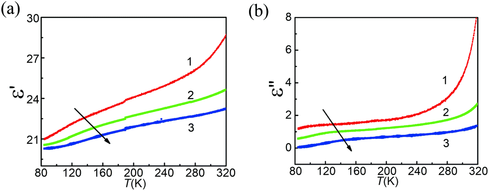 | ||
| Fig. 4 Temperature dependence of the SnP2S6 crystal dielectric permittivity of the real (a) and imaginary (b) parts at frequencies 1(1 kHz), 2(10 kHz), and 3(40 kHz). | ||
Considering that the SnP2S6 film has excellent insulating property, good chemical stability and a high dielectric constant, it shows great potential for integrating into 2D FETs as a dielectric layer to modulate the carrier density of semiconducting channel. To demonstrate its advantages in this regard, we fabricate 2D FETs and evaluate the gating effect of SnP2S6 as top-gate dielectrics.
The well-studied 2D semiconductor MoS2 was chosen as a representative channel material. Initially, we build MoS2/SnP2S6 FETs on SiO2/Si substrate (the corresponding schematic is provided in ESI† Fig. S5A), but the result shows that the hysteresis window of the devices is too big (ESI† Fig. S5C). Here, in order to reduce the hysteresis window, we use h-BN as the substrate, which can be prepared with a very uniform thickness and an atomically flat surface,48 and this method is proven to be effective in improving the performance of MoS2 FETs.49,50 The schematic illustration of our device is shown in Fig. 5(a) (optical image in ESI† Fig. S6 and S7D).
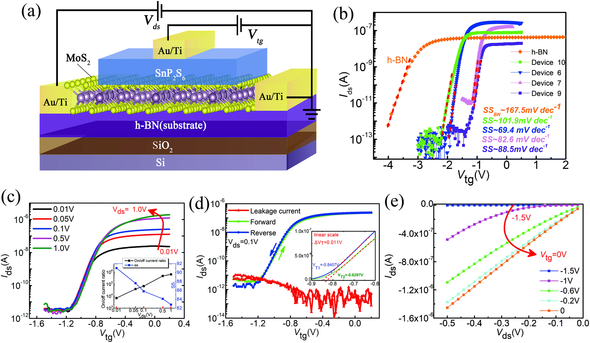 | ||
| Fig. 5 Electronic properties of top-gated MoS2 FETs using SnP2S6 as a gate dielectric. (a) Schematic of SnP2S6/MoS2 FETs using h-BN as a substrate. (b) Ids–Vtg curves of MoS2 FETs at 300 K. The orange points represent the Ids–Vtg curve of h-BN/MoS2 FET as a contrasting device, in which h-BN is thinner than SnP2S6. Others are the Ids–Vtg curves of SnP2S6/MoS2 FETs which exhibit a subthreshold slope (SS) down to 69.4 mV dec−1. (c–e) The best performance of the SnP2S6/MoS2 FET (Device 7). (c) Ids–Vtg characteristics measured at a drain bias ranging from 0.01 V to 1 V, and the inset shows the ON/OFF current ratio and SS extracted at different Vds values. (d) Double-sweep Ids–Vtg curves with a small hysteresis and leakage current, and the inset exhibiting the current on a linear scale (hysteresis gap ΔVT ≈ 0.011 V). (e) Ids–Vds characteristics measured at different Vtg values. | ||
The thin-film 2D materials are obtained through a mechanical exfoliation process (see ESI† Fig. S7A–C). Through the process described in the methods, 7 devices based on SnP2S6/MoS2 flakes with various thicknesses were fabricated. The optimal electric performance was observed in the devices with the thickness of SnP2S6 about 49.7 nm (details in ESI† Fig. S6 and S8). Meanwhile, a top-gate h-BN/MoS2 FET was also fabricated for comparison according to the schematic in ESI† Fig. S9C, in which h-BN (with a thickness of about 23.44 nm) is thinner than SnP2S6 (optical and AFM images in ESI† Fig. S6). Fig. 5(b) shows the top-gate transfer (Ids–Vtg) characteristics of the h-BN/MoS2 FET (the orange points) and four SnP2S6/MoS2 FETs on the insulating h-BN substrate (see ESI† Fig. S7D). For the former one, a subthreshold slope (SS) value of 167.5 mV dec−1 and an ON/OFF ratio of 105 were obtained. While for the latter, SnP2S6/MoS2 FETs, a small subthreshold slope (SS) value as low as 69.4 mV dec−1 of device 6 (blue points) was achieved at a drain bias of 0.1 V, which is close to the limit value51 of 60 mV dec−1. The device could even reach a high ON/OFF ratio of 107 and a high carrier mobility of 28.498 cm2 V−1 s−1 at a higher drain bias (ESI† Fig. S10(A)). The threshold voltage (Vt) is a useful parameter to describe how much voltage is needed to initiate the channel conduction. Here, Vt of the fabricated device is as low as −1.1 V (ESI† Fig. S10(B)). Thus, the FETs with a smaller SS value, low on voltage and low threshold voltage can achieve effective switching at a low Vds, thereby reducing the leakage current and power consumption of FET devices. It is remarkable for our SnP2S6 based FET to have such an excellent SS. In order to unravel the underlying mechanisms, we have carried out the following discussions. The contrast above indicates that thicker SnP2S6 films with thickness from 47.7 nm to 49.7 nm show the best performance and they have stronger gate control capability and low leakage current compared with 23.44 nm-thick h-BN. Thus, it means SnP2S6 owns a larger capacitance value than h-BN in MoS2 FETs (CSnP2S6 > Ch-BN), though SnP2S6 is thicker than h-BN (dSnP2S6 > dh-BN). According to the equation
| C = ε0εr/d |
As shown in Fig. 5(c and d), the typical SnP2S6/MoS2 device exhibits a high ON/OFF ratio and steep SS simultaneously. The effect of the increasing drain bias, resulting in an augmented drive current and steeper SS value, is displayed in (Fig. 5(c)). It can be seen that the best transistor performance is achieved at Vds = 1 V, with a maximum measured on-state current of ∼1 μA, ON/OFF current ratio close to 106, SS value as small as 82.6 mV dec−1 (inset of Fig. 5(c)) and the leakage current as low as ∼1011 A (Fig. 5(d)). The corresponding hysteresis stability of the device is demonstrated in Fig. 5(d). To describe the hysteresis stability, we introduce the hysteresis window (ΔVT), which is defined as the difference between the forward and reverse sweep threshold voltage.52 As obtained on a linear scale in the inset of Fig. 5(d), ΔVT = |VT1 − VT2| was determined as low as 0.011 V, which is a fairly small value in FETs. However, the hysteresis window became larger after two days in a glove box (ESI† Fig. S11D–F) and different hysteresis behaviours were observed in some of our devices (ESI† Fig. S11A–C). The hysteresis variation may be associated with flake quality or fabrication process in a laboratory environment, which can lead to charge trapping at the interface, adsorption/desorption of ambient molecules or atmospheric moisture in the exposed active layers.50,53 The small hysteresis could indicate that the fabricated SnP2S6/MoS2 device shows an atomic flat and sharp interface. The corresponding output (Ids–Vds) characteristics measured in the case of different Vtg values (Fig. 5(e)) show linear Ids–Vds characteristics at low drain bias and saturated current at a high drain bias.
The breakdown electric field (Vbd) is another important parameter to evaluate the strength of the insulating layer. To test the current leakage and breakdown threshold, SnP2S6 is sandwiched between two electrodes to build a vertical device as shown in the inset of Fig. S12 (ESI†). At room temperature, Vbg is fixed at 0 V, and Vds is swept.54 The Ids–Vds curve is plotted in Fig. S12 (ESI†), where the initial low current increases slowly as the Vds value increases. The current increases dramatically once Vds approaches Vbd. After the breakdown, the device is permanently destroyed as a large current flows across SnP2S6. Vbd is estimated to be about 5 V (with a thickness of 26.5 nm), and the corresponding breakdown electric field Fbd could reach as high as 1.9 MV cm−1.
Furthermore, to investigate the optoelectronic properties of our FETs, we put one of our SnP2S6/MoS2 FETs (Device 9, its optical image in the inset of Fig. 6(b)) under 405 nm laser irradiation of 80 mW. The output and transfer characteristics in the dark (black), under 405 nm irradiation (blue) and after irradiation (red) are separately depicted in Fig. 6(b and c). Under illumination, the output characteristic of the device remains linear while the reduced electrical resistance of the semiconductor was obseved due to the photoconductive effect (PC effect), where the extra free carriers are generated by the photon absorption (Fig. 6(b)). Meanwhile, as shown in Fig. 6(c), a significant change in the threshold voltage was also observed when illuminated by 405 nm light. The shifting of the threshold voltage to the negative Vtg side is known as the photogating effect (PG effect). The PG effect is a phenomenon in which photogenerated holes get trapped and then attract more electrons, thus gradually increasing the channel conductivity.55,56
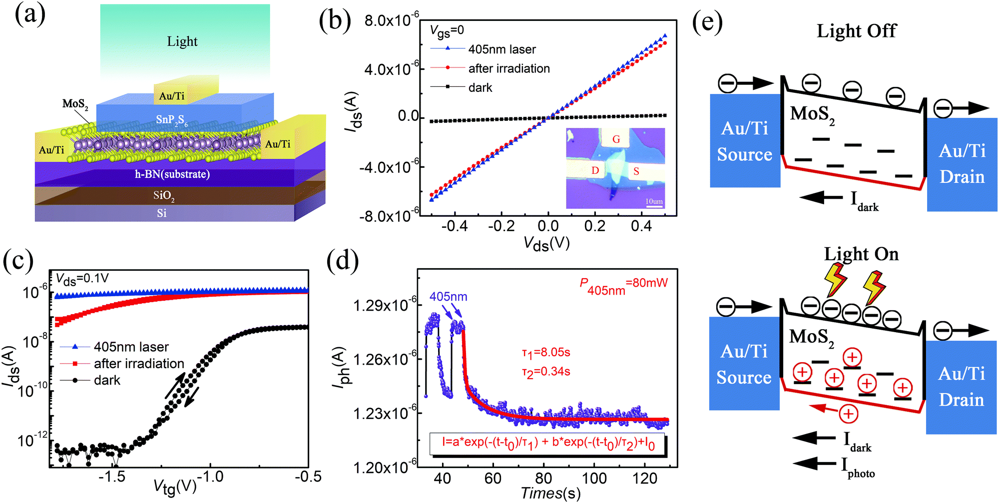 | ||
| Fig. 6 Optical properties of top-gated SnP2S6/MoS2 FETs. (a) Schematic diagram of photogating dominated SnP2S6/MoS2 FETs (Device 9). (b) Typical Ids–Vds characteristics of Device 9 in the dark (black), under illumination (blue) and after irradiation (red), and the inset showing the optical image of the FET. (c) Ids–Vtg characteristics showing transfer curve shifts in the negative Vtg direction under and after irradiation. (d) Photocurrent decay after a longer light pulse with longer (τ1 ∼ 8.05 s) and shorter (τ2 ∼ 0.34 s) time constants, which corresponds to (b) and (c). (e) Band diagram of the device without (top panel) and with light (bottom panel), showing hole trapping in shallower and deeper trap states close to the valence band. | ||
In Fig. 6(c), compared with the initial device in the dark, the off-state current after irradiation is dramatically increased by more than five orders of magnitude at the same Vtg, implying a long-time decay of the photoconductive state. As shown in Fig. S13 (ESI†), SnP2S6 has little effect on the optical response and persistent photocurrent of the device. Therefore, to explore the photocurrent decay of the device, we then check the transient characteristics by measuring the source–drain current at a fixed Vtg = 0 V in Fig. 6(d). An abrupt increase in Ids was observed under 405 nm laser illumination, as a result of photoexcitation, followed by a much slower current increase. A very slow decay of the current can be observed when the light was switched off. This is because the trapped charges in the PG effect cause long sustained conductivity.56 In order to quantify the trapping time constant, transient data were fitted with a biexponential equation57
| I = I0 + Ae(t−t0)/τ1 + Be(t−t0)/τ2 |
Finally, the good stability, reliability and reproducibility of the devices are summarized as shown in Fig. S16–S19 (ESI†).
To highlight the performance of the SnP2S6 dielectric, the main set of achievements of the present study, such as the dielectric constant, SS value and ON/OFF ratio, are presented in Table 1. Compared with other new 2D dielectric materials, the excellent performance of SnP2S6 is comparable to or even better than those of these materials.
Conclusion
In this paper, we have systematically investigated the photoelectric and electrical properties of a novel 2D SnP2S6 crystal. Moreover, it was integrated into MoS2 based FETs to serve as a top gate dielectric. The results demonstrate its excellent properties including a large dielectric constant (≈23, compared with h-BN), a fairly small SS value (as low as 69.4 mV dec−1), a high ON/OFF ratio (reaching 107), a negligible hysteresis, and a considerable breakdown voltage (≈1.9 MV cm−1). Due to its good photoelectric properties, good reliability and reproducibility (0.5 standard deviation of threshold voltage), SnP2S6 could become a potential candidate for the construction of advanced optoelectronic and electronic devices.Methods
Material characterization
Raman spectra are recorded using a Horiba confocal Raman system with an excitation laser of 532 nm. The morphology characterization and thickness calibration of the SnP2S6 film as well as thickness measurement of h-BN and MoS2 are carried out with an optical microscope and AFM instruments.Fabrication of an SnP2S6 phototransistor and SnP2S6/MoS2 FET devices
An SnP2S6 phototransistor was fabricated by exfoliating thin flakes onto heavily doped silicon substrates. The top electrodes are defined using a standard photolithography process followed by thermal evaporation of the Ti/Au metal, and a lift-off process. We have built three batches of SnP2S6/MoS2 devices on a SiO2/Si substrate and an h-BN substrate, respectively. Thin-film 2D materials are obtained through a mechanical exfoliation process first. Then, the 2D nanosheets of top-gate FETs are stacked up by a polydimethylsiloxane (PDMS) assisted transfer technique onto an h-BN nanosheet to develop heterostructures. The source–drain and gate electrodes Ti/Au of each device were patterned and deposited by photolithography and a lift-off process. Preparation methods for other devices including back-gate FETs and top-gate FETs on different substrates adjust according to their schematic.Electrical and optical characterization measurements
We tested the device directly after fabrication. Electrical and photoelectrical characterization of devices including ID–VG, ID–VD and Iph–t involved measurements were performed under vacuum condition at room temperature (300 K) using a probe station.Author contributions
J. H. and A. Z. carried out the electrical and optoelectronic measurements. E. P., J. C. and R. B. assisted in the device fabrication and electrical measurement. E. P. carried out the AFM measurement. J. L. and X. J. carried out the Raman characterization. A. M. and Y. V. conducted dielectric measurement and crystal growth. Q. L., G. C. and P. M. analyzed the data. J. H., A. Z. and F. L. wrote the manuscript. Q. L. and G. C. revised the manuscript. F. L. supervised the project. All the authors commented on the manuscript.Conflicts of interest
There are no conflicts to declare.Acknowledgements
F. L. acknowledges the support from the National Natural Science Foundation of China (62074025,12161141015), the National Key Research & Development Program (2021YFE0194200, 2020YFA0309200), the Applied Basic Research Program of Sichuan Province (2021JDGD0026), and the Sichuan Province Key Laboratory of Display Science and Technology.References
- Y. Liu, N. O. Weiss, X. Duan, H.-C. Cheng, Y. Huang and X. Duan, Nat. Rev. Mater., 2016, 1, 16042 CrossRef CAS.
- A. K. Geim and I. V. Grigorieva, Nature, 2013, 499, 419–425 CrossRef CAS PubMed.
- G. B. Liu, D. Xiao, Y. Yao, X. Xu and W. Yao, Chem. Soc. Rev., 2015, 44, 2643–2663 RSC.
- L. Mennel, J. Symonowicz, S. Wachter, D. K. Polyushkin, A. J. Molina-Mendoza and T. Mueller, Nature, 2020, 579, 62–66 CrossRef CAS PubMed.
- F. Schwierz and M. Ziegler, Presented in part at the 2021 IEEE Latin America Electron Devices Conference (LAEDC), 2021.
- T. Tan, X. Jiang, C. Wang, B. Yao and H. Zhang, Adv. Sci., 2020, 7, 2000058 CrossRef CAS PubMed.
- J. Chen, G. Cao, Q. Liu, P. Meng, Z. Liu and F. Liu, Rare Met., 2022, 41, 325–332 CrossRef CAS.
- P. Yu, Q. Zeng, C. Zhu, L. Zhou, W. Zhao, J. Tong, Z. Liu and G. Yang, Adv. Mater., 2021, 33, e2005607 CrossRef PubMed.
- C. Y. Zhu, J. K. Qin, P. Y. Huang, H. L. Sun, N. F. Sun, Y. L. Shi, L. Zhen and C. Y. Xu, Small, 2022, 18, e2104401 CrossRef PubMed.
- Y. Chen, W. Ma, C. Tan, M. Luo, W. Zhou, N. Yao, H. Wang, L. Zhang, T. Xu, T. Tong, Y. Zhou, Y. Xu, C. Yu, C. Shan, H. Peng, F. Yue, P. Wang, Z. Huang and W. Hu, Adv. Funct. Mater., 2021, 31, 2009554 CrossRef CAS.
- T. Tong, Y. Chen, S. Qin, W. Li, J. Zhang, C. Zhu, C. Zhang, X. Yuan, X. Chen, Z. Nie, X. Wang, W. Hu, F. Wang, W. Liu, P. Wang, X. Wang, R. Zhang and Y. Xu, Adv. Funct. Mater., 2019, 29, 1905806 CrossRef CAS.
- X. Zou, Y. Xu and W. Duan, Innovation, 2021, 2, 100115 Search PubMed.
- G. Cao, P. Meng, J. Chen, H. Liu, R. Bian, C. Zhu, F. Liu and Z. Liu, Adv. Funct. Mater., 2021, 31, 2005443 CrossRef CAS.
- I. Ferain, C. A. Colinge and J. P. Colinge, Nature, 2011, 479, 310–316 CrossRef CAS PubMed.
- I. Cunha, R. Barras, P. Grey, D. Gaspar, E. Fortunato, R. Martins and L. Pereira, Adv. Funct. Mater., 2017, 27, 1606755 CrossRef.
- P. Barquinha, L. Pereira, G. Goncalves, R. Martins, D. Kuščer, M. Kosec and E. Fortunato, J. Electrochem. Soc., 2009, 156, H824 CrossRef CAS.
- Y. Y. Illarionov, T. Knobloch, M. Jech, M. Lanza, D. Akinwande, M. I. Vexler, T. Mueller, M. C. Lemme, G. Fiori, F. Schwierz and T. Grasser, Nat. Commun., 2020, 11, 3385 CrossRef CAS PubMed.
- F. Hui, C. Pan, Y. Shi, Y. Ji, E. Grustan-Gutierrez and M. Lanza, Microelectron. Eng., 2016, 163, 119–133 CrossRef CAS.
- T. Knobloch, Y. Y. Illarionov, F. Ducry, C. Schleich, S. Wachter, K. Watanabe, T. Taniguchi, T. Mueller, M. Waltl, M. Lanza, M. I. Vexler, M. Luisier and T. Grasser, Nat. Electron., 2021, 4, 98–108 CrossRef CAS.
- M. Lin, P. Liu, M. Wu, Y. Cheng, H. Liu, K. Cho, W.-H. Wang and F. Lu, Appl. Surf. Sci., 2019, 493, 1334–1339 CrossRef CAS.
- I. P. Studenyak, V. V. Mitrovcij, G. S. Kovacs, M. I. Gurzan, O. A. Mykajlo, Y. M. Vysochanskii and V. B. Cajipe, Phys. Status Solidi B, 2003, 236, 678–686 CrossRef CAS.
- I. P. Studenyak, O. A. Mykajlo, V. O. Stephanovich, M. I. Gurzan, Y. M. Vysochanskii and V. B. Cajipe, Phys. Status Solidi A, 2003, 198, 487–494 CrossRef CAS.
- I. Studenyak, O. Mykajlo, Y. M. Vysochanskii and V. Cajipe, J. Phys.: Condens. Matter, 2003, 15, 6773 CrossRef CAS.
- K. Z. Rushchanskii, Y. M. Vysochanskii, V. B. Cajipe and X. Bourdon, Phys. Rev. B, 2006, 73, 115115 CrossRef.
- Y. M. Vysochanskii, D. Baltrunas, A. A. Grabar, K. Mazeika, K. Fedyo and A. Sudavicius, Phys. Status Solidi B, 2009, 246, 1110–1117 CrossRef CAS.
- Y. Gao, S. Lei, T. Kang, L. Fei, C. L. Mak, J. Yuan, M. Zhang, S. Li, Q. Bao, Z. Zeng, Z. Wang, H. Gu and K. Zhang, Nanotechnology, 2018, 29, 244001 CrossRef PubMed.
- B. L. Chittari, Y. Park, D. Lee, M. Han, A. H. MacDonald, E. Hwang and J. Jung, Phys. Rev. B, 2016, 94, 184428 CrossRef.
- Z. Zhu, X. Chen, W. Li and J. Qi, Appl. Phys. Lett., 2019, 114, 223102 CrossRef.
- W. Huang, F. Wang, L. Yin, R. Cheng, Z. Wang, M. G. Sendeku, J. Wang, N. Li, Y. Yao and J. He, Adv. Mater., 2020, 32, e1908040 CrossRef PubMed.
- Y. Jing, Z. Zhou, J. Zhang, C. Huang, Y. Li and F. Wang, Phys. Chem. Chem. Phys., 2019, 21, 21064–21069 RSC.
- Z. Wang, R. D. Willett, R. A. Laitinen and D. A. Cleary, Chem. Mater., 1995, 7, 856–858 CrossRef CAS.
- V. Haborets, K. Glukhov, J. Banys and Y. Vysochanskii, Integr. Ferroelectr., 2021, 220, 90–99 CrossRef CAS.
- Y. Zhang, F. Wang, X. Feng, Z. Sun, J. Su, M. Zhao, S. Wang, X. Hu and T. Zhai, Nano Res., 2021, 15, 2391–2398 CrossRef.
- I. P. Studenyak, V. V. Mitrovcij, G. S. Kovacs, O. A. Mykajlo, M. I. Gurzan and Y. M. Vysochanskii, Ferroelectrics, 2001, 254, 295–310 CrossRef CAS.
- Y. Hattori, T. Taniguchi, K. Watanabe and K. Nagashio, ACS Nano, 2015, 9, 916–921 CrossRef CAS PubMed.
- Z. Wang, R. D. Willett, R. A. Laitinen and D. A. Cleary, Chem. Mater., 1995, 7, 856–858 CrossRef CAS.
- Y. M. Vysochanskii, V. Stephanovich, A. Molnar, V. Cajipe and X. Bourdon, Phys. Rev. B, 1998, 58, 9119 CrossRef CAS.
- R. Martins and E. Fortunato, Rev. Sci. Instrum., 1995, 66, 2927–2934 CrossRef CAS.
- W. Zhang, J. K. Huang, C. H. Chen, Y. H. Chang, Y. J. Cheng and L. J. Li, Adv. Mater., 2013, 25, 3456–3461 CrossRef CAS PubMed.
- F. Gonzalez-Posada, R. Songmuang, M. Den Hertog and E. Monroy, Nano Lett., 2012, 12, 172–176 CrossRef CAS PubMed.
- X. Zhou, L. Gan, W. Tian, Q. Zhang, S. Jin, H. Li, Y. Bando, D. Golberg and T. Zhai, Adv. Mater., 2015, 27, 8035–8041 CrossRef CAS PubMed.
- O. Lopez-Sanchez, D. Lembke, M. Kayci, A. Radenovic and A. Kis, Nat. Nanotechnol., 2013, 8, 497–501 CrossRef CAS PubMed.
- G. Konstantatos, M. Badioli, L. Gaudreau, J. Osmond, M. Bernechea, F. P. Garcia de Arquer, F. Gatti and F. H. Koppens, Nat. Nanotechnol., 2012, 7, 363–368 CrossRef CAS PubMed.
- X. Xie, S. Y. Kwok, Z. Lu, Y. Liu, Y. Cao, L. Luo, J. A. Zapien, I. Bello, C. S. Lee, S. T. Lee and W. Zhang, Nanoscale, 2012, 4, 2914–2919 RSC.
- J. Robertson, Rep. Prog. Phys., 2005, 69, 327 CrossRef.
- Y.-S. Lin, R. Puthenkovilakam and J. Chang, Appl. Phys. Lett., 2002, 81, 2041–2043 CrossRef CAS.
- Y.-S. Lin, R. Puthenkovilakam, J. Chang, C. Bouldin, I. Levin, N. V. Nguyen, J. Ehrstein, Y. Sun, P. Pianetta and T. Conard, J. Appl. Phys., 2003, 93, 5945–5952 CrossRef CAS.
- K. Zhang, Y. Feng, F. Wang, Z. Yang and J. Wang, J. Mater. Chem. C, 2017, 5, 11992–12022 RSC.
- Y. Ji, C. Pan, M. Zhang, S. Long, X. Lian, F. Miao, F. Hui, Y. Shi, L. Larcher, E. Wu and M. Lanza, Appl. Phys. Lett., 2016, 108, 012905 CrossRef.
- C. Lee, S. Rathi, M. A. Khan, D. Lim, Y. Kim, S. J. Yun, D. H. Youn, K. Watanabe, T. Taniguchi and G. H. Kim, Nanotechnology, 2018, 29, 335202 CrossRef PubMed.
- R. K. Jana, G. L. Snider and D. Jena, Phys. Status Solidi C, 2013, 10, 1469–1472 CrossRef CAS.
- D. Estrada, S. Dutta, A. Liao and E. Pop, Nanotechnology, 2010, 21, 85702 CrossRef PubMed.
- Y. Y. Illarionov, A. G. Banshchikov, D. K. Polyushkin, S. Wachter, T. Knobloch, M. Thesberg, L. Mennel, M. Paur, M. Stöger-Pollach, A. Steiger-Thirsfeld, M. I. Vexler, M. Waltl, N. S. Sokolov, T. Mueller and T. Grasser, Nat. Electron., 2019, 2, 230–235 CrossRef CAS.
- X. Yan, I. S. Esqueda, J. Ma, J. Tice and H. Wang, Appl. Phys. Lett., 2018, 112, 032101 CrossRef.
- A. Di Bartolomeo, L. Genovese, T. Foller, F. Giubileo, G. Luongo, L. Croin, S. J. Liang, L. K. Ang and M. Schleberger, Nanotechnology, 2017, 28, 214002 CrossRef PubMed.
- M. Buscema, J. O. Island, D. J. Groenendijk, S. I. Blanter, G. A. Steele, H. S. van der Zant and A. Castellanos-Gomez, Chem. Soc. Rev., 2015, 44, 3691–3718 RSC.
- D. J. Late, B. Liu, H. S. Matte, V. P. Dravid and C. N. Rao, ACS Nano, 2012, 6, 5635–5641 CrossRef CAS PubMed.
- B. Chamlagain, Q. Cui, S. Paudel, M. M.-C. Cheng, P.-Y. Chen and Z. Zhou, 2018, arXiv:1808.08303 DOI:10.48550/arXiv.1808.08303.
- T. Li, T. Tu and Y. Sun, Nat. Electron., 2020, 3, 473–478 CrossRef CAS.
- K. Liu, B. Jin, W. Han, X. Chen, P. Gong, L. Huang, Y. Zhao, L. Li, S. Yang, X. Hu, J. Duan, L. Liu, F. Wang, F. Zhuge and T. Zhai, Nat. Electron., 2021, 4, 906–913 CrossRef CAS.
Footnotes |
| † Electronic supplementary information (ESI) available. See DOI: https://doi.org/10.1039/d2tc01340a |
| ‡ These authors contributed equally. |
| This journal is © The Royal Society of Chemistry 2022 |