
 Open Access Article
 This Open Access Article is licensed under a
 Creative Commons Attribution 3.0 Unported Licence
Charge transport materials for mesoscopic perovskite solar cells
Maria
Vasilopoulou
 *a,
Anastasia
Soultati
a,
Petros-Panagis
Filippatos
ab,
Abd. Rashid bin
Mohd Yusoff
c,
Mohhamad Khadja
Nazeeruddin
*d and
Leonidas C.
Palilis
*e
*a,
Anastasia
Soultati
a,
Petros-Panagis
Filippatos
ab,
Abd. Rashid bin
Mohd Yusoff
c,
Mohhamad Khadja
Nazeeruddin
*d and
Leonidas C.
Palilis
*e
aInstitute of Nanoscience and Nanotechnology (INN), National Center for Scientific Research “Demokritos”, 15341 Agia Paraskevi, Attica, Greece. E-mail: m.vasilopoulou@inn.demokritos.gr
bFaculty of Engineering, Environment and Computing, Coventry University, Priory Street, Coventry CV1 5FB, UK
cDepartment of Chemical Engineering, Pohang University of Science and Technology (POSTECH), Pohang, Gyeongbuk 37673, Republic of Korea
dInstitute of Chemical Sciences and Engineering, École Polytechnique Fédérale de Lausanne (EPFL), Rue de l’Industrie 17, CH-1951 Sion, Switzerland. E-mail: MdKhaja.Nazeeruddin@epfl.ch
eDepartment of Physics, University of Patras, 26504 Rio – Patra, Greece. E-mail: lpalilis@physics.upatras.gr
First published on 12th July 2022
Abstract
Organic–inorganic perovskite solar cells have achieved an impressive power conversion efficiency of up to 25.6% and 24.8%, respectively, for single and multijunction tandem architectures due to the huge progress made in the rational design and development of both the perovskite absorbers and the charge transport and electrode materials used as the selective contacts. The interfaces between the perovskite film and the charge transport layers are among the most critical factors in determining the efficiency and stability of perovskite solar cells regardless of the structure employed (mesoporous (mp) or planar heterostructure). Herein, an overview is provided on the recent advances in the fundamental understanding of how these interfaces, upon incorporating various functional charge transport layers, influence the performance of mp perovskite solar cells (mp-PSCs) where the perovskite is deposited and embedded in a high porosity and surface area mp material. First, the most critical aspects of such materials that govern the performance of the complete device are discussed including the energy level alignment at the interfaces, charge transport in interfacial layers, defects in the perovskite, interfacial layers or at their interfaces, as they all strongly affect interfacial charge recombination and extraction. In this context, we will discuss the various strategies for the interfaces and the interfacial materials employed both for the hole (HTM) and electron (ETM) transport/extraction. Next, advances in the performance of a highly promising alternative mp architecture, namely HTM-free triple mp-PSCs, where the HTL is removed to reduce complexity and manufacturing cost for printable mp PSCs, will be discussed. Finally, an outlook for the development of highly efficient and stable mpPSCs will be provided.
 Maria Vasilopoulou | Dr Maria Vasilopoulou is a Senior Researcher at the Institute of Nanoscience and Nanotechnology of the National Center for Scientific Research “Demokritos” (NCSRD), Greece. She received her Physics BSc from the University of Athens and her PhD in Functional Materials for Nanolithography from the Chemical Engineering Department of the National Technical University of Athens. Then, she worked as postdoctoral researcher at NCSRD where she developed materials as interfacial layers in organic solar cells and light emitting diodes. Her research focuses on organic and perovskite optoelectronic devices, mainly on interfaces characterization. She has more than 100 publications and holds five patents. |
 Anastasia Soultati | Dr Anastasia Soultati is a postdoctoral researcher at NCSRD in Athens, Greece. During 2021 and 2016 worked as adjunct assistant professor in the Department of Materials Science in the University of Patras and the Department of Electrical and Electronics Engineering of University of West Attica. She received a degree in Physics and a MSc in Microelectronics from the University of Athens in 2009 and 2012, respectively, and her PhD from the Chemical Engineering Department of National Technical University of Athens in 2016. Her current research focuses on the area of interface engineering in organic and perovskite optoelectronic devices. |
 Petros-Panagis Filippatos | Petros Panagis Filippatos was born in Athens, Greece. He received the MEng degree in Electrical and Computer Engineering from the National Technical University of Athens. He is currently a PhD student at Coventry University and NCSR Demokritos. His research interests involve Li-ion Batteries, Photovoltaics, Hydrogen Production and Gas Sensors. |
 Abd. Rashid bin Mohd Yusoff | Dr Abd. Rashid Mohd Yusoff obtained his BSc in Physics from Universiti Putra Malaysia in 2002. In 2011, he completed his PhD at the Universidade Federal do Paraná, Brazil. From 2011 to 2013 he was a Postdoc Fellow working at the Department of Information Display, Kyung Hee University. He then worked as a Research Professor until 2018, when he joined the Sêr SAM group at Swansea University. Dr Muhd Yusoff is a Senior Research Fellow with Sêr SAM with a focus on perovskite photovoltaics. His research interests include photovoltaics, light emitting diodes, transistors and photochemical water splitting. |
 Mohhamad Khadja Nazeeruddin | Prof. Mohammad K. Nazeeruddin is a Professor at EPFL, Switzerland (https://gmf.epfl.ch/). His current research focuses on Perovskite and Dye-Sensitized Solar Cells and Light-emitting diodes. He has published more than 700 peer-reviewed papers, ten book chapters, and an inventor/co-inventor of over 75 patents. He has been named Thomson Reuters “Highly Cited Researcher” since 2014, and one of the 19 scientists identified by Thomson Reuters as The World's Most Influential Scientific Minds 2016 and 2017 from all scientific domains. He has appeared in the ISI listing of most cited chemists and has more than 99 |
Dr Leonidas Palilis is an Associate Professor at the University of Patras, Greece. He obtained his BSc in Physics from the University of Athens. He received his PhD in physics from the University of Sheffield, UK, in 2001. He then joined the Naval Research Laboratory in Washington, DC, as a postdoctoral researcher and, subsequently, the NCSRD as a collaborating researcher. His research interests focus on various optoelectronic materials and devices for organic electronics and photonics with emphasis on light-emitting diodes and solar cells. He has more than 70 publications and his work has received more than 3500 citations. |
1. Introduction
Perovskite solar cells (PSCs) are based on hybrid organic–inorganic halide perovskite light-harvesting materials with a chemical structure ABX3; A, B representing cations, typically A is an organic cation such as CH3CH3 (methylammonium, MA) or NH2CHNH2 (formamidinium, FA) or a mixed cation and B is a metal cation such as Pb or Sn whereas X is an anion, typically I, Cl, Br, that bonds to both A and B. Recently, they have emerged as the most promising photovoltaic technology, rivaling commercialized silicon solar cells, as they exhibit outstanding power conversion efficiencies (PCEs) for single junction1 and multijunction tandem architectures2 combined with decent ambient and thermal stability, despite the many defects and grain boundaries (GBs) inherently present in these materials. In particular, single junction PSCs1 with an impressive PCE of 25.6% and long-term operational stability of 450 h have been demonstrated by appropriate anion engineering to suppress anion-vacancy defects present at GBs and at the perovskite film surface and increase film crystallinity. Lin et al. reported a strategy to reduce Sn defects (vacancies) in mixed Pb–Sn narrow-bandgap perovskites, thereby increasing the charge-carrier diffusion length to 3 μm and demonstrating a PCE of 21.1% for 1.22 eV narrow-bandgap perovskites in a single-junction configuration and monolithic all-perovskite tandem cells with certified PCEs of 24.8% for small-area devices (0.049 cm2) and of 22.1% for large-area devices (1.05 cm2).2 Remarkably, the tandem cells retained 90% of their initial PCE after 463 h of continuous operation. Combining organic and perovskite materials with an optimized interconnecting layer structure has recently resulted in perovskite/organic tandem solar cells with a maximum PCE of 23.6% which is retained to nearly 90% after 500 h continuous illumination.3 On the other hand, combination of perovskites with silicon resulted in a monolithic tandem silicon/perovskite cell with a 1.68 eV bandgap perovskite which retained 95% of its initial PCE of 29% after 300 h of operation as reported by Al-Ashouri et al.4Notably, the highest PCE values have been demonstrated upon employing a mesoporous PSC architecture (mp-PSC),5 in which typically highly transparent mp metal oxides combining a high porosity and large surface area are used as electron transporting materials/layers (ETMs/ETLs) (e.g. titanium dioxide (TiO2),6 tin oxide (SnO2)7) or, alternatively as hole transporting materials/layers (HTMs/HTLs) (e.g. nickel oxide (NiOx)8). Mp ETLs/HTLs have been shown to facilitate perovskite infiltration as well as improve the physical contact and increase the interfacial area between the perovskite and the selective electrode, thus resulting in rapid, more efficient and selective, electron/hole extraction from the active layer, while blocking opposite carrier transport and suppressing undesirable interfacial recombination.9 Note, that in contrast, planar heterostructure devices are based on planar HTLs and/or ETLs.10 A schematic diagram illustrating exciton formation upon solar light illumination, charge transfer and recombination processes in representative PSCs is depicted in Fig. 1.
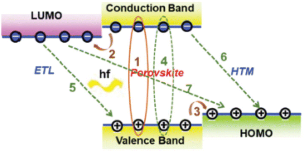 | ||
| Fig. 1 Schematic diagram illustrating exciton formation upon solar illumination with photon energy hf (1), charge transfer (electron (2) and hole (3)) and recombination (4, 5, 6, 7) processes in PSCs employing both an ETL and a HTM to transport electrons and holes, respectively. Thick and thin lines, respectively, indicate processes desirable for efficient performance and recombination-induced losses. Reprinted with permission from ref. 9. Copyright 2020 Royal Society of Chemistry. | ||
With regard to mp-PSCs, devices with a mp-ETL denote a regular conventional n–i–p architecture whereas a mp-HTL typically is used in an inverted p–i–n architecture (depending on the sequence of the device layers).5 Moreover, advances in device architecture have resulted in the demonstration of highly efficient mp-PSCs without the need for a HTL (termed as HTM-free triple mp-PSCs11) in the n–i–p configuration typically having a mp-TiO2 ETL, a mp insulating spacer layer (such as ZrO2 or Al2O3) and a mp carbon counter electrode (CE) that can be printable with various roll-to-roll (R2R) fully compatible processes and methods. In a typically triple mesoscopic TiO2/ZrO2/carbon CE architecture, the thickness of the spacer layer, loading amount and morphology of perovskite as well as the substrate and precursor solution temperature can be separately or, even, simultaneously optimized to enhance both light-harvesting ability and charge transport.12,13 Representative architectures for mp-PSCs are shown in Fig. 2.
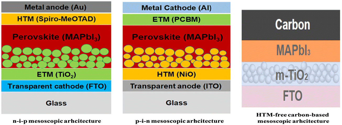 | ||
| Fig. 2 Representative n–i–p, p–i–n and HTM-free carbon-based m-PSC architectures employing MAPbI3 as the photoactive perovskite layer, m-TiO2 as the ETL and an organic p-type small molecule (namely spiro-MeOTAD) in the n–i–p structure and m-NiO as the HTL and an organic n-type small molecule (namely PCBM) as the ETL in the p–i–n structure. Reprinted with permission from ref. 5 and 10, respectively. Copyright 2016 SPIE and Copyright 2022 Elsevier, respectively. | ||
Evidently, in depth understanding of the operational principles of PSCs such as charge generation, exciton dissociation, carrier transport and extraction/collection and the potential limitations associated with perovskite film defects and GBs are highly critical in order to improve device performance and stability en route to possible commercialization of this breakthrough technology. Particularly, as interfaces between the electrodes and the perovskite layer play a decisive role in both device efficiency and stability,14 interfacial engineering using appropriate functional materials is a key strategy employed to optimize overall device performance.15 The aims of this strategy are multifold: (i) to enhance interfacial charge transport, (ii) to improve charge extraction, and (iii) to reduce interfacial recombination either by optimizing the interfacial energy level alignment16 or by passivating interfacial, surface and/or bulk defects present in the perovskite or at the respective interfaces.17 These can fulfilled by incorporating suitable charge transport materials to adjust interface energetics,18 by treating/modifying the perovskite active layer with various materials for defect passivation19 or by simultaneously improving interfacial charge transport and passivating perovskite defects.20
Despite the fact that there have been recent reviews referring to mp-PSCs with different charge transport materials (either as HTLs21 or as ETLs22) and HTM-free mp-PSCs,23 to the best of our knowledge there has not been a review covering a wide range of materials employed for both electron hole transport and as CEs in mp-PSCs. Therefore, herein we aim to provide a critical overview of recent advances made in the fundamental understanding of how interfaces, upon incorporating various functional charge transport layers, influence the performance of mp-PSCs. In this context, we will discuss in detail various interfacial engineered strategies with a particular focus on the most advanced interfacial materials employed both for hole and electron transport/extraction. Furthermore, progress in the performance of HTM-free mp-PSCs will be reviewed in particular with regard to the various mp-ETLs, insulating and carbon-based or other novel alternative CE materials explored so far. At the end, an outlook for the development of highly efficient and stable mp-PSCs will be provided.
2. Selection criteria for efficient charge transport materials in mp-PSCs
Suitable materials selected to be employed as charge transport layers (HTL or ETLs) in mp-PSCs should fulfill certain criteria and possess specific functionalities: (i) compatible, graded, energy levels (valence band, VB, or highest occupied molecular orbital, HOMO, and conduction band, CB, or lowest unoccupied molecular orbital, LUMO, with regard to those of the perovskite – see Fig. 1) for optimized interfacial energy alignment in order to facilitate, barrier-free (or minimize the respective barrier), charge transfer and extraction and suppress carrier recombination at the electrode/perovskite interfaces by blocking the opposite carriers (i.e. charge selectivity), (ii) high electronic conductivity and carrier mobility combined with a long carrier diffusion length and a appropriately large carrier lifetime to prevent carrier losses, (iii) Large optical bandgap with a high transparency across the visible and near infrared and an appropriate extinction coefficient to allow solar light to enter the perovskite active layer without absorption losses combined with a suitable (matched to the perovskite) refractive index to allow efficient light in-coupling without reflection losses – ideally, exhibiting complementary absorption to that of the perovskite so as to absorb photons in the UV and enhance cell photocurrent, (iv) enhanced hydrophobicity in order to not allow moisture ingress in the perovskite and, thus, avoid its long-term degradation, (v) excellent, pinhole-free, uniform, conformal layer morphology preventing carrier shunting between the electrode contact and the perovskite film and being able to fill pores in the perovskite film with increased interfacial contact area, (vi) acting as a suitable template in order to tune the crystal quality of the perovskite film, to increase its grain size and enhance perovskite crystallinity, (vii) functioning as a buffer/passivation layer to reduce or passivate surface and interfacial trap states and/or suppress perovskite ion migration, thus reducing cell current–voltage hysteresis in the forward and scan directions, (viii) intrinsic stability under thermal stress and solar illumination to avoid interfacial degradation upon operation at various working conditions as well as high resistance against moisture and oxygen combined with chemical stability against possible photochemical interactions with the perovskite layer, (ix) nontoxicity and low material cost combined with simple, facile, economical and environmentally friendly processing such as spin coating or inkjet printing (ideally processing from solution, in particular upon employing organic solvents that do not attack the perovskite layer).Concerning the mp scaffold, appropriate film porosity and a high surface-to-volume ratio with an increased surface area compared to compact layers are of paramount importance for improved pore filling as the mp scaffold pore size will determine perovskite grain growth. Dense agglomeration of employed, for example, nanoparticles (NPs) and their defect density should be minimized in order to facilitate perovskite infiltration and crystallization and reduce surface/bulk or interfacial recombination as well as light scattering/reflection (thus, to enhance light trapping). Moreover, the scaffold should be appropriately designed to accelerate formation of heterogeneous nucleation sites and lead to enhanced perovskite film quality combined with uniform coverage.
3. Electron transport materials in mp-PSCs
3.1 mp-ETLs employed in n–i–p mp-PSCs
Mp electron transporting materials (mp-ETMs) have been extensively studied in the last decade, and their effective application in PSCs with a n–i–p architecture has been shown to depend on their optoelectronic and morphological properties upon modifying the ETL/perovskite interface characteristics, as well as, improving electron transport and extraction, and thus enhancing the overall device performance.24In particular, TiO2 has been the most widely employed mp ETL in mp-PSCs due to its high transparency, good electron mobility, well-matched energy levels with that of the perovskite absorber, and solution-based processing.25 Various methods have been used for the preparation of TiO2 NPs in its three different crystalline phases anatase, rutile and brookite.26 For example, Kong et al. prepared a low-temperature solution-processed brookite mp-TiO2 and employed it in mp-PSCs.27 The fabricated mp-PSCs with the brookite TiO2 ETL exhibited higher fill factor (FF) and improved open-circuit voltage (VOC) compared with the device based on the anatase TiO2. Lee et al. reported the effect of the crystalline phase of TiO2 on electron transport and extraction in mp-PSCs.28 In particular, rutile TiO2 based-mp-PSC showed higher short-circuit current density (JSC) and lower VOC than the mp-PSC with the anatase TiO2 ETL, while the latter exhibited faster electron transport and shorter electron lifetime compared with the rutile-based device.
Since the early development of mp-PSCs, it was realized not only that anatase form generally resulted in the highest PCEs TiO2 phase but that the different synthetic routes to obtain nanocrystalline TiO2 NPs could lead to significant differences in device performance.29 In particular, the basic synthetic route diminished electron transfer efficiency from MAPbI3 to the TiO2 conduction band as its position shifted towards higher energy. Also, both the acidic and the basic mp-TiO2 showed almost identical but lower charge densities compared to the commercial anatase TiO2 and, thus, a lower VOC as its value is directly related to the quasi Fermi level difference at the TiO2/perovskite heterojunction.
Furthermore, mp-TiO2 layer thickness and the particle size of TiO2 had a strong impact on mp-PSCs performance and were investigated by different researchers.30,31 It was demonstrated that the increase in the compact TiO2/mp TiO2 interfacial area resulted in reduced photovoltaic parameters attributed to the increased series resistance of the mp-PSC. Therefore, an optimization of mp-TiO2 is paramount importance to improve electron transport and thus device performance. Moreover, porosity optimization of mp-TiO2 is highly critical for enhanced crystallization and nucleation of the perovskite layer in PSCs and represents a relatively simple strategy to employ in the fabrication porous TiO2 films. For example, carbon spheres with controllable size were shown to act as an effective template for mp-TiO2 films with tunable porosity which led to a significant enhancement of the PCE from 11.72% to 16.66% and a reduced cell hysteresis.32 Optimizing TiO2 pore size for effective perovskite infiltration could also be achieved by employing sub-μm sized polystyrene beads as sacrificial template.33
As nanostructures can be highly beneficial for increased light-harvesting and rapid electron transport, alternative novel architectures based on mesoscopic inverse opal (meso-IO) TiO2 films with a three-dimensionally interconnected porous structure, a low defect density and an optimum thickness of 600 nm were employed as effective conducting scaffolds to facilitate complete MAPbI3 infiltration and enhance electron extraction resulting in a PCE of 17.1% with minimum hysteresis.34 Novel mesoscopic 2D TiO2 nanosheets (NSs) with high porosity and large surface area not only facilitated perovskite diffusion but also effectively reduced carrier recombination and enhanced electron collection by forming a fast, direct, pathway for electron transport and collection.35 Dense thin films of TiO2 anatase nanowires (ATNW) prepared via a simple hydrothermal method were reported by Wu et al.36 The prepared ATNW acted effectively as ETL in mp-PSCs while also successfully blocked hole injection improving charge dissociation within the devices. Moreover, ATWN films affected the formation and crystallinity of the perovskite layer deposited atop, exhibiting superior light-harvesting efficiency. Alternatively, highly branched ATNWs with varied orientation were grown via a facile one-step hydrothermal process on a transparent conducting oxide substrate. These films showed good coverage with optimization obtained by controlling the hydrothermal reaction time. A homogeneous methyl ammonium lead iodide (MAPbI3) perovskite thin film deposited onto these ATNW films formed a bilayer architecture comprising of a MAPbI3 sensitized ATNW bottom layer and a MAPbI3 capping layer. The formation, grain size, and uniformity of the perovskite crystals strongly depended on the degree of surface coverage and the thickness of the ATNW film. Solar cells constructed using the optimized ATNW thin films (220 nm in thickness) yielded PCEs up to 14.2% with a JSC of 20.32 mA cm−2, a VOC of 993 mV and a FF of 0.70. The dendritic ETL and additional perovskite capping layer efficiently captured light and thus exhibited a superior light-harvesting efficiency whereas the ATNW film was also a highly effective hole-blocking layer. A similar approach was followed by Yu et al. who first grew three-dimensional orchid-like TiO2 NWs (OC-TiO2 NWs) as a rationally designed scaffold layer for deep perovskite infiltration into the spacious pores within the NW network and facile crystallization. As a result, increased recombination resistance and electron extraction efficiency were demonstrated. Further improvements in PSC performance could be obtained upon introduction of Ag NPs in the form of a SiO2@Ag@OC-TiO2 NW composite through localized surface plasmon resonance (LSPR) of the Ag NPs and the associated enhanced exciton dissociation. PSCs with the modified scaffold showed a 24% higher PCE over PSCs with TiO2 NPs.37 Recently, Lv et al. grew rationally designed and highly oriented anatase TiO2 nanopyramid arrays as a promising alternative one-dimensional (1D) nanostructured ETL in mp-PSCs. Enhanced interfacial contact and an oriented electric field accelerated charge transport and separation and as these were combined with increased light transmission led to a remarkable PCE of ∼22.5%.38 Furthermore, Chen et al. reported the hydrothermal growth of high quality 1D rutile TiO2 nanorod (NR) arrays on an ultrathin MgO-coated TiO2 as seeding layer. Both MgO modification and titania nanorod morphology significantly influenced TiO2 pore-filling of MAPbI3, facilitated charge separation and reduced interfacial recombination resulting in a 18% improved device performance and a PCE of 17.03% with enhanced UV stability and reduced hysteresis.39
More recently, Wang et al.40 prepared TiO2 microspheres using a novel emulsion-based bottom-up self-assembly process. Mp-PSCs based on TiO2 microspheres as ETL exhibited a high PCE value of 19.27% and reduced hysteresis attributed to the low electron transport resistance and the enhanced electron extraction rate. Khan et al. incorporated 3D hollow TiO2 sub-microspheres, fabricated using a hydrothermal method, with tunable thickness and pore sizes in mp-PSCs resulting in remarkable PCEs of 18.01% due to the improved electron collection, reduced charge recombination and enhanced light-harvesting upon effective perovskite infiltration.41 In another study, Ti–Zn–O hallow nanospheres were employed as ETL in mp-PSCs showing an enhanced PCE of 16.39% vs. 15.08% for TiO2 spheres ascribed to the tuned optoelectronic properties of the TiO2 nanospheres by introducing Zn2+ cations leading to well-matched energy levels between the perovskite absorber and the ETL, as well as, improved electron transport properties.42
An alternative, ingeniously designed, architecture employed 40 nm sized TiO2 beads endowed with mesopores of a few nanometers diameter to create an innovative bimodal pore distribution resulting in a very large perovskite/TiO2 contact area (up to 200 m2 g−1) facilitated by the interstitial voids between the TiO2 particles which led to rapid electron extraction. Furthermore, modification of the TiO2 surface with CsBr (and the associated Cs doping) strengthened the interaction with the perovskite and enhanced its crystal quality while it also contributed to a more effective trap state passivation and an improved electron transport. As a result, a remarkable PCE up to 21% for an optimized cation mixture of Rb/Cs/FA0.95MA0.05 with negligible hysteresis was obtained.43 A thin mp-TiO2 layer with a large surface area was also embedded in back-contact PSCs with an alternative “mp” electrode configuration comprising a mp and a compact TiO2 layer. As a result, the enlarged interfacial contact area facilitated faster electron transfer and improved JSC.44
Note that as high temperature sintering of mp-TiO2 films at 450–500 °C is typically required to enhance film crystallinity, it has been recently recognized that developing low temperature and rapid curing techniques compatible with both R2R processing and plastic substrates such as UV-ozone (UV/O3) treatment, oxygen plasma treatment (O2 plasma) and intense pulsed light (IPL) sintering would be critical for simple, mass production of mp-PSCs, at low cost. By employing for example IPL curing, the processing time could be remarkably reduced from 30 min to a few seconds without sacrificing device performance. In particular, stabilized PCEs of 16% and 12% were obtained using IPL on glass and PEN substrates, respectively.45
As TiO2 electron mobility and the presence of surface trap states is a bottleneck for rapid, trap-free, electron transport, a highly effective strategy to further improve the optoelectronic properties and, likely, passivate trap states of mp TiO2 is doping with appropriate elements. Doping can be generally divided in n-type doping upon primarily incorporating higher valence elements and p-type doping upon incorporating lower valence elements. For example, Al and Mg doping of a mp-TiO2 layer with an optimized concentration delivered a 22% higher PCE in MAPbI3 PSCs. Each metal had multiple functionalities upon doping TiO2. Al enhanced electron mobility, decreased the TiO2 bandgap and effectively eliminated deep trap states, whereas Mg increased its bandgap by upshifting the CB minimum. However, both contributed to reduced cell recombination losses.46 Cobalt (Co) doping of mp-TiO2 by employing a rapid flame doping process (40 s) was also found to be highly effective in enhancing VOC and PCE (from 18.5% to 20.0%) and suppressing J–V hysteresis (from 7.0% to 0.1%). These improvements were attributed to both the formation of cobalt dopant–oxygen vacancy pairs which effectively reduced the density of Ti3+ trap states and the upshift of TiO2 CB minimum facilitating electron extraction.47 Furthermore, Co doping employing a postannealing treatment of TiO2 was found to enhance its electronic conductivity and passivate sub-band-gap-states present due to oxygen vacancies in pristine TiO2 resulting in a PCE of 18.16% (21.7% higher than the undoped devices) with negligible hysteresis and increased stability (retaining ≈80% of the initial PCE after 200 h) upon optimizing doping concentration to 0.3 mol%.48
Zn-doped TiO2 NPs with an optimized 5.0 mol% ratio exhibited optimal interfacial energy level alignment with MAPbI3, thus improving electron transfer, suppressing electron–hole recombination and leading to an enhanced average PCE of 16.8% (champion PCE of 18.3%).49 Yang et al. incorporated Nb-doped rutile TiO2 nanorods (NRs) as ETL in mp-PSCs exhibiting significant improvement in the device efficiency. In addition, Nb-doping modified the optical band gap of TiO2, thus facilitating electron injection and forming better interfacial contact with the perovskite absorber.50 Similarly, Kim et al. demonstrated enhanced performance of Nb-doped TiO2 NPs based mp-PSC showing higher PCE of 13.4% compared with the 12.2% efficiency of the device using the undoped TiO2 ETL.51 Hou et al. used Li-doped hierarchical TiO2 as quasi-scaffold layer in mp-PSCs reporting improved contact with the perovskite absorber.52 Furthermore, Li-doped TiO2 was beneficial for the formation of a high quality perovskite layer along with better crystallinity, thus largely inhibiting recombination losses ascribed to the considerably reduced TiO2 surface trap state density. Consequently, a high PCE of 18.25% was realized, which was attributed to the enhanced electron transport properties of the Li-doped TiO2 quasi-scaffold layer. Li doping also resulted in a considerably larger electrical conductivity and electron mobility while it passivated defects such as oxygen vacancies within the TiO2 lattice. MAPbI3 PSCs with an improved PCE of 17.59% and suppressed J–V hysteresis were demonstrated upon optimization of the Li dopant concentration.53 Furthermore, Li-treated mp-TiO2 improved charge separation/electron injection from MAPbI3, electron transport in mp-TiO2 and reduced surface trap density as TiO2's CB edge shifted by 0.1 eV, electron mobility was increased by a factor of 2 and its conductivity was increased two times, thus leading to an enhanced PCE from 14.84% to 17.26% for MAPbI3 mp-PSCs without significant J–V hysteresis.54 A more systematic investigation of the influence of counter anions (TFSI, Co32−, Cl− and F−) with Li salts on the TiO2-doped electrical properties revealed an optimum performance for Li2CO3-doped TiO2 due to its deeper, more favorable, CB minimum with respect to that of perovskite which led to an exceptional PCE of 25.28%.55
Mg-doped and Sn-doped TiO2 NRs were also employed as ETL in mp-PSCs by Manseki et al.56 and Zhang et al.,57 respectively, showing increased JSC and enhanced device efficiency, while Mao et al. used Zr and Zr/N co-doped TiO2 nanorod arrays as ETL.58 The optimized mp-PSCs based on co-doped TiO2 with an optimized Zr doping content of 1% exhibited a 12.6% PCE (31.6% higher than the un-doped devices) due to the improved electron extraction, the reduced recombination rate as well as the larger CB offset at the ETL/perovskite absorber interface. Qin et al. used Y-doped TiO2 as ETL in solid-state mp-PSCs reporting a 15% improvement of JSC.59 In addition, the application of Y-doped TiO2 resulted in the surface modification of the perovskite layer which improved the morphology of the light-harvesting layer, as well as, electron transport. Ru4+ cation doping of TiO2 also suppressed charge recombination and improved electron transport leading upon precise doping optimization and Ru4+ substituted Ti4+ to PCEs of 20.87% and a much improved air PSC stability of over 200 days.60 Recently, Chen et al. synthesized mesoscopic Ag-doped TiO2 NPs of various concentrations by a sol–gel and hydrothermal procedure and applied them as ETLs in mp-PSCs.61 The optimized device with 1 mol% meso-Ag:TiO2 showed the highest PCE value attributed to the improved electron mobility of the Ag-doped TiO2 layer. Furthermore, graphene has been successfully used as a doping material of TiO2 due to the excellent electron transport capability improving the electron collecting efficiency of a mp-PSC.62 Notably, Ebrahimi et al. used graphene quantum-dots (GQDs) as dopants to mp TiO2.63 The corresponding mp-PSCs based on GQD-doped TiO2 showed an 50% increase in efficiency compared with the reference device with the undoped ETL, along with improved stability maintaining ∼88% of the initial PCE value. Moreover, GQD-doping improved the morphology of the perovskite layer deposited on the doped-ETL forming an almost free-pinhole uniform layer beneficial to electron transport. Hydrogenenation of both TiO2 NRs and nanocrystals (NCs) was also effective in enhancing PCE due to its broader absorption in the visible, its increased electron donor density and the upshift of TiO2 CB minimum which resulted in an enhanced driving force for electron injection, increased charge separation, larger carrier lifetime and suppressed electron–hole recombination.64 Hydrogenated TiO2 (H-TiO2) NCs and NRs (H-TNRs) were successfully synthesized and employed as ETLs in mp-PSCs. In comparison with PSCs based on untreated TiO2, PSCs based on H-TiO2 exhibit a significantly greater photovoltaic performance with a solar-to-electric energy conversion efficiency of over 13%. A 15.79% increase in JSC (from 17.29 mA cm−2 to 20.02 mA cm−2) was observed in PSCs based on TiO2 and H-TiO2 nanopowders, with a slight amplification of VOC from 0.92 V to 0.97 V. Detailed characterization elucidated that H-TiO2 NCs could prolong the photogenerated charge lifetime, slow down the recombination rate of the electron–hole pairs and elevate the photoinduced charge separation efficiency. Another feasible but less explored so far strategy to improve mp-TiO2 properties is by acid doping. For example, 4-chlorobenzoic acid was employed as an effective dopant not only to improve electron transport and PCE in PSCs (from 18.23% to 20.22%) but also to largely reduce J–V hysteresis as a result of the enhanced, selective, interaction with the perovskite.65
Fig. 3 depicts J–V characteristics of PSCs fabricated on undoped mp-TiO2, variably Li doped mp-TiO2 substrates, Co-doped TiO2 films as well as with various other dopant elements along with a schematic band diagram for Co-doped TiO2 based mp-PSCs. Similarly, Fig. 4 shows images from optical and electrical characterization of Ru-doped TiO2 films and J–V curves of triple cation Cs0.05FA0.81MA0.14PbI2.55Br0.45 perovskite based PSCs on TiO2 and Ru-doped TiO2 showing negligible hysteresis under forward and reverse scan direction.
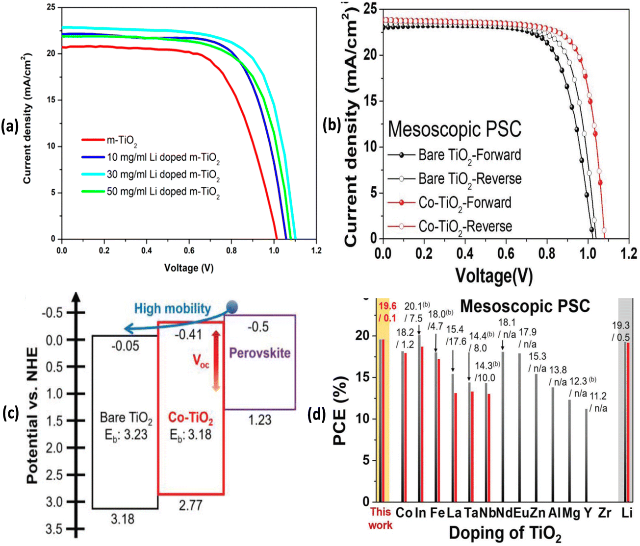 | ||
| Fig. 3 (a) J–V characteristics of PSCs fabricated on undoped mp-TiO2 and variably Li doped mp-TiO2 substrates. (b) J–V curves of Co-doped TiO2 based mp-PSCs in the forward and reverse scan directions for hysteresis characterization. (c) Schematic energy band diagram of Co-doped TiO2 based mp-PSCs. Reprinted with permission from ref. 47. Copyright 2018 John Wiley and Sons. (d) Performance of mp-PSCs with a compact TiO2 layer doped with various elements under a base mp-TiO2 layer. Reprinted with permission from ref. 53. Copyright 2019 American Chemical Society. | ||
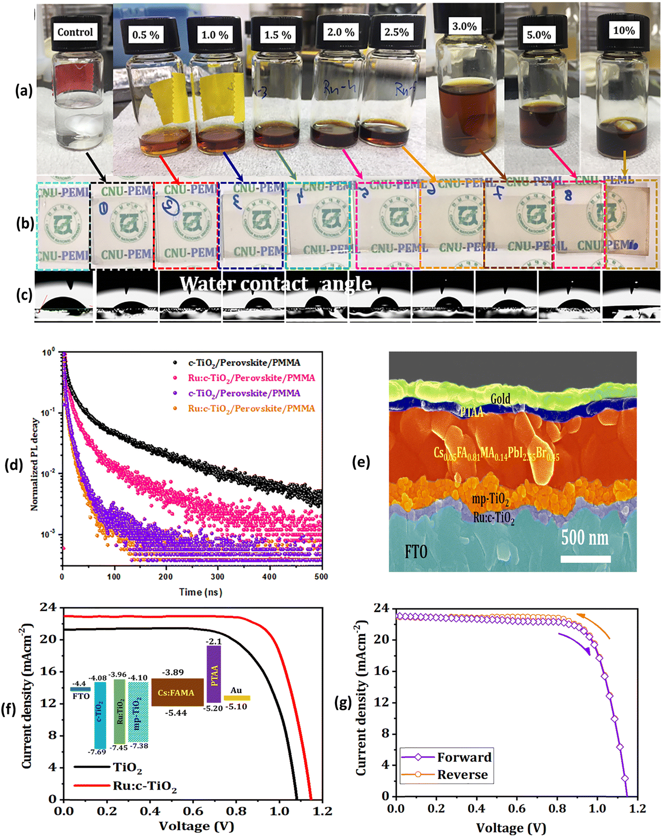 | ||
| Fig. 4 (a) Photographs of the TiO2 precursor solutions with different Ru-dopant concentration. (b) Optical images of the deposited electrodes. (c) Water contact angles. (d) Time-resolved PL (TRPL) measurements based on the triple cation perovskite Cs0.05FA0.81MA0.14PbI2.55Br0.45 on TiO2 and Ru-doped TiO2. (e) Cross-sectional micrograph of the 1.5% Ru:TiO2/mp-TiO2 ETL-based PSC. (f) J–V curves of triple cation perovskite based PSCs deposited onto mp-TiO2/Ru:TiO2 ETL (inset shows the energy-level diagram of the different ETLs used herein). (f) Forward and reverse sweep of the 1.5% Ru-doped TiO2 devices showing negligible hysteresis. Reprinted with permission from ref. 60. Copyright 2021 John Wiley and Sons. | ||
Another viable approach to control TiO2 electronic properties and morphology is by direct growth on alternative substrates such as graphene. This process led for example, in the case of TiO2 NPs, to an intimate interfacial contact and a high quality interface with faster electron extraction which contributed to a enhanced PCE of 15.3% for MAPbI3−xClx cells.66 Furthermore, control and optimization of mp structures can also be obtained by varying the structures and amount of templating polymers (so called soft polymer template engineering technique)67 in order to induce perovskite crystallization, increase grain size and light harvesting as, notably, TiO2 NPs can be densely agglomerated in the scaffold layer thus inhibiting the penetration of a perovskite solution. Alternatively, TiO2 NPs in the highly active but much less explored TiO2-B crystal phase with a narrower band gap (3.09 eV) and longtime stability were recently incorporated in mp-PSCs delivering a high PCE of 18.83% due to the favorable energy level alignment, the fast electron transport and the suppressed recombination at the high crystallinity perovskite/TiO2 interface.68
Despite the successful use of TiO2 in various forms as ETL in mp-PSCs, undesirable recombination losses at the TiO2/perovskite layer interface result in deterioration of device performance. Alternative to doping, interface modification of mp-TiO2 upon introducing an ultrathin passivation layer between the ETL and the perovskite absorber is an efficient, versatile, approach to improve electron transport and thus mp-PSC performance. TiO2 NRs69 and NPs70 have been modified by atomic layer deposition (ALD) of TiO2 which acted as passivation layer of mp ETL in mp-PSCs suppressing charge recombination and enhancing device efficiency. Insulating materials such as MgO,71 Y2O3,72 ZrO2,73 La2O374 and Ta2O575 have also been used as ultrathin (<5 nm, typically 1–2 nm) surface modification and highly effective passivation layers of TiO2 in mp-PSCs. Similarly, Liang et al. inserted a ultrathin Al2O3 interlayer at the mp TiO2/perovskite interface demonstrating an increase in the mp-PSC performance and reduction of J–V hysteresis along with improved device stability due to the decrease of interfacial charge recombination and improved charge transport.76 A delicate interconnected mixture comprising Al2O3 and nanocrystalline TiO2 was also found to be able to tune surface passivation and electron extraction characteristics in mp-PSCs, dependent on the Al2O3 concentration.77 A TiO2/Al2O3 bilayer as the mp scaffold significantly reduced the degradation of the infiltrated perovskite by protecting it from moisture. As a result, it delivered a high PCE of 16.84% which retained 82% of its value after 2000 h storage in ambient air without any optical losses.78
In a different approach, semiconducting GQDs were used as passivation layer in TiO2 based mp-PSC facilitating electron extraction from the perovskite layer to the TiO2 ETL and thus increasing PCE.79 GQDs (<5 nm) decorated on the TiO2 surface led to a more effective interfacial electron transport and extraction which synergistically led to an optimized PCE of 20.45%.80 Incorporation of highly conductive nanocarbon materials, such as graphene and one-dimensional (1D) carbon nanotubes into mp-TiO2 was proposed as an alternative, to direct doping, method to improve electron transport in mp-TiO2.81 For example, TiO2/reduced graphene oxide (RGO) hybrids with an optimal RGO content of 0.2 wt% which were synthesized via an in situ solvothermal process enhanced electron lifetime and recombination resistance resulting in improved electron transport and a 22% higher PCE.82 Single-walled carbon nanotubes (SWCNTs) into the mp-TiO2 also provided an ultrafast electron transport pathway and favorably shifted its CB minimum (i.e. increase the CB minimum) leading to a PCE of 16.11% (compared to 13.53% for the SWCNT-free device) with reduced hysteresis and an enhanced light and long-term stability.83 Another highly innovative strategy involved the incorporation of an optimized amount of colloidal stable, chemically inert, low-cost, Ge NPs with a high refractive index onto mp-TiO2 to regulate perovskite MAPbI3 crystal growth (more specifically, increasing crystal size), decrease the number of the GBs, enhance MAPBI3 electron mobility by a factor of 5 and, thus, promote electron transport at the perovskite/mp-TiO2 interface, resulting in an average PCE of 18.59% (best PCE of 19.6%).84 The influence of other semiconducting materials such as titanium nitride (TiN)85 and zinc sulfide (ZnS)86 as ultrathin buffer layers with an optimum thickness of 1.8 nm deposited on mp-TiO2 by ALD on the performance of mp-PSCs was investigated by Chavan et al. It was shown that both mp-TiO2/TiN and ZnS as a modified ETL significantly improved the optical and morphological properties of the perovskite absorber, while also reduced interfacial charge recombination losses and improved electron extraction resulting in high PCE values of 19.38% and 19.10% with negligible hysteresis.
Alternatively, various organic materials have been used as TiO2 modifiers inserted between the ETL and perovskite layer in mp-PSCs facilitating perovskite crystal growth, passivating interfacial traps and enhancing the device performance. Organic monolayers such as amino acids,87 thiols,88 4-aminobenzoic acid,89 alkylphosphonic acid-ω-ammonium chlorides90 and fullerene derivatives91 as well as Brønsted and other acids such as p-toluenesulfonic acid (p-TA)92 and various alkyl chain length SAMs of phosphonic acids with different terminal groups93 reduced the undesirable surface or GB defects of perovskite appeared during the perovskite film formation as well as passivated TiO2 trap states leading to improved mp-PSCs efficiency, as well as, long-term stability. In particular, change of the alkyl chain length and/or the functional group of the investigated SAM phosphonic acids resulted in a modulation of the TiO2 workfunction and the tunneling barrier/distance. Notably, for iodo-terminated molecules, a longer spacer group led to a lower JSC and FF as a result of the increased barrier/distance for electron tunneling whereas the shortest spacer length increased PCE by ∼30%, compared to pristine TiO2. However, no clear correlation with the modified TiO2 workfunction could be established. Post treatment modification of TiO2 has also been exploited to enhance electron transport, passivate defect states, improve interfacial contact and overcome undesirable interfacial recombination. A representative example is TiCl4 which largely improved TiO2 NP interconnection and the electronic percolation of adjacent NPs, decreased the density of surface trap states and recombination losses at the TiO2/perovskite and enhanced, by an order of magnitude, the bulk electron mobility94 leading to a PCE up to 17.4% compared with 14.1% for pristine TiO2.95 Monoethanolamine (MEA) treatment also improved interfacial energy level alignment, enhanced electron extraction while simultaneously passivated uncoordinated Pb defects on the perovskite interface. These synergistic effects resulted in improved PCE and a remarkable stability under continuous illumination in air.96 Moreover, mixed solvent treatment with an optimized ratio of γ-butylactone and dimethyl sulfoxide resulted in improved wetting of the mp-TiO2, a smoother perovskite layer formation with fewer pinholes and increased grain size combined with passivated GBs. As a result, suppressed carrier recombination and increased electron extraction were obtained leading to an enhnanced PCE of 18.72% compared to 15.21% for the untreated cells.97 Alternatively, TiO2 surface activation upon deep UV light (λ = 254 nm) irradiation was proposed as a feasible strategy to improve its surface wetting properties and facilitate growth of a denser perovskite film with a reduced number of pinholes and consequently with an improved cell PCE.98 UV light was also effective in removing organic binders from TiO2 resulting in a stabilized efficiency of 18.2%.99
Note that the incorporation of a thin compact TiO2 layer between the fluorine-doped tin oxide (FTO) and the mp-TiO2 layer is typically employed in order to further enhance electron transfer and, most importantly, avoid carrier recombination losses with FTO and eliminate carrier shunting paths in mp-PSCs. A similar PCE of ∼18% was reliably achieved at an optimized 230 nm mp-TiO2 layer as well as a compact TiO2 layer in a large equivalent thickness ranging from sub-nanometer to 30 nm.100 A critical compact TiO2 layer thickness of 20–30 nm was found to be optimal for best device performance101 while, obviously, film porosity was also found to play a crucial role in efficient perovskite infiltration for enhanced PCE.102 Similarly, fabrication of a consecutive compact and mp TiO2 film with a dense bottom area and a top mp area with large macropores promoted perovskite infiltration, facilitated electron transport and decreased charge recombination.103 Remarkably, incorporation of both low temperature, high quality, virtually pinhole-free compact combined with mp TiO2 layers, deposited using spray pyrolysis and ALD, respectively, resulted in outstanding PCEs demonstrated under both outdoor and indoor illumination conditions i.e. PCE = 15.9% under the AM 1.5 Spectrum and PCE = 24–25.4% under indoor lighting.104
Another electron transport material used widely in mp-PSCs is zinc oxide (ZnO) due to its high transparency (bandgap ∼3.3 eV), a higher bulk electron mobility (>200 cm2 V−1 s−1), compared to TiO2, a favorable CB minimum (∼4.2 eV) and a considerably lower crystallization temperature combined with its ability to create various nanostructures. Bi et al. used for the first time ZnO NRs as ETLs in mp-PSCs.105 Although the mp-PSCs based on ZnO NRs showed lower PCE values than those with TiO2 as ETL due to increased charge recombination losses, the devices exhibited good long-term stability. Park's group investigated the influence of the ZnO seed layer on the growth of the ZnO NRs, as well as, the effect of the size of the prepared ZnO NRs on the mp-PSCs performance.106 Three different coating solutions, including clear solution, colloidal solution and nanopowder solution, were studied for the formation of the ZnO seed layer exhibiting various photovoltaic parameters. In particular, the highest VOC improvement was recorded for the mp-PSC with the ZnO NRs grown on the colloidal seed layer exhibiting also increased recombination resistance as revealed from impedance spectroscopic measurements. Moreover, the diameter and length of the ZnO NRs played a critical role in the performance of the ZnO NRs-based mp-PSC with the optimized mp-PSC based on 1 μm ZnO nanorod-ETL reaching a PCE value of 11.13%. Recently, Yun et al. developed well-ordered ZnO NRs with controllable lengths and studied the effect of the ZnO nanorod length on the performance and stability of mp-PSCs.107 It was demonstrated that the optimized length of the NRs at 400 nm facilitated the infiltration of the perovskite absorber into the ETL and improved the perovskite crystallinity, resulting in enhanced electron transport and thus improved PCE of 14.23%. This approach has also been applied in lead free Cs2SnI6 mp-PSCs where optimization of the nanorod length and pore size to ensure high-loading of the perovskite resulted in moderate but stable PCEs of ∼1%.108 In a different so-called double-layer nanostructured ETL approach, low-temperature hydrothermal synthesis of a double-layered mp nanostructured ZnO film, consisting of a vertically aligned film of nanosheet arrays decorated by horizontally-arranged NRs with improved electron transport was successfully implemented in mp-PSCs.109
As in the case of mp-TiO2, doping and interfacial modification can significantly improve the electron transport properties of ZnO. Dong et al. used Al-doped ZnO to modify ZnO NRs.110 An improvement on mp-PSC performance was demonstrated for the device with the modified ZnO NRs ascribed to the high CB minimum and electron mobility of the Al-doped ZnO facilitating electron transport, while also reducing recombination losses. Furthermore, Mahmood et al. prepared vertically aligned ZnO NRs with TiO2 shell ETLs by a hydrothermal method.111 The mp-PSCs using the core-shell ZnO/TiO2 showed reduce charge recombination along with excellent light-harvesting capability resulting in improved efficiency with low hysteresis. In another study, superaligned ZnO NRs (SAZNRs) were prepared on commercially available AZO seed layers using a low-temperature processing.112 Zhao et al. not only demonstrated the effective use of AZO/SAZNRs as ETLs in mp-PSCs fabricated on rigid and flexible substrates, but also the efficient recycling of the devices by a simple process and re-fabrication of the mp-PSC with slightly reduced performance. The effect of doping combined with surface modification of low-temperature solution-processed ZnO NRs on the mp-PSCs performance was also reported by Mahmood et al.113 The N-doped ZnO NRs (N:ZnO NR) ETL exhibited improved electron transport properties and reduced work function compared to the undoped ZnO nanorods resulting in improved device efficiency. However, a significant increase in device performance from 10% to 16% was obtained when a polyelectrolyte polyethylenimine (PEI) monolayer was used as interfacial modifier of the N-doped ZnO NRs, attributed to the improved infiltration of the perovskite material into the ETL and the favorable work function shift of the PEI-modified N:ZnO NR. Li et al. fabricated mp PbI2 based PSCs using ZnO NRs modified by ALD Al2O3 monolayers.114 High-quality perovskite films with few defects and large grains were prepared on Al2O3-passivated ZnO NRs resulting in reduced recombination losses and a high PCE value of 17.3%. In a recent work, a superior PCE of 20.74% was obtained when PEI-mixed multidoped (B and F) ZnO NCs prepared by a low-temperature solution-processed electrospraying deposition method were applied in mp-PSCs as ETLs.115 In particular, mp pure ZnO, boron-doped (B:ZnO), tantalum-doped (Ta:ZnO), boron and fluorine co-doped (B,F:ZnO), and tantalum and nitrogen co-doped (Ta,N:ZnO) ZnO nanolayers were effectively employed as highly efficient ETLs showing high conductivity, transparency and tunable band gap energy. Remarkably, the position of the CB edge using combination of B and F dopants may be raised up to 0.22 eV compared to pristine ZnO, thus resulting in increased VOC, suppressed carrier recombination and faster electron transport. A further improvement in the performance of hysteresis-free mp-PSCs was reported with the deposition of PEI on top of the multidoped ZnO nanolayers, which reduced the multidoped ZnO work function and trap-assisted charge recombination, resulting in an outstanding PCE value over 20% and representing one of the highest reported efficiencies for mp ZnO-based PSCs. Fig. 5 represents the schematic illustration of PEI-mixed multidoped ZnO film formation, the fabricated PSC structure, the energy level of the corresponding cells, along with the J–V characteristic curves of the champion devices. Furthermore, ZnO surface modification by binding (i.e. grafting) fullerene to create ingeniously designed fullerene-anchored core–shell NPs resulted in a multifunctional ETL that passivated ZnO surface, improved electron extraction and suppressed ion/water diffusion, being part of the first-ever dual-sensitized (i.e. mp ETL and HTL scaffolds incorporated in the same architecture) novel metal-oxide based mp architecture on a NiOx scaffold reaching state of-the-art PCEs of 21.1% and 20.21% for mixed-cation and MAPbI3 PSCs.116
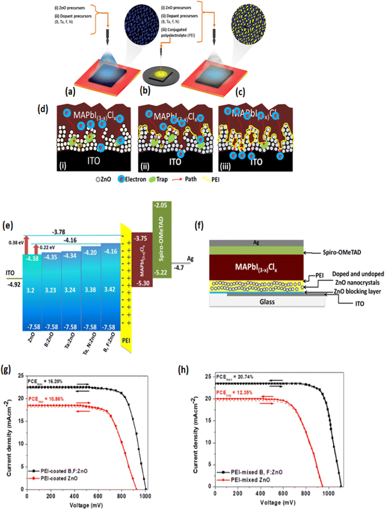 | ||
| Fig. 5 Schematic illustration of low-temperature and fully solution-processed electrospray-deposited (a) pure ZnO and multidoped ZnO NCs (the inset is the magnified view of mp NCs); (b) PEI-coated ZnO and multidoped ZnO nanolayers; and (c) PEI mixed pure ZnO and multidoped ZnO NCs (the inset is the magnified view of PEI-blended NCs). (d)(i)–iii)) Schematic illustration of device architecture based on the above oxide nanolayers showing the electron trapping due to the voids between ZnO NCs. (e) Illustration of device architecture with PEI-coated and PEI-mixed ZnO and doped ZnO nanolayers and (f) energy-level diagram of the corresponding devices with five various types of pure and doped ZnO nanolayers. J–V curves for the champion devices with (g) PEI-coated and (h) PEI-mixed ZnO and B, F:ZnO nanolayers using different sweep directions. Reprinted with permission from ref. 115. Copyright 2018 American Chemical Society. | ||
Nanostructured mesoporous SnO2 is another well-known ETL used in mp-PSCs. SnO2 is a promising ETL due to its high transparency (bandgap > 3.5 eV), its deep CB minimum (∼4.2 eV) leading to a favorable energy level alignment with that of the perovskite absorber and efficient electron extraction, its high bulk electron mobility (∼250 cm2 V−1 s−1), its outstanding UV stability and, importantly, its low temperature processing (comparable to ZnO but lower than TiO2) from solution or sol–gel. Zhu et al. reported the first application of hydrothermally synthesized mp SnO2 as ETL in mp-PSCs.117 Despite the high electron mobility of SnO2, SnO2-based mp-PSCs suffered of strong recombination of the photogenerated charges resulting in poor efficiency. However, treatment of SnO2 with TiCl4 forming a thin TiO2 layer deposited on top of SnO2 significantly improved the device performance. In a similar work, impedance spectroscopic measurements revealed the beneficial TiCl4 treatment of SnO2 since the ultrathin TiO2 layer coated on SnO2 ETL reduced trap states facilitating electron transfer within the mp-PSC.118 Liu et al. developed low-temperature hydrothermal SnO2 nanosheets (NSs) as ETLs and investigated the influence of the prepared ETLs on the stability of mp-PSCs.119 Interestingly, the mp ETL improved photon collection, prevented moisture penetration in the perovskite material which could lead to degradation of the photoactive layer, and enhanced device stability. Moreover, the stability of mp-PSCs using mp-SnO2 under UV light was investigated by Roose et al.120 It was demonstrated that the mp-SnO2 prevented the degradation of the perovskite absorber leading to mechanical and chemical stability of mp-SnO2-based mp-PSCs in comparison with the planar SnO2-based device where the initial PCE was decreasing after 10 h of 1.5AM illumination exposure. The same group also investigated the affect of Al-doped mp-SnO2 on efficiency and UV stability of mp-PSCs.121 Al-doping reduced recombination losses originated by the trap states of mp-SnO2 resulting in higher PCE value of 16.4% compared with the 12.7% efficiency of the undoped ETL-based device. Furthermore, the reduced photocatalytic activity of Al-doped mp-SnO2 was beneficial to device stability, attributed to the wider band gap of m-SnO2 compared to that of mp-TiO2, making mp-SnO2 a promising substitute of TiO2 ETL for efficient and stable mp-PSCs. Similarly, Guo et al. reported highly-efficient mp-PSCs using rare-earth (e.g. lanthanide (Ln)) ions as dopants of mp-SnO2 nanospheres.122 In particular, Y-doped SnO2 based mp-PSCs showed high efficiency of 20.63% without hysteresis, while the device with the undoped ETL exhibited a PCE of 19.01%. This significant improvement in mp-PSC performance was attributed to the improved quality of the perovskite layer forming dense and large crystals favorable to good physical contact, as well as, to the enhanced energy level alignment at the ETL/perovskite absorber interface. Also, Nb5+ n-type doped SnO2 with a deeper CB minimum, reduced defect state density and suppressed interfacial recombination was favorably utilized as ETL to fabricate TiO2 based mp-PSCs with a ∼10% higher PCE (i.e. 13.53% for MAPbI3 employing a 2 mol% optimized doping concentration) compared to that with undoped SnO2 as a result of the enhanced cell photovoltage by 40 mV,123 thus highlighting the multiple functionalities of appropriate dopants in mp metal oxide ETLs such as TiO2. SnO2 or ZnO.
More recently, a two-dimensional SnO2 layer which enhanced the ETL/perovskite interfacial contact area and facilitated electron extraction as well as assisted in the growth of large-sized all inorganic CsPbB3 grains (up to 1.65 μm) and enhanced light-harvesting resulted in a PCE of 9.51% free of hysteresis. Further modification of the interface with graphene QDs led to a champion PCE of 10.34% due to the improved interfacial energy level alignment.124 Alternatively, mp-SnO2 surface modification with a rubidium fluoride (RbF) layer synergistically passivated interfacial traps and enhanced electron extraction leading to a remarkable PCE of 22.72% and maintaining 90% of the initial PCE after 300 h of tracking operation at the cell maximum power point (MPP).125 As in the case of TiO2, the controlled porosity and roughness of mp SnO2 was beneficial to passivate the trap states at the ETL/perovskite absorber interface leading to improved electron collection efficiency as nicely demonstrated by Wang et al.126 To tune the morphology of mp-SnO2, they proposed a low-temperature method where polyethylene glycol (PEG) acting as a pore-forming agent was added to the pristine SnO2 solution followed by the removing of PEG from the forming mp-SnO2 film through a low-temperature process. The performance of mp-PSCs using this mp-SnO2 as ETL was dependent on the PEG volume ratio with the best device exhibiting a high PCE of 20.82% for 6% PEG volume ratio. Moreover, Song et al. applied an emulsion-based bottom-up self-assembly strategy to prepare SnO2 microspheres in combination with an in situ ligand-stripping method forming a high-quality mp SnO2 film.127 The prepared mp-SnO2 ETL showed better electron transport properties than the planar SnO2 resulted in highly-efficient mp-PSCs with PCE of 21.35%. Using a surfactant-free solvothermal method, Fan et al. synthesized a series of high-quality monodispersed SnO2 microspheres with high surface area, diameters between 75 and 200 nm and enhanced crystallinity and employed them by spay-coating as ETLs to obtain a high PCE of 16.85% in mixed-cation PSCs which was further improved to 17.08% by adding GQDs into the ETL to enhance perovskite crystallinity, reduce recombination and enhance electron transport as a more favorable energy level alignment at the SnO2/perovskite interface was achieved (i.e. a negative shift of the SnO2:GQDs CB minimum under illumination).128 Notably, a bilayer NP-based mp-SnO2 upon deposition of two consecutive mp layers by anodizing a metallic Sn film in a NaOH solution on FTO under ambient conditions enabled very recently not only complete coverage of ITO but also excellent control of the film morphology by optimizing the anodization voltage and time (with a constant solution concentration) resulting in a 27% improvement of a MAPbI3-based cell PCE as demonstrated by Ullah et al.129
Combining TiO2 and SnO2 in a mesoscopic oxide double ETL “complimentary” approach was first proposed by Tavacoli et al. who proposed a TiO2 NP scaffold covered by a thin film of SnO2 either in amorphous, crystalline or nanocrystalline form.130 The amorphous SnO2 coated TiO2 was found to be the optimum ETL due to the larger band gap of the amorphous SnO2 (compared to the crystalline/nanocrystalline forms) leading to an upshift of the CB minimum and an excellent interfacial alignment with those of the triple cation perovskite and the TiO2 scaffold. As a result, faster electron extraction and reduced carrier recombination were obtained leading not only to a remarkable 0.17 V gain in the VOC and a 20.4% PCE (i.e. 6% higher than the cell with the bare mp-TiO2) but also to a drastically improved UV stability (i.e. only a 3% PCE reduction) of triple-cation PSCs after 60 h UV exposure (see Fig. 6).
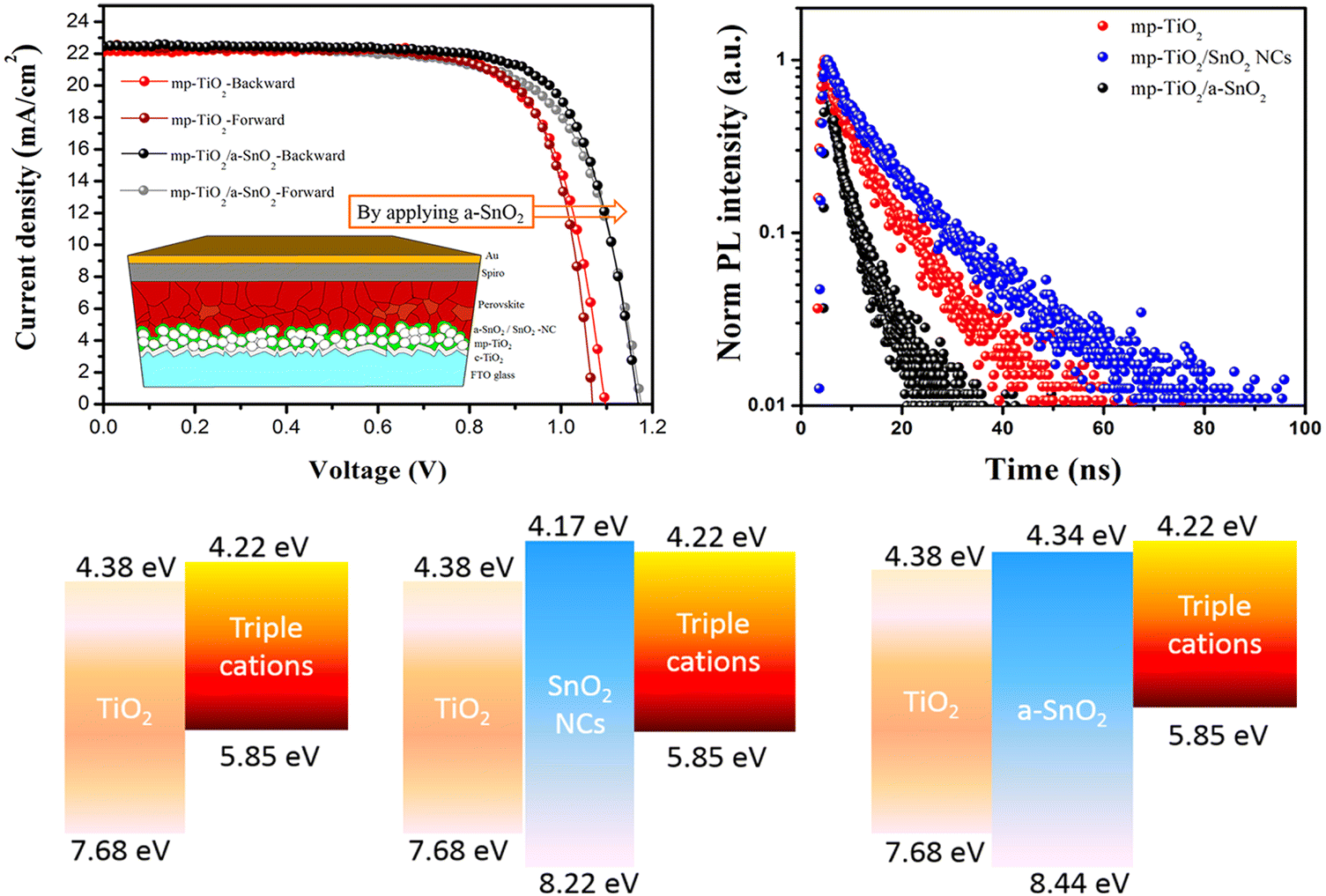 | ||
| Fig. 6 J–V curves of the mp-PSCs on mp-TiO2, mp-TiO2/SnO2- and mp-TiO2/a-SnO2 (inset is the mp oxide double layer based n–i–p device structure) (top left), time-resolved PL (TRPL) curves of perovskite films on the different mp metal oxides mp-TiO2 (top right) and schematics of energy band alignment at the perovskite/mp-metal oxide interfaces (bottom). Reprinted with permission from ref. 130. Copyright 2018 American Chemical Society. | ||
Besides TiO2, ZnO, and SnO2, other n-type transition metal oxides such as tungsten oxide (WO3) have also been explored as an ETL in mp-PSCs. Mahmood et al. prepared WO3 with different nanostructures including NRs, NPs, and NSs and demonstrated that the introduction of the latter as ETL significantly improved the mp-PSC performance in comparison with the devices based on the other two WO3 nanostructures due to the improved contact at the ETL/perovskite absorber along with the good perovskite film formation resulting in fast electron transfer from the photoactive layer towards the electrode.131 Furthermore, ternary oxide materials have been studied as substitutes of mp-TiO2 ETL. Chung et al. reported recently the successful incorporation of another n-type semiconductor, namely BaSnO3 (BSO), as the mp ETL in PSCs, demonstrating not only a remarkable and among the highest PCEs over 22% among non-TiO2 based devices but also exceeding even those efficiencies (typically >21%) that can be obtained with Li-doped TiO2.132 A better physical contact between the BSO and the perovskite layer than that with the TiO2 ETL was observed which complements its high electron mobility and its appropriate CB minimum to facilitate ultrafast electron transport and extraction and thus to improve JSC and FF. Moreover, under high humidity conditions (40% relative humidity), devices with mp BSO exhibited much higher stability than Li-doped TiO2 ones as the Li hydroscopic nature is deleterious for device stability in humid air whereas BSO is superior in terms of moisture stability. Another ternary metal oxide, SrTiO3, was investigated as ETL in mp-PSCs by Bera et al.133 It was demonstrated that SrTiO3 enhanced surface coverage of the perovskite absorber, while also exhibited favorable energy level alignment at the ETL/perovskite interface, increasing the shunt resistance and hence enhancing device performance, as compared with TiO2-based mp-PSCs. Also, improved electron transfer and collection attributed to the well-matched energy levels between the mp ternary metal oxide ETL and the perovskite layer were recently demonstrated by Guo et al.134 In particular, mp-PSCs based on low temperature solution-processed mp zinc titanate ZnTiO3 (ZTO) exhibited not only improved efficiency of 20.5%, but also excellent long-term stability, along with good reproducibility. Apart from its intrinsic superior photostability (i.e. is free of photoshunts) which is ideal for cell UV stability, ZTO assisted in perovskite crystal growth by increasing the number of nucleation sites for film formation, reduced trap state density upon deposition on SnO2 as well as improved its wettability whereas its appropriate CB edge energy facilitated electron transfer at the interface with perovskite. Moreover, Oh et al. used for the first time the mp Zn2SnO4 (ZSO) as ETL in mp-PSCs135 while Bera et al. showed that ZSO improved the crystal formation of the perovskite layer deposited on top of it combined with an enhanced electron transport capability.136 Recently, Zheng et al. used ZSO single crystal mp layer of controllable particle size and morphology in mp-PSCs, demonstrating a high efficiency of 18.32% attributed to the high JSC, and good stability in air with 20% humidity for 15 days (without encapsulation).137 In a new concept, recently proposed by Chung et al., a low temperature processed energy-level engineered porous planar bi-layered ETL inspired by a mp structure which employed a model combination of SnO2 NPs with 2 nm-size and ZSO NPs with 20 nm-size as a compact layer achieved a PCE value of 20.7% and a corresponding 19.9% value on a flexible substrate by succeeding in maximising electron collection and minimizing carrier recombination.138
Summaring the major previously discussed findings in mp-ETLs, it is evident that although anatase mp-TiO2 typically comprising of ∼30 nm NPs is still the most common ETL used for high efficiency (>20%) n–i–p mp-PSCs major efforts have been undertaken to improve further both electron transport and collection efficiency and enhance pore-filling and crystallization of the perovskie in the mp scaffold by following different approaches and strategies. Notably, various metal oxide nanostructures (e.g. NRs, NWs, NTs, NSs) have been carefully designed and incorporated in mp-ETL based PSCs. More specifically, 1D nanostructures such as metal oxide NRs, NWs and NTs (either in their pristine state or with embedded, for example, carbon nanotubes) provide a direct, highly efficient, “highway” channel for fast, barrier-free, photogenerated electron transport while they also allow better pore filling and infiltration of the perovskite due to their open and regular pore structure. Furhthermore, 2D nanosheets have been shown to allow even better, compared to their 1D counterparts, perovskite infiltration, thus reducing carrier recombination while fast, direct, electron transport can also be achieved. 3D nanostructures have the additional advantage of increasing light harvesting by optical scattering.
Elemental doping of the mp metal oxides is another viable and simple approach to enhance the mp-ETL optoelectronic properties, favorably engineer the interfacial energy level alignment by appropriate band gap engineering and improve perovskite crystallinity and mp scaffold infiltration. In particular, Li doping favorably upshifted the CB edge of the metal oxide resulting in more efficient interfacial electron transport but suppressed interfacial carrier recombination upon reducing surface electron trap density while, at the same time, it boosted mp metal oxide electronic conductivity and mobility. Similar effects were observed upon doping with Mg, Sn, Nd or Y or alkali metals which lowered the modified metal oxide workfunction and passivated surface defects. A more significant electron conductivity increase and an associated stronger enhancement of electron transport and extraction was observed upon doping with Nb or Ta which downshifted the CB minimum. However, it is critical to keep dopant concentrations to small amounts (up to a few % by wt) as heavy doping rapidly deteriotated device performance due to the increasingly difficult electron transport in heavily-doped mp metal oxides. Doping in some cases promoted the formation of aligned metal oxide NS arrays (e.g. Y doped SnO2) that facilitated perovskite infiltration and enhanced interfacial contact with the perovskite.
A different, alternative to doping, promising strategy is surface modification. In this case, surface traps can be effectively passivated, charge recombination may be largely suppressed and the interfacial energy level alignment may be further optimized. Various insulating metal oxides, SAMs, organic molecules, chlorides and acids have been found to modify the mp metal oxide surface and its properties by either favorably shifting the CB edge and/or passivating oxide surface traps. Furthermore, some molecules with appropriate functional groups have been found to be highly effective in passivating positively and negatively charged ionic defects in the perovskite, reducing its grain boundary density and enhancing its crystallinity and mp scaffold infiltration. Post-treatment of mp metal oxides is also a feasible tool to enhance interaction with the perovskite and passivate surface traps. Post treatment including laser sintering, annealing and UV-ozone or plasma treatment could have multiple, different, functionalities including modulating the oxide work function, suppressing surface defects and forming a more uniform, pinhole-free perovskite film.
More advanced strategies include the development of structured bilayered metal oxide architectures, metal oxide nanocomposites or hybrid composites with carbon-based nanomaterials such as graphene QDs and carbon dots or noble metals such as Al or Ag NPs as well as novel ternary (or quaternary) metal oxides. For example, noble metal NPs decorating the mp metal oxide prompted optical effects by enhancing light absorption owing to the near field enhancement associated with the metal-induced localized surface plasmon resonance and an enhanced charge transport. On the other hand, nanocomposites with graphene QDs enhanced electron conductivity and decreased the metal oxide workfunction, thus facilitating electron transfer and extraction.
Finally, with regard to the most employed mp-ETL modification strategy implemented by the community to fabricate highly efficient (>21%) n–i–p mp PSCs, we wish to note that TiO2 doping with Li salts is one of the most promising approaches to improve electron transport and has appropriately become the gold standard to obtain superior PCE in n–i–p mp PSCs. However, despite its excellent promise, serious stability concerns have been recently raised due to the very high hydroscopicity of the Li dopant which results in the formation of a deleterious thin Li oxide layer and the high Li ion reactivity with moisture, thus preventing the possibility for commercialization of this technology. It now becomes increasingly clear that the ideal candidate may be, alternative to TiO2, mp ternary metal oxides with exceptional optoelectronic properties that combine high photostability under continuous illumination and superior UV, thermal and chemical stability in humid air.
3.2 Planar ETLs employed in p–i–n mp-PSCs
With regards to planar ETLs which can be incorporated in p–i–n mp-PSCs, so far there have been only a handful of materials used in this device architecture. The work horse initially employed was C60 whereas its soluble derivative PC61BM is gaining more interest in recent years. Typically, a single planar ETL either a thermally deposited C60 layer139 or a solution-processed P61CBM layer140–142 topped on various perovskite layers has been utilized with a thickness ranging approximately between 20 and 50 nm resulting in efficient, trap-free, electron transport and extraction at the cathode electrode. Enhanced and more stable efficiencies could be utilized upon depositing an appropriate charge selective overlayer on C60 or P61CBM to create a blayer ETL in order to enhance hole blocking and suppressed undesired charge recombination. A typical organic small molecule employed therein is an ultrathin bathocuproine (BCP) layer, thermally deposited either on C60139 or on PC61BM.143–148 Notably, other novel small molecules employed recently instead of BCP in the double-layered ETL configuration include a C60 bisadduct (bis-C60) as a surfactant149 and a zirconium acetylacetonate (ZrAcac) molecule,150 both sequentially coated as very thin layers from solution on isopropyl alcohol and methanol, respectively, onto the PC61BM underlayer. As a result, an ideal cascade energy level alignment could be obtained for electron transfer and extraction with reduced interfacial accumulation combined with a smooth film surface which resulted in significantly improved PCE and stability of the fabricated PSCs. Alternatively, a ZnO NC overlayer spin-coated from a colloidal NP solution on top of PC61BM was also found to be highly effective in facilitating electron transport and collection to the cathode in the inverted mp architecture.151In Table 1, a summary on high performance mp-PSCs with a n–i–p architecture based on representative materials employed as the ETL is provided.
| mp ETL | Nanostructure or pore size | Fabrication method | Post-treatment or Modification type | mp-PSC structure | PCE (%) | PCE improvement vs. referencea (%) | Ref. |
|---|---|---|---|---|---|---|---|
| a The corresponding value is not provided. | |||||||
| TiO2 | 20 nm NPs with optimum 40 nm pore size (upon employing submicron sized (85 nm) carbon spheres as a template) | Hydrothermal method | — | FTO/TiO2/MAPbI3(Cl)/Spiro-OMeTAD/Ag | 15.60 | 45 | 32 |
| PS-TiO2 | 20 nm NPs (upon employing sub-micron sized (200 nm) polystyrene (PS) microspheres as a sacrificial template) | Hydrothermal method | TiCl4 aqueous solution | FTO/PS-TiO2/MAPbI3(Cl)/Spiro-OMeTAD/Au | 6.93 | 10 | 33 |
| Mesoscopic inverse opal TiO2 film | 35 nm NPs/pore size < 100 nm | Employing a PS colloidal opal crystal template followed by chemical vapor deposition of TiO2 | — | FTO/opal TiO2/MAPbI3/PTAA/Au | 17.10 | 9 | 34 |
| 3D TiO2 NWs | 3.3 μm NW length | Hydrothermal method | — | FTO/TiO2 NWs/MAPbI3/Spiro-OMeTAD/Au | 13.97 | 23 | 36 |
| 3D orchid-like TiO2 NWs:SiO2 coated Ag NPs composites | 400 nm length NWs | Hydrothermal method | — | FTO/TiO2 NWs:SiO2 coated Ag NPs/MAPbI3−xClx/Spiro-OMeTAD/Au | 15.09 | 24 | 37 |
| 1D TiO2 nanopyramid (NPy) arrays | 285 nm NPy length | Hydrothermal method | — | FTO/TiO2 NPys/MAPbI3−xBrx/Spiro-OMeTAD/Au | 22.48 | 38 | |
| 1D TiO2 nanorod (NR) arrays | 298 nm NRs length | Solvothermal method | — | FTO/TiO2 NRs/MAPbI3−xBrx/Spiro-OMeTAD/AgAl | 17.03 | 18 | 39 |
| TiO2 microspheres | 150 nm size | Emulsion-based self-assembly | — | FTO/TiO2 microspheres/Cs0.05 (MA0.15 FA0.85)0.95Pb(I0.85Br0.15)3/Spiro-OMeTAD/Au | 19.27 | 40 | |
| Hollow 3D TiO2 sub-microspheres | 15–45 nm pore size | Spin coating | — | FTO/TiO2 sub-microspheres/MAPbI3/Spiro-OMeTAD/Au | 18.01 | 28 | 41 |
| Ti–Zn–O hollow nanospheres | <100 nm | Solution process followed by sintering and spin coating | Cation (Zn2+) exchanging step | FTO/Ti–Zn–O nanospheres/FAMAPbI3−xBrx/Spiro-OMeTAD/Au | 16.39 | 9 | 42 |
| CsBr modified TiO2 beads | 40 nm NPs endowed with pores of a few nanometere diameter | Premixing, spin coating and sintering at 450 °C | CsB surface modification | FTO/Cs doped TiO2/Rb:Cs:FA0.95MA0.05PbI3/Spiro-OMeTAD/Au | 21.00 | — | 43 |
| TiO2 | ∼30 nm NPs | Spin coating | Intense pulse laser sintering | ITO/TiO2 (IPL)/MAPbI3/Spiro-OMeTAD/Au | 16.70 | 5 | 45 |
| Al doped TiO2 | ∼30 nm NPs | Sol gel | Al doping | FTO/Al doped TiO2/MAPbI3//Spiro-OMeTAD/Au | 14.05 | 22 | 46 |
| Co doped TiO2 | ∼30 nm NPs | Dip coating and rapid post annealing | Co doping | FTO/Co doped TiO2/(FAPbI3)0.85MAPbBr3)0.15/Spiro-OMeTAD/Au | 20.00 | 8 | 47 |
| Zn doped TiO2 | 17.5 nm NPs | Sol gel and hydrothermal method | Zn doping | FTO/Zn doped TiO2/MAPbI3//Spiro-OMeTAD/Ag | 16.80 | 28 | 49 |
| Li doped hierarchical TiO2 nanostructures | 11 nm pore size | Spin coating and sintering | Li doping | FTO/Li doped TiO2/MAPbI3//Spiro-OMeTAD/AgAl | 18.25 | 17 | 52 |
| Li doped TiO2 | ∼30 nm NPs | Spin coating | Li doping | FTO/Li doped TiO2/MAPbI3/Spiro-OMeTAD/Au | 17.59 | 29 | 53 |
| Li2CO3 doped TiO2 | 50 nm NPs | Spin coating | Li2CO3 doping | FTO/Li2CO3 doped TiO2/FAPbI3/Spiro-OMeTAD/Au | 24.70 | 14 | 55 |
| Zr/N codoped TiO2 NR arrays | 460 nm Zr/N codoped TiO2 NRs length | Hydrothermal method | Zr/N codoping | FTO/Zr/N codoped TiO2 NRs/MAPbI3/Spiro-OMeTAD/Au | 12.60 | 32 | 58 |
| Ru doped TiO2 | Spin coating | Ru doping | FTO/Ru doped TiO2/Cs0.05FA0.81MA0.14PbI2.55Br0.45/PTAA/Au | 20.87 | 28 | 60 | |
| Ag doped TiO2 | 15 nm NPs | Solution and centrifugation | Ag doping | FTO/Ag doped TiO2/MAPbI3/Spiro-OMeTAD/Ag | 16.50 | 14 | 61 |
| Graphene QDs (GQDs) doped TiO2 | Spin coating | Graphene QDs doping | FTO/GQDs doped TiO2/Cs0.05(FA0.17MA0.83)0.95 Pb(I0.83Br0.17)3/Spiro-OMeTAD/Au | 14.36 | 55 | 63 | |
| Hydrogenated TiO2 (H-TiO2) NCs | 25 nm H-TiO2 NCs with length of 200 nm | Sol–gel hydrothermal method | — | FTO/H-TiO2/MAPbI3//Spiro-OMeTAD/Au | 13.22 | 21 | 64 |
| 4-Chlorobenzoic acid (CIBA)doped TiO2 | 49 nm NPs | Spin coating | Doping with CIBA | FTO/CIBA doped TiO2/FAMAPbI3−xBrx/Spiro-OMeTAD/Au | 20.22 | 11 | 65 |
| TiO2/graphene nanocomposites | 10 nm NPs | Laser pyrolysis | Nanocomposites with graphene | FTO/TiO2/Graphene/MAPbI3−xClx/Spiro-OMeTAD/Au | 15.30 | 11 | 66 |
| TiO2 B phase (TiO2-B) | TiO2-B NPs | Spin coating | — | FTO/TiO2-B/(FAPbI3)1-x(MAPbBrx)x/Spiro-OMeTAD/Au | 18.83 | 13 | 68 |
| Graphene QD surface decorated TiO2 | 25 nm NPs | Spin coating | Graphene QD surface decoration | FTO/Graphene QD decorated TiO2/FAMAPbI3−xBrx/Spiro-OMeTAD/Au | 20.45 | 10 | 80 |
| TiO2/reduced graphen oxides (RGO) hybrids | TiO2:RGO nanocomposites | Solvothermal process | Modification with RGO | FTO/TiO2:RGO/MAPbI3−xClx/GO/CuBuPc/Au | 15.9 | 22 | 82 |
| Single wall carbon nanotube (SWNT) embedded TiO2 | NPs | Spin coating | SWNT addition into TiO2 | FTO/TiO2:SWNT/MAPbI3/Spiro-OMeTAD/Au | 16.11 | 19 | 83 |
| Colloidal Ge NPs modified TiO2 | 100 nm Ge NPs | Spin coating | Ge NPs modification | FTO/Ge NPs modified TiO2/MAPbI3/Spiro-OMeTAD/AgAl | 18.59 | 14 | 84 |
| Ultrathin TiN (1.9 nm) modified TiO2 | ∼30 nm TiO2 NPs | ALD | TiN modification as buffer layer on TiO2 | FTO/TiN modified TiO2/FA0.83MA0.17Pb(I0.83Br0.17)3/Spiro-OMeTAD/Au | 19.0 | 14 | 85 |
| Ultrathin ZnS (1.8 nm) modified TiO2 | ∼30 nm TiO2 NPs | ALD | ZnS modification as buffer layer on TiO2 | FTO/ZnS modified TiO2/(FAPbI3)0.85 (MAPbBr3) 0.15/PTAA/Au | 18.80 | 8 | 86 |
| p-TA modified TiO2 | ∼30 nm TiO2 NPs | Spin coating | p-TA modification of TiO2 | FTO/p-TA modified TiO2/MAPbI3/PTAA/Au | 19.29 | 8 | 92 |
| Phosphonicacids modified TiO2 | ∼30 nm TiO2 NPs | Immersing in solution | Phosphonic acids modification of TiO2 | FTO/Phosphonic acids modified TiO2/MAPbI3/Spiro-OMeTAD/Ag | 16.09 | 17 | 93 |
| TiCl4 treated TiO2 | 10–50 nm NPs | Spin coating | Immersion in TiCl4 aqueous solution | FTO/TiCl4 modified TiO2/MAPbI3/Spiro-OMeTAD/Au | 17.40 | 23 | 95 |
| TiO2 | ∼30 nm NPs | Spin coating | UV treatment at 254 nm | FTO/UV-treated TiO2/MAPbI3/Spiro-OMeTAD/Au | 9.3 | 22 | 98 |
| Multidoped (B, F) PEI mixed ZnO NCs | Solution processed electrospraying | Multidoping of ZnO with B and F and mixing with PEI | FTO/PEI doped ZnO NCs/MAPbIxCl3−x/Spiro-OMeTAD/Au | 20.74 | 61 | 115 | |
| Fullerene-anchored ZnO NPs (Fa-ZnO) | 5 nm Fa-ZnO NPs | Spin coating | Anchoring ZnO NPs with fullerene nano-shells | FTO/NiOx/FA0.85MA0.15PbI2.55Br0.45/Fa-ZnO/Ag | 21.11 | 9 | 116 |
| Y doped SnO2 nanospheres | Pore size 13.8 nm | In solution followed by spin coating | Y doping | FTO/Y doped SnO2 nanospheres/Cs:FA:MAPbIxBr3−x/Spiro-OMeTAD/Au | 20.63 | 9 | 122 |
| SnO2 NR self-assembled microspheres | <100 nm | Emulsion-based self-assembly | — | FTO/SnO2 NR self-assembled microspheres/Cs:FA:Cs0.05(MA0.15FA0.85)0.95Pb(I0.85Br0.15)3/Spiro-OMeTAD/Au | 21.35 | 127 | |
| SnO2 microspheres with added GQDs | 75 nm size | Solvothermal method | Addition of graphene QDs into the SnO2 microspheres | FTO/SnO2 microspheres:GQDs/(FAPbI3)0.85 (MAPbBr3)0.15/Spiro-OMeTAD/Au | 17.08 | 30 | 128 |
| TiO2 NPsamophous SnO2 | ∼20 nm TiO2 NPs covered by amorphous SnO2 | Spin coating | Covering TiO2 NPs with amorphous SnO2- | FTO/TiO2 NPs/SnO2/Cs(FAPbI3)0.87(MAPbBr3)0.13/Spiro-OMeTAD/Au | 20.40 | 7 | 130 |
| WO3 NS arrays | ∼500 nm length and ∼100 nm width WO3 NSs | Hydrothermal growth | TiCl4 treatment for an ultrathin TiO2 overlayer | FTO/WO3 NSs/TiO2/MAPbI3/Spiro-OMeTAD/Ag | 11.24 | 131 | |
| BaSnO3 (BSO) NPs | Spin coating | — | FTO/BSO/(FAPbI3)0.93(MAPbBr3)0.07/Spiro-OMeTAD/Au | 21.30 | 132 | ||
| SrTiO3 NPs | <100 nm | Spin coating | — | FTO/SrTiO3/MAPbI3−xClx/Spiro-OMeTAD/Au | 7.55 | 5 | 133 |
| ZnTiO3 (ZTO) | ∼15 nm ZTO NPs | Sol gel and spin coating | — | FTO/c-SnO2/mp ZTO/Cs0.05FA0.81MA0.14PbI2.55Br0.45/Spiro-OMeTAD/Au | 20.50 | 10 | 134 |
| Zn2SnO4 (ZSO) | Pore size ∼17 nm | Spin coating | — | FTO/ZSO/MAPbI3−xClx/Spiro-OMeTAD/Au | 13.34 | 46 | 136 |
4. Hole transport materials in mp-PSCs
Despite the high PCE values obtained with mp-PSCs using mp ETLs, instability issues have been observed, attributed to the oxygen and moisture penetration into the perovskite layer, as well as, temperature and UV light exposure, leading to degradation of the perovskite absorber and hence progressive deterioration of the device long-term stability, particularly in the absence of a hole transport material (HTM) thus limiting also device efficiency.152,153 HTMs play a crucial role in obtaining high solar cell efficiency and stability due to their excellent hole transfer capability from the perovskite layer towards the anode along with the effective electron blocking and, subsequently, reduced recombination losses. Various HTMs including organic, inorganic and polymeric materials have been developed and applied in highly-efficient and stable mp-PSCs.4.1 Planar HTLs employed in n–i–p mp-PSCs
Spiro-OMeTAD (2,20,7,70-tetrakis-(N,N-di-4-methoxyphenylamino)-9,9-spirobifluorene) is the most commonly used planar HTM, which was first developed and successfully applied in mp-PSCs by Park's group.154 Despite its high optoelectronic properties and good thermal stability, Spiro-OMeTAD suffers from low conductivity and hole mobility. To improve the conductivity and also enhance the hole transport capability of Spiro-OMeTAD, several studies have been focused on the addition of additives and/or dopants in the pristine spiro-solution. TBP (4-tert-butylpyridine) and Li–TFSI (lithium bis(trifluoromethylsulfonyl)) first proposed by Snaith and Grätzel155 are the most common additives improving its solubility and conductivity, as well, leading to reduced recombination losses at the perovskite/HTM interface. The best device performance using Spiro-OMeTAD as HTL in a mp-PSC was reported by Tavakoli et al., who added adamantylammonium hydroiodide (ADAHI), TBP and Li-TFSI in the HTM solution, demonstrating the successful passivation of defect states at the perovskite/HTL interface resulting in a high PCE of 21.9%.156 Saliba et al. also reported high PCE of 20.8% for a mixed halide perovskite based on Spiro-OMeTAD HTL doped with Li-TFSI, TBP and a cobalt salt.157 In another approach to enhance Spiro-OMeTAD's electronic properties, it was demonstrated that dispersing free standing Ni nanobelts in Spiro-OMeTAD led to an improved PCE of 16.18% by accelerating hole transfer as well as ambient stability whereas Li-TFSI in conjunction with the Ni nanobelts was found even more favorable for long-term device stability without any encapsulation.158In an effort to find more effective HTLs based on the Spiro-OMeTAD molecular structure, Jeon et al. synthesized three Spiro-OMeTAD derivatives (para-, meta-, and ortho-substituted derivatives) and investigated the influence of the position of the methoxy groups on the mp-PSCs performance.159 It was reported that the role of –OMe group in the Spiro-OMeTAD derivative varied the electric characteristics of the mp-PSC, with the device based on the ortho-substituted derivative HTL to perform the best with high PCE of 16.7%. In the same context, Spiro-based molecules employing acridine and fluorene units, namely CW3, CW4 and CW5, with high mobility and conductivity as well as favorable morphology were used instead of Spiro-OMeTAD in mp-PSCs resulting in PCEs of 16.56% with tert-butylpyridine (tBP) and Li-TFSI as additives.160 Ganesan et al. also investigated the affect of cobalt doping of a spiro-type HTM (PTS1) on the mp-PSCs efficiency.161 It was observed that the device with the cobalt-doped PTS1 exhibited higher PCE value of 13.44% than the undoped PTS1 based mp-PSC with 12.7% efficiency. However, the decrease in device performance was significantly more abrupt for the device using the undoped and Co-doped Spiro-OMeTAD HTLs exhibiting a PCE drop from 12.16% (for Co-doped Spiro-OMeTAD HTL) to 9.57% (for undoped Spiro-OMeTAD).
Recently, research has been focusing on the development of other low cost, easily synthesized, small molecules and their application as HTLs replacing Spiro-OMeTAD in PSCs in order to avoid the expensive multistep synthesis of the latter. Rakstys et al. synthesized a novel highly hindered bithiophene-functionalized dispiro-oxepine derivative (namely DDOF) using a facile synthetic route and applied it in mp-PSCs reporting improved efficiency of 19.4% along with enhanced stability in comparison with the device based on the Spiro-OMeTAD.162 Moreover, Saliba et al. demonstrated the successful use of a molecularly-engineered HTM (namely, a dissymmetric fluorene–dithiophene (FDT) core substituted by N,N-di-p-methoxyphenylamine donor groups) in mp-PSCs exhibiting a certified PCE of 20.2%.163 This high efficiency attributed to the improved hole transport capability makes FDT as a promising material to replace the expensive Spiro-OMeTAD. Lin et al. also synthesized HTMs small molecules (P1, P2, and P3) based on the bimesitylene core having a similar twisted geometry to that of Spiro-OMeTAD. Mp-PSCs with the P1 HTL showed a PCE of 12.1% which was comparable with that of the reference device based on the Spiro-OMeTAD, while P2 and P3-based cells exhibited lower PCE values, ascribed to the rougher film morphology of the P2 and P3 HTLs in comparison with the smoother P1 layer.164 This improved film morphology of P1 resulted in enhanced hole mobility and prolonged the device lifetime, as well. Comparable efficiencies with Spiro-OMeTAD-based mp-PSCs were also demonstrated by Krishna et al. who synthesized three new HTMs (T101, T102, and T103) based on the triptycene central core following an inexpensive procedure.165 The influence of the conjugation's extension of the proposed HTMs on the device performance was investigated, demonstrating improved VOC for the mp-PSCs with the T102 and T103 HTLs ascribed to the slightly lower HOMO levels than that of T101.
Thiophene-based materials with high hole mobility and favorable HOMO energy level position have been also developed and employed as HTLs in mp-PSCs. Li et al. reported for the first time the use of a heterocycle-consisting material based on 3,4-ethylenedioxythiophene (H101) as HTL in mp-PSCs exhibiting a PCE value of 13.8%, which was comparable with the device using the Spiro-OMeTAD.166 The simpler and low-cost synthesis of H101, as well as, the easier modification of its chemical structures, made thiophene-based materials excellent candidates to replace the expensive Spiro-OMeTAD. In a further study, they demonstrated improved cell performance incorporating two novel materials, H111 and H112, which contained thiophene cores with arylamine side groups.167 H111 and H112 had deeper HOMO level than that of the previously reported H101, leading to improved VOC and hence mp-PSCs efficiency. Moreover, enhanced physical stability within the mp-PSCs was demonstrated, attributed to the high Tg of the synthesized HTMs. Newly synthesized compounds based on dibenzoquinquethiophene (DBQT) and dibenzosexithiophene (DBST) cores, covalently linked to triphenylamine moieties, led to the four-armed tetrakistriphenylamine (TTPA) derivatives TTPA-DBQT and TTPA-DBST which were effective in hole extraction and had favorable HOMO levels leading to PCEs of up to 18.1%.168
Krishnamoorthy et al. proposed that HTM based on a swivel 3,3′-bithiophene central unit having an optimum HOMO level could reduce recombination losses in mp-PSCs.169 Consequently, the device with the synthesized KTM3 HTL showed enhanced VOC compared to that with the Spiro-OMeTAD. In order to avoid p-dopants of Spiro-OMeTAD, such as TBP, Li-TFSI, and cobalt compounds, which although improve spiro's conductivity, but increase also the fabrication cost of mp-PSCs, making them commercially available, Grätzel's group reported high PCE value of 13.4%, when employed a free-dopant triarylamine-substituted spiro-cyclopentadithiophene based HTL (spiro-CPDT) in mp-PSCs.170 The comparable efficiency of the spiro-CPDT-device with the p-doped Spiro-OMeTAD demonstrating the successful application of dopant-free HTMs in mp-PSCs. Another thiophene-based small molecule, namely 2,5,9,12-tetra(tert-butyl)diacenaphtho[1,2-b:1′,2′-d]thiophenen, with enhanced hydrophobicity and excellent film formation combined with a high hole mobility and a favorable HOMO level showed a PCE of 18.17% in mp-PSCs with an increased long term stability and little device hysteresis.171 In another approach, Nazeeruddin's group reported highly efficient mp-PSCs with PCE values over 18% using three new synthesized HTMs (TbT-1, TbT-2, and TbT-3) based on thieno[3,2-b]thiophen conjugated moiety as central unit.172 With the extension of the central scaffold by using π-conjugated thiophene bridges, the solubility of the prepared HTMs was improved, resulting in better film formation and surface coverage, as well. TbT-3-based device with extended conjugation exhibited the best performance with PCE value of 18.4%, slightly higher than that of the reference cell using the common Spiro-MeOTAD HTL. Sasikumar et al. demonstrated the successful synthesis of cost-effective thiophene-based HTMs (BTBDT and BTDTP) and their incorporation in mp-PSCs as HTLs,173 PCE values of ∼17% were exhibited for both devices using thiophene-based HTLs, attributed to the good optoelectronic and electrochemical properties of the synthesized materials. Other thiophene-based materials containing an electron-rich fluorene core174 with a deep HOMO level exhibited high charge extraction capability, as revealed from steady-state and time-resolved photoluminescence measurements, resulting in high device performance comparable to Spiro-OMeTAD.
Arylamine-based small molecules having a tetraphenylmethane core with higher glass-transition temperature and larger water contact angle than spiro-OMeTAD but with comparable hole mobility were successfully incorporated in PSCs reaching PCEs comparable to that of spiro-OMeTAD.175 Furthermore, Liu et al. studied the influence of π-linkers on triphenylamine based HTLs in mp-PSCs.176 Interestingly, increase in fused thiophene rings of π-linkers in HTLs resulted in hole mobility enhancement, and consequently in higher device parameters (JSC, FF, and VOC values), and hence improved overall device performance. N,N′-Di-p-tolyl-N,N′-bis(4-vinylphenyl)-[1,1′-biphenyl]-4,4′-diamine crosslinked at low temperatures of 100 °C with a high hole mobility and a hydrophobic surface (wetting angle of 94.6°) achieved a PCE of 18.49% and an exceptional stability of retaining 88% of the initial PCE value after 30 days in ambient conditions with a relative humidity of 60%.177 Other, solution processable, acene-based organic semiconducting molecules such as 6,13-bis(triisopropylsilylethynyl) pentacene (TIPS-pentacene) or pentacene-based HTLs (such as, for example, a A–D–A type low gap HTL comprising a S,N-heteropentacene central unit) with a high mobility and a favorable HOMO level compared to the VB of perovskite gave, comparable to Spiro-OMeTAD, PCEs.178 Another interesting family of low cost, solution-processable, thermally stable small molecular compounds used as HTMs to replace Spiro-OMeTAD are corroles. In particular, phosphorous triazatetrabenzcorrole, tetrabenzotriazacorrole and derivatives with suitable energy levels, high hole mobility and excellent thermal stability were incorporated in MAPbI3 PSCs leading to a increased PCE of 16.2%, compared to 11.2% for Spiro-OMeTAD.179 Copper-based corroles also resulted in a remarkable PCE > 16% while retained more than 65% of the initial PCE after 1000 h of thermal aging.180 Other small molecules based on low-cost dyes such as an anthanthrone (ANT) dye as a representative example were synthesized by Sonar's group. Namely, newly developed ACE–ANT–ACE (ACE: acenaphthylene) and TPA–ANT–TPA (TPS: triphenylamine) dyes, forming homogeneous, dense films on perovskite with improved hole transport and collection achieved a maximum PCE of 17.5% with minimal hysteresis and improved stability.181 Similarly, quinacridone-based (QA) dyes demonstrated a maximum PCE of 18.2% for the ACE–QA–ACE compound with impressive stability under a relative humidity of 75% for 30 days.182
A series of carbazole-based HTMs with 2,7-substitution and 3,6-substitution were also systematically investigated as HTLs in mp-PSCs. 2,7-Substituted carbazole-based HTMs displayed higher hole mobility and conductivity whereas the conductivity was improved after light treatment. These carbazole-based HTMs were successfully applied in PSCs yielding a promising PCE of 19.2%.183 Star-shaped molecules are also a promising class of HTMs employed in mp-PSCs. Do et al. introduced a novel triazine-based star-shaped HTM in mp-PSC demonstrating a PCE of 12.51% which was comparable with that using the Spiro-OMeTAD.184 Highly-efficient mp-PSCs using star-shaped HTMs were also demonstrated by Nazeeruddin's group.185 In particular, KR131 HTM exhibited improved hole extraction ascribed to the energy level alignment at the KR131/perovskite interface, as revealed from time-resolved photoluminescence measurements, leading to remarkable PCE of 18.3%. In another study, an efficiency of 18.04% was reported for a mp-PSC using a star-shaped HTL with a carbazole core and triphenylamine side groups, named as LD29.186 LD29 exhibited appropriate HOMO energy level, high hole mobility, along with good film formation on top of perovskite absorber, beneficial to the device performance. Recently, inorganic and organometallic HTMs have been (alternatively to organic ones) used in highly-efficient mp-PSCs. Zhang et al. incorporated copper phthalocyanine (CuPc) NRs as HTLs and a low-temperature carbon cathode, demonstrating a PCE of 16.1%.187 Also, the chemical and thermal stability of CuPc HTM was beneficial to the mp-PSC lifetime, as revealed from stability tests under 1 sun illumination. Moreover, a novel dimeric porphyrin compound, WT3, exhibiting suitable HOMO level, good charge transport properties, and high hole mobility, employed as HTL in a triple-cation mp-PSC resulting in high efficiency of 19.44%.188 Except the excellent device performance, mp-PSC with the WY3 HTM showed improved stability originated from the hydrophobic nature of porphyrin preventing the degradation of the perovskite layer. Concerning stability, Abate et al. investigated in depth the stability of mp-PSCs using many different HTLs.189 In particular, the synthesized silolothiophene-linked triphenylamine (Si-OMeTPAs) HTMs showed outstanding thermal stability compared to the spirofluorene materials leading to enhanced lifetime of mp-PSCs with the Si-OMeTPA layer. Notably, small molecule doping with appropriate ionic liquids could also be employed as an alternative, feasible, strategy to create enhanced hole conductivity and stability films that would be used as effective HTLs in mp-PSCs. For example, N2,N2,N20,N20,N7,N7,N70,N70-octakis (4-methoxyphenyl) spiro [fluorene-9,90-xanthene]-2,20,7,70-tetraamine (X60) doped with a an ionic liquid, namely N-butyl-N′-(4-pyridylheptyl) imidazolium bis(trifluoromethane) sulfonamide (BuPyIm-TFSI), as a p-dopant.190 Similarly, p-type doping with strong electron acceptors with deep LUMO levels (a representative compound is 2,3,5,6-tetrafluoro-7,7,8,8-tetracyanoquinodimethane, F4TCNQ, with a LUMO of 5.2 eV) was effective in enhancing device performance by 57% upon optimization of the HTM electrical properties and its associated oxidation which is attributed to the ground state electron transfer from the HOMO of the small molecule to the LUMO of F4TCNQ.191
Conjugated polymers acting as HTMs have also recently gained attention among researchers. Poly(3-hexythiophene) (P3HT), widely used as the donor material in bulk-heterojunction (BHJ) organic solar cell, employed as low-cost HTLs in mp-PSCs to replace the conventional Spiro-OMeTAD layer. Bi et al. demonstrated first a low PCE value of 4.5% for the P3HT-based mp-PSC ascribed to the low electron lifetime,192 while Lv et al. and Zhang et al. incorporated it in FAPbI(3−x)Clx and MAPbBr-based PSCs reporting a PCE of 7.51% and 6.64%, respectively.193,194 Stable mp-PSCs using a thin P3HT HTL were demonstrated by Zhang et al. promoting the reduction of the device fabrication cost, as well.195 However, optimization of the P3HT layer, along with appropriate doping, could lead to improved conductivity and increase the overall electrical device characteristics. Nia et al. studied the influence of molecular weight (MW) of P3HT on mp-PSCs performance.196 It was observed that when the MW was increased the electron lifetime was also increased resulting in reduced recombination losses at the perovskite/P3HT interface. Moreover, EQE measurements showed an enhancement of absorption for the samples with the large MW of P3HT indicating the strong dependence of JSC and hence efficiency with the MW of P3HT HTL. Heo et al. investigated the influence of Li-TFSI and TBP dopants on P3HT conductivity.197 Enhanced PCE values of 13.5% were achieved for the Li-TFSI/TBP-doped P3HT-based mp-PSC, in comparison with the 6.5% efficiency for the device using the undoped P3HT, attributed to the improved hole mobility/conductivity of the former. Superior improvement of conductivity more than 50 times was demonstrated by Zhang et al. after the successful doping of P3HT layer with 1.0% F4TCNQ tetrafluoro-tetracyano-quinodimethane).198 The p-doping occurred via the electron transfer from the HOMO level of P3HT to the LUMO level of F4TCNQ dopant, as revealed from Fourier-transform infrared (FTIR) and UV-Vis spectroscopic measurements, leading to outstanding improvement of p-doped P3HT conductivity. Consequently, higher PCE values of 14.4% were obtained for the mp-PSCs using F4TCNQ:P3HT as HTL, in comparison with the 10.3% efficiency of the undoped P3HT based device. mp-PSCs with the p-doped P3HT HTL exhibited also excellent long-term stability under ambient air with 40% humidity, establishing the effectiveness of molecular p-doping of P3HT. Recently, Di Carlo's group proposed a new doping strategy based on the use of three P3HT-HTM dopants consisting of Li-TFSI, TBP and Co(III)-TFSI (see Fig. 7).199 High PCE value of 19.25% on 0.1 cm2 active area was achieved for the three-doped P3HT based (FA1−x−yMAxCsy)Pb(I1−xBrx)3mp-PSC ascribed to the efficient Co-dopant leading to favorable energy level alignment at the perovskite/HTL interface and therefore improved hole transport properties. Hole extraction was also improved by the polaron or bipolaron charge carriers formed along the three-doped P3HT chains resulting in enhanced hole mobility. Furthermore, the dependence of p-doping on the lifetime of mp-PSCs was investigated. Non-encapsulated devices showed good long-term stability under ambient conditions with 60% of humidity, while encapsulated cells exhibited high thermal and light soaking stability.
 | ||
| Fig. 7 (a) Chemical structure of selected compounds used for P3HT doping in mp-PSCs. (b) Photoluminescence spectra of the triple cation/double-halide ((FA1−x−yMAxCsy)Pb(I1−xBrx)3) perovskite and the P3HT-coated perovskite with different dopants’ composition. (c) Statistical variation of the PCE of the small area (0.1 cm2) and large area (1 cm2) PSCs containing doped-P3HT HTL. (d) Picture of a fabricated module with a 43 cm2 active area. Reprinted with permission from ref. 199 (Fig. 7b–d). Copyright 2019 John Wiley and Sons. | ||
Fluorinated polythiophene derivative, namely as FEH, with deeper HOMO levels was proposed as a replacement for P3HT HTM in mp-PSCs by Jeong et al.200 Fluorine atoms in FEH improved the HTM film formation on the perovskite absorber, while also increased its hydrophobicity resulting in prevention of water molecule's to penetrate into the perovskite layer. Consequently, the corresponding mp-PSCs showed improved long-term stability maintaining more than 80% of its initial PCE value over 500 h under ambient conditions. Moreover, highly-efficient FEH-based mp-PSC with PCE value of 18% was demonstrated ascribed to the reduced hole extraction barrier at the perovskite/FEH interface leading to increased VOC. Recently, Seo's group demonstrated highly-efficient and stable mp-SPCs using a P3HT film without any dopants as HTL.201 A certified PCE value of 22.7% with negligible hysteresis was reported for the device with the structure FTO/dense TiO2/mp TiO2/narrow-band gap halide (NlBH) perovskite/thin wide band gap halide (WBH) perovskite/P3HT/Au. The insertion of the thin WBH perovskite reduced the recombination of the photogenerated charge carriers at the perovskite/P3HT interface and facilitated hole transport from the perovskite towards the selective electrode. The double-layered halide perovskite strategy followed in this work played also crucial role in the long-term stability of the fabricated mp-PSCs. Encapsulated cells showed excellent stability retaining the 95% of their initial PCE after 1370 h under continuous 1-sun illumination. More importantly, the potential of using P3HT HTL in large-scale production was established by the fabrication of P3HT-based modules at 25 cm2 active area exhibiting high PCE of ∼16% paving the way towards their commercialization.
Another widely used polymeric HTM is poly(triarylamine) (PTAA). After the first report by Heo et al. using PTAA as HTL in mp-PSCs with a PCE of 9%,202 great progress has been made in the synthesis and use of PTAA-based HTMs. One of the highest efficiency in PTAA-based mp-PSCs was reported by Yang et al. upon p-doping of PTAA HTM with Li-TFSI and TBP to demonstrate a very high PCE of 20.1%.203 However, despite the high electrical parameters of the fabricated devices, p-doping of PTAA HTL accelerated their degradation. Ranjan et al. successfully employed PTAA as HTL in a mp-PSC based on a PC70BM acceptor additive in the perovskite absorber,204 while Yang et al. reported a very high, stable, efficiency of over 20% when used as HTL in a mp-TiO2 ETL-based mp-PSCs with a NP-Al2O3 barrier layer when they were effectively isolated from oxygen and humidity with solid encapsulation.205 Qin et al. investigated the influence of the solvent in the HTM solution on the cell performance.206 Chlorobenzene and toluene were used as solvents of PTAA solution, with the latter to be more effective improving the PTAA solubility and thus the film quality of the HTL. Consequently, the device with the PTAA deposited from toluene exhibited higher PCE of 11.5% compared with that coated from chlorobenzene (PCE of 10.1%). In the same work, an oligomer PTAA derivative (S197) was developed and employed as HTL in mp-PSC. S197 showed good solubility, high hole mobility and appropriate energy levels demonstrating 12% efficiency. More importantly, S197 exhibited improved infiltration ability filling the pores in the perovskite layer, leading to a better contact with the perovskite and thus increase of the JSC. Moreover, Saliba's group synthesized a triarylamine-based polymer, V873, and used it as HTL in mp-PSC reporting a 12.3% efficiency, as well as improved stability, while the additive-free PTAA-based device showed lower PCE of 10.8%.207 Although the successful use of PTAA HTM in mp-PSCs, great differences in the device performance have been demonstrated. Recently, Nia et al. studied the effect of PTAA molecular weight on the mp-PSCs efficiency, reporting an increase in PCE when the PTAA MW was increased.208 They also reported that the PTAA MW affect the interfacial charge carrier losses in the cell, where the reduced charge recombination rate for the mp-PSC with the high PTAA MW resulted in high device performance. PTAA derivatives with a progressively deeper HOMO level showed a direct correlation with the VOC resulting in a corresponding increase of the VOC and the PCE of PSCs employing these derivatives.209
Other dopant-free polymeric HTMs with high hole transport capability and superior film formation have been employed in mp-PSCs producing relatively PCEs, such as PEDOT:PSS and variable length alkyl side-chain derivatives with efficiencies of up to 16.2%,210 polyfluorene derivatives,211 named as TFB and PFB, with PCE of 10.92% and 8.03%, respectively, PCPDTBT with a PCE of 9.2% (which was significantly increased to 15.1% upon F4TCNQ doping212), PDPP3T213 with efficiency of 12.32%, and triarylamine-based copolymers, PF8-TAA and PIF8-TAA214 with PCE values of 4.6% and 9.1%, respectively. The reported efficiencies typically lag slightly below those or are (in some cases) comparable to those with Spiro-OMeTAD or other HTMs, in combination with different perovskite absorbers, but in terms of operational and ambient stability they generally exhibited increased stabilities compared to the spiro-based compounds. Therefore, more studies are required to understand the mechanisms for charge transfer/recombination and possible interaction of polymer-based HTMs with the perovskite layer in order to further improve device performance. However, very recently, Tavakoli et al. reported the successful use of the optimized polymer PDTITT (poly(5,5-didecyl-5H-1,8-dithia-as-indacenone-alt-thieno[3,2-b]thiophene)) in highly efficient mp-PSCs with PCE value of 18.42%215 whereas a similar PDTIDTBT polymer showed an impressive PCE of 19.89%.216 Both these thiophene based copolymers exhibited well-matched energy levels with that of the perovskite layer resulting in improved hole transport capability as well as favorable morphology. More importantly, the operation stability of the PDTITT-based cell was higher than the reference device using Spiro-OMeTAD, maintaining the 88% of its initial efficiency after 200 h under 1 sun illumination, while spiro-based mp-PSCs typically experienced a significant loss (up to 50%) of the initial PCE.
Fig. 8 depicts representative small molecules and conjugated polymers employed as HTLs in mp n–i–p PSCs.
 | ||
| Fig. 8 Chemical structures of representative small molecules and conjugated polymers employed as planar HTLs in mp n–i–p PSCs. | ||
Apart organic small molecules and conjugated polymers, graphene oxide (GO) represents an alternative highly promising conducting material that has been employed as a planar HTL in mp-PSCs with a regular n–i–p architecture. GO not only improved hole transport but also facilitated the formation of an improved quality perovskite film with larger grain size, fewer pinholes and enhanced device performance.217 Alternatively, other inorganic HTMs including metal sulfides and oxides in the form of NPs have also been exploited in mp n–i–p PSCs. For example, Tirado et al. incorporated p-type CuS NPs with two different perovskites demonstrating efficient hole extraction in both cases and PCEs of 13.47% and 11.85% for MAPbI3 and CsFAMAPbIBr, respectively. However, the PCE was limited by the interfacial energy level offset and the metallic character of CuS which induced some voltage loss due to the increased non-radiative recombination.218 Liu et al. demonstrated a low temperature processed nickel oxide (NiOx) NP-based film in mp n–i–p PSCs. Presynthesixed NiOx could be directly deposited on the perovksite film facilitating hole extraction.219 Improvements of the mp-NiOx electronic properties upon doping with appropriate elements as well as mixing or combination with other materials resulted in more efficient structures. For example, doping of NiOx NPs by Cs in combination with an inorganic semiconductor, namely CuSCN, to create an enhanced solution-processed bilayer structure was highly effective in hole extraction from a triple-cation-based (Cs0.05FA0.81MA0.14PbI2.55Br0.45) perovskite layer resulting in PCEs of 19.24% with a >95% and >70% thermal long-term ambient stability over 1000 h at 60 °C and over 2000 h at 85 °C, respectively.220 Furthermore, simple nontoxic ternary sulfide semiconductor NPs such as Cu2SnS3 and Cu12Sb4S13 were employed in mp n–i–p structures. Their large crystallinity combined with their favorable energy levels and the uniform smooth coverage of the perovskite resulted in PCEs comparable with Spiro-OMeTAD but with reduced device degradation and increased moisture resistance due to their organic ligand capped hydrophobic nature.221 More recently, nickel cobalt oxide (NiCo2O4) NPs were proposed by Bashir et al.222 Interestingly, the use of NiCo2O4 as interfacial layer incorporated between the Spiro-OMeTAD and the Au anode resulted in excellent device performance with efficiency of ∼20%. NiCo2O4 acted as a passivation layer reducing the surface defects of spiro-HTM, prolonging also the long-term stability of the cell.
4.2 mp-HTLs employed in p–i–n mp-PSCs
Despite the exceptional performance reached in mp-PSCs with the regular n–i–p structure as a result of the effective mp ETLs employed therein, it still remains a challenge to demonstrate very high efficiency mp-PSCs in an inverted p–i–n architecture due to the difficulty in completely infiltrating the typically employed p-type mp metal oxide layer with a crystallized, defect-free, perovskite film and the lack of availability of high performance p-type metal oxides (compared to the more abundant n-type metal oxides), typically resulting in current losses due to the short electron diffusion in the p-type device region as well as a lower VOC The most efficient and widely explored inorganic HTM employed in the p–i–n structure is mp NiOx (m-NiOx). NiOx has exceptional electronic properties such as high hole conductivity and mobility, superior nanocrystallinity and a suitable VB, tunable upon changes in film stoichiometry, with respect to the perovskite valence band, thus facilitating hole extraction and rendering it a promising HTL for p–i–n based mp-PSCs, which has led to promising PCEs.146 In the case of the archetypal MAPbI3 perovskite, a pronounced chemical redox reaction has been found to occur at the NiO/MAPbI3 heterojunction, resulting in PbI2 oxidation to PbO with subsequent formation of hole-dopant MAPbI3−2δOδ which facilitates hole transport and collection.223 However, mp NiO is generally more effective and preferred for the long-term stability of PSCs since it creates a barrier-free structure upon illumination, in contrast to the formation of a photoinduced barrier at the MAPbI3/Spiro-OMeTAD interface in regular mp n–i–p PSCs, as nicely demonstrated by Kim et al.224Since the initial breakthrough achieved in mp inverted p–i–n PSCs by Wang et al. who initially proposed a bilayer structure incorporating a sol–gel derived electron blocking-NiOx film and a spin-coated mp-NiOx layer and obtained a PCE of 9.5%.147 and later replaced the sol–gel derived film with a sputtered film enhancing the PCE to 11.6%.140 major improvements have been made in the performance of mp-NiOx based PSCs. For example, Guo et al. incorporated Ni(OH)2 NSs obtained from solution to demonstrate improved film morphology upon annealing at an optimized temperature of 500 °C and increase the PCE to 11.97%.141 Yao et al. implemented a bilayer structure of a Cu-doped blocking-NiOx and a p-type Cu-doped NiOx NP-based mp layer by utilizing Ni(NO3)2·6H2O, Cu(NO3)2·3H2O and NaOH followed by powder calcination at 270 °C to demonstrate an exceptional, highly stable, PCE of 18.1% with negligible hysteresis by enhancing hole collection at the NiOx/perovskite interface and suppressing interfacial recombination.149 Alternatively, a chemical bath deposited mp-NiOx layer followed by annealing at 500 °C with improved interfacial contact with the perovskite resulted in a high PCE of 16.7% with a remarkable FF of 0.85.144 In a highly desirable lower temperature approach, Yin et al. prepared hydrothermally processed mp-NiOx at 65 °C followed by annealing at 350 °C in air to create nanowall-based films with a very low defect density, excellent uniformity and crystallinity, thus facilitating enhanced perovskite infiltration and high quality layer formation reaching efficiencies of ≈18%, which could be further improved to 19.16% upon employing a diethanolamine (DEA) interface layer complexing with NiOx to passivate Ni vacancy defects commonly present on its surface.150 A co-precipitation method was employed by Mali et al. to prepare high quality nanoporous NiOx films which acted as effective mp scaffold layers facilitating the formation of highly-textured, large grain size, perovskite films with excellent infiltration in (FAPbI3)0.85(MAPbBr3)0.15-based inverted PSCs with a large PCE of 19.10% and sufficient air stability retaining >80% efficiency after 160 days.151 A highly beneficial porous NiOx morphology to enhance the interfacial contact with the perovskite could alternatively be produced using additives such as, for example, polyvinyl butyral (PVB) as demonstrated by Shen et al.139 Notably, inverted PSCs incorporating a bilayer NiOx prepared using PVB exhibited a PCE of 17.57% with good ambient stability as a result of the enhanced film quality, effective hole transfer and defect mitigation. Alternatively, high quality nanoporous NiOx films could be prepared using a sol gel process with low viscosity solvents such as methanol, ethanol, 2-methoxyethanol and iso-propanol following by sintering at 450 °C. They were incorporated in p–i–n mp-PSCs leading to stable PCEs approaching 20% as the devices exhibited higher charge recombination resistance and lower charge transport resistance, compared to those employing compact NiOx films, whereas the perovskite films had a larger grain size, fewer grain boundaries and enhanced hydrophobicity.143
In recent pioneering work, a highly effective, robust, stable and homogeneous mp-NiOx scaffold structure was demonstrated by employing a simple and low-cost triblock copolymer template-assisted strategy (see Fig. 9). This strategy was instrumental in forming a homogeneous, high-quality, robust templated mp-NiOx structure which promoted the growth of the perovskite film with enlarged grain size and better surface coverage. As a result, rapid hole transport and improved extraction as well as suppressed trap-assisted recombination were observed leading to a remarkable PCE of 20.2% with negligible hysteresis and setting a benchmark for efficient templated mp-NiOx films.225
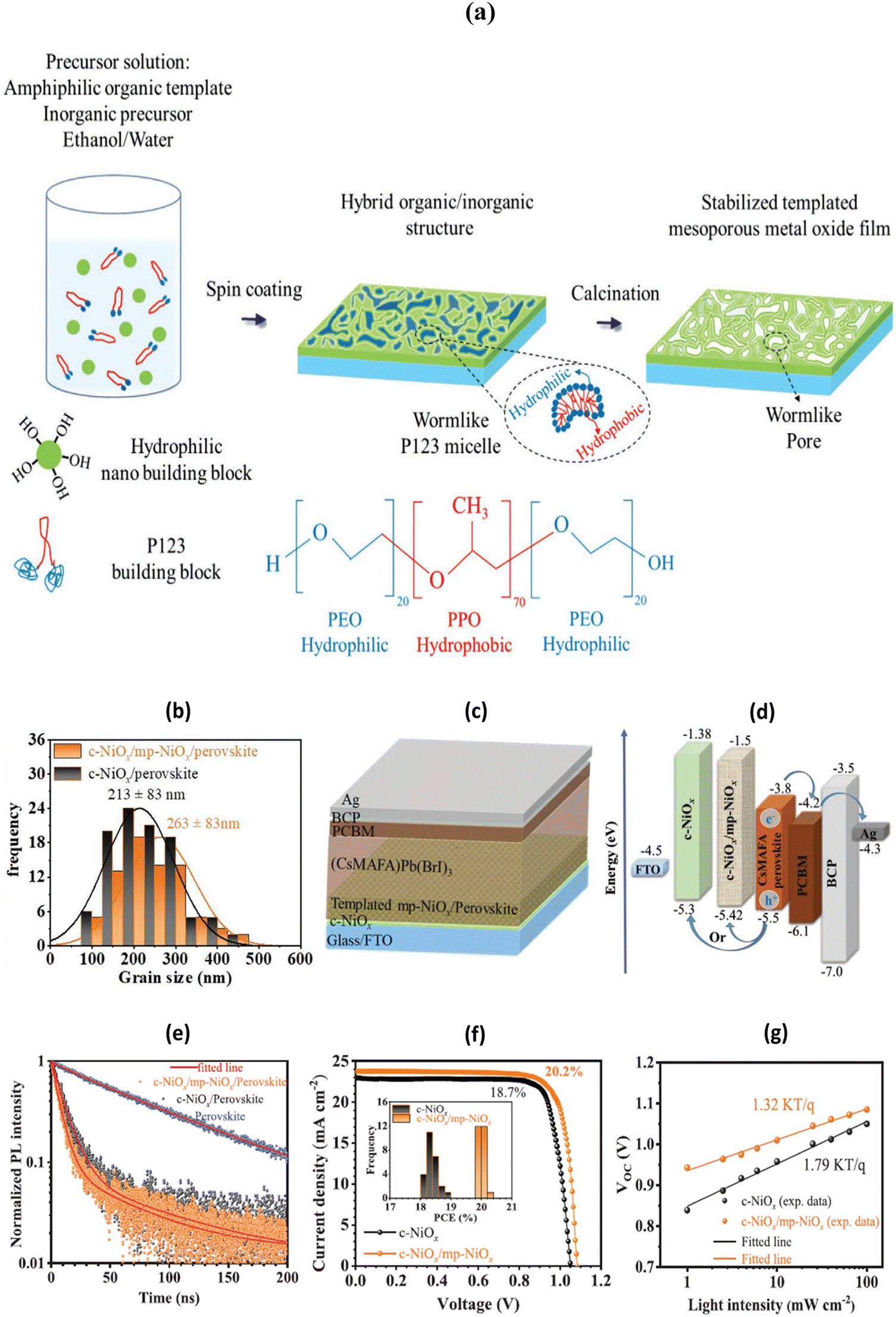 | ||
| Fig. 9 (a) An illustration of the steps undertaken in the fabrication process to prepare a P123 templated disordered mp NiOx film. (b) The corresponding histograms derived based on perovskite grain size obtained from SEM images. (c) Schematic illustration of the meso-structured PSCs. (d) Energy level diagram of the device architecture. (e) Time-resolved PL of perovskite films deposited on bare and NiOx-coated FTO substrates. (f) J–V characteristics of the best-performing PSCs based on different HTLs. The inset shows the statistics of PCE over 25 cells in each case. (g) The light intensity dependence of the VOC for planar and meso-structured PSCs. Reprinted with permission from ref. 225. Copyright 2021 John Wiley and Sons. | ||
Alternatively, NiO microspheres were employed as HTL in mp-PSCs resulting in a high PCE of 18.17% with negligible cell hysteresis.226 The optimized mp-NiO layer showed improved hole mobility and transport capability, favorable energy level alignment with the perovskite absorber, while also affected the morphology of the perovskite layer forming larger crystal grains. Interestingly, an innovative non-continuous MAPbI3−xClx–NiO NPs composite film forming an island-structure combined with the incorporation of a uniform Al2O3/NiO film between mp-TiO2 and the composite layer effectively alleviated interface recombination losses, enhanced charge transport and light harvesting, showing hysteresis-free performance with remarkable air stability.227 A schematic illustration for the preparation of the NiO microspheres and associated film/device characterization as well as the innovative non-continuous MAPbI3−xClx-NiO NPs composite film interfacial alignment are shown in Fig. 10.
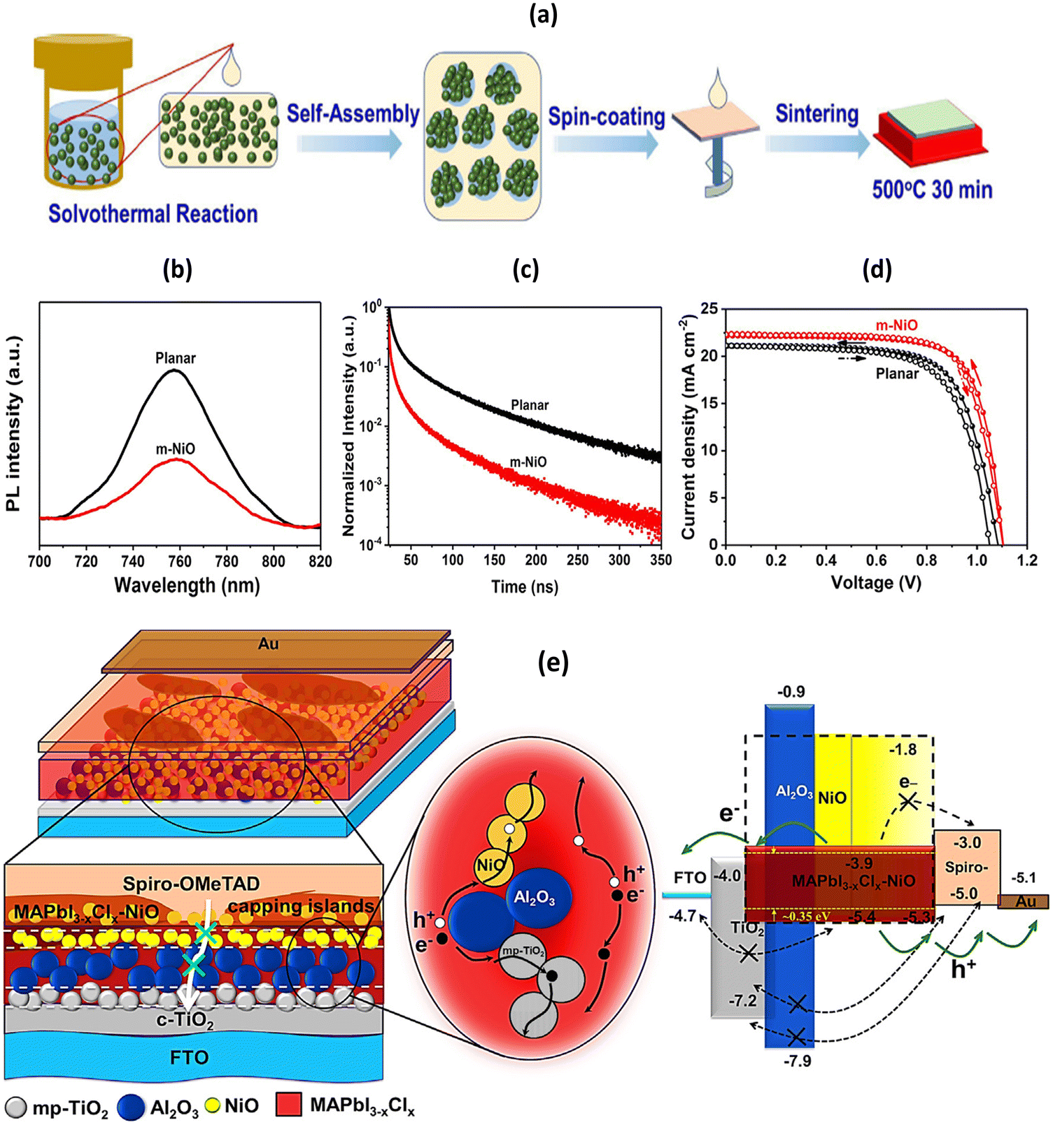 | ||
| Fig. 10 (a) Illustration of the emulsion-based bottom-up self-assembly strategy for preparing NiO microspheres. (b) PL and (c) TRPL spectra of the perovskite/m-NiO HTL/p-NiO HTL and perovskite/p-NiO HTL films. (d) J–V curves of the optimized inverted mp-PSC with m-NiO HTL and the inverted planar one with p-NiO HTL measured by forward and reverse scans. (e) Schematics of the device components and charge blocking properties upon employing islands-structure-MAPbI3−xClx–NiO layer, MAPbI3−xClx–metal oxides layers, and electron and hole transport paths and the corresponding energy level diagram. Reprinted with permission from ref. 226 and 227, respectively. Copyright 2019 Elsevier and 2018 Elsevier, respectively. | ||
Modification of NiO upon mixing with graphene was also found to facilitate charge transfer in mp-PSCs as an appropriate pore size combined with an enhanced hydrophobicity led to an improved PCE and reduced degradation in moist air.228 Novel, high quality, Ni-based mp-NiCo2O4 ternary oxide films having a regulated morphology from NSs to NWs upon increasing the hydrothermal reaction time and with a more effective hole extraction in the one dimensional NW structure were recently incorporated in PSCs with a PCE of 11.58% and a desirable long term stability.142
A different strategy for enhanced performance of mp-NiOx films was the incorporation of plasmonic nanostructures into mp films such as in mp-TiO2. For example, Au NPs were embedded into a mp-NiOx film.229 Detailed characterization revealed a novel plasmon-assisted metal-to-semiconductor charge transfer (PACT) mechanism taking place under illumination which facilitated hole extraction upon downshifting the VB edge (i.e. lowering the effective barrier height) and favored trap filling in the mp-NiOx film (see Fig. 11).
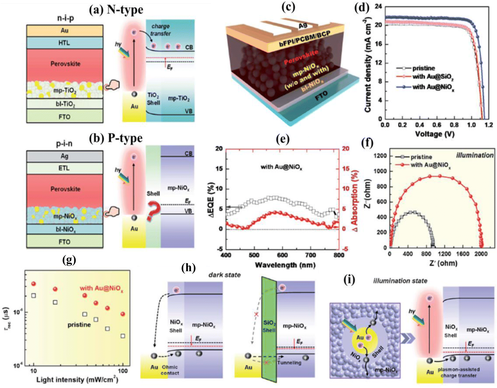 | ||
| Fig. 11 (a) Schematic illustration of Au@TiO2 shell embedment in regular mp PSCs with a TiO2 mp layer. (b) Unknown mechanism of enhancing the electronic properties of the NiOx mp layer by embedding core–shell Au NPs in inverted mp PSCs. (c) Device structure of Au NPs modified NiOx inverted mp PSCs employing a (Cs0.17FA0.83)Pb(I0.8Br0.2)3 perovskite layer. (d) J–V curves of the surface optimized PSCs prepared without and with modification of the NiOx HTL. (e) Comparison of the enhanced EQE ratio with absorption changes caused by incorporating a Au NP modified NiOx mp HTL. (f) Nyquist plots, obtained by employing electrochemical impedance spectroscopy, under illumination conditions at a bias of 1.0 V for CsFA-based PSCs with and without Au@NiOx incorporation. (g) Charge recombination lifetime extracted from transient photovoltage spectra as a function of illumination intensity for PSCs based on pristine and Au@NiOx-modified mp NiOx. Schematics of energy level alignment upon forming an ohmic contact with modified NiOx films in the dark (h) and via a novel plasmon-assisted metal-to-semiconductor charge transfer mechanism upon illumination (i). Reprinted with permission from ref. 229. Copyright 2021 Royal Society of Chemistry. | ||
As a result, inverted mp-PSCs with a very high PCE of 20.6% were demonstrated, paving the way for the use of more advanced metal or semiconductor plasmonic structures or metal oxide nanostructures to further increase the PCE of mp-PSCs. For example, a periodic array of hexagonal NiOx nanoprisms increased the efficiency of mp inverted n–i–p PSCs by 42% as it facilitated carrier transport.230 Note that, similar to the role of a compact TiO2 film, a compact NiOx film is generally highly effective in electron blocking and avoiding undesirable interfacial recombination in mp-NiOx based PSCs with ITO or FTO electrodes. Moreover, recent work has highlighted the working mechanism of alternatively incorporating a thin insulating mp scaffold Al2O3 interlayer at the bottom electrode in both p–i–n and n–i–p mp structures unveiling the dependency of the perovskite electronic structure on its physical confinement with the mp scaffold and the overall improved interfacial band alignment.231
In the quest for other novel mp inorganic metal-oxide based HTLs, a recent breakthrough was the incorporation of a mp ternary metal oxide, namely CuGaO2, with a graded band alignment in combination with a compact NiOx film to form a bilayer structure. Interfacial energy level grading led to a more effective hole transfer and reduced carrier recombination whereas the mp structure facilitated hole extraction due to the increased interfacial contact area with the perovskite film. Stabilized PCEs of ≈20% were achieved in inverted PSCs which retained more than 80% of their initial efficiency upon thermal aging at 85 °C for 1000 h, thus demonstrating superior thermal stability.145 Other doped p-type inorganic semiconducting ternary metal oxides, such as e.g. Mg2+ doped ternary CuCrO2 (M:CCO) NCs synthesized using a hydrothermal method, were also incorporated as mp-HTLs in PSCs. In that case, Mg ion doping resulted in increased hole conductivity and its mp structure atop an 5 nm compact NiOx film to create a bilayer HTL with graded energy levels reduced the interfacial offset for hole transfer, accelerated hole transport and collection, improved light-harvesting (due to reduced light reflection and enhanced light trapping in M:CCO) and suppressed carrier recombination, thus resulting in an exceptional PCE of 21.64% for inverted MA-free, cesium/formamidinium-based PSCs with excellent long-term stability: only a 19% and 20% reduction of the initial PCEs upon 1 sun light soaking for 400 h and thermal stress at 85 °C for 1000 h, respectively.148 Remarkably, an invasive plant (Eichhornia crassipes) extracted porous graphitic carbon (EC-GC) with an annealing temperature-dependent degree of graphitization was recently demonstrated to act as an exceptional HTL (as well as a counter electrode) in regular MAPbI3−xClx based mp-PSCs, exhibiting a PCE of 8.52% and impressive air stability retaining ∼94.40% of its initial efficiency for 1000 h by acting as a self-encapsulating hydrophobic layer, paving the way for the application of novel porous carbon-based materials as mp layers also in inverted n–i–p PSCs.232
In Table 2, a summary on the best performance attained for n–i–p and p–i–n mp-PSCs based on selected planar and mp HTMs is given.
| Planar or mp HTL | mp-PSC structure | PCE (%) | Ref. |
|---|---|---|---|
| Ammonium iodide doped Spiro-OMeTAD | FTO/TiO2/CsMAFAPbI3/ammonium iodide doped Spiro-OMeTAD/Au | 21.90 | 143 |
| TbT-3 (thiophene-based HTM) | FTO/TiO2/(FAPbI3)0.85(MAPbBr3)0.15/TbT-3/Au | 18.40 | 159 |
| Corrole based HTM | FTO/TiO2/MAPbI3/Corrole based HTM/Au | 19.20 | 166 |
| Quinacridone (QA) based dye | FTO/TiO2/MAPbI3/QA/Au | 18.20 | 169 |
| Porphyrin | FTO/TiO2/MAPbI3/Porphyrin/Au | 19.44 | 175 |
| Li-TFSI and TBP doped P3HT | FTO/TiO2/CsFAMAPbIxBr3−x/Li-TFSI and TBP doped P3HT/Ag | 19.25 | 186 |
| P3HT | FTO/mp-TiO2/narrow-band gap halide perovskite/thin wide band gap halide perovskite/P3HT/Au | 22.70 | 188 |
| Li-TFSI and TBP doped PTAA | FTO/TiO2/FAPbI3/Li-TFSI and TBP doped PTAA/Ag | 20.10 | 190 |
| PEDOT:PSS | FTO/TiO2/(FAPbI3)0.85(MAPbBr3)0.15/PEDOT:PSS derivatives/Au | 16.20 | 198 |
| PDTIDTBT | FTO/TiO2/CsFAMAPbIxBr3−x/PDTIDTBT/Au | 19.89 | 203 |
| mp NiOx film | ITO/NiOx/Cs0.05(MA0.15FA0.85)0.95Pb(Br0.15I0.85)3/PCBM/BCP/Ag | 20.20 | 225 |
| mp NiO microspheres | FTO/NiO microspheres/MAPbI3/PCBM/BCP/Au | 18.17 | 226 |
| mp NiOx:Au NPs | ITO/NiOx:Au NPs/CsFAPbIxBr3−x/PCBM/BCP/Ag | 20.60 | 229 |
| mp CuGaO2 | ITO/NiO/CuGaO2/CsFAPbIxBr3−x/PCBM/BCP/Au | 20.00 | 145 |
| mp Mg doped CuCrO2 NCs | ITO/NiO/Mg doped CuCrO2 NCs/Cs0.15FA0.85Pb(I0.9Br0.1)3/PCBM/BCP/Al | 21.64 | 148 |
5. HTM-free, fully printable, triple mp-PSCs
Although a huge amount of work has been made on the field of interfacial engineering in mp-PSCs demonstrating high efficiencies and long-term stabilities, printable devices are necessary for the commercialization of mp-PSCs. To this end, one of the most promising structures demonstrating high PCEs, unprecedented stabilities and recycling capability is the printable hole-conductor-free (HTM-free) triple mp-PSC using monolithic mesoporous electrodes sequentially deposited on a TCO substrate.Typically, a HTM-free triple mp-PSC consists of a thick mp ETL (e.g. TiO2 or SnO2 with a typical thickness of ∼1 μm), a few μm (∼1–5 μm) thick mp insulator (e.g. ZrO2 or Al2O3) and a thick mp carbon-based capping layer (typical thickness ∼5–10 μm) as the counter electrode (CE) sequentially deposited in a triple mesoscopic configuration (Fig. 2).233 The perovskite is the final layer deposited afterwards from solution, typically by drop casting, infiltrating through the three mp layers. The mp insulating layer is used to physically separate the bottom ETL from the top CE, preventing the formation of a mp ETL/carbon CE interface which would facilitate charge recombination as no HTM is present to avoid direct contact between the ETL and the CE. This architecture poses the advantages of having an increased number of nucleation sites for perovskite film formation and a very large mp scaffold/perovskite interfacial area for fast carrier transport with the additional benefit of the triple mp scaffold deposited by screen printing. Key factors for high device performance is the morphology of the mp ETL and the porosity of the insulating layer as both will determine the effectiveness of the perovskite infiltration and the mp-ETL pore filling. Thermal stability of the mp ETL is also of high importance as multiple annealing steps at high temperatures may be required to create the triple mp scaffold. However, as the ETL layer is thicker than that in conventional PSCs, an increased interfacial contact area exists between perovskite and ETL, leading to more significant resistive and interfacial recombination losses due to the presence of a large density of trap states on the surface of the ETL. Bulk recombination is also a serious concern inside the perovskite layer filling the insulating layer which is necessary to prevent direct contact between the anode and the cathode electrode. Note that as the triple mp scaffold is micrometer-thick, it determines the charge diffusion length in the device, whereas device performance may also be limited by poor charge transport and collection at the various interfaces as a result of the band offsets present, thus requiring to adjust interfacial energy level alignment to favor charge transfer/extraction. Concerning the earth abundant and low cost carbon-based CE which are certainly prerequisites for large scale manufacturing of PSCs, its thickness (optimum values between 5 and 10 μm) is critical in order to balance a sufficient electrode electrical conductivity with an efficient perovskite infiltration (i.e. an increased thickness results in larger conductivity but makes perovskite infiltration through the mp layers increasingly difficult). Moreover, its highly controllable and easily tunable, relatively high, workfunction (∼5.0 eV) ensures efficient hole collection while its highly hydrophobic nature represents a clear benefit for blocking moisture penentration and enhancing device ambient stability. Furthermore, its high thermal conductivity, excellent mechanical strength and large chemical stability makes it an ideal candidate for a CE material compared to metallic or semiconducting electrodes that are prone to degradation either by oxidation or by reaction with the decomposition products of perovskite under continuous cell operation. Note that among carbon-based allotropes that can be employed as CEs, carbon black and graphite are generally low cost and earth abundant materials whereas another advantage is the capability to create different carbon-based nanostructures such as zero-dimensional carbon dots, one-dimensional carbon nanotubes and two-dimensional graphene with tunable optoelectronic properties.
5.1 mp-ETLs employed in HTM-free mp-PSCs
Han's group first demonstrated a fully-printable (FP) HTM-free mp-PSC using a triple-layer device architecture including a carbon CE.234 Three mp layers consisting of TiO2, a ZrO2 spacer layer, and a carbon electrode, were deposited on an FTO substrate, while MAPbI3 infiltrated the triple-layer forming an effective TiO2/perovskite heterojunction. The fabricated cells exhibited good performance due to the capability of MAPbI3 to act as light-harvesting material and hole-conductor, as well, where the photogenerated holes were efficiently collected directly by the carbon electrode. One of the advantages of the proposed architecture is the abjuring of the expensive HTMs (such as Spiro-OMeTAD and PTAA) as already mentioned. More interestingly, the mp-PSCs based on the HTM-free structure are a promising class of devices for commercialization, since they can be fabricated by screen and ink-jet printing methods which are compatible for R2R production. The first reported fully-printable mp-PSC exhibited a PCE of 6.64%, while a year after they demonstrated improved device performance of 7.02% using a highly ordered mp carbon as counter electrode in MAPbI3/TiO2 HTM-free mp-PSC.235 The uniform mesopores along with the interconnected structures in the carbon CE led to the reduction of the charge transfer resistance at the perovskite/carbon interface, as revealed from electrochemical impedance spectroscopic measurements, and thus increase in FF and PCE values. Rong et al. also investigated the role of TiO2 nanostructure on the HTM-free mp-PSC performance.236 Interestingly, the use of TiO2 NSs with high levels of exposed (001) facets improved the interfacial properties between the perovskite absorber and the electron collection layer, compared with the TiO2 NPs, reporting an enhancement of device efficiency of 10.64%. In another study, Hu et al. successfully introduced formamidinium lead trihalide (FAPbI3) perovskite as light-harvester in HTM-free FP-mp-PSCs based on a carbon CE.237 A PCE of 11.9% was achieved for the FAPbI3-based cell, while high efficiency of 12.9% was reported for the mp-PSC using a mixed perovskite layer consisting of formamidinium and methylammonium cations of 3![[thin space (1/6-em)]](https://www.rsc.org/images/entities/char_2009.gif) :2 molar ratio. Mei et al. developed a mixed perovskite absorber by introducing 5-ammoniumvalerc acid (5-AVA) into the methylammonium iodide (MA) and lead iodide (PbI2) solution.238Fig. 12a–c shows the schematic illustration of the triple-layer perovskite junction with the corresponding energy level of the fabricated devices.
:2 molar ratio. Mei et al. developed a mixed perovskite absorber by introducing 5-ammoniumvalerc acid (5-AVA) into the methylammonium iodide (MA) and lead iodide (PbI2) solution.238Fig. 12a–c shows the schematic illustration of the triple-layer perovskite junction with the corresponding energy level of the fabricated devices.
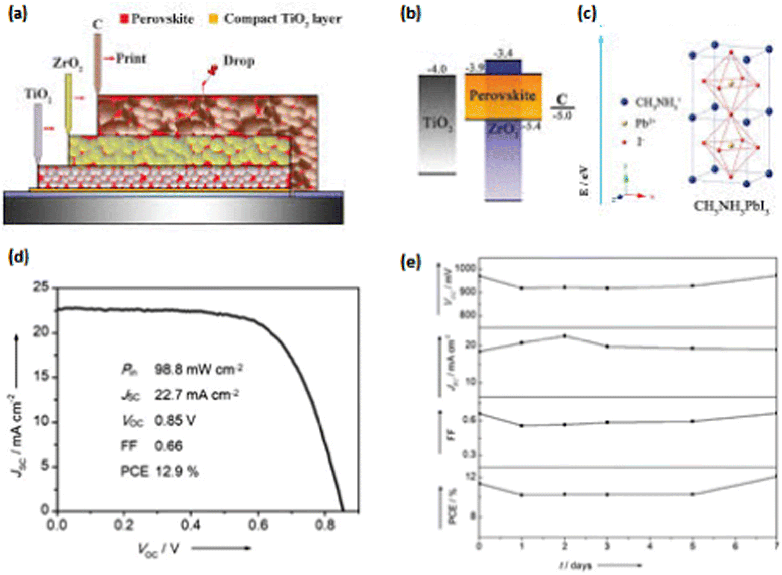 | ||
| Fig. 12 Schematic drawing showing the cross section of the triple-layer perovskite-based fully printable mesoscopic solar cell. The mp layers of TiO2 and ZrO2 have a thickness of ∼1 and 2 mm, respectively, and are deposited on a FTO-covered glass sheet shown in blue and gray. They are infiltrated with perovskite by drop-casting from solution. (b) Energy band diagram of the triple-layer device. Energies are expressed in electron volts, using the electron energy in vacuum as a reference. The energy levels of the conduction band edges of TiO2, ZrO2, and MAPbI3 are at −4.0, −3.4, and −3.9 eV, respectively, whereas the VB edge of the perovskite is at −5.4 eV and that of the Fermi level of carbon is at −5.0 eV. (c) The crystal structure of MAPbI3 perovskite. (d) J–V curves for the best performing device under simulated standard AM1.5 solar irradiation measured at room temperature. (e) Time evolution of the encapsulated PSC solar cell metrics during outdoor aging in Jeddah, Saudi Arabia. Reprinted with permission from ref. 238 and 240, respectively. Copyright 2014 AAAS and 2015 John Wiley and Sons, respectively. | ||
The corresponding mixed perovskite, (5-AVA)x(MA)1−xPbI3, employed in hole-conductor-free, FP-mp-PSC using a double layer of mp-TiO2 and m-ZrO2 as a scaffold, reporting a certified PCE of 12.84%. More importantly, the fabricated cells showed good stability for over 1000 h in ambient conditions under sunlight, attributed to the poor defects and better pore filling of the mixed perovskite crystals, leading to favorable physical contact with the mp-TiO2 and hence improved exciton lifetime. However, the devices suffered from recombination losses and thus low VOC. Recently, Seng et al. demonstrated reduced charge recombination leading to improved VOC, by using the mixed (5-AVA)xMA1−xPbI3−y(BF4)y perovskite in hole-conductor-free printable mp-PSC based on mp-TiO2/ZrO2 scaffold layer.239 The optimized (5-AVA)0.034MA0.966PbI2.95(BF4)0.05-cell exhibited a high PCE of 15.5% with improved VOC value of 0.97 V, ascribed to the formation of high-quality perovskite crystals. After the successful use of mixed (5-AVA)x(MA)1−xPbI3 perovskite, the outdoor stability of the HTM-free mp-PSCs based on mp-TiO2 and ZrO2 scaffolds and carbon CE were investigated.240 The outdoor stability tests showed negligible device degradation under 3 months heat exposure at 80–85 °C, paving the way to commercialization of mp-PSCs. Fig. 12d shows the J–V curves of the optimum HTM-free mp-PSC under AM1.5 solar illumination, while the results of outdoor stability tests are also presented (Fig. 12e).
Importantly, ZrO2 layer thickness on a double mp TiO2/ZrO2 scaffold layer needs to be optimized to obtain high device performance as it has been demonstrated to have a strong impact on the TiO2 film surface roughness and the formation of a compact homogeneous perovskite film and a defect-free perovskite/CE interface, on charge recombination rate by preventing back electron transport from TiO2 to CE and, obviously, on charge transport resistance. A film thickness of 167 nm was, for example, found optimal for mixed-cation based m-PSCs with a PCE of 11.33%.241 Moreover, double-layered ZrO2 consisting of ZrO2 NPs and microparticles exploited the ability of the microparticles to scatter and hence diffuse the incident light, thus enhancing light-harvesting in the perovskite with a concomitant increase of the device photocurrent and the PCE.242
As the key component of hole-conductor-free printable mp-PSCs, the morphological characteristics of mp-TiO2 play critical role in device fabrication and performance. Yang et al. investigated the influence of the size of TiO2 NPs used a scaffold in combination with the ZrO2 layer on the efficiency of printable mp-PSCs.243 It was demonstrated that the infiltration of the mixed (5-AVA)x(MA)1−xPbI3 perovskite absorber, used in this study, was affected by the size of TiO2 NPs, along with the charge transfer at the perovskite/TiO2 interface. The optimized cell based on the TiO2 NPs with diameter of 25 nm and the carbon CE, exhibited high PCE value of 13.41% as it allowed effective perovskite infiltration in the relatively large pores. Interestingly, nanoporous submicron TiO2 spheres with diameters around 200 nm as a high surface area scaffold layer improved perovskite infiltration, light-harvesting due to enhanced scattering and electron transport resulting in an increased PCE of 14.3% and excellent stability against moisture under ambient conditions.244 Alternatively, a dual-sized TiO2 scaffold layer prepared upon dispersing 100 nm-sized TiO2 NPs into a conventional TiO2 scaffold layer composed of 25 nm-sized TiO2 NPs exhibited not only a superior light-harvesting ability of the 100 nm TiO2 NPs due to increased light scattering but also complete perovskite infiltration into the scaffold due to the larger voids formed, leading to a ∼19% higher PCE compared to the conventional scaffold.245
Another simple and effective strategy used to reduce charge recombination between mp-TiO2 and carbon CE is the modification of mp-TiO2 with appropriate materials. As already mentioned in the case of ETL modification in mp-PCs, a thin modifying layer could effectively tune the morphological and optoelectronic properties of the ETLs facilitating charge transport and hence improving device performance. For example, Wang et al. sprayed an ultrathin (2.4 nm) Al2O3 onto mp-TiO2 deposited via screen-printing on c-TiO2 layer.246 The introduction of this ultrathin insulator in the FP-mp-PSC modified the conduction band minimum of mp-TiO2 to a lower energy, as well as, reduced the density of dangling bonds on the mp-TiO2 surface, which were beneficial to electron transfer from the perovskite absorber to the mp-TiO2 layer. The successful Al2O3 modification of TiO2 in respect with the optimization of mp-ZrO2 thickness, resulted in enhancement of the mp-PSC performance. Moreover, taking advantage of high electron mobility of C60, Han's group proposed the deposition of a thin C60 layer on TiO2 using a spray method to prevent charge accumulation and recombination resulting in improved efficiency of the HTM-free FP-mp-PSC based on carbon CE.247 C60-modified TiO2 exhibited a more favorable energy level alignment at the ETL/perovskite interface than that of the pristine TiO2, ascribed to the up-shifted LUMO of the TiO2(C60) leading to increased VOC. Consequently, a high PCE of 15.38% was achieved for the mp-PSC with the TiO2(C60)/ZrO2/carbon structure showing reduced hysteresis compared with the reference cell using the pristine TiO2 layer. In another recent approach, Xu et al. used dually the commercial dye N719, as a surface modifier of TiO2 and a suppressor of defects appeared on the surface of the perovskite layer.248 In particular, TiO2 NPs sensitized by a N719 ethanol solution were added in the perovskite solution to promote the passivation of MA defects on the surface of the perovskite layer. Interestingly, the TiO2 NPs acted as core facilitating crystallization, while the unbounded carboxyl groups on the surface of the N719-modified TiO2 acted as a shell, interacting with the MA and hence improving the suppressing effect. Shallow defects acting as trap-states of the photogenerated charges were reduced boosting the enhancement of charge extraction efficiency, as well as, the performance of mp-PSCs. Recently, an interesting alternative strategy was proposed by Tao et al. who incorporated a luminescent down-conversion material, namely a europium polyoxometalate compound (EuW10) into mp TiO2 resulting in an enhanced JSC and FF and an increased PCE from 11.42% to of 14.36%.249
To further improve the interfacial contact between the mp-TiO2 and the perovskite light-harvester, surface modification of TiO2 using a silane self-assembled monolayer (SAM) was proposed by Liu et al.250 The introduction of silane SAM tuned the electronic structure at the TiO2/perovskite interface leading to favorable energy level alignment, while also acted as a passivation layer reducing the charge recombination losses. Consequently, efficient hole-conductor-free mp-PSCs were fabricated with high PCE of 12.7%. Xiao et al. employed W-doped TiO2 as ETL in mp-PSC reporting an 15.7% enhancement of cell performance compared to that with the undoped TiO2.251 This significant improvement of device efficiency attributed to the improved conductivity of W-doped TiO2, as well as, the favorable shifting in conduction band energy level, facilitating electron transport and extraction.
As previously reported, in the most representative mp-PSCs and HTM-free, fully printable mp-PSCs, a mp ETL is developed on a compact thin layer that acts as hole blocking layer to suppess shunting paths (e.g. short-circuit and leakage current) at the cathode/perovskite interface, with the most commonly used compact layer to be c-TiO2. Although the effective use of compact layer in device efficiency and stability, Jiang et al. suggested a compact-free mp-PSC in order to reduce the fabrication steps and thus the preparation cost of the cell.252 The HTM-free printable mp-PSC without compact layer using a screen-printing method demonstrated a PCE of 12.94%, comparable with that based on compact layer, verifying the efficient and simpler fabrication process of the proposed structure. Zhao et al. demonstrated the necessity of well-matched energy levels alignment at the ETL/perovskite layer to eliminate charge recombination, as well as, enhance photovoltage. The introduction of a gradient mixed zinc-tin-oxide (ZTO) bilayer, with a tunable workfunction by Zn concentration and prepared by a spray-pyrolysis process, as ETL in printable mp-PSC improved the VOC leading to high PCE of 15.86%.253 More importantly, ZTO layers facilitated electron transfer from the perovskite towards the selective electrode through the favorable cascade energy levels quenching trap-assisted charge recombination. Recently, c-TiO2 post-treated with TiCl4 and applied in HTM-free mp-PSC exhibiting improved charge transport within the cell and high performance with PCE value of 14.83% due to the limitation of charge recombination between FTO and perovskite.254 Another, simple and effective, post-treatment of the triple-mesoscopic TiO2/ZrO2/carbon scaffold with 2-phenyl-5-benzimidazole sulfonate-Na (PBS-X) resulted in an upshift of the TiO2 conduction band upon its coordination to the TiO2 NPS, favoring electron transfer and suppressing interfacial recombination, and an improved PCE of 16.51% combined with a remarkable long-term stability after 1000 h continuous illumination/operation.255 Apart from mp-TiO2, other oxides including ternary oxides in NP form have been employed but with limited success so far as mp-ETL in HTM-free carbon-based mp-PSCs. As an example, barium stannate BaSnO3 (BSO) NPs with controlled crystallinity, stoichiometry and oxygen vacancy concentration as a function of heat treatment under nitrogen or oxygen (and a combination of both) delivered a high PCE of 14.77%.256
5.2 Alternative to ZrO2 spacer layers
Besides the mp ETL, the spacer layer is a key multifunctional component that may play different roles in the efficiency of mp-PSCs. An ideal spacer layer for highly-efficient carbon-based mp-PSCs should meet the following requirements:(1) A uniform high quality film without pinholes featuring a wide bandgap to avoid electron transport from the TiO2 layer towards the carbon CE. Therefore, the particle size and morphology of the spacer materials affect the proper separation of the anode and cathode within the cell. Pore size larger than 100 nm combined with high porosity is considered ideal for a highly effective spacer layer.257 Its thickness should also be optimized in order to allow efficient charge transport and perovskite infiltration and, simultaneously, effectively separate the mp ETL from the CE. Although increased thickness insulating layers are generally more difficult to be effectively infiltrated by the perovskite solution, they can lead to optimal performance if effective ifiltration can be obtained despite the fact that holes need to travel larger distances than the typical perovskite diffusion length in that case.
(2) Excellent insulating ability to increase charge transport length through the spacer material. In particular, the photogenerated holes in the perovskite/TiO2 interface should effectively transport from the perovskite/spacer material towards the carbon CE.
(3) High CB energy level to facilitate the electron transport from the perovskite/spacer layer to the TiO2/electrode.
Note that these requirements should be met in combination with a highly spacer-infiltrated perovskite film featuring porous single crystals with few grain boundaries, preferred orientation and long carrier lifetime.
Except ZrO2, aluminum oxide (Al2O3) has also been used as spacer layer in mp-PSCs. Cao et al. fabricated efficient mp-PSCs based on the structure TiO2/Al2O3/carbon exhibiting a PCE of 11.03% when introduced MAPbI2Br perovskite as light-harvester.258 The device showed also improved charge carrier lifetime, leading to enhanced VOC value, along with good stability. Han et al. incorporated an optimum 10 nm Al2O3 layer in combination with screen-printed ZrO2 in a novel architecture design to improve the performance of AVA-MAPbI3 cells from 12% to 14% due to the increased VOC from 0.836 to 0.942 V upon reducing carrier recombination at both perovskite/ETL and perovskite/CE interfaces.259 Moreover, Meng et al. studied the influence of the spacer material pore size on the mp-PSCs performance.260 It was observed that ZrO2 formed larger pores than Al2O3 boosting the infiltration of the perovskite and improving the crystal growth of the latter in the pores, as well. In a similar context, Wang's group reported that the double mp-ETLs in HTM-free mp-PSCs was more efficient than the single mp-ETL with an enhanced PCE of 11.3% for the cell with the mp-TiO2 + Al2O3 layer due to the improved film formation leading to improved perovskite crystallization.261 Although the beneficial characteristics of spacer layers on effectively separating the TiO2 and the carbon CE, the optimization of thickness, pore size, and insulating property of the different spacer layers are crucial on the performance of HTM-free mp-PSCs. Zhang et al. used the same device structure with the Al2O3 spacer layer, although, employed an environmentally friendly strontium chloride (SrCl2) in the MAPbI3 solution forming the MAPbI3(SrCl2)x perovskite, and compared it with MAPbI3.262 The optimized MAPbI3(SrCl2)0.1 based HTM-free mp-PSC showed higher efficiency of 15.9% than that using MAPbI3, ascribed to the improved morphological properties of SrCl2-based perovskite layer with low defects and enhanced pore filling. Combining Al2O3 and ZrO2 NPs to prepare a high quality, flat, layer with enhanced insulating and better separating (TiO2 from Carbon) ability, compared to a regular spacer, led to an improved PCE of 13.8% due to suppressed charge recombination and more efficient hole collection at the defect-free perovskite/carbon interface.263
Another insulator employed in HTM-free Mp-PSCs as a spacer layer is silicon dioxide (SiO2) with large band gap and high optical transmittance in the visible range. Mp-SiO2 (mp-SiO2) with different thickness deposited on mp-TiO2 was introduced as insulating layer in MAPbI3-based mp-PSCs.264 Reduced charge recombination losses between the mp-TiO2 ETL and the carbon CE were observed when SiO2 inserted as a spacer layer resulting in enhanced VOC and FF, and hence PCE. A high PCE of 12% was achieved for the optimized device, along with improved stability reporting stable PCE after 30 days. Moreover, the effect of concentration of SiO2 paste on the formation of m-SiO2 layer was studied by Liu et al.265 For moderate concentration, uniform SiO2 without crack appearance was obtained leading to high PCE of 13.09%. More importantly, unencapsulated mp-SiO2-based mp-PSCs showed excellent long-term stability under ambient conditions with humidity of 50–70%, retaining ∼95% of its initial PCE value after 104 days.
Recently, the replacement of the spacer layer with a 40 nm thin and dense Al2O3 in a double-layered HTM-free mp-PSC based on carbon-graphite CE was proposed by Mathiazhagan et al.266 Al2O3 prevented ohmic shunts forming a pseudo-porous layer on top of mp-TiO2, which also permitted the photogenerated holes to diffuse through the perovskite crystalline regions. The fabricated HTM-free mp-PSC exhibited comparable PCE value (12.1%) with the triple-layered mp-PSC based on the same CE. Although the beneficial characteristics of the proposed double-layered mp-PSC, further investigation on whether a thinner insulator can compete the commonly used micrometer thick spacer layer or not, is needed. Interestingly, replacement of ZrO2 by mp-NiO led to an instant, facile, perovskite film formation inside the TiO2/NiO/carbon layer pores and a accelerated hole extraction with a promising PCE of 11.4%.267
5.3 Carbon and alternative, novel, materials as CEs
Carbon CE consisting mainly of graphite and carbon black or other carbon allotropes play also a very crucial role in HTM-free mp-PSCs performance to efficiently collect the photogenerated holes from the perovskite absorber due to their high conductivity and mobility and their large workfunction, thus minimizing series resistance and facilitating hole extraction. Note that a thicker, improved conductivity, CE usually results in sub-optimal perovskite infiltration which requires a necessary compromise between those two parameters for optimum device performance. Furthermore, CE porosity and conductivity are affected by the ratio between graphite and carbon black with carbon black increasing film porosity but, simultaneously, reducing its conductivity as is more resistive than graphite. As already mentioned, the first report of TiO2/ZrO2/carbon HTM-free mp-PSC architecture, in which spheroid graphite with high conductivity and good pore-filling film morphology was employed as a replacement of flaky graphite in the carbon composite layer, exhibited improved PCE (6.64% for the spheroid graphite-based device, in contrast to the 4.08% for the device using the flaky graphite). Zhang et al. studied the influence of flaky graphite's size on the graphite/carbon CE.268 Therefore, carbon CEs based on flaky graphite with different sizes were employed in HTM-free mp-PSCs with mp-TiO2/ZrO2 scaffold. An optimum 8 μm graphite based carbon CE exhibited large pore size and low square resistance resulting in high PCE of 11%. The effect of thickness of mp-carbon CE on the mp-PSCs performance was investigated by Li et al.269 Variation of device electrical parameters and thus various PCE values were obtained for different thickness of mp-carbon CEs, while good shelf-stability up to 112 days was observed for all the devices, demonstrating that mp-TiO2-bonding mp-carbon layer effectively prevented the penetration of oxygen and moisture that could lead to device degradation. It is also noteworthy that annealing of the carbon film electrode was also critical in obtaining excellent electrical and morphological properties. Although a low temperature is obviously preferred, temperatures between 250 and 300 °C were found to be ideal to obtain highly conductive carbon films with good adherence. However, annealing at temperatures larger than 300 °C was necessary, prior to infiltration of the perovskite precursor solution, to produce highly efficient printed HTM-free mp-PSCs with adequate crystallinity perovskite films, thus limiting compatibility with flexible substrates.270 Furthermore, carbon electrode treatment with a polysterene-containing toluene solution reduced perovskite agglomeration, increased optical transmission, improved charge transfer and reduced charge recombination, resulting in enhanced efficiency (14.03% vs. 11.31%) and light and ambient stability.271Recently, Jiang et al. proposed a novel hybrid carbon electrode based on a high-temperature mp carbon (mp-C) layer and a low-temperature highly conductive carbon (c-C) layer.272 In this configuration, mp-C exhibited a high work function (tunable upon adding different amounts of NiO) and a large surface area which facilitated charge extraction and enhanced VOC when combined with a ZrO2 layer thickness of ∼1 μm whereas c-C layer had a large conductivity which was conducive for facile charge transport. The workfunction of a carbon CE which is critical to obtain a high VOC could also be increased from 4.81 eV to 5.10 eV upon incorporating B atoms into graphite lattice leading to a high workfunction boron-doped carbon CE combined with an improved conductivity due to the higher graphitization carbon of boron-doped graphite. This led to a 10% improvement of the device PCE by increasing recombination lifetime and reducing charge transfer resistance.273 Ecofriendly, naturally extracted from aloe vera plant, cross-linked carbon NPs have also been proposed as a very low cost solution which ensures an excellent perovskite penetration in the triple mp layer scaffold and enables a high-quality perovskite crystal formation resulting in a high PCE comparable to Spiro-OMeTAD but with enlarged air and moisture stability (>1000 h at >45% relative humidity).274
In another approach, Duan et al. employed a mixed CE consisting of ultrathin graphite and carbon black paste in HTM-free FP-mp-PSC demonstrating improve hole collection, as well as, reduced charge transfer resistance between the perovskite and the carbon CE, leading to higher device efficiency of 14.07% compared with the 12.63% PCE of the cell based on bulk graphite-mixed carbon CE.275 Moreover, improved perovskite infiltration was observed due to the larger specific surface area of the ultrathin graphite based CE. Fig. 13(a–d) shows the scanning electron microscopy (SEM) images of ultrathin and bulk graphite powders. The device structure along with the cross-sectional SEM images are presented in Fig. 13(e–g), and the J–V curves of the devices are shown in Fig. 13(h).
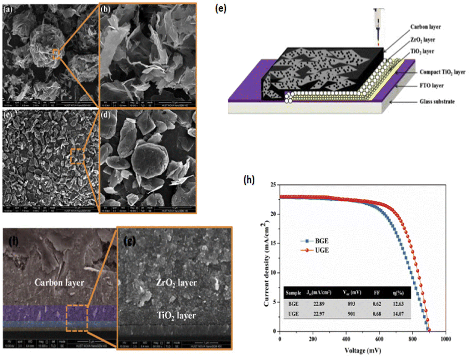 | ||
| Fig. 13 Morphology of (a and b) ultrathin graphite and (c and d) bulk graphite powders at low and high magnification. (e) Schematic structure of a hole-conductor-free mesoscopic PSC device based on carbon electrode. (f) Cross-sectional SEM image of the PSC device. (g) Enlarged image of the marked area in (f). (h) J–V curves of the PSC device based on ultrathin and bulk graphite electrode. Reprinted with permission from ref. 275. Copyright 2017 Elsevier. | ||
Improved charge transport properties within the mp-PSC attributed to the good contact at the perovskite/CE were also reported by Yue et al. and Mashreghi et al. by incorporating a low-temperature graphite/carbon black CE in the cell.276,277 Mariani et al. reported a low temperature-processed graphene-based carbon paste with improved thermal stability and exceptional performance for both small (0.09 cm2) and large-area (1 cm2) as well as miniwafer-like area (with a 4 cm2 aperture area) cells reaching PCEs of 15.81%, 13.85% and 12.10%, respectively, which are among the highest reported for large and wafer-like area cells.278 An improved performance carbon black/graphite paste could be obtained upon directly inserting in it Ni precursor solutions which resulted, upon annealing, in the formation of Ni nanostructures, a higher hole mobility and a lower trap density in the modified paste which served as a more efficient CE.279 Furthermore, hydrophobic carbon/graphite nanocomposites with impressive transport properties improved significantly their conductivity and hydrophobicity upon compression, thus enhancing photovoltaic performance and exhibiting remarkable ambient stability for more than 7000 h.280
To further improve charge extraction and collection, a multi-layered PIN architecture was employed. Wang and co-workers proposed the use of a quadrupble-layered structure consisting of mp TiO2, Al2O3, nickel oxide (NiO), and carbon, as a scaffold for the infiltration of MAPbI3.281 In contrast to previously mentioned studies, the insertion of mp NiO, as a p-type semiconductor, could be beneficial to hole extraction. The corresponding mp-PSC fabricated by FP-methods exhibited high performance of 15.03%, originated by the dual role of NiO layer, as a spacer and a HTL, as well, indicating the improved hole transport from the perovskite absorber to the carbon CE through the hole selective NiO. The good long-term stability of the device based on the quadrupble-layered architecture paves the way towards the commercialization of HTM-free Mp-PSCs. By adopting the same device architecture, Behrouznejad et al. performed a UV-ozone treatment on mp-NiO layer, resulting in increased Ni3+ phase on NiO surface and thus enhanced conductivity, as revealed from X-ray photoelectron spectroscopy.282 In addition, they investigated the effect of Al2O3 thickness on mp-PSCs. It was observed that for thin Al2O3 layer of 200 nm defects at the perovskite/Al2O3 interface were produced, while for thicker Al2O3 layer of 700 nm defects were appeared in the perovskite/Al2O3 composite layer. In both cases, low VOC was obtained. The best performance was achieved for the mp-PSC based on the optimized Al2O3 with thickness of 450 nm. A high efficiency of 17.02% was reported by Liu et al. upon introducing a triple cation perovskite absorber, in particular, Cs0.05(FA0.4MA0.6)0.95PbI2.8Br0.2 in FP-mp-PSCs with the mp TiO2/Al2O3/NiO/carbon structure.283 Not only was the effective strategy of PIN architecture demonstrated, but also the successful and efficient partial replacement of FA/MA by cesium in the perovskite absorber. Cs-based perovskite layer exhibited increased charge carrier lifetime facilitating charge transport, while the corresponding cell showed good long-term stability maintaining the 90% of its initial PCE value after 1020 h.
Enhanced CE's conductivity could readily be obtained when suitable p-type materials were incorporated in the carbon-based layer. Hu et al. synthesized copper sulfide (CuS) nanostructures, which were incorporated in the graphite/carbon CE.284 Improved hole transfer from the perovskite to the CE was obtained attributed to the high hole mobility of the CuS, leading to an increase in mp-PSC's performance with PCE of 11.28%, which was slightly higher than that without the CuS. Another p-type semiconductor was introduced into the carbon paste by Chu et al. In particular, NiO2 NPs exhibiting facile hole transport were incorporated in the carbon CE boosting the efficiency of the fabricated mp-PSCs to 13.26%, a PCE almost equal to that using the Spiro-OMeTAD HTL and Ag anode (PCE of 13.24%).285 Recently, Bhandari et al. investigated the effect of WO3 on carbon CE.286 WO3 NPs were introduced in the carbon layer and applied as CE in mp-PSCs with the TiO2/Al2O3/MAPbI3 structure reporting good long-term stability after 500 h under ambient conditions and light illumination. Similarly, Zhou et al. incorporated WO3 NPs as additives in the carbon electrode to promote hole extraction at the perovskite/carbon interface due to the favorable energy band alignment at the carbon/WO3/perovskite interface.287 Furthermore, chemical doping was proposed by Chen et al. to enhance the conductivity and tune the work function of the carbon CE in HTM-free mp-PSCs.288 Therefore, boron (B) and phosphorus (P) co-doped bilayer carbon CE applied as efficient hole extraction layer. Improved device performance was obtained due to the increase of work function of the B-doped carbon film leading to enhanced p-type conductivity, and also to decrease of sheet resistance of the P-doped carbon layer. A novel highly-conductive, low-temperature (<100 °C), carbon paste with a superior electrical characteristics was obtained by Jiang et al. upon incorporating functional additives of titanium(IV) isopropoxide and acetic acid to generate newly polymeric Ti–O–Ti complex species, acting as binder and plasticizer, which increased the film electrical conductivity (obtaining a very low sheet resistance of 4 Ω sq−1 for a 20 μm film, superior to FTO/ITO) and delivered a champion PCE of 14.04%.289 It is noteworthy that a TiO2 NP binding carbon electrode combined with vacuum treatment to facilitate perovskite infiltration and film formation led to a larger interfacial contact area, enhanced charge extraction and increased efficiency and stability.290 Interface modification for more efficient hole extraction was recently proposed with a high conductivity liquid metal (LM) in combination with a carbon electrode which decreased interfacial charge transfer resistance and led to a 26% increase of the PCE.291 In order to improve the contact between the perovskite and the carbon CE, and also the contact at the carbon black/graphite interface, Zhang et al. first introduced a facile vibration method of CE, reporting FF and JSC enhancement and a PCE of 10.37% for optimized PSCs with vibration time of 10 min, which was much higher of that based on the untreated CE (PCE of 8.5%).292 Note that this vibration method may be promising for large-scale production of HTM-free mp-PSCs.
Regarding alternatives electrode materials, Zhang et al. proposed for the first time an innovative strategy using solution-processed hydrogen molybdenum bronze (HxMoO3−y) nanobelts, an n-type HTM with very high work function and large electrical conductivity, as an alternative to carbon to enhance hole extraction ability and form a more favorable energy alignment in order to realize 14.5% efficient devices based on the FTO/c-TiO2/mp-TiO2/mp-Al2O3/HxMoO3−y triple-mesoscopic architecture (see Fig. 14a–c).293 Impressively, oxygen-rich activated carbon, synthesized from cellulose (termed CAC), exhibited a very high specific area of 477.14 m2 g−1, possessed a high oxygen content of 11.9% and had an increased workfunction (approaching the perovskite valence band energy), thus improving its wettability, the interfacial carbon electrode/perovskite contact and the efficient penetration of the perovskite through the mp scaffold and facilitating barrier-free hole extraction. As a result, (5-AVA)0.03(MA)0.97PbI3 based mp-PSCs with an efficiency of 15.5% were demonstrated, compared to 13.8% for pristine carbon electrodes (see Fig. 14d–f).294 Note that a facile oxygen management strategy in the carbon CE to tune the physical contact, as well as, the energy level alignment at the perovskite/CE interface had first been suggested by Tian et al.295 In this context, oxygen-rich carbon (ORC) black CE upon functionalization with C–OH and C![[double bond, length as m-dash]](https://www.rsc.org/images/entities/char_e001.gif) O groups exhibited enhanced p-type characteristics and a positive work function shift from 5.0 to 5.2 eV, due to oxygen's p-type doping effect. Moreover, it facilitated hole extraction from the perovskite to the CE, due to its large specific surface area promoting the improvement of contact at the perovskite/CE interface. Consequently, the fabricated HTM-free mp-PSCs based on ORC CE exhibited an excellent performance with high PCE of 15.7%. Alternatively, waste plastic derived 3D graphene NSs (GNs) including one or two graphene layers were employed as an alternative dopant in a carbon electrode to demonstrate devices with superior performance (12.40% compared to 11.04%) and a simultaneous improvement of all device parameters due to the enhanced electrode conductivity and the reduced recombination losses (see Fig. 14g–i).296
O groups exhibited enhanced p-type characteristics and a positive work function shift from 5.0 to 5.2 eV, due to oxygen's p-type doping effect. Moreover, it facilitated hole extraction from the perovskite to the CE, due to its large specific surface area promoting the improvement of contact at the perovskite/CE interface. Consequently, the fabricated HTM-free mp-PSCs based on ORC CE exhibited an excellent performance with high PCE of 15.7%. Alternatively, waste plastic derived 3D graphene NSs (GNs) including one or two graphene layers were employed as an alternative dopant in a carbon electrode to demonstrate devices with superior performance (12.40% compared to 11.04%) and a simultaneous improvement of all device parameters due to the enhanced electrode conductivity and the reduced recombination losses (see Fig. 14g–i).296
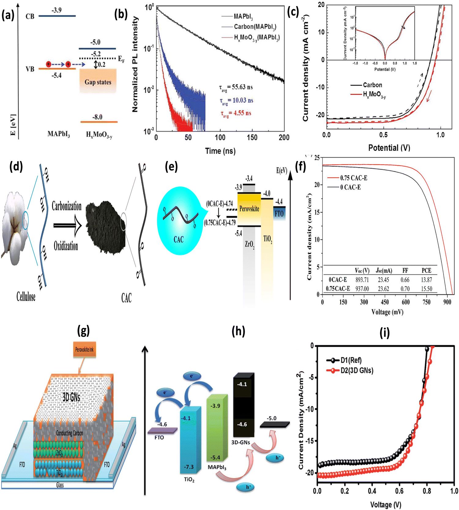 | ||
| Fig. 14 (a) Schematic energy diagram of hole transfer from perovskite to HxMoO3−y layer. (b) Time-resolved PL decay spectra of the perovskite embedded in the HxMoO3−y and high-temperature carbon films. (c) J–V curves of devices based on HxMoO3−y and carbon electrodes in the reverse and forward scan direction. Reprinted with permission from ref. 293. Copyright 2019 Royal Society of Chemistry. (d) Schematic depiction of cellulose carbonization and oxidization for obtaining cellulose-based activated oxygen-rich carbon (CAC). (e) Energy level diagram of CAC based PSCs prepared upon mixing graphite powder with 0 and 0.75 g CAC for preparing CEs (denoted as 0CAC–E and 0.75CAC–E, respectively). (f) J–V curves of 0CAC–E and 0.75CAC–E devices. Reprinted with permission from ref. 294. Copyright 2021 John Wiley and Sons. (g) Device geometry of waste plastic derived 3D graphene NSs (GN) based carbon PSCs. (h) Energy level diagram of the GN-doped PSCs. (i) J–V characteristics of devices D1 (reference) and D2 (carbon + 3D GNs). Reprinted with permission from ref. 296. Copyright 2021 Royal Society of Chemsitry. | ||
As carbon nanotubes have outstanding charge transport properties, along with excellent chemical stability and large hydrophobicity, recent work has exploited their potential as CEs in HTM-free mp-PSCs. In this framework, Mhaisalkar et al. first implemented a semitransparent carbon nanotube network coated on top of the perovskite layer acted as a hole collector, leading to improved hole extraction and a moderate PCE of 6.28%.297 Moreover, Wei et al. deposited a multi-walled carbon nanotube electrode on TiO2/perovskite substrates demonstrating highly-efficient hysteresis-free mp-PSCs with PCE of 12.67%,298 while Cheng et al. inserted multi-walled carbon nanotubes in the perovskite layer to improve charge transport and collection.299 The corresponding cells exhibited a PCE of 11.6%, which was increased by ∼15% compared with the device without the carbon nanotubes. Alternatively, 3D cross-stacked superaligned CNT sheets with excellent conductivity, porosity and flexibility were proposed instead of carbon as a CE to fabricate MAPbI3/TiO2 devices with PCE comparable to carbon which could be further enhanced upon doping the CNT sheets with iodine due to the higher CE conductivity, the improved perovskite crystallinity and its increased grain size.300 Moreover, Liu et al. demonstrated a composite NiO NP:single walled carbon nanotube (SWCNT) thin (∼1.8 μm) film as an alternative to a thick (typically ∼10 μm) carbon/graphite CE to obtain enhanced conductivity (by adding SWCNTs) and, consequently, charge collection and an increased PCE of 12.7% for MAPbI3 cells using a TiO2/Al2O3 scaffold with good ambient stability.301 To enhance CE conductivity and workfunction, doping of a graphite/carbon CE with SWCNTs was proposed and delivered a superior performance with a PCE of a 14.7% for a MAPbI3 device due to the enhanced hole collection and the increased recombination lifetime.302 Alternatively, aluminum and copper grids embedded in carbon were explored as potential mp CEs due to their large conductivity combined with their low cost and facile preparation. As a result, a lower sheet resistance CE was demonstrated which led not only to an enhanced FF and a higher PCE of 11.07% for a 11.7 cm2 active cell area but also to improved mechanical durability and increased photostability.303
Furthermore, high conductivity needle coke (NC) was used for the first time as a novel replacement of carbon black in the carbon paste for triple mp PSCs by Wu's group.304 The excellent efficiency of 11.66% for the NC-based cell was ascribed to the enhanced morphology and crystallization of the perovskite resulting in decrease of the leakage current and recombination losses combined with the enhanced charge separation and hole extraction of the enhanced conductivity NC Moreover, Wei et al. demonstrated a low-cost and environmental friendly clamping PSC of high performance and good long-term stability.305 An abundant candle soot used as an efficient hole selective electrode in the nanocarbon-based clamping PSCs exhibiting a PCE of 11.02%. This study paves the way to roll-to-roll production and thus the commercialization of PSCs. Furthermore, Meng's group employed for the first time a free-standing flexible carbon CE of good conductivity exhibiting a high PCE value of 13.53% paving the way for flexible, HTM-free, carbon CE-based mp-PSCs.306 Recently, screen printed mp ITO was proposed by Schneider et al. as an alternative CE for hole collection in triple mesoscopic HTM-free mp-PSCs with an FTO/mp TiO2/mp ZrO2/mp ITO structure, demonstrating a PCE of 9.37% and a remarkable ambient cell stability retaining 96% of their initial PCE after 1000 h.307 Moreover, recycling of the perovskite, upon rinsing it and re-depositing it from a new solution, was achieved in consecutive cycles with an excellent cell reproducibility and a slight enhancement in the overall performance. Post treatment of the mp ITO upon dipping in a MAI solution and subsequent heating led to an improved PCE due to the enhanced perovskite infiltration as demonstrated by Saleh et al.308 Similar work with MAPbI3 and a Sn-based perovskite (GAFASnI3) resulted in PCEs of 11.3% and 4.7%, respectively, with an enhanced stability compared to a carbon CE, upon optimizing the mp ITO thickness to ∼7.8 μm in order to achieve a balance between perovskite infiltration and pore filling and good electrode conductivity.309
Considering the aforementioned advances in fabrication and processing of HTM-free mp-PSCs, it is of no surprise that multiple cation (including FA, Cs and Rb) and mixed I/Br halide containing perovskites with different formulations could attain complete crystallization of the perovskite phase (without the use of an antisolvent), demonstrated low series and large recombination resistance and found to be highly efficient and very stable in ambient conditions.310
6. Conclusions and future outlook
Herein, we provided an authoritative review on the recent achievements and progress made in various charge transport materials used as well as feasible strategies pursued for interfacial engineering of mp-PSCs in both n–i–p and p–i–n architectures. In particular, interfacial materials successfully employed as electron and hole transport layers in mp-PSCs were analytically presented and discussed with regard to their functionalities and how these affect device performance (efficiency and stability). Inorganic metal oxides and organic materials with desirable optoelectronic properties and excellent intrinsic stability represent the two large families of compounds incorporated as HTLs/ETLs in mp-PSCs. N-type metal oxides such as TiO2 SnO2 and ZnO in various forms and structures have been widely employed as mp-ETLs in the mp n–i–p architecture whereas p-type oxides such as NiOx has been the main candidate for the mp p–i–n architecture. Although these materials can be deposited by solution processing, the disadvantage of high temperature sintering has turned the research community's interest more to organic materials as potential alternatives for the fabrication of low cost and high performance mp-PSCs. In particular, solution processed conjugated polymers have recently demonstrated efficiencies comparable to those of metal oxides or small molecular organic materials particularly upon doping with appropriate dopant elements for increased conductivity and enhanced carrier transport/extraction.Furthermore, significant advances of the most promising mp-PSC architecture for commercialization, namely the HTM-free fully-printable mp-PSC structure, were also highlighted including the role and advances made on ETLs, the spacer layers, carbon and alternative carbon-based or completely carbon-free CEs as well as on perovskite surface modification for more effective charge transport/extraction and suppressed carrier recombination.
Evidently, carefully designed interface energetics and effective passivation of various defects present in perovskite films by employing appropriate charge transport materials with desirable functionalities is of paramount importance for enhancing overall mp-PSC performance. We envisage that combination of nanostructured based metal oxides with various organic materials in the quest for novel hybrid composite materials, simple bilayer architectures with gradient interfacial energetics and precisely controlled morphology or the careful molecular design and the exploitation of novel, advanced, materials such as ternary/quaternary oxides or other inorganic/organic semiconductors with high mobilities, tunable energy levels and facile film formation is expected to further advance not only efficiency but, more importantly, stability with an eye on commercialization of this breakthrough technology in the module level upon maturity and wider industrial and public interest in the near future. In this regard, exploring natural materials as scaffold layers in the mesoscopic structure might be a solution to sustainable and low-cost devices. Paradigms of such materials could be natural clays, which are abundant, robust, easy to be physically and chemically modified in order to be fully transparent and exhibit suitable pore size to serve as the device passive scaffold. If sustainable materials derived scaffolds successfully combine with charge transport materials that meet the selection criteria described herein and a delicate, rational, design of appropriately engineered and stable interfaces can be achieved, we expect that current challenges will be largely overcome and further advances mainly in the stability of the fabricated mp-PSCs and modules will be soon made.
Conflicts of interest
There are no conflicts to declare.References
- J. Jeong, M. Kim, J. Seo1, H. Lu, P. Ahlawat, A. Mishra, Y. Yang, M. A. Hope, F. T. Eickemeyer, M. Kim, Y. J. Yoon, I. W. Choi, B. P. Darwich, S. J. Choi, Y. Jo, J. H. Lee, B. Walker, S. M. Zakeeruddin, L. Emsley, U. Rothlisberger, A. Hagfeldt, D. S. Kim, M. Grätzel and J. Y. Kim, Nature, 2021, 592, 381–385 CrossRef CAS PubMed
.
- R. Lin, K. Xiao, Z. Qin, Q. Han, C. Zhang, M. Wei, M. I. Saidaminov, Y. Gao, J. Xu, M. Xiao, A. Li, J. Zhu, E. H. Sargent and H. Tan, Nat. Energy, 2019, 4, 864–873 CrossRef CAS
- W. Chen, Y. Zhu, J. Xiu, G. Chen, H. Liang, S. Liu, H. Xue, E. Birgersson, J. W. Ho, X. Qin, J. Lin, R. Ma, T. Liu, Y. He, A. M.-C. Ng, X. Guo, Z. He, H. Yan, A. B. Djurišić and Y. Hou, Nat. Energy, 2022, 7, 229–237 CrossRef CAS
- A. Al-Ashouri, E. Köhnen, B. Li, A. Magomedov, H. Hempel, P. Caprioglio, J. A. Márquez, A. B. M. Vilches, E. Kasparavicius, J. A. Smith, N. Phung, D. Menzel, M. Grischek, L. Kegelmann, D. Skroblin, C. Gollwitzer, T. Malinauskas, M. Jošt, G. Matič, B. Rech, R. Schlatmann, M. Topič, L. Korte, A. Abate, B. Stannowski, D. Neher, M. Stolterfoht, T. Unold, V. Getautis and S. Albrecht, Science, 2020, 370, 1300 CrossRef CAS PubMed
- Z. Song, S. C. Watthage, A. B. Phillips and M. J. Heben, J. Photonics Energy, 2016, 6, 022001 CrossRef
- M. Saliba, T. Matsui, J.-Y. Seo, K. Domanski, J.-P. Correa-Baena, M. K. Nazeeruddin, S. M. Zakeeruddin, W. Tress, A. Abate, A. Hagfeldt and M. Grätzel, Energy Environ. Sci., 2016, 9, 1989–1997 RSC
- X. Sun, Q. Wang, J. Wei and H. Li, ACS Appl. Energy Mater., 2021, 4, 7481–7486 CrossRef CAS
- V. Trifiletti, V. Roiati, S. Colella, R. Giannuzzi, L. De Marco, A. Rizzo, M. Manca, A. Listorti and G. Gigli, ACS Appl. Mater. Interfaces, 2015, 7, 4283–4289 CrossRef CAS PubMed
- H. Pan, X. Zhao, X. Gong, H. Li, N. H. Ladi, X. L. Zhang, W. Huang, S. Ahmad, L. Ding, Y. Shen, M. Wang and Y. Fu, Mater. Horiz., 2020, 7, 2276 RSC
- L. M. González, D. Ramirez and F. Jaramillo, J. Ener. Chem., 2022, 68, 222–246 CrossRef
- L. Fagiolari and F. Bella, Energy Environ. Sci., 2019, 12, 3437 RSC
- D. Bogachuk, S. Zouhair, K. Wojciechowski, B. Yang, V. Babu, L. Wagner, B. Xu, J. Lim, S. Mastroianni, H. Pettersson, A. Hagfeldt and A. Hinsch, Energy Environ. Sci., 2020, 13, 3880 RSC
- J. Chen, Y. Rong, A. Mei, Y. Xiong, T. Liu, Y. Sheng, P. Jiang, L. Hong, Y. Guan, X. Zhu, X. Hou, M. Duan, J. Zhao, X. Li and H. Han, Adv. Energy Mater., 2016, 6, 1502009 CrossRef
- S. Shao and M. A. Loi, Adv. Mater. Interfaces, 2020, 7, 1901469 CrossRef CAS
- C. Zhou and S. Lin, Sol. RRL, 2020, 4, 1900190 CrossRef CAS
- A. Agresti, S. Pescetelli, A. L. Palma, B. Martín-García, L. Najafi, S. Bellani, I. Moreels, M. Prato, F. Bonaccorso and A. Di Carlo, ACS Energy Lett., 2019, 4, 1862–1871 CrossRef CAS
- L. Fu, H. Li, L. Wang, R. Yin, B. Li and L. Yin, Energy Environ. Sci., 2020, 13, 4017 RSC
- P.-K. Kung, M.-H. Li, P.-Y. Lin, Y.-H. Chiang, C.-R. Chan, T.-F. Guo and P. Chen, Adv. Mater. Interfaces, 2018, 5, 1800882 CrossRef
- M. Ji, M. Jin, Q. Du, J. Zheng, Y. Feng, Z. Shen, F. Li, H. Li and C. Chen, ACS Appl. Energy Mater., 2021, 4, 11144–11150 CrossRef CAS
- Y. Zou, W. Yu, Z. Tang, X. Li, H. Guo, G. Liu, Q. Zhang, Y. Zhang, Z. Zhang, C. Wu, J. Xiao, B. Qu, Z. Chen and L. Xiao, Appl. Phys. Lett., 2021, 119, 151104 CrossRef CAS
- A. Krishna and A. C. Grimsdale, J. Mater. Chem. A, 2017, 5, 16446 RSC
- Y. Li, H. Xie, E. L. Lim, A. Hagfeld and D. Bi, Adv. Energy Mater., 2022, 12, 2102730 CrossRef CAS
- S. M. P. Meroni, C. Worsley, D. Raptis and T. M. Watson, Energies, 2021, 14, 386 CrossRef CAS
- A. Fakharuddin, F. D. Giacomo, I. Ahmed, Q. Wali, T. M. Brown and R. Jose, J. Power Sources, 2015, 283, 61–67 CrossRef CAS
- A. Abate, F. Giordano, J. C. Baena and J. Decoppet, Sci. Adv., 2016, 2, e1501170 CrossRef PubMed
- W. S. Yang, J. H. Noh, N. J. Jeon, Y. C. Kim, S. Ryu, J. Seo and S. Il Seok, Science, 2015, 348, 1234–1237 CrossRef CAS PubMed
- A. Kogo, Y. Sanehira, M. Ikegami and T. Miyasaka, J. Mater. Chem. A, 2015, 3, 20952–20957 RSC
- J. W. Lee, T. Y. Lee, P. J. Yoo, M. Grätzel, S. Mhaisalkar and N. G. Park, J. Mater. Chem. A, 2014, 2, 9251–9259 RSC
- A. M. Adams, J. M. Marin-Beloqui, G. Stoica and E. Palomares, J. Mater. Chem. A, 2015, 3, 22154–22161 RSC
- D. G. Lee, M.-C. Kim, B. J. Kim, D. H. Kim, S. M. Lee, M. Choi, S. Lee and H. S. Jung, Appl. Surf. Sci., 2019, 477, 131–136 CrossRef CAS
- K.-M. Lee, W.-J. Lin, S.-H. Chen and M.-C. Wu, Org. Electron., 2020, 77, 105406 CrossRef CAS
- S. M. Seyed-Talebi, I. Kazeminezhad, S. Shahbazi and E. W.-G. Diau, Adv. Mater. Interfaces, 2020, 7, 1900939 CrossRef CAS
- T. Hwang, S. Lee1, J. Kim, J. Kim, C. Kim, B. Shin and B. Park, Nanoscale Res. Lett., 2017, 12, 57 CrossRef PubMed
- S.-J. Ha, J. H. Heo, S. H. Im and J. H. Moon, J. Mater. Chem. A, 2017, 5, 1972 RSC
- D. Guo, J. Yu, K. Fan, H. Zou and B. He, Sol. Energy Mater. Sol. Cells, 2017, 159, 518–525 CrossRef CAS
- W.-Q. Wu, F. Huang, D. Chen, Y.-B. Cheng and R. A. Caruso, Adv. Funct. Mater., 2015, 25, 3264–3272 CrossRef CAS
- H. Yu, J. Roh, J. Yun and J. Jang, J. Mater. Chem. A, 2016, 4, 7322 RSC
- Y. Lv, R. Yuan, B. Cai, B. Bahrami, A. H. Chowdhury, C. Yang, Y. Wu, Q. Qiao, S. (Frank) Liu and W.-H. Zhang, Angew. Chem., Int. Ed., 2020, 59, 11969–11976 CrossRef CAS PubMed
- W. Chen, Q. Luo, X. Deng, J. Zheng, C. Zhang, X. Chen and S. Huang, RSC Adv., 2017, 7, 54068 RSC
- D. Wang, W. Li, K. Deng, J. Wu, Z. Lan and J. Mater, Sci: Mater. Electron., 2020, 31, 1969–1975 CAS
- J. Khan, N. U. Rahman, W. U. Khan, Y. Wang, S. Fu, G. Ahmed, M. N. Akhtar and M. Wu, Mater. Today Energy, 2021, 19, 100614 CrossRef CAS
- H. Wang, R. Jiang, M. Sun, X. Yin, Y. Guo, M. He and L. Wang, J. Mater. Chem. C, 2019, 7, 1948 RSC
- J.-Y. Seo, R. Uchida, H.-S. Kim, Y. Saygili, J. Luo, C. Moore, J. Kerrod, A. Wagstaff, M. Eklund, R. McIntyre, N. Pellet, S. M. Zakeeruddin, A. Hagfeldt and M. Grätzel, Adv. Funct. Mater., 2018, 28, 1705763 CrossRef
- X. Lin, J. Lu, S. R. Raga, D. P. McMeekin, Q. Ou, A. D. Scully, B. Tan, A. S. R. Chesman, S. Deng, B. Zhao, Y.-B. Cheng and U. Bach, Adv. Energy Mater., 2021, 11, 2100053 CrossRef CAS
- B. Feleki, G. Bex, R. Andriessen, Y. Galagan and F. D. Giacomo, Mater. Today Commun., 2017, 13, 232–240 CrossRef CAS
- A. I. Rafieh, P. Ekanayake, A. Wakamiya, H. Nakajima and C. M. Lima, Sol. Energy, 2019, 177, 374–381 CrossRef CAS
- J. K. Kim, S. U. Chai, Y. Ji, B. Levy-Wendt, S. H. Kim, Y. Yi, T. F. Heinz, J. K. Nørskov, J. H. Park and X. Zheng, Adv. Energy Mater., 2018, 8, 1801717 CrossRef
- S. Sidhik, A. C. Pasaran, D. Esparza, T. L. Luke, R. Carriles and E. D. L. Rosa, ACS Appl. Mater. Interfaces, 2018, 10, 3571–3580 CrossRef CAS PubMed
- M.-C. Wu, S.-H. Chan, K.-M. Lee, S.-H. Chen, M.-H. Jao, Y.-F. Chen and W.-F. Su, J. Mater. Chem. A, 2018, 6, 16920 RSC
- M. Yang, R. Guo, K. Kadel, Y. Liu, K. O’Shea, R. Bone, X. Wang, J. He and W. Li, J. Mater. Chem. A, 2014, 2, 19616–19622 RSC
- D. H. Kim, G. S. Han, W. M. Seong, J. W. Lee, B. J. Kim, N. G. Park, K. S. Hong, S. Lee and H. S. Jung, ChemSusChem, 2015, 8, 2392–2398 CrossRef CAS PubMed
- X. Hou, J. Zhou, S. Huang, W. Ou-Yang, L. Pan and X. Chen, Chem. Eng. J., 2017, 330, 947–955 CrossRef CAS
- A. P. Amalathas, L. Landova, B. Conrad and J. Holovsky, J. Phys. Chem. C, 2019, 123, 19376–19384 CrossRef
- J. H. Heo, M. S. You, M. H. Chang, W. Yin, T. K. Ahn, S.-J. Lee, S.-J. Sung, D. H. Kim and S. H. Im, Nano Energy, 2015, 15, 530–539 CrossRef CAS
- M. Kim, I.-W. Choi, S. J. Choi, J. W. Song, S.-I. Mo, J.-H. An, Y. Jo, S. Ahn, S. K. Ahn, G.-H. Kim and D. S. Kim, Joule, 2021, 5, 659–672 CrossRef CAS
- K. Manseki, T. Ikeya, A. Tamura, T. Ban, T. Sugiura and T. Yoshiba, RSC Adv., 2014, 4, 9652–9655 RSC
- X. Zhang, Z. Bao, X. Tao, H. Sun, W. Chen and X. Zhou, RSC Adv., 2014, 4, 64001–64005 RSC
- Z. Zhang, J. Li, X. Wang, J. Qin, W. Shi, Y. Liu, H. Gao and Y. Mao, RSC Adv., 2017, 7, 13325 RSC
- P. Qin, A. L. Domanski, A. K. Chandiran, R. Berger, H.-J. Butt, M. I. Dar, T. Moehl, N. Tetreault, P. Gao, S. Ahmad, M. K. Nazeeruddin and M. Grätzel, Nanoscale, 2014, 6, 1508–1514 RSC
- S. S. Mali, J. V. Patil, P. S. Shinde and C. K. Hong, Prog. Photovoltaics, 2021, 29, 159–171 CAS
- S.-H. Chen, S.-H. Chan, Y.-T. Lin and M.-C. Wu, Appl. Surf. Sci., 2019, 469, 18–26 CrossRef CAS
- J. T. W. Wang, J. M. Ball, E. M. Barea, A. Abate, J. A. Alexander-Webber, J. Huang, M. Saliba, I. M. Sero, J. Bisquert, H. J. Snaith and R. J. Nicholas, Nano Lett., 2014, 14, 724–730 CrossRef CAS PubMed
- M. Ebrahimi, A. Kermanpur, M. Atapour, S. Adhami, R. H. Heidari, E. Khorshibi, N. Irannejad and B. Rezaie, Sol. Energy Mater. Sol. Cells, 2020, 208, 110407 CrossRef CAS
- T. Su, Y. Yang, G. Dong, T. Ye, Y. Jiang and R. Fan, RSC Adv., 2016, 6, 65125 RSC
- V. M. Arivunithi, S. Kim, J. Choi, J. H. Sung, H. D. Yoo, E.-S. Shin, Y.-Y. Noh, Y.-S. Gal, H. Lee and S.-H. Jin, Org. Electron., 2020, 86, 105922 CrossRef CAS
- R. Belchi, A. Habert, E. Foy, A. Gheno, S. Vedraine, R. Antony, B. Ratier, J. Boucle and N. Herlin-Boime, ACS Omega, 2019, 4, 11906–11913 CrossRef CAS PubMed
- Q. Lian, M. Z. Mokhtar, D. Lua, M. Zhu, J. Jacobs, A. B. Foster, A. G. Thomas, B. F. Spencer, S. Wu, C. Liu, N. W. Hodson, B. Smith, A. Alkaltham, O. M. Alkhudhari, T. Watson and B. R. Saunders, ACS Appl. Mater. Interfaces, 2020, 12, 18578–18589 CrossRef CAS PubMed
- F. Xie, J. Zhua, Y. Li, D. Shen, A. Abate and M. Wei, J. Power Sources, 2019, 415, 8–14 CrossRef CAS
- S. S. Mali, C. S. Shim, H. K. Park, J. Heo, P. S. Patil and C. K. Hing, Chem. Mater., 2015, 27, 1541–1551 CrossRef CAS
- A. K. Chandiran, A. Yella, M. T. Mayer, P. Gao, M. K. Nazeeruddin and M. Grätzel, Adv. Mater., 2014, 26, 4309–4312 CrossRef CAS PubMed
- G. S. Han, H. S. Chung, B. J. Kim, D. H. Kim, J. W. Lee, B. S. Swain, K. Mahmood, J. S. Yoo, N.-G. Park and J. H. Lee, J. Mater. Chem. A, 2015, 3, 9160–9164 RSC
- Y. Ogomi, K. Kukihara, S. Qing, T. Toyoda, K. Yoshino, S. Pandey, H. Momose and S. Hayase, ChemPhysChem, 2014, 15, 1062–1069 CrossRef CAS PubMed
- H.-W. Kang, J.-W. Lee, D.-Y. Son and N.-G. Park, RSC Adv., 2015, 5, 47334 RSC
- S. F. Shaikh, H.-C. Kwon, W. Yang, H. Hwang, H. Lee, E. Lee, S. Ma and J. Moon, J. Mater. Chem. A, 2016, 4, 15478–15485 RSC
- R. D. Chavan, M. M. Tavakoli, S. Trivedi, D. Prochowicz, A. Kalam, P. Yadav, P. H. Bhoite and C. K. Hong, ACS Appl. Energy Mater., 2021, 4, 10433–10441 CrossRef CAS
- Z. Liang, Z. Bi, K. Gao, Y. Fu, R. Guan, X. Feng, Z. Chai, G. Xu and X. Xu, Appl. Surf. Sci., 2019, 463, 939–946 CrossRef CAS
- J.-M. Cha, J.-W. Lee, D.-Y. Son, H.-S. Kim, I.-H. Jang and N.-G. Park, Nanoscale, 2016, 8, 6341 RSC
- D. Wang, Q. Chen, H. Mo, J. Jacobs, A. Thomas and Z. Liu, Mater. Adv., 2020, 1, 2057–2067 RSC
- Z. Zhu, J. Ma, Z. Wang, C. Mu, Z. Fan, L. Du, Y. Bai, L. Fan, H. Yan, D. L. Phillips and S. Yang, J. Am. Chem. Soc., 2014, 136, 3760–3763 CrossRef CAS PubMed
- D. Shen, W. Zhang, F. Xie, Y. Li, A. Abate and M. Wei, J. Power Sources, 2018, 402, 320–326 CrossRef CAS
- T. Umeyama and H. Imahori, Dalton Trans., 2017, 46, 15615 RSC
- E. Nouri, M. R. Mohammadi, Z.-X. Xu, V. Dracopoulos and P. Lianos, Phys. Chem. Chem. Phys., 2018, 20, 2388 RSC
- M. Batmunkh, C. J. Shearer, M. Bat-Erdene, M. J. Biggs and J. G. Shapter, ACS Appl. Mater. Interfaces, 2017, 9, 19945–19954 CrossRef CAS PubMed
- C. Zhang, Z. Li, X. Deng, B. Yan, Z. Wang, X. Chen, Z. Suna and S. Huang, Sol. Energy, 2019, 188, 839–848 CrossRef CAS
- R. D. Chavan, M. M. Tavakoli, D. Prochowicz, P. Yadav, S. S. Lote, S. P. Bhoite, A. Nimbalkar and C. K. Hong, ACS Appl. Mater. Interfaces, 2020, 12(7), 8098–8106 CrossRef CAS PubMed
- R. D. Chavan, P. Yadav, M. M. Tavakoli, D. Prochowicz, A. Nimbalkar, S. P. Bhoite, P. N. Bhosale and C. K. Hong, Sustainable Energy Fuels, 2020, 4, 843 RSC
- Y. C. Shih, L. Y. Wang, H. C. Hsieh and K. F. Lin, J. Mater. Chem. A, 2015, 3, 9133–9136 RSC
- J. Cao, J. Yin, S. Yuan, Y. Zhao, J. Li and N. Zheng, Nanoscale, 2015, 7, 9443–9447 RSC
- X. Li, M. I. Dar, C. Yi, J. Luo, M. Tschumi, S. M. Zakeeruddin, M. K. Nazeeruddin, H. Han and M. Grätzel, Nat. Chem., 2015, 7, 703–711 CrossRef CAS PubMed
- B. Li, Y. Chen, Z. Liang, D. Gao and W. Huang, RSC Adv., 2015, 5, 94290–94295 RSC
- A. Abrusci, S. D. Stranks, P. Docampo, H.-L. Yip, A. K.-Y. Jen and H. J. Snaith, Nano Lett., 2013, 13, 3124–3128 CrossRef CAS PubMed
- L. Wang, C. Zhao, F. Sun, C. Deng, G. Xu, G. Rao, G. Zeng and S. You, Org. Electron., 2019, 75, 105403 CrossRef CAS
- S. Y. Abate, D.-C. Huang and Y.-T. Tao, Org. Electron., 2020, 78, 105583 CrossRef CAS
- M. Abdi-Jalebi, M. I. Dar, A. Sadhanala, S. P. Senanayak, F. Giordano, S. M. Zakeeruddin, M. Grätzel and R. H. Friend, J. Phys. Chem. Lett., 2016, 7, 3264–3269 CrossRef CAS PubMed
- A. P. Amalathas, L. Landova, T. Huminiuc, L. Horak, B. Conrad, T. Polcar and J. Holovský, J. Phys. D: Appl. Phys., 2020, 53, 385501 CrossRef CAS
- J. Zhao, Y. Zhang, Q. Zhang, X. Zhao, B. Li, J. Zhang, Z. Zhu, J. Liu and Q. Liu, Sol. RRL, 2020, 4, 2000288 CrossRef CAS
- O. Khaleel and D. S. Ahmed, Int. J. Energy Res., 2022, 46, 11163–11173 CrossRef CAS
- M. Talha Masood, C. Weinberger, S. Qudsia, E. Rosqvist, O. J. Sandberg, M. Nyman, S. Sandén, P. Vivo, K. Aitola, P. D. Lund, R. Österbacka and J. H. Smått, Thin Solid Films, 2019, 686, 137418 CrossRef
- P. S. C. Schulze, A. J. Bett, K. Winkler, A. Hinsch, S. Lee, S. Mastroianni, L. E. Mundt, M. Mundus, U. Würfel, S. W. Glunz, M. Hermle and J. C. Goldschmidt, ACS Appl. Mater. Interfaces, 2017, 9, 30567–30574 CrossRef CAS PubMed
- J. Zhang, Y. Chen and W. Guo, Nano Energy, 2018, 49, 230–236 CrossRef CAS
- M. T. Masood, C. Weinberger, J. Sarfraz, E. Rosqvist, S. Sandén, O. J. Sandberg, P. Vivo, G. Hashmi, P. D. Lund, R. Österbacka and J.-H. Smått, ACS Appl. Mater. Interfaces, 2017, 9, 17906–17913 CrossRef CAS PubMed
- I. Jeong, Y. H. Park, S. Bae, M. Park, H. Jeong, P. Lee and M. J. Koe, ACS Appl. Mater. Interfaces, 2017, 9, 36865–36874 CrossRef CAS PubMed
- X.-H. Zhang, J.-J. Ye, L.-Z. Zhu, H.-Y. Zheng, X.-P. Liu, X. Pan and S.-Y. Dai, ACS Appl. Mater. Interfaces, 2016, 8, 35440–35446 CrossRef CAS PubMed
- F. Di Giacomo, V. Zardetto, G. Lucarelli, L. Cinà, A. Di Carlo, M. Creatore and T. M. Brown, Nano Energy, 2016, 30, 460–469 CrossRef CAS
- D. Bi, G. Boschloo, S. Schwarzmüller, L. Yang, E. M. J. Johansson and A. Hagfeldt, Nanoscale, 2013, 5, 11686–11691 RSC
- D.-Y. Son, K.-H. Bae, H.-S. Kim and N.-G. Park, J. Phys. Chem. C, 2015, 119(19), 10321–10328 CrossRef CAS
- S. Yun, T. Guo, Y. Li, X. Gao, A. Huang and L. Kang, Mater. Res. Bull., 2020, 130, 110935 CrossRef CAS
- X. Qiu, Y. Jiang, H. Zhang, Z. Qiu, S. Yuan, P. Wang and B. Cao, Phys. Status Solidi RRL, 2016, 10, 587–591 CrossRef CAS
- K. Mahmood, B. S. Swain and A. Amassian, Nanoscale, 2014, 6, 14674 RSC
- J. Dong, Y. Zhao, H. Wei, J. Xiao, X. Xu, J. Luo, J. Xu, D. Li, Y. Luo and Q. Meng, Chem. Commun., 2014, 50, 13381–13384 RSC
- K. Mahmood, B. S. Swain and A. Amassian, Nanoscale, 2015, 7, 12812–12819 RSC
- X. Zhao, H. Shen, R. Sun, Q. Luo, X. Li, Y. Zhou, M. Tai, J. Li, Y. Gao, X. Li and H. Lin, Sol. RRL, 2018, 1700194 CrossRef
- K. Mahmood, B. S. Swain and A. Amassian, Adv. Energy Mater., 2015, 5, 1500568 CrossRef
- S. Li, P. Zhang, H. Chen, Y. Wang, D. Liu, J. Wu, H. Sarvari and Z. D. Chen, J. Power Sources, 2017, 342, 990–997 CrossRef CAS
- K. Mahmood, M. T. Mehran, F. Rehman, M. S. Zafar, S. W. Ahmad and R.-H. Song, ACS Omega, 2018, 3(8), 9648–9657 CrossRef CAS PubMed
- K. Yao, S. Leng, Z. Liu, L. Fei, Y. Chen, S. Li, N. Zhou, J. Zhang, Y.-X. Xu, L. Zhou, H. Huang and A. K.-Y. Jen, Joule, 2019, 3, 417–431 CrossRef CAS
- Z. Zhu, X. Zheng, Y. Bai, T. Zhnag, Z. Wang, S. Xiao and S. Yang, Phys. Chem. Chem. Phys., 2015, 17, 18265 RSC
- Y. Li, J. Zhu, Y. Huang, F. Liu, M. Lv, S. Chen, L. Hu, J. Tang, J. Yao and S. Dai, RSC Adv., 2015, 5, 28424–28429 RSC
- Q. Liu, M.-C. Qin, W.-J. Ke, X. L. Zheng, Z. Chen, P.-L. Qin, L. B. Xiong, H. W. Lei, J.-W. Wan, J. Wen, G. Yang, J.-J. Ma, Z.-Y. Zhang and G.-J. Fang, Adv. Funct. Mater., 2016, 26, 6069–6075 CrossRef CAS
- B. Roose, J.-P. C. Baena, K. C. Gödel, M. Graetzel, A. Hagfeldt, U. Steiner and A. Abate, Nano Energy, 2016, 30, 517–522 CrossRef CAS
- B. Roose, C. M. Johansen, K. Dupraz, T. Jaouen, P. Aebi, U. Steiner and A. Abate, J. Mater. Chem. A, 2018, 6, 1850 RSC
- Q. Guo, J. Wu, Y. Yang, X. Liu, Z. Lan, J. Lin, M. Huang, Y. Wei, J. Dong, J. Jia and Y. Huang, Research, 2019, 4049793 CAS
- S. Wang, W. Shen, J. Liu, T. Ouyang, Y. Wu, W. Li, M. Chen, P. Qi, Y. Lu and Y. Tang, Nanotechnology, 2021, 32, 145403 CrossRef CAS PubMed
- Y. Zhao, J. Zhu, B. He and Q. Tang, ACS Appl. Mater. Interfaces, 2021, 13, 11058–11066 CrossRef CAS PubMed
- Q. Chen, C. Peng, L. Du, T. Hou, W. Yu, D. Chen, H. Shu, D. Huang, X. Zhou, J. Zhang, W. Zhang, H. Li, J. Xie and Y. Huang, J. Energy Chem., 2022, 66, 250 CrossRef
- Q. Wang, C. Peng, L. Du, H. Li, W. Zhang, J. Xie, H. Qi, Y. Li, L. Tian and Y. Huang, Adv. Mater. Interfaces, 2020, 7, 1901866 CrossRef CAS
- J. Song, G. Li, D. Wang, W. Sun, J. Wu and Z. Lan, Sol. RRL, 2020, 4, 1900558 CrossRef CAS
- X. Fan, Y. Rui, X. Han, J. Yang, Y. Wang and Q. Zhang, J. Power Sources, 2020, 448, 227405 CrossRef CAS
- S. Ullah, M. F. U. Din, J. K. Kasi, A. K. Kasi, K. Vegso, M. Kotlar, M. Micusik, M. Jergel, V. Nadazdy, P. Siffalovic, E. Majkova and A. Fakharuddin, ACS Appl. Nano Mater., 2022, 5, 7822–7830 CrossRef CAS
- M. M. Tavakoli, F. Giordano, S. M. Zakeeruddin and M. Grätzel, Nano Lett., 2018, 18, 2428–2434 CrossRef CAS PubMed
- K. Mahmood, B. S. Swain, A. R. Kirmani and A. Amassian, J. Mater. Chem. A, 2015, 3, 9051 RSC
- J. Chung, S. S. Shin, G. Kim, N. J. Jeon, T.-Y. Yang, J. H. Noh and J. Seo, Joule, 2019, 3, 1977–1985 CrossRef CAS
- A. Bera, K. Wu, A. Sheikh, E. Alarousu, O. F. Mahammed and T. Wu, J. Phys. Chem. C, 2014, 118(49), 28494–28501 CrossRef CAS
- F. Guo, X. Sun, B. Liu, Z. Yang, J. Wei and D. Xu, Angew. Chem., Int. Ed., 2019, 58, 18460–18465 CrossRef CAS PubMed
- L. S. Oh, D. H. Kim, J. A. Lee, S. S. Shin, J.-W. Lee, I. J. Park, M. J. Ko, N.-G. Park, S. G. Pyo, K. S. Hong and J. Y. Kim, J. Phys. Chem. C, 2014, 118(40), 22991–22994 CrossRef CAS
- A. Bera, A. D. Sheikh, M. D. A. Haque, R. Bose, E. Alarouso, O. F. Mohammed and T. Wu, ACS Appl. Mater. Interfaces, 2015, 7(51), 28404–28411 CrossRef CAS PubMed
- M. Zheng, W. Xu, H. C. Yuan and J. Wu, J. Alloys Compd., 2020, 823, 153730 CrossRef CAS
- J. Chung, S. S. Shin, K. Hwang, G. Kim, K. W. Kim, D. S. Lee, W. Kim, B. S. Ma, Y.-K. Kim, T.-S. Kim and J. Seo, Energy Environ. Sci., 2020, 13, 4854 RSC
- G. Shen, Q. Cai, H. Dong, X. Wen, X. Xu and C. Mu, ACS Sustainable Chem. Eng., 2021, 9, 3580–3589 CrossRef CAS
- K.-C. Wang, P.-S. Shen, M.-H. Li, S. Chen, M.-W. Lin, P. Chen and T.-F. Guo, ACS Appl. Mater. Interfaces, 2014, 6, 11851 CrossRef CAS PubMed
- Y. Guo, X. Yin and W. Que, J. Alloys Compd., 2017, 722, 839 CrossRef CAS
- Z. Li, X. Yin, L. Song, W.-H. Chen, P. Du, N. Li and J. Xiong, Dalton Trans., 2021, 50, 5845 RSC
- A. T. Gidey, D.-W. Kuo, A. D. Fenta, C.-T. Chen and C.-T. Chen, ACS Appl. Energy Mater., 2021, 4, 6486–6499 CrossRef CAS
- J. Sun, J. Lu, B. Li, L. Jiang, A. S. R. Chesman, A. D. Scully, T. R. Gengenbach, Y.-B. Cheng and J. J. Jasieniak, Nano Energy, 2018, 49, 163 CrossRef CAS
- Y. Chen, Z. Yang, S. Wang, X. Zheng, Y. Wu, N. Yuan, W.-H. Zhang and S. (Frank) Liu, Adv. Mater., 2018, 30, 1805660 CrossRef PubMed
- T. Wang, D. Ding, X. Wang, R. Zeng, H. Liu and W. Shen, ACS Omega, 2018, 3, 18434 CrossRef CAS PubMed
- K.-C. Wang, J.-Y. Jeng, P.-S. Shen, Y.-C. Chang, E. W.-G. Diau, C.-H. Tsai, T.-Y. Chao, H.-C. Hsu, P.-Y. Lin, P. Chen, T.-F. Gao and T.-C. Wen, Sci. Rep., 2014, 4, 4756 CrossRef PubMed
- Y. Chen, W. Tang, Y. Wu, X. Yu, J. Yang, Q. Ma, S. Wang, J. Jiang, S. Zhang and W.-H. Zhang, Chem. Eng. J., 2021, 425, 131499 CrossRef CAS
- K. Yao, F. Li, Q. He, X. Wang, Y. Jiang, H. Huang and A. K.-Y. Jen, Nano Energy, 2017, 40, 155 CrossRef CAS
- X. Yin, J. Zhai, P. Du, N. Li, L. Song, J. Xiong and F. Ko, ChemSusChem, 2020, 13, 1006 CrossRef CAS PubMed
- S. S. Mali, H. Kim, H. H. Kim, S. E. Shim and C. K. Hong, Mater. Today, 2018, 21, 483–500 CrossRef CAS
- N. Aristidou, I. Sanchez-Molina, T. Chotchuangchutchaval, M. Brown, L. Martinez, T. Rath and S. A. Haque, Angew. Chem., Int. Ed., 2015, 54, 8208–8212 CrossRef CAS PubMed
- A. Senocrate, T.-Y. Yang, G. Gregori, G. Y. Kim, M. Grätzel and J. Maier, Solid State Ionics, 2018, 321, 69–74 CrossRef CAS
- H. S. Kim, C.-R. Lee, J.-H. Im, K.-B. Lee, T. Moehl, A. Marchioro, S. J. Moon, R. Humphry-Baker, J.-H. Yum, J. E. Moser, M. Grätzel and N.-G. Park, Sci. Rep., 2012, 1–7 Search PubMed
- H. J. Snaith and M. Grätzel, Appl. Phys. Lett., 2006, 89, 262114 CrossRef
- M. M. Tavakoli, W. Tress, J. V. Milić, D. Kubicki, L. Emsley and M. Grätzel, Energy Environ. Sci., 2018, 11, 3310–3320 RSC
- M. Saliba, T. Matsui, J. Y. Seo, K. Domanski, J.-P. Correa-Baena, M. K. Nazeeruddin, S. M. Zakeeruddin, W. Tress, A. Abate, A. Hagfeldt and M. Grätzel, Energy Environ. Sci., 2016, 9, 1989–1997 RSC
- T. Liu, L. Yu, H. Liu, Q. Hou, C. Wang, H. He, J. Li, N. Wang, J. Wang and Z. Guo, J. Mater. Chem. A, 2017, 5, 4292 RSC
- N. J. Jeon, H. G. Lee, Y. C. Kim, J. Seo, J. H. Noh, J. Lee and S. I. Seok, J. Am. Chem. Soc., 2014, 136(22), 7837–7840 CrossRef CAS PubMed
- M.-H. Li, C.-W. Hsu, P.-S. Shen, H.-M. Cheng, Y. Chi, P. Chen and T.-F. Guo, Chem. Commun., 2015, 51, 15518 RSC
- P. Ganesan, K. Fu, P. Gao, I. Raabe, K. Schenk, R. Scopelliti, J. Luo, L. H. Wong, M. Grätzel and M. K. Nazeeruddin, Energy Environ. Sci., 2015, 8, 1986–1991 RSC
- K. Rakstys, S. Paek, M. Sohail, P. Gao, K. T. Cho, P. Gratia, Y. Lee, K. H. Dahmen and M. K. Nazeeruddin, J. Mater. Chem. A, 2016, 4, 18259–18264 RSC
- M. Saliba, S. Orlandi, T. Matsui, S. Aghazada, M. Cavazzini, J.-P. Correa-Baena, P. Gao, R. Scopelliti, E. Mosconi, K.-H. Dahmen, F. De Angelis, A. Abate, A. Hagfeldt, G. Pozzi, M. Grätzel and M. K. Nazeeruddin, Nat. Energy, 2016, 1, 15017 CrossRef CAS
- Y. D. Lin, B. Y. Ke, K.-M. Lee, S. H. Chang, K.-H. Wang, S.-H. Huang, C.-G. Wu, P.-T. Chou, S. Jhulki, J. N. Moorthy, Y. J. Chang, K.-L. Liau, H.-C. Chung, C.-Y. Liu, S.-S. Sun and T. J. Chow, ChemSusChem, 2016, 9, 274–279 CrossRef CAS PubMed
- A. Krishna, D. Sabba, H. Li, J. Yin, P. P. Boix, C. Soci, S. G. Mhaisalkar and A. C. Grimsdale, Chem. Sci., 2014, 5, 2702–2709 RSC
- H. Li, K. Fu, A. Hagfeldt, M. Grätzel, S. G. Mhaisalkar and A. C. Grimsdale, Angew. Chem., Int. Ed., 2014, 53, 4085–4088 CrossRef CAS PubMed
- H. Li, K. Fu, P. P. Boix, L. H. Wong, A. Hagfeldt, M. Grätzel, S. G. Mhaisalkar and A. C. Grimsdale, ChemSusChem, 2014, 7, 3420–3425 CrossRef CAS PubMed
- J. Urieta-Mora, I. Zimmermann, J. Aragó, A. Molina-Ontoria, E. Ortí, N. Martín and M. K. Nazeeruddin, Chem. Mater., 2019, 31, 6435–6442 CrossRef CAS
- T. Krishnamoorthy, F. Kunwu, P. P. Boix, H. Li, T. M. Koh, W. L. Leong, S. Powar, A. Grimsdale, M. Grätzel, N. Mathews and S. G. Mhaisalkar, J. Mater. Chem. A, 2014, 2, 6305–6309 RSC
- M. Franckevičius, A. Mishra, F. Kreuzer, J. Luo, S. M. Zakeeruddin and M. Grätzel, Mater. Horiz., 2015, 2, 613–618 RSC
- Y. Li, K. R. Scheel, R. G. Clevenger, W. Shou, H. Pan, K. V. Kilway and Z. Peng, Adv. Energy Mater., 2018, 8, 1801248 CrossRef
- J. Urieta-Mora, I. Garcia-Benito, I. Zimmermann, J. Arago, A. Molina-Ontoria, E. Orti, N. Martin and M. K. Nazeeruddin, J. Org. Chem., 2020, 85, 224–233 CrossRef CAS PubMed
- M. Sasikumar, G. Maddala, M. Ambapuram, M. Subburu, J. R. Vaidya, N. S. Babu, C. Prabhakar, R. Mitty and S. Pola, Sustainable Energy Fuels, 2020, 4, 4754–4767 RSC
- N. Arora, S. Orlandi, M. I. Dar, S. Aghazada, G. Jacopin, M. Cavazzini, E. Mosconi, P. Gratia, F. De Angelis, G. Pozzi, M. Graetzel and M. K. Nazeeruddin, ACS Energy Lett., 2016, 1, 107–112 CrossRef CAS
- X. Liu, F. Kong, T. Cheng, W. Chen, Z. Tan, T. Yu, F. Guo, J. Chen, J. Yao and S. Dai, ChemSusChem, 2017, 10, 968–975 CrossRef CAS PubMed
- X. Liu, F. Kong, F. Guo, T. Cheng, W. Cehn, T. Yu, J. Chen, Z. Tan and S. Dai, Dyes Pigm., 2017, 139, 129–135 CrossRef CAS
- Y. Zhang, H. Liu, S. Wang, H. Bao and X. Li, Chem. Eng. J., 2021, 426, 131872 CrossRef CAS
- S. Kazim, F. J. Ramos, P. Gao, M. K. Nazeeruddin, M. Gratzel and S. Ahmad, Energy Environ. Sci., 2015, 8, 1816 RSC
- X.-F. Zhang, C. Liu, L. Zhang, J. Wu and B. Xu, Dyes Pigm., 2018, 159, 600–603 CrossRef CAS
- A. Agresti, B. B. Berna, S. Pescetelli, A. Catini, F. Menchini, C. D. Natale, R. Paolesse and A. D. Carlo, Adv. Funct. Mater., 2020, 30, 2003790 CrossRef CAS
- H. D. Pham, T. T. Do, J. Kim, C. Charbonneau, S. Manzhos, K. Feron, W. C. Tsoi, J. R. Durrant, S. M. Jain and P. Sonar, Adv. Energy Mater., 2018, 8, 1703007 CrossRef
- H. D. Pham, S. M. Jain, M. Li, S. Manzhos, K. Feron, S. Pitchaimuthu, Z. Liu, N. Motta, H. Wang, J. R. Durrant and P. Sonar, J. Mater. Chem. A, 2019, 7, 5315 RSC
- L. Wang, E. Sheibani, Y. Guo, W. Zhang, Y. Li, P. Liu, B. Xu, L. Kloo and L. Sun, Sol. RRL, 2019, 3, 1900196 CrossRef
- K. Do, H. Choi, K. Lim, H. Jo, J. W. Cho, M. K. Nazeeruddin and J. Ko, Chem. Commun., 2014, 50, 10971–10974 RSC
- K. Rakstys, A. Abate, M. I. Dar, P. Gao, V. Jankauskas, G. Jacopin, E. Kamarauskas, S. Kazim, S. Ahmad, M. Grätzel and M. K. Nazeeruddin, J. Am. Chem. Soc., 2015, 137(51), 16172–16178 CrossRef CAS PubMed
- X. Liu, X. Ding, Y. Ren, Y. Yang, Y. Ding, X. Liu, A. Alsaedi, T. Hayat, J. Yao and S. Dai, J. Mater. Chem. C, 2018, 6, 12912–12918 RSC
- F. Zhang, X. Yang, M. Cheng, W. Wang and L. Sun, Nano Energy, 2016, 20, 108–116 CrossRef CAS
- Y. H. Chiang, H.-H. Chou, W.-T. Cheng, Y.-R. Li, C.-Y. Yeh and P. Chen, ACS Energy Lett., 2018, 3(7), 1620–1626 CrossRef CAS
- A. Abate, S. Paek, F. Giordano, J. P. Correa-Baena, M. Saliba, P. Gao, T. Latsui, J. Ko, S. M. Zakeeruddin, K. H. Dahmen, A. Hagfeldt, M. Grätzel and M. K. Nazeeruddin, Energy Environ. Sci., 2015, 2946–2953 RSC
- M. Elawad, H. Lee, Z. Yu and L. Sun, Phys. B, 2020, 586, 412124 CrossRef CAS
- M. Elawad, L. Sun, G. Tessema Mola, Z. Yu and E. A. A. Arbab, J. Alloys Compd., 2019, 771, 25–32 CrossRef CAS
- D. Bi, L. Yang, G. Boschloo, A. Hagfeldt and E. M. J. Johnasson, J. Phys. Chem. Lett., 2013, 4, 1532–1536 CrossRef CAS PubMed
- S. Lv, S. Pang, Y. Zhou, N. P. Padture, H. Hu, L. Wang, X. Zhou, H. Zhu, L. Zhang, C. Huang and G. Cui, Phys. Chem. Chem. Phys., 2014, 16, 19206 RSC
- M. Zhang, M. Lyu, H. Yu, J.-H. Yun, Q. Wang and L. Wang, Chem. – Eur. J., 2015, 21, 434–439 CrossRef CAS PubMed
- M. Zhang, M. Lyu, H. Yu, J.-H. Yun, Q. Wang and L. Wang, Chem. – Eur. J., 2014, 20, 1–7 CrossRef
- N. Y. Nia, F. Matteocci, L. Cina and A. Di Carlo, ChemSusChem, 2017, 10, 3854–3860 CrossRef CAS PubMed
- J. H. Heo and S. H. Im, Phys. Status Solidi RRL, 2014, 816–821 CrossRef CAS
- Y. Zhang, M. Elawad, Z. Yu, X. Jiang, J. Lai and L. Sun, RSC Adv., 2016, 6, 108888 RSC
- N. Y. Nia, E. Lamanna, M. Zendehdel, A. L. Palma, F. Zurlo, L. A. Castriotta and A. Di Carlo, Small, 2019, 15, 1904399 CrossRef PubMed
- I. Jeong, J. W. Jo, S. Bae, H. J. Son and M. J. Ko, Dyes Pigm., 2019, 164, 1–6 CrossRef CAS
- E. H. Jung, N. J. Jeon, E. Y. Park, C. S. Moon, T. J. Shin, T.-Y. Yang, J. H. Noh and J. Seo, Nature, 2019, 567, 511–515 CrossRef CAS PubMed
- J. H. Heo, S. H. Im, J. H. Noh, T. N. Mandal, C.-S. Lim, J. A. Chang, Y. H. Lee, H. J. Kim, A. Sarkar, M. K. Nazeeruddin, M. Grätzel and S. I. Seok, Nat. Photonics, 2013, 7, 486–491 CrossRef CAS
- W. S. Yang, J. H. Noh, N. J. Jeon, Y. C. Kim, S. Ryu, J. Seo and S. I. Seok, Science, 2015, 348, 1234–1237 CrossRef CAS PubMed
- R. Ranjan, B. Usmani, S. Ranjan, H. C. Weerasinghe, A. Singh, A. Garg and R. K. Gupta, Sol. Energy Mater. Sol. Cells, 2019, 202, 110130 CrossRef CAS
- T.-Y. Yang, N. J. Jeon, H.-W. Shin, S. S. Shin, Y. Y. Kim and J. Seo, Adv. Sci., 2019, 6, 1900528 CrossRef PubMed
- P. Qin, N. Tetreault, M. I. Dar, P. Gao, K. L. McCall, S. R. Rutter, S. D. Ogier, N. D. Forrest, J. S. Bissett, M. J. Simms, A. J. Page, R. Fisher, M. Grätzel and M. K. Nazeeruddin, Adv. Energy Mater., 2014, 5, 1400980 CrossRef
- T. Matsui, I. Petrikyet, T. Malinauskas, K. Domanski, M. Daskeviciene, M. Steponaitis, P. Gratia, W. Tress, J.-P. Correa-Baena, A. Abate, A. Hagfeldt, M. Grätzel, M. K. Nazeeruddin, V. Getautis and M. Saliba, ChemSusChem, 2016, 9, 2567–2571 CrossRef CAS PubMed
- N. Y. Nia, M. Mendez, B. Paci, A. Generosi, A. Di Carlo and E. Palomares, ACS Appl. Energy Mater., 2020, 3, 6853–6859 CrossRef
- D. H. Kim, J. H. Heo and S. H. Im, ACS Appl. Mater. Interfaces, 2019, 11, 19123–19131 CrossRef CAS PubMed
- S. Han, X. Jiang, Z. Yu, X. Wan, J. Zang, C. Zhang, H. Rui, X. Yang, A. Hagfeldt and L. Sun, J. Mater. Chem. C, 2020, 8, 9236 RSC
- Z. Zhu, Y. Bai, H. K. H. Lee, C. mu, T. Zhang, L. Zhang, J. Wang, H. Yan, S. K. So and S. Yang, Adv. Funct. Mater., 2014, 24, 7357–7365 CrossRef CAS
- Z. Yu, Y. Zhang, X. Jiang, X. Li, J. Lai, M. Hu, M. Elawad, G. G. Gurzadyan, X. Yang and L. Sun, RSC Adv., 2017, 7, 27189 RSC
- A. Dubey, N. Adhikari, S. Venkatesan, S. Gu, D. Khatiwada, Q. Wang, L. Mohammad, M. Kumar and Q. Qiao, Data Brief, 2016, 7, 139–142 CrossRef PubMed
- S. Ryu, J. H. Noh, N. J. Jeon, Y. C. Kim, W. S. Yang, J. Seo and S. I. Seok, Energy Environ. Sci., 2014, 7, 2614–2618 RSC
- M. M. Tavakoli, J. Zhao, R. Po, G. Bianchi, A. Cominetti, C. Carbonera and J. Kong, Adv. Funct. Mater., 2019, 29, 1905887 CrossRef CAS
- M. M. Tavakoli, R. Po, G. Bianchi, C. Carbonera and J. Kong, Sol. RRL, 2021, 5, 2000801 CrossRef CAS
- E. Widianto, Shobih, E. S. Rosa, K. Triyana, N. M. Nursam and I. Santoso, Adv. Nat. Sci.: Nanosci. Nanotechnol., 2021, 12, 035001 CAS
- J. Tirado, C. Roldán-Carmona, F. A. Muñoz-Guerrero, G. Bonilla-Arboleda, M. Ralaiariso, G. Grancini, V. I. E. Queloz, N. Koch, M. K. Nazeeruddin and F. Jaramillo, Appl. Surf. Sci., 2019, 478, 607–614 CrossRef CAS
- Z. Liu, A. Zhu, F. Cai, L. Tao, Y. Zhou, Z. Zhao, Q. Chen, Y.-B. Cheng and H. Zhou, J. Mater. Chem. A, 2017, 5, 6597 RSC
- S. S. Mali, J. V. Patil, H. Kim, R. Luque and C. K. Hong, Mater. Today, 2019, 26, 8 CrossRef CAS
- M. Heidariramsheh, M. Mirhosseini, K. Abdizadeh, S. M. Mahdavi and N. Taghavinia, ACS Appl. Energy Mater., 2021, 4, 5560–5573 CrossRef CAS
- A. Baskir, S. Shukla, R. Bashir, R. Patidar, A. Bruno, D. Gupta, M. S. Satti and Z. Akhter, Sol. Energy, 2020, 196, 367–378 CrossRef
- M.-W. Lin, K.-C. Wang, J.-H. Wang, M.-H. Li, Y.-L. Lai, T. Ohigashi, N. Kosugi, P. Chen, D.-H. Wei, T.-F. Guo and Y.-J. Hsu, Adv. Mater. Interfaces, 2016, 3, 1600135 CrossRef
- H.-S. Kim, J.-Y. Seo and N.-G. Park, J. Phys. Chem. C, 2016, 120, 27840–27848 CrossRef CAS
- F. Sadegh, S. Akin, M. Moghadam, R. Keshavarzi, V. Mirkhani, M. A. Ruiz-Preciado, E. Akman, H. Zhang, M. Amini, S. Tangestaninejad, I. Mohammadpoor-Baltork, M. Graetzel, A. Hagfeldt and W. Tress, Adv. Funct. Mater., 2021, 31, 2102237 CrossRef CAS
- G. Li, K. Deng, Y. Dou, Y. Liao, D. Wang, J. Wu and Z. Lan, Sol. Energy, 2019, 193, 111–117 CrossRef CAS
- Y. Wang, T. Mahmoudi, H.-Y. Yang, K. S. Bhat, J.-Y. Yoo and Y.-B. Hahn, Nano Energy, 2018, 49, 59–66 CrossRef CAS
- L. Tao, Y. Zhang, H. Chen, K. Wang and X. Zhou, ECS J. Solid State Sci. Technol., 2021, 10, 105003 CrossRef CAS
- Z. Liu, Q. Li, K. Chen, Y. Cui, J. J. Intemann, S. Leng, M. Cui, C. Qin, L. Fei, K. Yao and H. Huang, J. Mater. Chem. A, 2021, 9, 2394 RSC
- E. Ghahremanirad, S. Olyaee, B. A. Nejand, V. Ahmadi and K. Abedi, Phys. Status Solidi B, 2018, 255, 1700291 CrossRef
- D. Ramirez, K. Schutt, J. F. Montoya, S. Mesa, J. C. Lim, H. J. Snaith and F. Jaramillo, J. Phys. Chem. C, 2018, 122, 21239–21247 CrossRef CAS
- S. Pitchaiya, N. Eswaramoorthy, M. Natarajan1, A. Santhanam, V. Asokan, V. M. Ramakrishnan, B. Rangasamy, S. Sundaram, P. Ravirajan and D. Velauthapillai, Sci. Rep., 2020, 10, 6835 CrossRef CAS PubMed
- Y. Qiang, Y. Xie, Y. Qi, P. Wei, H. Shi, C. Geng and H. Liu, Sol. Energy, 2020, 201, 523–529 CrossRef CAS
- Z. Ku, Y. Rong, M. Xu, T. Liu and H. Han, Sci. Rep., 2013, 3, 3132 CrossRef PubMed
- M. Xu, Y. Rong, Z. Ku, A. Mei, T. Liu, L. Zhnag, X. Li and H. Han, J. Mater. Chem. A, 2014, 2, 8607–8611 RSC
- Y. Rong, Z. ku, A. Mei, T. Liu, M. Xu, S. Ko, X. Li and H. Han, J. Phys. Chem. Lett., 2014, 5(12), 2160–2164 CrossRef CAS PubMed
- M. Hu, L. Liu, A. Mei, Y. Yang, T. Liu and H. Han, J. Mater. Chem. A, 2014, 2, 17115 RSC
- A. Mei, X. Li, Z. ku, T. Liu, Y. Rong, M. Xu, M. Hu, J. Chen, Y. Yang, M. Grätzel and H. Han, Science, 2014, 345, 295 CrossRef CAS PubMed
- Y. Seng, A. Mei, S. Liu, M. Duan, P. Jiang, C. Tian, Y. Rong, H. Han and Y. Hu, J. Mater. Chem. A, 2018, 6, 2360–2364 RSC
- X. Li, M. Tschumi, H. Han, S. S. Babkair, R. A. Alzubaydi, A. A. Ansari, S. S. Habib, M. K. Nazeeruddin, S. M. Zakeeruddin and M. Grätzel, Energy Technol., 2015, 3, 551 CrossRef CAS
- Y. Li, L. Zhao, S. Wei, M. Xiao, B. Dong, L. Wan and S. Wang, Appl. Surf. Sci., 2018, 439, 506–515 CrossRef CAS
- G. Syrrokostas, G. Leftheriotis and S. N. Yannopoulos, J. Nanomater., 2019, 8348237 CAS
- Y. Yang, K. Ri, A. Mei, L. Liu, M. Hu, T. Liu, X. Li and H. Han, J. Mater. Chem. A, 2015, 3, 9103 RSC
- Y. Xiao, C. Wang, K. K. Kondamareddy, N. Cheng, P. Liu, Y. Qiu, F. Qi, S. Kong, W. Liu and X.-Z. Zhao, ACS Appl. Energy Mater., 2018, 1, 5453–5462 CAS
- Z.-H. Liu, S. Bi, G.-L. Hou, C.-Z. Ying and X.-J. Su, J. Power Sources, 2019, 430, 12–19 CrossRef CAS
- Q. Wang, S. Liu, Y. Ming, Y. Guan, D. Li, C. Zhang, Z. Wang, Y. Rong, Y. Hu and H. Han, Sustainable Energy Fuels, 2018, 2, 2412 RSC
- C. Tian, S. Zhang, S. Li, A. Mei, D. Li, S. Liu, D. Zhang, Y. Hu, Y. Rong and H. Han, Sol. RRL, 2018, 2, 1800174 CrossRef
- L. Xu, Y. Li, J. Shi, N. Robertson, W. Wu, Q. Meng and H. Tian, Sol. RRL, 2020, 4, 2000042 CrossRef CAS
- R. Tao, W. Fang, F. Li, Z. Sun and L. Xu, J. Alloys Compd., 2020, 823, 153738 CrossRef CAS
- L. Liu, A. Mei, T. Liu, P. Jiang, Y. Sheng, L. Zhang and H. Han, J. Am. Chem. Soc., 2015, 137, 1790–1793 CrossRef CAS PubMed
- Y. Xiao, N. Chen, K. K. Kondamareddy, C. Wang, P. Lui, S. Guo and X.-Z. Zhao, J. Power Sources, 2017, 342, 489–494 CrossRef CAS
- X. Jiang, Y. Xiong, A. Mei, Y. Rong, Y. Hu, L. Hong, Y. Jin, Q. Liu and H. Han, J. Phys. Chem. Lett., 2016, 7, 4142–4146 CrossRef CAS PubMed
- J. Zhao, Y. Zhang, X. Zhao, J. Zhang, H. Wang, Z. Zhu and Q. Liu, ACS Appl. Energy Mater., 2019, 2, 2034–2042 CrossRef CAS
- B. Kim, C. I. So, S. G. Ko, J. H. Ri, G. I. Ryu and G. S. Sonu, Thin Solid Films, 2019, 137627 CrossRef CAS
- Y. Sheng, W. Ji, Y. Chu, Y. Ming, A. Mei, Y. Hu, Y. Rong and H. Han, Sol. RRL, 2020, 4, 2000185 CrossRef CAS
- J. Liu, Y. Guan, S. Liu, S. Li, C. Gao, J. Du, C. Qiu, D. Li, D. Zhang, X. Wang, Y. Wang, Y. Hu, Y. Rong, A. Mei and H. Han, ACS Appl. Energy Mater., 2021, 4, 11032–11040 CrossRef CAS
- T. Liu, Y. Xiong, A. Mei, Y. Hu, Y. Rong, M. Xu, Z. Wang, L. Lou, D. Du, S. Zheng, X. Long, S. Xiao, S. Yang and H. Han, RSC Adv., 2019, 9, 29840 RSC
- K. Cao, J. Cui, H. Zhang, H. Li, J. Song, Y. Shen, Y. Cheng and M. Wang, J. Mater. Chem. A, 2015, 3, 9116 RSC
- Y. Xiong, X. Zhu, A. Mei, F. Qin, S. Liu, S. Zhang, Y. Jiang, Y. Zhou and H. Han, Sol. RRL, 2018, 2, 1800002 CrossRef
- Z. Meng, D. Guo, J. yu and K. Fan, Appl. Surf. Sci., 2018, 430, 632–638 CrossRef CAS
- Y. Huang, L. Zhao, Y. Li, W. Li and S. Wang, Appl. Surf. Sci., 2019, 493, 975–981 CrossRef CAS
- H. Zhang, H. Wang, S. T. Williams, D. Xiong, W. Zhang, C.-C. Chueh, W. Chen and A. K.-Y. Jen, Adv. Mater., 2017, 29, 1606608 CrossRef PubMed
- T. Liu, Y. Rong, Y. Xiong, A. Mei, Y. Hu, Y. Sheng, P. Jiang, X. Hou, M. Duan, Y. Guan, L. Hong and H. Han, RSC Adv., 2017, 7, 10118 RSC
- N. Cheng, P. Liu, S. Bai, Z. Yu, W. Liu, S.-S. Guo and X.-Z. Zhao, J.
Power Sources, 2016, 321, 71–75 CrossRef CAS
- H. Liu, B. Yang, H. Chen, K. Li, G. Liu, Y. Yuan, Y. Gao and C. Zhou, Org. Electron., 2018, 58, 69–74 CrossRef CAS
- G. Mathiazhagan, L. Wagner, S. Bogati, K. Y. Unal, D. Bogachuk, T. Kroyer, S. Mastroianni and A. Hinsch, ACS Appl. Nano Mater., 2020, 3, 2463–2471 CrossRef CAS PubMed
- Z. Liu, M. Zhang, X. Xu, L. Bu, W. Zhang, W. Li, Z. Zhao, M. Wang, Y.-B. Cheng and H. He, Dalton Trans., 2015, 44, 3967 RSC
- L. Zhang, T. Liu, L. Liu, M. Hu, Y. Yang, A. Mei and H. Han, J. Mater. Chem. A, 2015, 3, 9165–9170 RSC
- K. Li, H. Chen, H. Liu, Y. Yuan, Y. Gao, B. Yang and C. Zhou, Org. Electron., 2018, 62, 298–303 CrossRef CAS
- A. Mishra, Z. Ahmad, I. Zimmermann, D. Martineau, R. A. Shakoor, F. Touati, K. Riaz, S. A. Al-Muhtaseb and M. K. Nazeeruddin, Org. Electron., 2019, 65, 375–380 CrossRef CAS
- K. S. Sonu, P. Kim, S. G. Ko, H. S. So, J. H. Ri and K. Il Ryu, J. Mater. Sci.: Mater. Electron., 2021, 32, 13440–13449 CrossRef CAS
- P. Jiang, Y. Xiong, M. Xu, A. Mei, Y. Sheng, L. Hong, T. W. Jones, G. J. Wilson, S. Xiong, D. Li, Y. Hu, Y. Rong and H. Han, J. Phys. Chem. C, 2018, 122, 16481–16487 CrossRef CAS
- M. Duan, C. Tian, Y. Hu, A. Mei, Y. Rong, Y. Xiong, M. Xu, Y. Sheng, P. Jiang, X. Hou, X. Zhu, F. Qin and H. Han, ACS Appl. Mater. Interfaces, 2017, 9, 31721–31727 CrossRef CAS PubMed
- S. S. Mali, H. Kim, J. V. Patil and C. K. Hong, ACS Appl. Mater. Interfaces, 2018, 10, 31280–31290 CrossRef CAS PubMed
- M. Duan, Y. Rong, A. Mei, Y. Hu, Y. Sheng, Y. Guan and H. Han, Carbon, 2017, 120, 71–76 CrossRef CAS
- G. Yue, D. Chen, P. Wang, J. Zhang, Z. Hu and Y. Zhu, Electrochem. Acta, 2016, 218, 84–90 CrossRef CAS
- A. Mashreghi and K. Maleki, Mater. Sci. Semicond. Process., 2018, 87, 92–99 CrossRef CAS
- P. Mariani, L. Najafi, G. Bianca, M. I. Zappia, L. Gabatel, A. Agresti, S. Pescetelli, A. D. Carlo, S. Bellani and F. Bonaccorso, ACS Appl. Mater. Interfaces, 2021, 13, 22368–22380 CrossRef CAS PubMed
- M. Bidikoudi and E. Stathatos, Appl. Phys. Lett., 2021, 118, 143904 CrossRef CAS
- S. K. Yadav, Mater. Chem. Phys., 2021, 268, 124709 CrossRef CAS
- K. Cao, Z. Zuo, J. Cui, Y. Shen, T. Moehl, S. M. Zakeeruddin, M. Grätzel and M. Wang, Nano Energy, 2015, 17, 171–179 CrossRef CAS
- F. Behrouznejad, C.-M. Tsai, S. Narra, E. W.-G. Diau and N. Taghavinia, ACS Appl. Mater. Interfaces, 2017, 9(30), 25204–25215 CrossRef CAS PubMed
- S. Liu, W. Huang, P. Liao, N. Pootrakulchote, H. Li, J. Lu, J. Li, F. Huang, X. Shai, X. Zhao, Y. Shen, Y.-B. Cheng and M. Wang, J. Mater. Chem. A, 2017, 5, 22952 RSC
- R. Hu, R. Zhang, Y. Ma, W. Liu, L. Chu, W. Mao, J. Zhang, J. Ynag, Y. Pu and X. Li, Appl. Surf. Sci., 2018, 462, 840–846 CrossRef CAS
- L. Chu, W. Liu, Z. Qin, R. Zhang, R. Hu, J. Yang, J. Yang and X. Li, Sol. Energy Mater. Sol. Cells, 2018, 178, 164–169 CrossRef CAS
- S. Bhandari, A. Roy, A. Ghosh, T. K. Mallick and S. Sundaram, ACS Omega, 2020, 5(1), 422–429 CrossRef CAS PubMed
- L. Zhou, Y. Zuo, T. K. Mallick and S. Sundaram, Sci. Rep., 2019, 9, 8778 CrossRef PubMed
- M. Chen, R.-H. Zha, Z.-Y. Yuan, Q.-S. Jing, Z.-Y. Huang, X.-K. Yang, S.-M. Yang, X.-H. Zhao, D.-L. Xu and G.-D. Zou, Chem. Eng. J., 2017, 313, 791–800 CrossRef CAS
- P. Jiang, T. W. Jones, N. W. Duffy, K. F. Anderson, R. Bennett, M. Grigore, P. Marvig, Y. Xiong, T. Liu, Y. Sheng, L. Hong, X. Hou, M. Duan, Y. Hu, Y. Rong, G. J. Wilson and H. Han, Carbon, 2018, 129, 830–836 CrossRef CAS
- T. Shi, S. Lin, M. Fang, D. Kong, Y. Yuan, Y. Gao, B. Yang, H. Han and C. Zhou, Appl. Phys. Lett., 2020, 117, 163501 CrossRef CAS
- Y. Zhang, J. Zhao, J. Zhang, X. Jiang, Z. Zhu and Q. Liu, ACS Appl. Mater. Interfaces, 2018, 10, 15616–15623 CrossRef CAS PubMed
- Y. Zhang, X. Zhuang, K. Zhou, C. Cai, Z. hu, J. Zhang and Y. Zhu, Org. Electron., 2018, 52, 159–164 CrossRef CAS
- H. Zhang, H. Wang, Y. Yang, C. Hu, Y. Bai, T. Zhang, W. Chen and S. Yang, J. Mater. Chem. A, 2019, 7, 1499 RSC
- C. Liu, C. Gao, W. Wang, X. Wang, Y. Wang, W. Hu, Y. Rong, Y. Hu, L. Guo, A. Mei and H. Han, Sol. RRL, 2021, 5, 2100333 CrossRef CAS
- C. Tian, A. Mei, S. Zhang, H. Tian, S. Liu, F. Qin, Y. Xiong, Y. Rong, Y. Hun, Y. Zhou, S. Xie and H. Han, Nano Energy, 2018, 160–167 CrossRef CAS
- S. Pandey, A. Kumar, M. Karakoti, K. K. Garg, A. Rana, G. Tatrari, B. S. Bohra, P. Yadav, R. K. Singh and N. G. Sahoo, Nanoscale Adv., 2021, 3, 4726 RSC
- Z. Li, S. A. Kulkarni, P. P. Boix, E. Shi, A. Cao, K. Fu, S. K. Batabyal, J. Zhang, Q. Xiong, L. H. Wong, N. Mathews and S. G. Mhasalkar, ACS Nano, 2014, 8, 6797–6804 CrossRef CAS PubMed
- Z. Wei, H. Chen, K. Yan, X. Zheng and S. Yang, J. Mater. Chem. A, 2015, 3, 24226–24231 RSC
- N. Cheng, P. liu, F. Qi, Y. Xiao, W. Yu, Z. Yu, W. Liu, S.-S. Guo and X.-Z. Zhao, J. Power Sources, 2016, 332, 24–29 CrossRef CAS
- Q. Luo, H. Ma, Y. Zhang, X. Yin, Z. Yao, N. Wang, J. Li, S. Fan, K. Jiang and H. Lin, J. Mater. Chem. A, 2016, 4, 5569 RSC
- S. Liu, K. Cao, H. Li, J. Song, J. Han, Y. Shen and M. Wang, Sol. Energy, 2017, 144, 158–165 CrossRef CAS
- H. Li, K. Cao, J. Cui, S. Liu, X. Qiao, Y. Shen and M. Wang, Nanoscale, 2016, 8, 6379 RSC
- D. Raptis, V. Stoichkov, S. M. P. Meroni, A. Pockett, C. A. Worsley, M. Carnie, D. A. Worsley and T. Watson, Curr. Appl. Phys., 2020, 20, 619–627 CrossRef
- Y. Zhong, L. Xu, C. Li, B. Zhang and W. Wu, Carbon, 2019, 153, 602–608 CrossRef CAS
- Z. Wei, K. Yan, H. Chen, Y. Yi, T. Zhang, X. Long, J. Li, L. Zhang, J. Wang and S. Yang, Energy Environ. Sci., 2014, 7, 3326–3333 RSC
- H. Wei, J. Xiao, Y. Yang, S. Lv, J. Shi, X. Xu, J. Dong, Y. Luo, D. Li and Q. Meng, Carbon, 2015, 93, 861–868 CrossRef CAS
- A. Schneider, A. Efrati, S. Alon, M. Sohmer and L. Etgar, Proc. Natl. Acad. Sci. U. S. A., 2020, 117, 31010–31017 CrossRef CAS PubMed
- A. Saleh, N. Pellet, S. M. Zakeeruddin, M. I. Dar and M. Grätzel, Eur. J. Inorg. Chem., 2021, 3752–3760 CrossRef CAS
- D. Song, L. Y. Hsu, C. M. Tseng and E. W. G. Diau, Mater. Adv., 2021, 2, 754–759 RSC
- M. Bidikoudi, A. N. Kalarakis and E. Stathatos, Sol. Energy, 2021, 220, 660–670 CrossRef CAS
| This journal is © The Royal Society of Chemistry 2022 |