
Vacuum-deposited organic solar cells utilizing a low-bandgap non-fullerene acceptor†‡
Qihui
Yue§
 ab,
Songjun
Liu§
ab,
Shengjie
Xu§
a,
Guanhao
Liu
bc,
Yuanyuan
Jiang
ab,
Ying
Wang
c and
Xiaozhang
Zhu
*ab
ab,
Songjun
Liu§
ab,
Shengjie
Xu§
a,
Guanhao
Liu
bc,
Yuanyuan
Jiang
ab,
Ying
Wang
c and
Xiaozhang
Zhu
*ab
aBeijing National Laboratory for Molecular Sciencesik, CAS Key Laboratory of Organic Solids, Institute of Chemistry, Chinese Academy of Sciences, Beijing 100190, China. E-mail: xzzhu@iccas.ac.cn
bSchool of Chemistry and Chemical Engineering, University of Chinese Academy of Sciences, Beijing 100049, China
cKey Laboratory of Photochemical Conversion and Optoelectronic Materials Technical Institute of Physics and Chemistry Chinese Academy of Sciences, Beijing 100190, China
First published on 15th November 2021
Abstract
In this work, a new vacuum-processable non-fullerene acceptor CBD was designed using a D–A strategy for the first time, which exhibits a low optical bandgap of 1.41 eV, and guarantees efficient light harvesting in the visible-NIR region. The optimal CBD-based vacuum-deposited organic solar cells with a planar heterojunction architecture delivered a PCE of 0.86% with a low energy loss of 0.63 eV, which indicates the great potential of D–A-type non-fullerene acceptors for vacuum-deposited solar cells.
Organic solar cells (OSCs), as a promising technology for energy conversion, have received extensive attention in recent years due to their unique advantages such as being lightweight, flexible, and their potential for large-area processing.1–4 According to the type of materials applied in the active layers, OSCs can be divided into the two main categories of polymer-based (PSCs) and small-molecule-based (SMSCs). In contrast to polymers, small molecules exhibit the following evident merits: (1) definite molecular structures as well as molecular weights that can avoid batch-to-batch variation, which ensures the reproducibility of device performance and favours the understanding of structure–property relationships; (2) a relatively low synthetic complexity that can provide great convenience for adjustments of the molecular structure that are in direct correlation with the optoelectronic properties; (3) a strong crystallinity that is expected to bring a high mobility, which is conducive for charge transport.5–7 During the development of SMSCs, the key breakthrough was the realization of a full-vacuum-deposited SMSC (VD-SMSC) containing CuPc and PTCBI reported by Tang in 1986,8 which then made the design of new p-type and n-type semiconductors a hot topic in the research of SMSCs. Nowadays, SMSCs have achieved remarkable power conversion efficiencies (PCEs) of over 15%, which is strongly attributed to the application of solution-processable non-fullerene electron acceptors (NFAs) developed in recent years.9–12 Compared with their fullerene counterparts, NFAs exhibit highly-tunable absorptiono and energy levels, and high absorption extinction coefficients. Moreover, even a small driving force can drive efficient charge transfer in NFA-based devices and the carriers can transport through three-dimensional channels constructed via the strong π–π stacking and intermolecular interactions of NFAs.13–15
Besides the solution processing fabrication, vacuum deposition is also a promising technology for the commercialization of OSCs, which has been proven to be feasible during the commercialization of organic light-emitting diodes (OLEDs). Vacuum deposition technology can construct thin films relatively simply with high purity, compactness, and reproducibility, of which the thickness can be precisely controlled, even with a thickness of only a few nanometres, and meanwhile avoid organic solvent use and liquid waste treatment, which provides great convenience in the construction of OSCs, especially for multi-layer devices. Moreover, VD-SMSCs using stable and pure materials have shown excellent stability even under a high-intensity illumination.16 However, although VD-SMSCs were developed much earlier, their performance lagged behind, with the best PCE of only 9.6% in a single-junction device17 and 11.1% in a triple-junction device.18 For the absorber materials, there are various p-type molecules reported in the literature,19–23 but most of the existing high-performance VD-SMSCs are based on fullerene acceptors, such as C60 and C70, due to their high electron affinity, excellent thermal stability, and high electron mobility. Nevertheless, the often-accompanied high energy loss (Eloss, defined as Eoptg − eVoc, where Eoptg is the lowest optical bandgap of the active materials and e is the elementary charge, Fig. S1a and Table S1, ESI‡), and the weak absorption of fullerenes greatly limit further improvements of performance. Rare examples based on NFAs have been reported.24–26 For example, Cnops et al. utilized the electron donor α-6T and phthalocyanine-type NFAs (SubNc and SubPc) to construct planar heterojunction (PHJ) devices, which delivered PCEs of 6.0% and 4.7%, respectively, significantly higher than that of the fullerene-based device (PCE of 1.0%). Following the further sequential deposition of α-6T, SubNc and SubPc, the PCE was promoted to 8.4% by exploiting Förster resonance energy transfer.24 Recently, Würthner et al. developed a series of n-type small-molecule semiconductors based on the quinoidal dicyanomethylene (DCV)-endcapped cyclopentadithiophene (CPDT), among which CPTQ-Oc realized a PCE of 0.64% in a PHJ device.26 However insufficient spectral coverage or large Eloss values still exist in these systems. Therefore, taking account of the various merits of NFAs and their successful applications in solution-processed SMSCs, the design of new vacuum processable NFAs is of great importance and potential for the development of VD-SMSCs. The new materials should exhibit good sublimation properties and thermal stability, and a strong and broad absorption as well as suitable energy levels, which are indispensable properties.
The D–A strategy (D and A refer to the electron-donating and electron-accepting moieties, respectively) is a popular and effective method for designing photovoltaic materials.13–15,27,28 By regulating D and A, respectively, the absorption and energy levels can be well controlled, which is beneficial for light harvesting and the simultaneous realization of efficient charge generation and high open-circuit voltage (Voc). Herein, we applied the D–A strategy for the first time in the design of vacuum-processable NFAs, based on which, a new A–A′–D–A′–A-structured NFA named CBD with DCV as A, benzothiadiazole (BT) as A′ and CPDT as D was obtained, after which its properties were fully characterized. CBD exhibits not only a low molar weight and high thermal stability but a good light-harvesting ability and relatively high EA and IP values, which makes it a promising acceptor candidate for VD-SMSCs. To investigate the photovoltaic performance of CBD, VD-SMSCs with a PHJ structure were constructed and optimized by matching CBD with a D–A–A′-type small molecule donor. The best device demonstrated a PCE of 0.86% with a Voc of 0.78 V, a short-circuit current density (Jsc) of 2.93 mA cm−2 and a fill factor (FF) of 37.58%, and the Eloss of this system is only 0.63 eV, which indicates that the high energy level tunability of the D–A-type NFAs is of positive significance in reducing Eloss (Fig. S1b and Table S2, ESI‡). These results show the great potential of D–A type NFAs in VD-SMSCs.
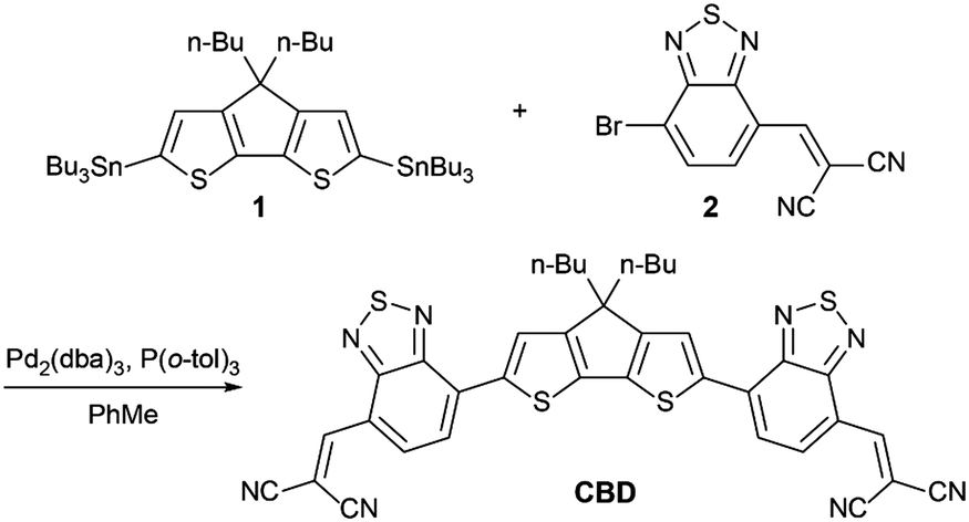
The synthesis route of CBD is depicted in Scheme 1. Compound 1 and 2 were reacted to offer the target molecule CBD using a Stille-coupling reaction in a yield of 61% as a dark blue solid. CBD was characterized in detail with 1H-NMR, 13C-NMR, and high-resolution mass spectrometry, which have been summarized in the ESI.‡ The results of the thermogravimetric analysis (TGA) under a nitrogen atmosphere (see Fig. S2, ESI‡) indicate the good thermal stability of CBD with a 5% weight loss at a temperature of 367 °C. The differential scanning calorimetry (DSC) measurement was also performed. As shown in Fig. S3 (see the ESI‡), there are no obvious endothermic and exothermic peaks observed in the curve within the scan range of 50–330 °C, which indicates that the crystallinity of CBD is relatively weak. The ultraviolet-visible-near infrared (UV-vis-NIR) absorption spectra of CBD in the chloroform solution and in the solid state are shown in Fig. S4 (see the ESI‡) and Fig. 1b, and the detailed parameters are listed in Table S3 (see the ESI‡). Due to the strong intramolecular charge transfer (ICT) effect, CBD exhibits a strong and broad absorption in the visible and NIR regions. The maximum absorption peak of the solution is located at 680 nm and the molar extinction coefficient (εmax) is calculated to be as high as 1.11 × 10⁵ M−1 cm−1. On the other hand, in the thin film, the maximum absorption peak is slightly bathochromically-shifted to 689 nm, but the absorption band is significantly broadened compared with that in the solution. The film shows a low Eoptg of 1.41 eV, which may be due to the intermolecular π–π stacking. These characters are beneficial for efficient light harvesting and are very promising for application as an active layer material in organic photovoltaic devices. Cyclic voltammetry (CV) measurements were executed to probe the electrochemical properties of the CBD film (Fig. S5, ESI‡). After internal calibration of the potential using the ferrocene/ferrocenium (Fc/Fc+) redox couple, it was calculated that the EA and IP are 3.84 and 5.42 eV, respectively (Fig. 1c).
 | ||
| Scheme 1 Synthetic route for the small molecule CBD. | ||
 | ||
| Fig. 1 (a) Molecular structures of the donor DTDCTB and the acceptor CBD. (b) UV-vis-NIR absorption spectra. (c) EA and IP of the DTDCTB and CBD films and (d) device structure of the VD-SMSCs based on DTDCTB and CBD. | ||
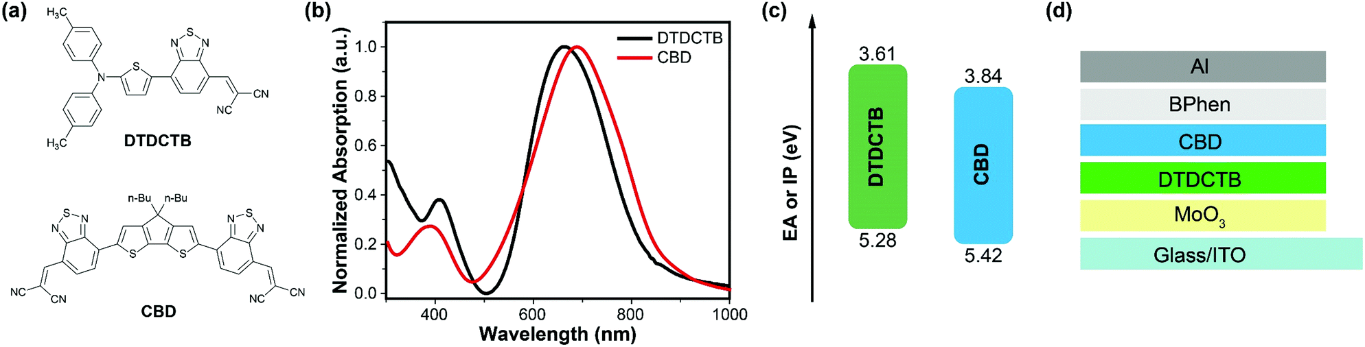
To evaluate the photovoltaic performance of this new vacuum-processable material, we constructed VD-SMSCs by matching them with DTDCTB, a donor material previously reported by Wong et al. (molecular structure shown in Fig. 1a).29 The two materials can take advantage of photons in the range of 300–880 nm, and their EA and IP values are well-matched, which provides a sufficient driving force for exciton dissociation (Fig. 1b and c). The vacuum-deposited devices adopted a PHJ structure of ITO/MoOx (5 nm)/DTDCTB/CBD/BPhen (10 nm)/Al (100 nm), where ITO is indium tin oxide, which serves as the transparent anode, and MoOx and BPhen were applied as the hole-transporting layer and electron-transporting layer, respectively (as shown in Fig. 1d). The organic materials used in the devices were all purified using temperature-gradient sublimation under vacuum conditions, after which all the layers were vacuum-deposited onto the substrate at room temperature. The photovoltaic performance was optimized by tuning the layer thicknesses of DTDCTB and CBD precisely. We firstly fixed the thickness of CBD at 20 nm, and varied the thickness of DTDCTB within the range of 5–30 nm (5, 10, 20, and 30 nm) to determine the optimal donor/acceptor thickness ratio (Fig. S6a and Table S4, ESI‡). With the thickness of DTDCTB increasing, Voc, Jsc and FF all increased at first and then decreased, among which the former two parameters reached their maximum values at a thickness of 10 nm, while for FF this was at 20 nm, and the overall performance reached the maximum value at a donor/acceptor thickness ratio of 1![[thin space (1/6-em)]](https://www.rsc.org/images/entities/char_2009.gif) :2. Then according to the optimal ratio, the total active layer thickness was further optimized (Table 1 and Fig. S6b, ESI‡). The best performance was achieved when the thicknesses of DTDCTB and CBD were 10 nm and 20 nm, respectively. Fig. 2a displays the current density–voltage (J–V) characteristics for the optimal DTDCTB/CBD-based VD-SMSC. Under AM 1.5G (intensity of 100 mW cm−2) illumination, the best PCE is 0.86% with a Voc of 0.78 V, a Jsc of 2.93 mA cm−2 and an FF of 37.58%. The Eloss of this optimal device is only 0.63 eV, which is attributed to the fact that the D–A strategy can adjust the energy levels flexibly, and reduce the energy offset between CBD and DTDCTB, thus making the energy levels of the two materials form a suitable alignment, and benefiting Eloss reduction. The storage stability of the optimized PHJ device without any encapsulation was also investigated as shown in Fig. S7 (see the ESI‡). During the two-week test period, the Voc remained basically unchanged, Jsc decreased but FF increased, and the final PCE changed very little. The relevant external quantum efficiency (EQE) curve is shown in Fig. 2b. The device exhibits a broad EQE response in the wavelength region from 300 to 880 nm, with a maximum value of 14.9% at 770 nm, which is consistent with the absorption wavelength range of the active layer materials, and indicates that the excitons generated by CBD could indeed move to the interface of DTDCTB/CBD, and then dissociate into free charges, which further transport to the electrodes and are collected, thus contributing to the final Jsc. The Jsc offered by the integration of the EQE curve is 2.86 mA cm−2, which is well-matched with the result of the J–V tests with an error within 3%, and indicates that the measurement of performance is reliable.
:2. Then according to the optimal ratio, the total active layer thickness was further optimized (Table 1 and Fig. S6b, ESI‡). The best performance was achieved when the thicknesses of DTDCTB and CBD were 10 nm and 20 nm, respectively. Fig. 2a displays the current density–voltage (J–V) characteristics for the optimal DTDCTB/CBD-based VD-SMSC. Under AM 1.5G (intensity of 100 mW cm−2) illumination, the best PCE is 0.86% with a Voc of 0.78 V, a Jsc of 2.93 mA cm−2 and an FF of 37.58%. The Eloss of this optimal device is only 0.63 eV, which is attributed to the fact that the D–A strategy can adjust the energy levels flexibly, and reduce the energy offset between CBD and DTDCTB, thus making the energy levels of the two materials form a suitable alignment, and benefiting Eloss reduction. The storage stability of the optimized PHJ device without any encapsulation was also investigated as shown in Fig. S7 (see the ESI‡). During the two-week test period, the Voc remained basically unchanged, Jsc decreased but FF increased, and the final PCE changed very little. The relevant external quantum efficiency (EQE) curve is shown in Fig. 2b. The device exhibits a broad EQE response in the wavelength region from 300 to 880 nm, with a maximum value of 14.9% at 770 nm, which is consistent with the absorption wavelength range of the active layer materials, and indicates that the excitons generated by CBD could indeed move to the interface of DTDCTB/CBD, and then dissociate into free charges, which further transport to the electrodes and are collected, thus contributing to the final Jsc. The Jsc offered by the integration of the EQE curve is 2.86 mA cm−2, which is well-matched with the result of the J–V tests with an error within 3%, and indicates that the measurement of performance is reliable.
| D/A thickness [nm] | V oc [V] | J sc [mA cm−2] | FFa [%] | PCEa [%] |
|---|---|---|---|---|
| a All the average values with standard deviations were calculated from over 10 independent devices. | ||||
| 5/10 | 0.79 | 2.69 | 33.49 | 0.71 |
| (0.79 ± 0.01) | (2.67 ± 0.02) | (33.45 ± 0.07) | (0.70 ± 0.05) | |
| 10/20 | 0.78 | 2.93 | 37.58 | 0.86 |
| (0.78 ± 0.01) | (2.89 ± 0.03) | (37.24 ± 0.27) | (0.85 ± 0.02) | |
| 20/40 | 0.77 | 2.55 | 33.86 | 0.67 |
| (0.77 ± 0.01) | (2.53 ± 0.04) | (37.75 ± 0.15) | (0.66 ± 0.01) | |
 | ||
| Fig. 2 (a) J–V characteristics and (b) EQE curve for the optimal VD-SMSC based on DTDCTB and CBD under AM 1.5G (100 mW cm−2) illumination. The inset graph in (a) is a photograph of the optimal device and the effective area is 0.09 cm2. | ||
However, the device suffers from a relatively low Jsc and FF, which has a significant correlation with the probability of the exciton dissociation and charge collection (P(E,T)), the charge transport ability and the degree of charge recombination. The relationship between photocurrent density (Jph) and effective voltage (Veff) was first measured, where Jph is the difference between photocurrent density under AM 1.5G illumination (JL) and the dark current density obtained under dark conditions (JD), and Veff is defined as V0 − Vapp (V0 is the voltage when JL = JD and Vapp is the applied voltage). P(E,T) is obtained by Jph/Jsat, where Jsat is the saturation photocurrent density. As displayed in Fig. S8 (see the ESI‡), Jph exhibits a pronounced field-dependent behaviour in the entire Veff region, which indicates a relatively low P(E,T), that is, the photogenerated excitons cannot be completely dissociated into free charges, which may be due to poor exciton migration or severe donor–acceptor interface recombination. Then, to study the charge recombination behaviour of the device, the dependence of Voc and Jsc on light intensity (Plight) were also measured (Fig. S9, ESI‡).30–32 The slope of Vocversus lnPlight evaluates the degree of trap-assisted recombination. A slope of 2kBT/e states that trap-assisted recombination is the dominant recombination mechanism in the device while the slope of kBT/e indicates that bimolecular recombination is dominant, where kB is the Boltzmann constant and T is the Kelvin temperature. In this CBD-based VD-SMSC, the slope is 1.52kBT/e. The relationship between Jsc and Plight can be expressed using the formula of Jsc ∝ Pαlight, where α is the exponential factor. If all the charges are swept out and collected without any bimolecular recombination, the value of α should be 1. The α is 0.87 in this optimal VD-SMSC. The recombination analysis demonstrates that the free charges generated by those excitons that can be dissociated successfully also encounter trap-assisted or bimolecular recombination during the charge transport process, which will cause the loss of free carriers, and affects the number of carriers that can be finally collected by the electrodes and lead to the loss of Jsc. Meanwhile, the FF, which is a factor that represents competition between sweep-out of the photogenerated carriers and the recombination of carriers, will also decrease. The vertical charge transport ability of the pristine CBD film was also investigated using the space-charge limited current (SCLC) method (Fig. S10, ESI‡), and the electron mobility (μe) was calculated to be 3.38 × 10⁻⁶ cm2 V−1 s−1. Since the charge transport ability of the film is related to the molecular stacking, grazing-incidence wide-angle X-ray scattering (GIWAXS) was applied to investigate the molecular crystallinity in the pristine CBD films as shown in Fig. S11 (see the ESI‡). From the two-dimensional (2D) pattern, the pristine CBD film shows a broad amorphous halo, and from the corresponding 1D line-cut profiles, CBD shows wide (010) π–π stacking peaks both in the out-of-plane (OOP) and in-plane (IP) directions, which indicates that CBD adopts both face-on and edge-on orientations in the vacuum-deposited film. The crystal coherence length (CCL) values are calculated to be only 1.12 and 1.43 nm in the IP and OOP directions, which indicates weak structural order. Moreover, the charge carrier mobilities in the optimized PHJ device have also been investigated as shown in Fig. S10 (see the ESI‡). The hole mobility (μh) and μe were calculated to be 1.15 × 10⁻⁶ and 1.04 × 10⁻⁶ cm2 V−1 s−1, respectively. The relatively low mobilities can lead to charge recombination and greatly influence the final performance. From all the above analyses, the reasons for the relatively low Jsc and FF is well explained.
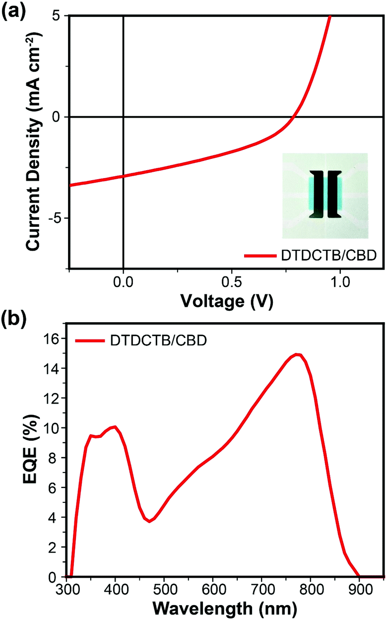
The surface morphology of the DTDCTB and DTDCTB/CBD sublimated films was characterized using the atomic force microscope (AFM) operating in tapping mode. As shown in Fig. 3a, DTDCTB forms a smooth and homogeneous layer on the substrate (ITO/MoOx) without any obvious aggregates and the root-mean-square (RMS) value of this film is 4.30 nm, which indicates its moderate crystallinity. Different from the film formed by the strong crystalline material α-6T, of which the RMS value is up to 10.1 nm, which is accompanied by some spike-like peaks with a height of over 60 nm,33,34 the smooth surface of the DTDCTB film cannot provide a sufficient contact surface for the subsequent deposited CBD film, which is also a factor limiting the performance to a certain extent. Fig. 3b shows the AFM image of the CBD film grown on the DTDCTB film. The CBD film is also uniform and continuous and covers the DTDCTB layer completely, and evenly distributed larger domains are observed. The lower RMS value of 3.05 nm indicates that the film exhibits a relatively low crystallinity, which is unfavourable for charge transport, but can form a good contact with the Bphen and electrode, which benefits charge collection.
 | ||
| Fig. 3 Surface morphology characterization using AFM height images of (a) DTDCTB and (b) DTDCTB/CBD sublimated films (scan area: 3.0 μm × 3.0 μm). | ||
In summary, considering the prominent advantages of NFAs and their success in boosting the performance of solution processed SMSCs as well as the promising prospects of vacuum deposition technology in the commercialization of OSCs, a new A–A′–D–A′–A-structured NFA CBD was designed and synthesized using the D–A strategy for application in VD-SMSCs for the first time. The properties of CBD were fully characterized. CBD exhibits good thermal stability and a low molar weight but a high molar extinction coefficient, which is favourable for vacuum-deposition and light harvesting. Also, the CBD film shows a strong and broad absorption in the visible and NIR regions due to the strong ICT effect, which corresponds to a low Eoptg of 1.41 eV, and an IP and EA of 5.42 eV and 3.84 eV, respectively. By applying DTDCTB as the donor and CBD as the acceptor, VD-SMSCs with a PHJ structure were constructed and the optimal device yielded a PCE of 0.86% with a Voc of 0.78 V, a Jsc of 2.93 mA cm−2 and an FF of 37.58%, accompanied by a low Eloss of 0.63 eV. This work demonstrates the great application potential of D–A-type NFAs in VD-SMSCs. In our device, there is still room for further improvement of the Jsc and FF values. Further design of NFAs with higher crystallinity, for example, to enhance the molecular co-planarity, or to shorten the alkyl chain to make the molecules stack more compactly, is of great importance. Also, improvement of device processing, including device structure optimization and the adoption of substrate heating, is urged, which is beneficial for higher Jsc and FF values.
Conflicts of interest
There are no conflicts to declare.Acknowledgements
The authors thank the National Key R&D Program of China (2019YFA0705900, 2017YFA0204701) and the National Natural Science Foundation of China (21572234, 21661132006, 91833304) for their financial support.References
- G. Li, R. Zhu and Y. Yang, Nat. Photonics, 2012, 6, 153–161 CrossRef CAS.
- C. Brabec, U. Scherf and V. Dyakonov, Organic Photovoltaics: Materials, Device Physics, and Manufacturing Technologies, Wiley-VCH Verlag GmbH & Co. KGaA, Weinheim, Germany, 2nd edn, 2014 Search PubMed.
- L. Lu, T. Zheng, Q. Wu, A. M. Schneider, D. Zhao and L. Yu, Chem. Rev., 2015, 115, 12666–12731 CrossRef CAS PubMed.
- O. Inganäs, Adv. Mater., 2018, 30, 1800388 CrossRef.
- A. Mishra and P. Bäuerle, Angew. Chem., Int. Ed., 2012, 51, 2020–2067 CrossRef CAS PubMed.
- S. D. Collins, N. A. Ran, M. C. Heiber and T.-Q. Nguyen, Adv. Energy Mater., 2017, 7, 1602242 CrossRef.
- Y. Huo, H.-L. Zhang and X. Zhan, ACS Energy Lett., 2019, 4, 1241–1250 CrossRef CAS.
- C. W. Tang, Appl. Phys. Lett., 1986, 48, 183–185 CrossRef CAS.
- N. Li, Y. Kan, K. Gao, M. Zhang, N. Li, G. Zhou, S. B. Jo, X. Shi, F. Lin, Q. Rong, F. Liu, G. Zhou and A. K.-Y. Jen, Joule, 2020, 4, 2223–2226 CrossRef.
- J. Ge, L. Hong, W. Song, L. Xie, J. Zhang, Z. Chen, K. Yu, R. Peng, X. Zhang and Z. Ge, Adv. Energy Mater., 2021, 11, 2100800 CrossRef CAS.
- M. Jiang, H. Bai, H. Zhi, L. Yan, H. Y. Woo, L. Tong, J. Wang, F. Zhang and Q. An, Energy Environ. Sci., 2021, 14, 3945–3953 RSC.
- C. An, Y. Qin, T. Zhang, Q. Lv, J. Qin, S. Zhang, C. He, H. Ade and J. Hou, J. Mater. Chem. A, 2021, 9, 13653–13660 RSC.
- J. Zhang, H. Tan, X. Guo, A. Facchetti and H. Yan, Nat. Energy, 2018, 3, 720–731 CrossRef CAS.
- A. Wadsworth, M. Moser, A. Marks, M. S. Little, N. Gasparini, C. J. Brabec, D. Baran and I. McCulloch, Chem. Soc. Rev., 2019, 48, 1596–1625 RSC.
- Q. Yue, W. Liu and X. Zhu, J. Am. Chem. Soc., 2020, 142, 11613–11628 CrossRef CAS.
- Q. Burlingame, X. Huang, X. Liu, C. Jeong, C. Coburn and S. R. Forrest, Nature, 2019, 573, 394–397 CrossRef CAS.
- O. L. Griffith, X. Liu, J. A. Amonoo, P. I. Djurovich, M. E. Thompson, P. F. Green and S. R. Forrest, Phys. Rev. B: Condens. Matter Mater. Phys., 2015, 92, 085404 CrossRef.
- X. Che, X. Xiao, J. D. Zimmerman, D. Fan and S. R. Forrest, Adv. Energy Mater., 2014, 4, 1400568 CrossRef.
- Y.-H. Chen, L.-Y. Lin, C.-W. Lu, F. Lin, Z.-Y. Huang, H.-W. Lin, P.-H. Wang, Y.-H. Liu, K.-T. Wong, J. Wen, D. J. Miller and S. B. Darling, J. Am. Chem. Soc., 2012, 134, 13616–13623 CrossRef CAS PubMed.
- V. Steinmann, N. M. Kronenberg, M. R. Lenze, S. M. Graf, D. Hertel, K. Meerholz, H. Bürckstümmer, E. V. Tulyakova and F. Würthner, Adv. Energy Mater., 2011, 1, 888–893 CrossRef CAS.
- M. Zhang, H. Wang, H. Tian, Y. Geng and C. W. Tang, Adv. Mater., 2011, 23, 4960–4964 CrossRef CAS PubMed.
- A. Mishra, D. Popovic, A. Vogt, H. Kast, T. Leitner, K. Walzer, M. Pfeiffer, E. Mena-Osteritz and P. Bäuerle, Adv. Mater., 2014, 26, 7217–7223 CrossRef CAS.
- T.-y. Li, T. Meyer, Z. Ma, J. Benduhn, C. Körner, O. Zeika, K. Vandewal and K. Leo, J. Am. Chem. Soc., 2017, 139, 13636–13639 CrossRef CAS.
- K. Cnops, B. P. Rand, D. Cheyns, B. Verreet, M. A. Empl and P. Heremans, Nat. Commun., 2014, 5, 3406 CrossRef PubMed.
- I. Kim, H. M. Haverinen, Z. Wang, S. Madakuni, Y. Kim, J. Li and G. E. Jabbour, Chem. Mater., 2009, 21, 4256–4260 CrossRef CAS.
- K. Menekse, P. Chen, B. Mahlmeister, O. Anhalt, A. Kudzus, M. Stolte and F. Würthner, J. Mater. Chem. C, 2020, 8, 15303–15311 RSC.
- H. Yao, L. Ye, H. Zhang, S. Li, S. Zhang and J. Hou, Chem. Rev., 2016, 116, 7397–7457 CrossRef CAS.
- H. Tang, C. Yan, J. Huang, Z. Kan, Z. Xiao, K. Sun, G. Li and S. Lu, Matter, 2020, 3, 1403–1432 CrossRef.
- L.-Y. Lin, Y.-H. Chen, Z.-Y. Huang, H.-W. Lin, S.-H. Chou, F. Lin, C.-W. Chen, Y.-H. Liu and K.-T. Wong, J. Am. Chem. Soc., 2011, 133, 15822–15825 CrossRef CAS.
- M. M. Mandoc, F. B. Kooistra, J. C. Hummelen, B. de Boer and P. W. M. Blom, Appl. Phys. Lett., 2007, 91, 263505 CrossRef.
- S. R. Cowan, A. Roy and A. J. Heeger, Phys. Rev. B: Condens. Matter Mater. Phys., 2010, 82, 245207 CrossRef.
- S. R. Cowan, J. Wang, J. Yi, Y.-J. Lee, D. C. Olson and J. W. P. Hsu, J. Appl. Phys., 2013, 113, 154504 CrossRef.
- J. Sakai, T. Taima and K. Saito, Org. Electron., 2008, 9, 582–590 CrossRef CAS.
- V. C. Nikolis, J. Benduhn, F. Holzmueller, F. Piersimoni, M. Lau, O. Zeika, D. Neher, C. Koerner, D. Spoltore and K. Vandewal, Adv. Energy Mater., 2017, 7, 1700855 CrossRef.
Footnotes |
| † Dedicated to the 80th birthday of Prof. Daoben Zhu. |
| ‡ Electronic supplementary information (ESI) available: Synthesis details and NMR spectra, details concerning device fabrication and characterization, TGA, DSC, and cyclic voltammogram measurements, Voc, and Jscvs. light intensity curves, Jphvs. Veff curve, and SCLC characteristics. See DOI: 10.1039/d1tc03954g |
| § These authors contributed equally to this work. |
| This journal is © The Royal Society of Chemistry 2022 |