
Self-assembled dipoles of o-carborane on gate oxide tuning charge carriers in organic field effect transistors†‡
Ming
Chu
a,
Jie
Zhang
a,
Xingwei
Zeng
a,
Zefeng
Chen
b,
Danqing
Liu
 c,
Han
Chen
a,
Zuowei
Xie
a,
Jianbin
Xu
b and
Qian
Miao
*a
c,
Han
Chen
a,
Zuowei
Xie
a,
Jianbin
Xu
b and
Qian
Miao
*a
aDepartment of Chemistry, The Chinese University of Hong Kong, New Territories, Shatin, Hong Kong, China. E-mail: miaoqian@cuhk.edu.hk
bDepartment of Electronic Engineering, The Chinese University of Hong Kong, New Territories, Shatin, Hong Kong, China
cShenzhen Key Laboratory of Polymer Science and Technology, College of Materials Science and Engineering, Shenzhen University, Shenzhen, 518060, China
First published on 23rd August 2021
Abstract
Molecules of 12-o-carboranyldodecylphosphonic acid form a novel self-assembled monolayer (SAM) on alumina, which can effectively tune charge carriers in organic field effect transistors (OFETs) with the assembled dipoles of o-carborane at the semiconductor–dielectric interface. This SAM has not only realized p-channel OFETs of pentacene with both low threshold voltage and high field effect mobility (up to 5.2 cm2 V−1 s−1), but also enabled ambipolar charge transport in the solution-processed thin films of a chlorinated tetraazapentacene, which is a typical n-type organic semiconductor. As measured with Kelvin probe force microscopy, the SAM of CBPA has a surface electrostatic potential of −0.40 ± 0.10 V versus gold, which is in agreement with the observed shift of threshold voltage in the OFETs.
Introduction
Self-assembled monolayers (SAMs) are two-dimensional molecular assemblies of organic molecules forming spontaneously on a variety of surfaces by chemisorption, which involves a chemical reaction between the surface and the adsorbed molecules.1 Owing to the unique capability of manipulating surface properties dramatically, SAMs have been developed as a powerful molecular platform2–5 for interface engineering6–8 of organic field effect transistors (OFETs), which are basically interface devices with their performance strongly relying on the structures and properties of device interfaces. Polar terminal groups in a SAM on the dielectric surface of an OFET give rise to surface dipoles, which provide an electrical field in addition to the applied gate bias. This additional field is able to control charge carrier density at the semiconductor–dielectric interface. Since Iwasa's pioneering study on using the SAM of fluorinated alkyl silane to accumulate holes in the OFET conduction channel,9 a few polar terminal groups on the SAM-modified dielectric surface have shown their capability to control the threshold voltage and turn-on voltage of OFETs.10–13 It is worth noting that the polar terminal groups in a SAM not only result in surface dipoles but also determine surface energy, which is of key importance to the growth of organic semiconductor films on the dielectric surface14 either through vacuum deposition or a solution-based process. In fact, introduction of polar terminal groups to a SAM-modified dielectric surface in an OFET to control its threshold voltage often leads to deterioration of charge transport as a result of impairing the molecular packing and film morphology of organic semiconductors.10,11,13 SAMs that can effectively control threshold voltage with a polar terminal group and simultaneously achieve high field effect mobility are still rare.Herein, we report a novel SAM formed by 12-o-carboranyldodecylphosphonic acid (CBPA as shown in Fig. 1) on alumina, which has realized a p-channel OFET with both low threshold voltage and high field effect mobility and enabled ambipolar charge transport in the OFET of a typical n-type organic semiconductor. o-Carborane is an icosahedral boron hydride cluster in which two of the BH vertices are replaced by CH units giving rise to a dipole moment as large as 4.53 Debye.15 Alignment of the dipoles of o-carborane in a SAM can result in a large surface dipole for different applications. The SAMs of o-carboranethiols on gold16,17 and other metal18 surfaces have been reported to control liquid crystal alignment,19 to modulate charge transport across molecular junctions,20 and to adjust the surface work function of metal.21 On the other hand, the SAMs of o-carborane on non-metal surfaces remain unexplored, and this work, to the best of our knowledge, is the first study on the SAMs o-caborane on metal oxides.
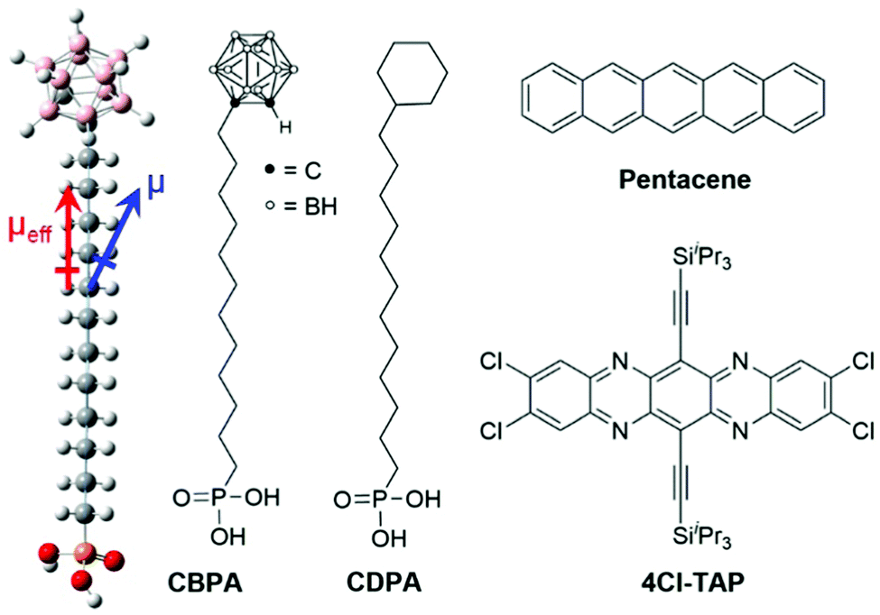 | ||
| Fig. 1 Molecular structures of phosphonic acids and organic semiconductors for this study. The dipoles of CBPA direct from the positive end to the negative end. | ||
As shown in Fig. 1, 12-o-carboranyldodecylphosphonic acid (CBPA) is designed to have phosphonic acid attached to o-carborane through a long alkyl chain because long-chain phosphonic acids are well known to efficiently bind to metal oxides with stable P–O–M phosphonate bonds resulting in ordered and densely packed SAMs.22–24 Due to the large dipole moment of o-carborane, CBPA has a dipole moment (μ) of 4.61 Debye, which is calculated at the B3LYP level of the density functional theory (DFT) with the 6-31++G(d,p) basis, and has an effective dipole moment (μeff) of 3.58 Debye from the phosphonic acid end to the carborane end along the direction of the carbon chain as shown in Fig. 1. In comparison to CBPA, organosilanes,9 carboxylic acids12 and phosphonic acids13 that were used for interface engineering of OFETs with their surface dipoles possess smaller effective dipole moments in absolute value. For example, the calculated absolute value of the effective dipole moment is 0.98 Debye for [3-(N,N′-3-dimethylamino)propyl]triethoxysilane25 and 2.27 Debye for pentadecafluoro-octadecylphosphonic acid.13
In order to study how the SAM of CBPA modulates charge carriers in OFETs, two organic semiconductors with high field effect mobility were selected for this study, and the SAM of 12-cyclohexyldodecylphosphonic acid (CDPA in Fig. 1)26 was used as a reference. One semiconductor is pentacene, a benchmark for p-type organic semiconductors, and the other is 2,3,9,10-tetrachloro-6,13-(bis(triisopropylsilyl)ethynyl)-5,7,12,14-tetraazapentacene (4Cl-TAP),27 which represents solution-processed n-type organic semiconductors. Moreover, CDPA has been demonstrated by us to provide an ordered dielectric surface wettable by common organic solvents for high performance p- and n-channel OFETs.26,28–30 Detailed below are the synthesis of CBPA, the characterization of the SAM of CBPA on alumina, and the effects of the SAM of CBPA on modulating charge carriers in the OFETs of pentacene and 4Cl-TAP.
Results and discussion
CBPA was synthesized from o-carborane (1) as shown in Scheme 1. Treatment of 1 with one equivalent of n-butyllithium resulted in 1-lithio-o-carborane,31,32 which reacted with the added 1,12-dibromododecane giving Br-functionalized carborane 2. The reaction of 2 with triethyl phosphite afforded diethyl phosphonate 3. The hydrolysis of 3 gave pure CBPA in a low yield (12%) as a result of loss during the work-up process, which involved formation of emulsion and precipitation from a solution in CH2Cl2 by addition of a poor solvent (hexane). To facilitate fabrication of OFETs, a thin layer of alumina (AlOx) was deposited on a highly doped silicon wafer by spin-coating a solution of Al(NO3)3 in ethanol (0.5 mol L−1) onto the substrate and baking the resulting film at 300 °C to achieve complete decomposition of nitrate and a high degree of dehydration.28 After treatment with oxygen plasma, the AlOx-coated Si wafer was soaked into a solution of CBPA in isopropanol at room temperature for 12 hours to allow formation of the SAM. CBPA is a stable compound, and the CBPA-modified AlOx stored under ambient conditions for months can be used for fabrication of OFETs without leading to apparent degradation in device performance.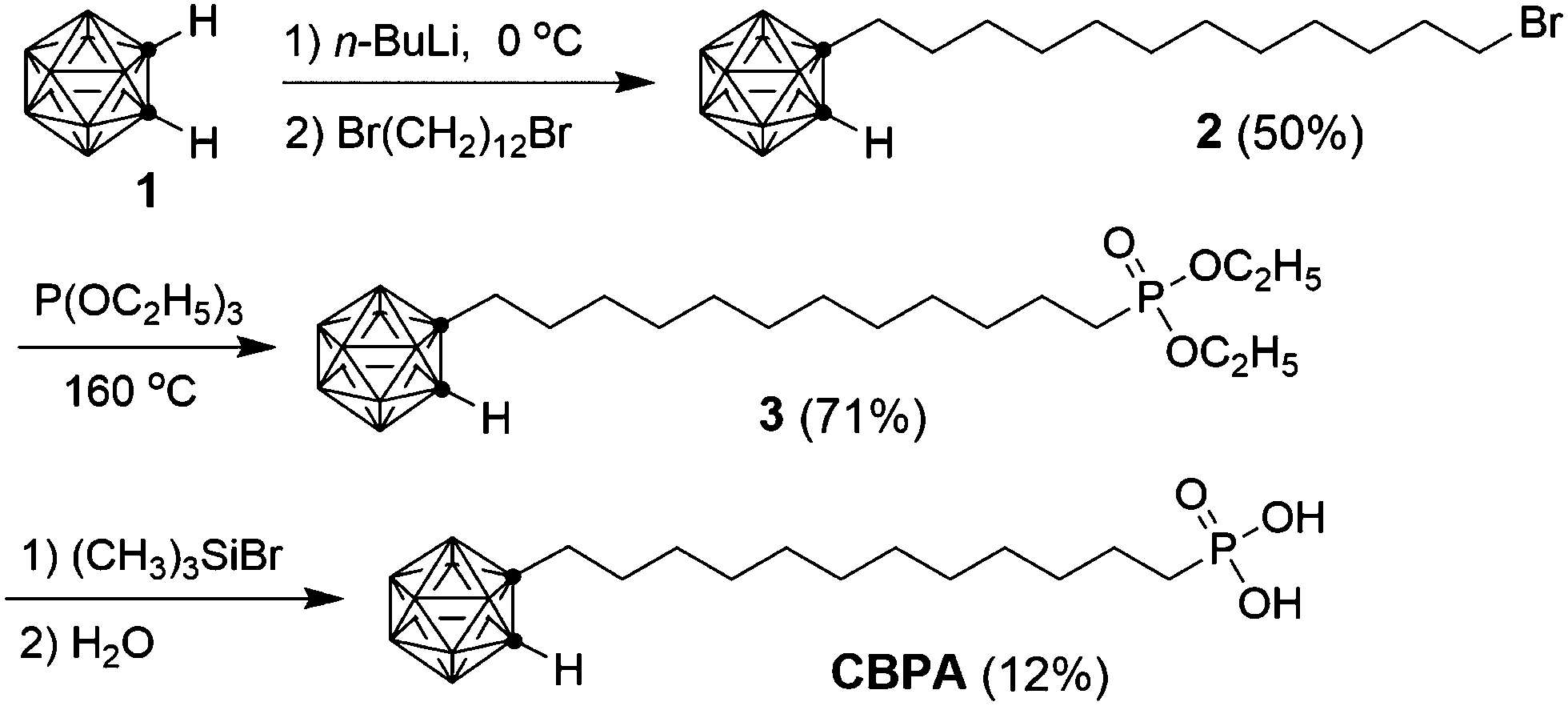 | ||
| Scheme 1 Synthesis of CBPA. | ||
The CBPA-modified AlOx dielectric was characterized in terms of surface composition, surface roughness, surface energy, capacitance, leakage current and surface potential using a variety of techniques, in comparison with the CDPA-modified AlOx. The surface composition of the SAM of CBPA was studied with core level X-ray photoelectron spectroscopy. The B (1s) spectrum can be fitted with three peaks that have binding energies of 189.5, 190.3 and 191.6 eV with a ratio of 2![[thin space (1/6-em)]](https://www.rsc.org/images/entities/char_2009.gif) :2:1 as shown in Fig. S13a in the ESI,‡ revealing boron atoms in three bonding environments. This result is in agreement with the three types of boron atoms (B2–B, BC–B and C2–B) in o-carborane, and is similar to those reported for the chemical vapor deposited films of o-carborane.33,34 The C (1s) spectrum (Fig. S13b, ESI‡) reveals three types of carbon atoms with binding energies of 284.8, 285.3 and 287.1 eV, which can be attributed to carbon atoms bonded to boron, carbon and phosphorus, respectively. With the atomic sensitivity factors of boron and carbon taken into consideration, the C/B ratio in the SAM of CBPA is calculated as 1.3, which is in agreement with the numbers of carbon(14) and boron(10) atoms in the molecule of CBPA. Atomic force microscopy (AFM) reveals that the SAM of CBPA has a very smooth surface with a root mean square roughness (RMS) of 0.09 nm in an area of 4 μm2, which is smaller than that of CDPA (0.18 nm). By measuring the contact angles of the SAM with two probe liquids (distilled water and CH2I2),35 the surface energy of the SAM of CBPA is determined as 40.7 mN m−1 consisting of a polar component of 3.7 mN m−1 and a dispersion component of 37.0 mN m−1. In comparison to CBPA, the SAM of CDPA has a smaller surface energy (31.6 mN m−1) consisting of a polar component of 0.3 mN m−1 and a dispersion component of 31.3 mN m−1. The larger surface energy of CBPA is in agreement with the fact the o-carboranyl group in CBPA has a much large dipole moment and more delocalized electrons than the cyclohexyl group in CDPA. The average capacitance per unit area (Ci) of CBPA-modified AlOx was measured as 147 ± 11 nF cm−2 from a metal–insulator–metal structure, which had CBPA-AlOx sandwiched between electrodes of highly doped silicon and vacuum-deposited gold, at a frequency of 100 Hz.36,37 The value of Ci allowed the OFETs to be operated with a gate voltage as low as 3 volts.38
:2:1 as shown in Fig. S13a in the ESI,‡ revealing boron atoms in three bonding environments. This result is in agreement with the three types of boron atoms (B2–B, BC–B and C2–B) in o-carborane, and is similar to those reported for the chemical vapor deposited films of o-carborane.33,34 The C (1s) spectrum (Fig. S13b, ESI‡) reveals three types of carbon atoms with binding energies of 284.8, 285.3 and 287.1 eV, which can be attributed to carbon atoms bonded to boron, carbon and phosphorus, respectively. With the atomic sensitivity factors of boron and carbon taken into consideration, the C/B ratio in the SAM of CBPA is calculated as 1.3, which is in agreement with the numbers of carbon(14) and boron(10) atoms in the molecule of CBPA. Atomic force microscopy (AFM) reveals that the SAM of CBPA has a very smooth surface with a root mean square roughness (RMS) of 0.09 nm in an area of 4 μm2, which is smaller than that of CDPA (0.18 nm). By measuring the contact angles of the SAM with two probe liquids (distilled water and CH2I2),35 the surface energy of the SAM of CBPA is determined as 40.7 mN m−1 consisting of a polar component of 3.7 mN m−1 and a dispersion component of 37.0 mN m−1. In comparison to CBPA, the SAM of CDPA has a smaller surface energy (31.6 mN m−1) consisting of a polar component of 0.3 mN m−1 and a dispersion component of 31.3 mN m−1. The larger surface energy of CBPA is in agreement with the fact the o-carboranyl group in CBPA has a much large dipole moment and more delocalized electrons than the cyclohexyl group in CDPA. The average capacitance per unit area (Ci) of CBPA-modified AlOx was measured as 147 ± 11 nF cm−2 from a metal–insulator–metal structure, which had CBPA-AlOx sandwiched between electrodes of highly doped silicon and vacuum-deposited gold, at a frequency of 100 Hz.36,37 The value of Ci allowed the OFETs to be operated with a gate voltage as low as 3 volts.38
The electrostatic potential (USAM) of CBPA- and CDPA-modified AlOx was measured with Kelvin probe force microscopy (KPFM). Because KPFM measures the contact-potential difference between the surface and the probe tip,39–41 quantitative determination of the electrostatic potential independent of tip requires using a surface reference, which was gold in this study. Fig. 2a shows the representative AFM topography, KPFM electrostatic potential map and a line scan of the SAM of CBPA, and Fig. 2b shows those of the SAM of CDPA for comparison. As measured from 40 line scans at different areas on three SAMs, the electrostatic potential of the SAM of CBPA is determined as −0.40 ± 0.10 V versus gold, and that of CDPA is determined as 0.17 ± 0.14 V versus gold. The opposite signs of the electrostatic potentials of the two SAMs are in agreement with the calculated effective dipole moments of CBPA (3.58 Debye) and CDPA (−0.65 Debye) along the direction of their carbon chain.
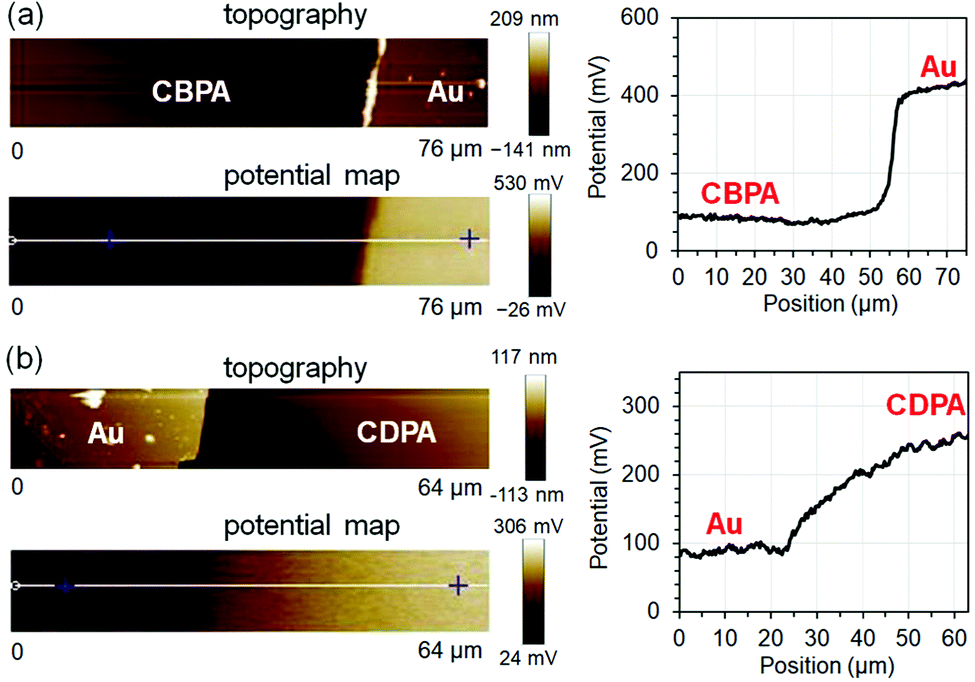 | ||
| Fig. 2 Representative AFM topography image, KPFM electrostatic potential map and line scan (along the white line in the potential map) for the SAMs of CBPA (a) and CDPA (b). | ||
Unlike the known SAMs of fluorinated alkylphosphonic acids having poor wettability toward many organic solvents,11 the SAM of CBPA is wettable by common organic solvents and thus suitable for solution-based process. To fabricate OFETs, films of pentacene and 4Cl-TAP were vacuum-deposited and dip-coated, respectively, onto the CBPA- and CDPA-modified AlOx as detailed in the ESI,‡ and gold was thermally evaporated in vacuum onto the organic semiconductor films to form top-contact drain and source electrodes. The films of pentacene on CBPA exhibited four X-ray diffraction (XRD) peaks (Fig. S16, ESI‡), which correspond to a thin film polymorph of pentacene with interlayer spacing d(001) of 15.6 Å.42 In contrast, the films of pentacene on CDPA exhibited two sets of XRD peaks, which correspond to two thin film polymorphs of pentacene with interlayer spacing d(001) of 15.6 Å and 14.6 Å, respectively. AFM revealed that the vacuum-deposited films of pentacene on CBPA and CDPA consisting of grains with distinct terraces as shown in Fig. 3. The grains in the films on CBPA, with a size over 2 μm, are larger than those in the films on CDPA presumably because the SAM of CBPA with higher surface energy favors two-dimensional, or layer-by-layer growth.43,44 The dip-coated films of 4Cl-TAP on CBPA and CDPA exhibited similar XRD peaks, which are in accordance with the single crystal structure of 4Cl-TAP27 and suggest edge-on orientation of 4Cl-TAP molecules on the dielectric surface. AFM revealed that the dip-coated films of 4Cl-TAP on CBPA and CDPA consisting of flat ribbons (Fig. 3). The ribbons of 4Cl-TAP on CBPA are more than 15 μm wide while those on CDPA are about 2 μm wide, likely as a result of the larger surface energy of the SAM of CBPA.45 The AFM section analysis (Fig. S17 in the ESI‡) showed that the ribbons of 4Cl-TAP on CBPA are 34 to 38 nm thick, while the section analysis may not reflect the real thickness of the ribbons of 4Cl-TAP on CDPA because the gap between ribbons is not clear.
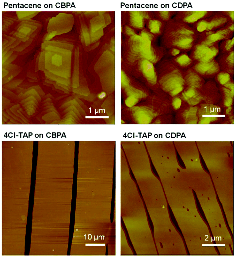 | ||
| Fig. 3 AFM images of pentacene films vacuum-deposited on CBPA- and CDPA-modified AlOxsubstrates and 4Cl-TAP films dip-coated on CBPA- and CDPA-modified AlOx. | ||
The films of pentacene on the SAMs of CBPA and CDPA both behaved as p-channel transistors. Fig. 4 shows the transfer I–V curves measured in air from the best performing transistors of pentacene on CBPA- and CDPA-modified AlOx, respectively. The field effect mobility in the saturation regime was extracted from these curves using the equation: IDS = (μWCi/2L)(VGS − Vth)2, where IDS is the drain current, μ is field effect mobility, Ci is the capacitance per unit area for the SAM-modified AlOx, W is the channel width, L is the channel length, and VGS and Vth are the gate and threshold voltage, respectively. As summarized in Table 1, the OFETs of pentacene on CBPA and CDPA exhibited similar field effect mobilities but very different threshold voltage. The similar mobilities indicate that the different film crystallinities and morphologies on the two SAMs are not the limiting factors for charge transport. The threshold voltage apparently shifts from −0.10 ± 0.22 V to −1.62 ± 0.23 V when CBPA is replaced by CDPA in the transistors, in agreement with the significant difference between the effective dipole moments of CBPA (3.58 Debye) and CDPA (−0.65 Debye) along the direction of their carbon chain. In comparison to the OFETs of pentacene on the CBPA and CDPA-modified AlOx, those on bare AlOx exhibited lower field effect mobility of 0.98 ± 0.64 cm2 V−1 s−1 and a threshold voltage of −1.73 ± 0.39 V as shown in Fig. S20 and Table S3 in the ESI.‡
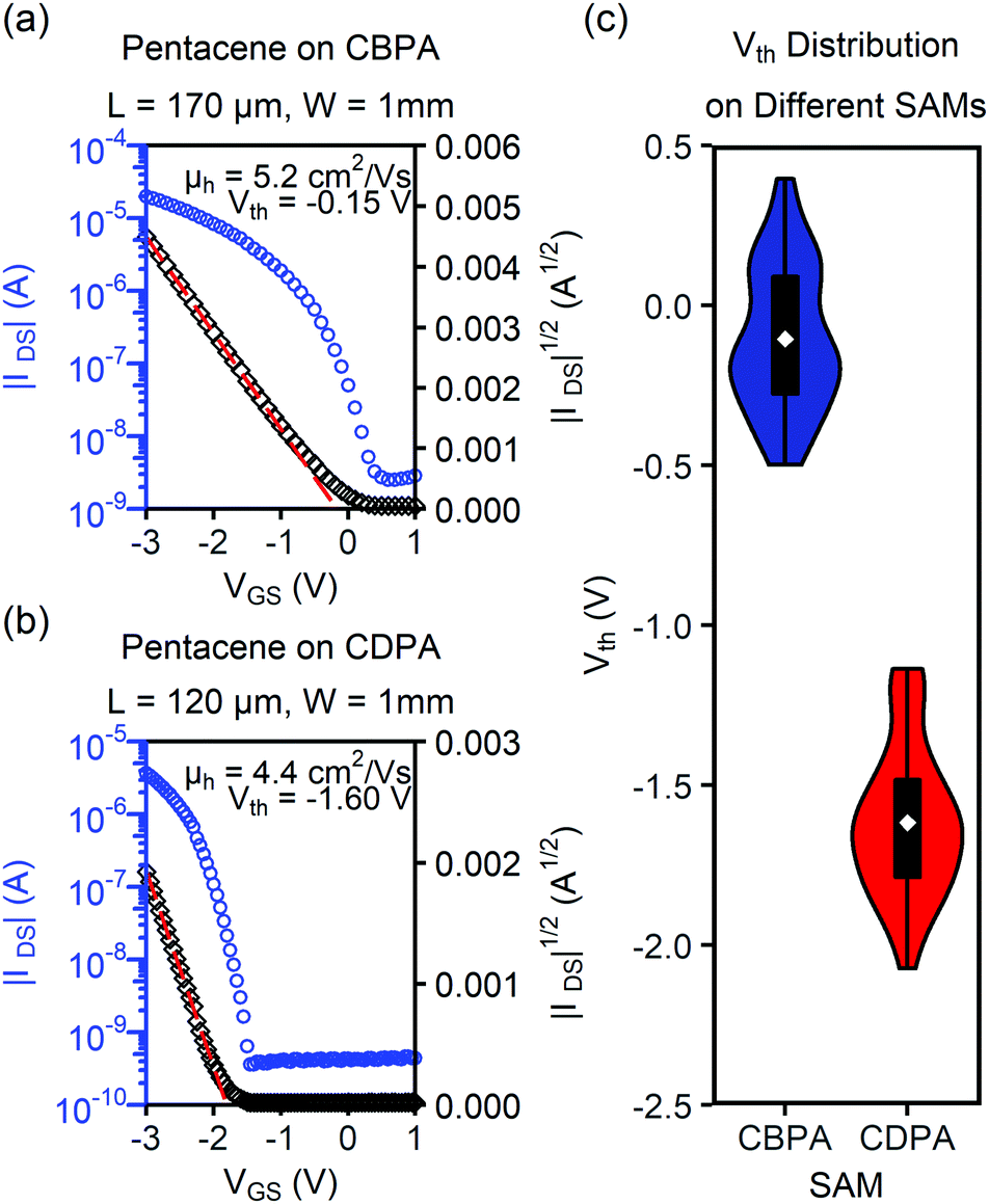 | ||
| Fig. 4 (a) Transfer I–V curves for the OFET of pentacene on CBPA with the highest field effect mobility; (b) transfer I–V curves for the OFET of pentacene on CDPA with the highest field effect mobility; (c) distribution of threshold voltage values for the OFETs of pentacene on CBPA- and CDPA-modified AlOx the white rhombus indicates the average value and the black bar indicates the interquatile range of the data. | ||
| μ FET (cm2 V−1 s−1) | V th (V) | |||
|---|---|---|---|---|
| Average | Highest | |||
| a Each average value for CBPA was obtained from at least 50 channels on 9 independent substrates, and each value for CDPA was obtained from at least 30 channels on 6 independent substrates. b Tested in air. c Tested in vacuum. d p-Channel performance. e n-Channel performance. | ||||
| Pentaceneb | CBPA | 2.3 ± 0.9 | 5.2 | −0.10 ± 0.22 |
| CDPA | 2.3 ± 1.0 | 4.4 | −1.62 ± 0.23 | |
| 4Cl-TAPc | CBPA (p)d | 0.20 ± 0.10 | 0.50 | −2.95 ± 0.40 |
| CBPA (n)e | 0.90 ± 0.47 | 1.6 | 2.76 ± 0.45 | |
| CDPA (n)e | 7.4 ± 2.8 | 13.9 | 1.17 ± 0.24 | |
Interestingly, the transistors of 4Cl-TAP on CBPA exhibited ambipolar charge transport although 4Cl-TAP is a typical n-type organic semiconductor. Fig. 5 shows the transfer I–V curves of the best performing OFET of 4Cl-TAP on CBPA with a drain voltage of −5.0 V and 5.0 V, respectively. The field effect mobility extracted from these I–V curves is 0.50 cm2 V−1 s−1 for holes and 1.5 cm2 V−1 s−1 for electrons. In contrast, the films of 4Cl-TAP on CDPA behaved as n-channel transistors with field effect mobility of up to 13.9 cm2 V−1 s−1, but did not show any p-channel field effect. To the best of knowledge, CBPA is the first SAM that enables ambipolar charge transport in a typical n-type small-molecule organic semiconductor although hydroxyl-free polymer dielectrics are well known to allow ambipolar charge transport in conjugated polymers in OFETs.46 As shown in Table 1, the threshold voltage of the n-channel OFETs of 4Cl-TAP shifts from 1.17 ± 0.24 V to 2.76 ± 0.45 V when CDPA is replaced by CBPA in the transistors. Both the direction and absolution value of this shift are in agreement with the threshold voltage shift for the OFETs of pentacene on CBPA and CDPA. The hole transport in the transistors of 4Cl-TAP on CBPA indicates that the surface dipole of the SAM of CBPA not only induces an extra gate bias but also helps to stabilize mobile holes in the active channel of transistor by electrostatic attractions. On the other hand, the surface dipole of CBPA impairs transport of electrons in the active channel by electrostatic repulsions. As a result, the field effect mobility of the transistors of 4Cl-TAP on CBPA is lower than that on CDPA by about one order of magnitude although the films on CBPA exhibit even better morphology than those on CDPA. It should also be noted that the field effect mobility of the transistors of 4Cl-TAP on CDPA herein is lower than that reported by us earlier27 presumably because the dielectric oxides and operation voltages are different. Moreover, the transfer I–V curves of the transistors of 4Cl-TAP on CDPA in this study (shown in Fig. S18e in the ESI‡) exhibited nearly ideal linear relationship between the square root of drain current and the gate voltage, while the transfer I–V curves of 4Cl-TAP as reported earlier exhibited deviation from the ideal straight line at higher gate bias by bending downward. Further study on the transistors of 4Cl-TAP fabricated on different dielectric surfaces is in progress in our laboratory.
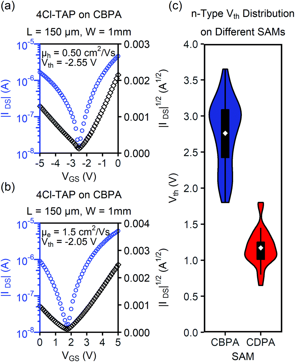 | ||
| Fig. 5 (a) Transfer I–V curves for the best performing OFET of 4Cl-TAP on CBPA with a drain voltage of −5.0 V for p-channel; (b) transfer I–V curves for the same OFET with a drain voltage of 5.0 V for n-channel; (c) distribution of threshold voltage values for the n-channel OFETs of 4Cl-TAP on CBPA- and CDPA-modified AlOx (the white rhombus indicates the average value and the black bar indicates the interquatile range of the data). | ||
To better understand the influence of the surface electrostatic potential on the threshold voltage shift, the threshold voltage shift was calculated on the basis of electrostatic measurements11 and compared with the experimental value measured from the OFETs. The gate potential induced by the SAM (VSAM) can be calculated from VSAM = CSAMUSAM/Ctotal.11,13 Here, USAM is the electrostatic potential of the SAM, which was measured by KPFM as the surface potential relative to gold, CSAM is the capacitance per unit area of the SAM, Ctotal is the total capacitance per unit area of the SAM-modified AlOx.47 Due to difficulties in direct measurement of the capacitance of a monolayer of molecules, CSAM was determined from Ctotal and the capacitance per unit of AlOx (CAlOx) on the basis of 1/Ctotal = 1/CAlOx + 1/CSAM. The measured values of USAM and Ctotal for CBPA-AlOx and CDPA-AlOx are summarized in Table 2, and the measured value of CAlOx is 181 ± 13 nF cm−2. On the basis of the above two equations, VSAM is calculated as −2.13 ± 1.21 V for CBPA and 0.81 ± 0.78 V for CDPA. As a result, the difference between the threshold voltages of the OFETs fabricated on the two SAMs is calculated as ΔVth = −(VCBPA − VCDPA) = 2.94 ± 1.44 V, which is in agreement with the experimentally measured threshold voltage shifts, 1.51 ± 0.32 V for the p-channel transistors of pentacene and 1.59 ± 0.53 V for the n-channel transistors of 4Cl-TAP.
| SAM | U SAM (V) | C total (nF cm−2) | C SAM (nF cm−2) | V SAM (V) |
|---|---|---|---|---|
| a Relative to gold as measured by KPFM. b Measured from 36 and 48 independent metal–insulator–metal devices for CBPA and CDPA, respectively. c Calculated on the basis of 1/CSAM = 1/Ctotal − 1/CAlOx. d Calculated from VSAM = CSAM·USAM/Ctotal. | ||||
| CBPA | −0.40 ± 0.10 | 147 ± 11 | 783 ± 395 | −2.13 ± 1.21 |
| CDPA | 0.17 ± 0.14 | 143 ± 12 | 681 ± 329 | 0.81 ± 0.78 |
Conclusions
In conclusion, the assembled dipoles of o-carborane in the SAM of CBPA on gate oxide allow effective tuning of charge carriers in OFETs. The SAM of CBPA has not only reduced the threshold voltage of the p-channel OFET of pentacene without sacrificing its high field effect mobility (up to 5.2 cm2 V−1 s−1), but also enabled ambipolar charge transport in the solution-processed films of 4Cl-TAP, a typical n-type organic semiconductor. The observed shift of threshold voltage in the OFETs is in agreement with the surface electrostatic potential measured by KPFM. This study demonstrates a new application of o-carborane for organic electronic devices. Unlike grafting electron-withdrawing o-carborane to an organic semiconductor molecule with covalent bonds to facilitate electron transport by lowering its LUMO energy level,48 the SAM of o-carborane at the semiconductor–dielectric interface accumulates holes in the conduction channel with high efficiency.Conflicts of interest
There are no conflicts to declare.Acknowledgements
This work was supported by the Research Grants Council of Hong Kong (GRF14300217 and GRF14306519).Notes and references
- J. C. Love, L. A. Estroff, J. K. Kriebel, R. G. Nuzzo and G. M. Whitesides, Chem. Rev., 2005, 105, 1103–1170 CrossRef PubMed.
- Y. D. Park, J. A. Lim, H. S. Lee and K. Cho, Mater. Today, 2007, 10, 46–54 CrossRef CAS.
- S. Casalini, C. A. Bortolotti, F. Leonardi and F. Biscarini, Chem. Soc. Rev., 2017, 46, 40–71 RSC.
- D. Liu and Q. Miao, Mater. Chem. Front., 2018, 2, 11–21 RSC.
- B. Han, Y. Li, X. Ji, X. Song, S. Ding, B. Li, H. Khalid, Y. Zhang, X. Xu, L. Tian, H. Dong, X. Yu and W. Hu, J. Am. Chem. Soc., 2020, 142, 9708–9717 CAS.
- C.-A. Di, Y. Liu, G. Yu and D. Zhu, Acc. Chem. Res., 2009, 42, 1573–1583 CrossRef CAS.
- H. Dong, L. Jiang and W. Hu, Phys. Chem. Chem. Phys., 2012, 14, 14165–14180 RSC.
- H. Chen, W. Zhang, M. Li, G. He and X. Guo, Chem. Rev., 2020, 120, 2879–2949 CrossRef CAS.
- S. Kobayashi, T. Nishikawa, T. Takenobu, S. Mori, T. Shimoda, T. Mitani, H. Shimotani, N. Yoshimoto, S. Ogawa and Y. Iwasa, Nat. Mater., 2004, 3, 317 CrossRef CAS PubMed.
- K. P. Pernstich, S. Haas, D. Oberhoff, C. Goldmann, D. J. Gundlach, B. Batlogg, A. N. Rashid and G. J. Schitter, J. Appl. Phys., 2004, 96, 6431 CrossRef CAS.
- C. Huang, H. E. Katz and J. E. West, Langmuir, 2007, 23, 13223 CrossRef CAS.
- F. D. Fleischli, S. Suárez, M. Schaer and L. Zuppiroli, Langmuir, 2010, 26, 15044 CrossRef CAS.
- M. Salinas, C. M. Jäger, A. Y. Amin, P. O. Dral, T. Meyer-Friedrichsen, A. Hirsch, T. Clark and M. Halik, J. Am. Chem. Soc., 2012, 134, 12648–12652 CrossRef CAS.
- S. Zhou, Q. Tang, H. Tian, X. Zhao, Y. Tong, S. Barlow, S. R. Marder and Y. Liu, ACS Appl. Mater. Interfaces, 2018, 10, 15943–15951 CrossRef CAS.
- A. Laubengayer and W. Rysz, Inorg. Chem., 1965, 4, 1513–1514 CrossRef CAS.
- T. Baše, Z. Bastl, Z. Plzák, T. Grygar, J. Plešek, M. J. Carr, V. Malina, J. Šubrt, J. Bohácek and E. Večerníková, Langmuir, 2005, 21, 7776–7785 CrossRef.
- J. N. Hohman, P. Zhang, E. I. Morin, P. Han, M. Kim, A. R. Kurland, P. D. McClanahan, V. P. Balema and P. S. Weiss, ACS Nano, 2009, 3, 527–536 CrossRef CAS.
- T. Baše, Z. Bastl, V. Havránek, K. Lang, J. Bould, M. G. Londesborough, J. Macháček and J. Plešek, Surf. Coat. Technol., 2010, 204, 2639–2646 CrossRef.
- J. J. Schwartz, A. M. Mendoza, N. Wattanatorn, Y. Zhao, V. T. Nguyen, A. M. Spokoyny, C. A. Mirkin, T. S. Baše and P. S. Weiss, J. Am. Chem. Soc., 2016, 138, 5957–5967 CrossRef PubMed.
- J. Chen, S. Gathiaka, Z. Wang and M. Thuo, J. Phys. Chem. C, 2017, 121, 23931–23938 CrossRef.
- A. Vetushka, L. Bernard, O. Guseva, Z. Bastl, J. Plocek, I. Tomandl, A. Fejfar, T. Baše and P. Schmutz, Phys. Status Solidi B, 2016, 253, 591–600 CrossRef.
- H. Ma, O. Acton, D. O. Hutchins, N. Cernetic and A. K.-Y. Jen, Phys. Chem. Chem. Phys., 2012, 14, 14110–14126 RSC.
- S. A. Paniagua, A. J. Giordano, O. N. L. Smith, S. Barlow, H. Li, N. R. Armstrong, J. E. Pemberton, J.-L. Brédas, D. Ginger and S. R. Marder, Chem. Rev., 2016, 116, 7117–7158 CrossRef PubMed.
- F. Yang, L. Sun, J. Han, B. Li, X. Yu, X. Zhang, X. Ren and W. Hu, ACS Appl. Mater. Interfaces, 2018, 10, 25871–25877 CrossRef PubMed.
- M. Nakano, I. Osaka and K. Takimiya, Adv. Mater., 2017, 29, 1602893 CrossRef PubMed.
- D. Liu, Z. He, Y. Su, Y. Diao, S. C. Mannsfeld, Z. Bao, J. Xu and Q. Miao, Adv. Mater., 2014, 26, 7190–7196 CrossRef PubMed.
- M. Chu, J. X. Fan, S. Yang, D. Liu, C. F. Ng, H. Dong, A.-M. Ren and Q. Miao, Adv. Mater., 2018, 30, 1803467 CrossRef PubMed.
- X. Xu, Y. Yao, B. Shan, X. Gu, D. Liu, J. Liu, J. Xu, N. Zhao, W. Hu and Q. Miao, Adv. Mater., 2016, 28, 5276–5283 CrossRef PubMed.
- D. Liu, X. Xiao, Z. He, J. Tan, L. Wang, B. Shan and Q. Miao, Sci. China: Chem., 2020, 63, 1221–1229 CrossRef.
- M. Zhao, B. Zhang and Q. Miao, Angew. Chem., Int. Ed., 2020, 59, 9678–9683 CrossRef PubMed.
- Z. Xie, Acc. Chem. Res., 2003, 36, 1–9 CrossRef PubMed.
- Z. Qiu, S. Ren and Z. Xie, Acc. Chem. Res., 2011, 44, 299–309 CrossRef PubMed.
- F. L. Pasquale, Y. Li, J. Du and J. A. Kelber, J. Phys.: Condens. Matter, 2013, 25, 105801 CrossRef PubMed.
- B. Dong, R. James and J. A. Kelber, Surf. Coat. Technol., 2016, 290, 94–99 CrossRef.
- K.-J. Chang, F.-Y. Yang, C.-C. Liu, M.-Y. Hsu, T.-C. Liao and H.-C. Cheng, Org. Electron., 2009, 10, 815–821 CrossRef.
- O. Acton, G. Ting, H. Ma, J. W. Ka, H. L. Yip, N. M. Tucker and A. K.-Y. Jen, Adv. Mater., 2008, 20, 3697–3701 CrossRef.
- O. Acton, G. Ting, H. Ma and A. K.-Y. Jen, Appl. Phys. Lett., 2008, 93, 311 CrossRef.
- Z. Wang, S. Guo, Q. Liang, H. Dong, L. Li, Z. Zhang, F. Xing and W. Hu, Sci. China Mater., 2018, 61, 1237–1242 CrossRef.
- M. Nonnenmacher, M. O’Boyle and H. Wickramasinghe, Ultramicroscopy, 1992, 42, 268–273 CrossRef.
- W. Melitz, J. Shen, A. C. Kummel and S. Lee, Surf. Sci. Rep., 2011, 66, 1–27 CrossRef.
- W. Xie, J. Xu, J. An and K. Xue, J. Phys. Chem. C, 2010, 114, 19044–19047 CrossRef.
- C. C. Mattheus, G. A. De Wijs, R. A. De Groot and T. T. Palstra, J. Am. Chem. Soc., 2003, 125, 6323–6330 CrossRef.
- S. Y. Yang, K. Shin and C. E. Park, Adv. Funct. Mater., 2005, 15, 1806–1814 CrossRef.
- A. C. Mayer, J. M. Blakely and G. G. Malliraras, in Vacuum Evaporated Thin Films. In Organic Field-Effect Transistors, ed. Z. Bao and J. Locklin, CRC Press, Boca Raton, FL, 2007, pp. 343–345 Search PubMed.
- Z. Wang, S. Wang, L. Huang, L. Li and L. Chi, Acc. Mater. Res., 2020, 1, 201–212 CrossRef.
- L.-L. Chua, J. Zaumseli, J.-F. Chang, E. C.-W. Ou, P. K.-H. Ho, H. Sirringhaus and R. Friend, Nature, 2005, 434, 194–199 CrossRef PubMed.
- H. Klauk, U. Zschieschang, J. Pflaum and M. Halik, Nature, 2007, 445, 745–748 CrossRef PubMed.
- J. Guo, D. Liu, J. Zhang, J. Zhang, Q. Miao and Z. Xie, Chem. Commun., 2015, 51, 12004–12007 RSC.
Footnotes |
| † We dedicate this paper to Prof. Daoben Zhu on the occasion of his 80th birthday. |
| ‡ Electronic supplementary information (ESI) available: Details of synthesis and DFT calculations, formation and characterization of self-assembled monolayers, fabrication and characterization of organic field effect transistors. See DOI: 10.1039/d1tc02810c |
| This journal is © The Royal Society of Chemistry 2022 |