
Doping of graphene via adlayer formation of electrochemically reduced dibenzyl viologen†
Thi Mien Trung
Huynh‡
*a,
Thanh Hai
Phan‡
 b,
Roald
Phillipson
c,
Alexander
Volodine
d and
Steven
De Feyter
*c
b,
Roald
Phillipson
c,
Alexander
Volodine
d and
Steven
De Feyter
*c
aQuy Nhon University, Faculty of Natural Sciences, Department of Chemistry, 170 An Duong Vuong, Quy Nhon, Vietnam. E-mail: huynhthimientrung@qnu.edu.vn
bQuy Nhon University, Faculty of Natural Sciences, Department of Physics, 170 An Duong Vuong, Quy Nhon, Vietnam
cKU Leuven, Department of Chemistry, Division of Molecular Imaging and Photonics, Celestijnenlaan 200F, Leuven B-3001, Belgium. E-mail: steven.defeyter@kuleuven.be
dKU Leuven, Department of Physics, Division of Quantum Solid State Physics, Celestijnenlaan 200D, Leuven B-3001, Belgium
First published on 29th September 2021
Abstract
In this contribution we demonstrate doping of graphene by uncharged dibenzyl viologen (DBV0). Deposited electrochemically on chemical vapor deposited (CVD) graphene on SiO2, DBV0 forms a water-insoluble self-assembled molecular network, in contrast to water-soluble monocationic DBV˙+. The phase formation at the molecular scale is revealed by scanning tunneling microscopy (STM) and atomic force microscopy (AFM). The doping efficiency is characterized by a combination of Raman spectroscopy and Kelvin probe force microscopy (KPFM). The Raman mapping of the G-band of the DBV0 adlayer on top of CVD graphene on SiO2 shows an apparent red shift compared to the unmodified analogue indicating an n-doping effect. This observation is in line with the KPFM results of which the measured contact potential difference (CPD) displays a positive shift compared to that of the pristine graphene.
Introduction
Graphene, a two-dimensional sp2 hybridized carbon atom network, is of considerable interest as a new electronic material for both fundamental research and applications due to its unique electronic, optical, mechanical and thermal properties.1,2 Despite these exceptional qualities one of the major drawbacks is its intrinsically low conductivity due to the negligible charge carrier density near the Dirac point. In addition, graphene is likely to show a p-type doping behavior at room temperature under ambient conditions.3 Many studies aim at creating n-type doped graphene based on either atom substitution or adsorbate based protocols. A destructive approach by means of either replacing carbon atoms within the graphene lattice by nitrogen or boron4–7 or creating covalent C–C bonds based on electrochemical grafting8–16 causes a shift in the work function. However, this also disrupts the graphene lattice in an uncontrollable manner, thereby decreasing the charge carrier mobility.17 Contrarily, functionalization by physisorption, a non-destructive protocol, provides an elegant method that preserves the carrier mobility as it does not affect the graphene lattice.18–21 An attractive route towards controlled functionalization of graphene is via the formation of two-dimensional self-assembled molecular networks (2D-SAMNs).22,23Among molecular building blocks, viologens (V) have attracted much attention in the field of surface electrochemistry since they can be applied as chromophores, electron-transfer mediators and gating molecules.1,2,24–27 The reduced, uncharged species (V0), has been recently recognized as an ideal n-dopant for various carbon nanostructures including nanotubes28,29 and graphene30 as well as for other 2D materials31–36 as it has the lowest reduction potential among all electron-donor organic molecules. Accordingly, reduced viologen was chemically synthesized for doping purposes of graphene by reduction with NaBH4 in toluene/water mix, followed by spin or dip coating on the substrate.37 In contrast, in situ generation of the neutral viologen molecules via an electrochemical approach followed by adsorption on the substrate, as process that only takes few minutes has the additional advantage of control. In this mono-step synthesis, neutral viologen molecules are synthesized at the electrolyte/electrode interface, followed by their self-assembly onto the 2D material electrodes. Therefore, the target 2D materials are doped without any further treatments. However, as far as we are aware doping of 2D materials using this approach has not been reported yet.
In this study, we present a rapid and convenient approach for tuning the doping level of graphene by controlling the formation, in situ, of the neutral dibenzyl viologen species (DBV0) on graphene. The method uses the electrochemical potential to govern the self-assembly of DBV0 species on graphene as revealed by scanning tunneling microscopy (STM) and atomic force microscopy (AFM). The DBV0 molecules strongly adsorb and form a striped pattern structure on graphene that causes a direct doping effect. The degree of doping is monitored via Kelvin probe force microscopy (KPFM) and Raman spectroscopy. The measured contact potential difference (CPD) revealed by KPFM displays a positive shift compared to that of pristine graphene suggesting n-doping of the DBV0 films. This is further supported by the Raman mapping experiments that show an apparent red shift in the G-band of CVD graphene on SiO2 upon being modified by the DBV0 adlayer on top. The approach, based on the supramolecular self-assembly of electroactive molecules under electrochemical control, is an attractive alternative to dope graphene and other 2D materials.
Experimental
Materials and methods
Dibenzyl viologen (DBV) was purchased from Sigma-Aldrich and used without further purification. High purity water (Milli-Q, Millipore, TOC < 3 ppb, resistivity ≥ 18.2 MΩ cm) was used for electrolyte preparation, including supporting electrolyte (50 mM HCl) and DBV2+containing electrolyte (0.1 mM DBV2+ + 50 mM HCl). All electrolytes were deoxygenated with Ar gas (grade 5.0, Praxair) for several hours before use. Chemical vapor deposited (CVD) graphene on silicon dioxide (G-SiO2) was purchased from Graphenea. Prior to each experiment, G-SiO2 was cleaned by toluene. Highly oriented pyrolytic graphite (HOPG) substrates (ZYB grade, Momentive Performance Materials) were freshly cleaved using scotch tape. All cyclic voltammetry (CV) measurements and electrochemical deposition of DBV were carried out using an Autolab potentiostat (PGSTAT101, Metrohm–Autolab BV, the Netherlands) in combination with a lab-built single compartment three electrode cell with a useful volume of 38.5 mm3. Pt wire placed in a glass compartment served as counter electrode. All potentials given in the text refer to a reversible hydrogen electrode (RHE). During the measurements, the electrolytes were kept under Ar.Regarding the electrochemical deposition of DBV, graphitic surfaces exposed to the working electrolyte were polarized at the defined potentials for 180s. After deposition, the DBV modified graphitic samples were rinsed gently with Milli-Q (MQ) water to remove water-soluble species from the surface, and finally dried with an Ar stream.
Electrochemical (EC)-STM experiments were carried out with an apparatus designed at the University of Bonn as described elsewhere.38 In order to eliminate the influence of oxygen as well as acoustic and electromagnetic interference, the entire EC-STM system is housed in a sealed aluminum chamber with electrical and liquid feedthroughs and filled with Ar. The EC-STM tips were electrochemically etched from 0.25 mm tungsten wire in 2 M KOH solution, rinsed with water, dried and subsequently coated by passing the tip through a lamella of hot-melt glue. The setpoint current (It) and bias voltage (Ub) are mentioned in the figure captions.
STM experiments were performed using a Molecular Imaging STM system, operating in constant-current mode. STM tips were prepared by mechanical cutting of Pt/Ir wire (80%/20%, diameter 0.25 mm). The bias voltage refers to the substrate. AFM measurements were carried out using a Multimode SPM (DI) with a Nanoscope IV controller. The AFM images were acquired in tapping mode under ambient air conditions with silicon cantilevers (spring constant of 21–60 N m−1, resonance frequency of ca. 300 kHz, Olympus, Japan). STM and AFM data analysis was performed using WSxM 5.0.39
Raman measurements were performed with an OmegaScope 1000 (AIST-NT) with 632.8 nm He–Ne laser. The laser light was reflected by a long pass dichroic beam splitter (Chroma Technology Corporation, Z633RDC) and then focused onto the sample surface through an objective (MITUTOYO, BD Plan Apo 100X, N.A. 0.7) with 500 kW cm−2 optical density at the sample surface. Raman scattering was collected and directed to a Raman spectrograph (HoribaJY, iHR-320) equipped with a cooled-charge coupled device (CCD) camera operated at −100 °C (Andor Technology, DU920P) through the dichroic mirror, a pinhole and long pass filter (Chroma Technology Corporation, HQ645LP). For all samples, Raman maps were recorded before and after functionalization at 3 positions. Each map covers a 10 × 10 μm2 area (10 × 10 pixels) and the accumulation time for each spectrum was 3 s. Outlying data points corresponding to bilayer graphene or defects are removed as described in ref. 40 All of the measurements were performed under ambient conditions.
KPFM measurements were performed in air using an Agilent 5500 scanning probe microscope using the amplitude modulation KPFM is a single-pass double frequency mode. For acquisition of the topographic images, the first resonance of the cantilever at 67 kHz was used. For KPFM, frequencies in the 10–30 kHz range were used for the ac voltage excitation of 1.5 V applied between the tip and sample. Commercial PPP-EFM probes from Nanosensors with tip radius ∼7 nm and a Pt/Ir conductive coating were used. The same tip was used to characterize the differently functionalized graphene samples.
Sample preparation for AFM, Raman and KPFM characterizations: G-SiO2 and HOPG samples were exposed to the DBV2+ containing solution for 180s and polarized at the potentials facilitating the formation of desired redox states of DBV molecules. The samples were then dropwise rinsed with MQ water to remove water-soluble species, followed by conventional drying in an Ar flow and finally introduced to relevant systems for characterization.
Results and discussion
Dibenzyl viologens are well documented to form different self-assemblies on graphite and metallic surfaces depending on its redox states.41–43 In our previous work, we demonstrated that monocationic DBV˙+ and uncharged DBV0 molecules are capable of self-assembling on chemically modified graphite, forming the corresponding dimer and stacking structures under electrochemical control.41 More importantly, unlike the DBV˙+ based dimer pattern, the on-surface stacking structure formed by DBV0 is water-insoluble.44 This is attractive in view of air-stable doping of graphene. To realize this proof of concept, the electrochemical properties of a DBV containing electrolyte on G-SiO2 were investigated.Fig. 1a shows the cyclic voltammograms (CVs) of G-SiO2 exposed to a supporting electrolyte (50 mM HCl) and DBV2+ containing solution (0.1 mM DBV2+ + 50 mM HCl). The CVs illustrate the respective potential windows limited by the hydrogen evolution reaction (HER) on the cathodic side. In the DBV containing solution, the on-set potential of the HER (red curve) is shifted negatively by ΔE = 0.4 V in comparison with that in the supporting electrolyte (black curve). This observation indicates that the DBV adsorbed layer acts as a passive agent against the HER.41,42,45 Importantly, the red CV is dominated by two main cathodic peaks, P1 (E1 = −0.3 V vs. RHE) and P2 (E2 = −0.5 V vs. RHE) coupled with an overlapped anodic peak P1′ ≅ P2′ (E′ = −0.05 V vs. RHE). The cathodic peaks (P1 and P2) are linked to the reduction of dicationic DBV2+ to the radical monocationic DBV˙+ and then to uncharged DBV0, respectively. The anodic peaks (P1′ and P2′) are attributed to the reversed oxidation of the corresponding ions as depicted in Fig. 1b. Details on the electron transfer of DBV can be found elsewhere.42,43,45 In addition, a tiny wave at E = −0.1 V vs. RHE is probably caused by a trace of oxygen in the solution.
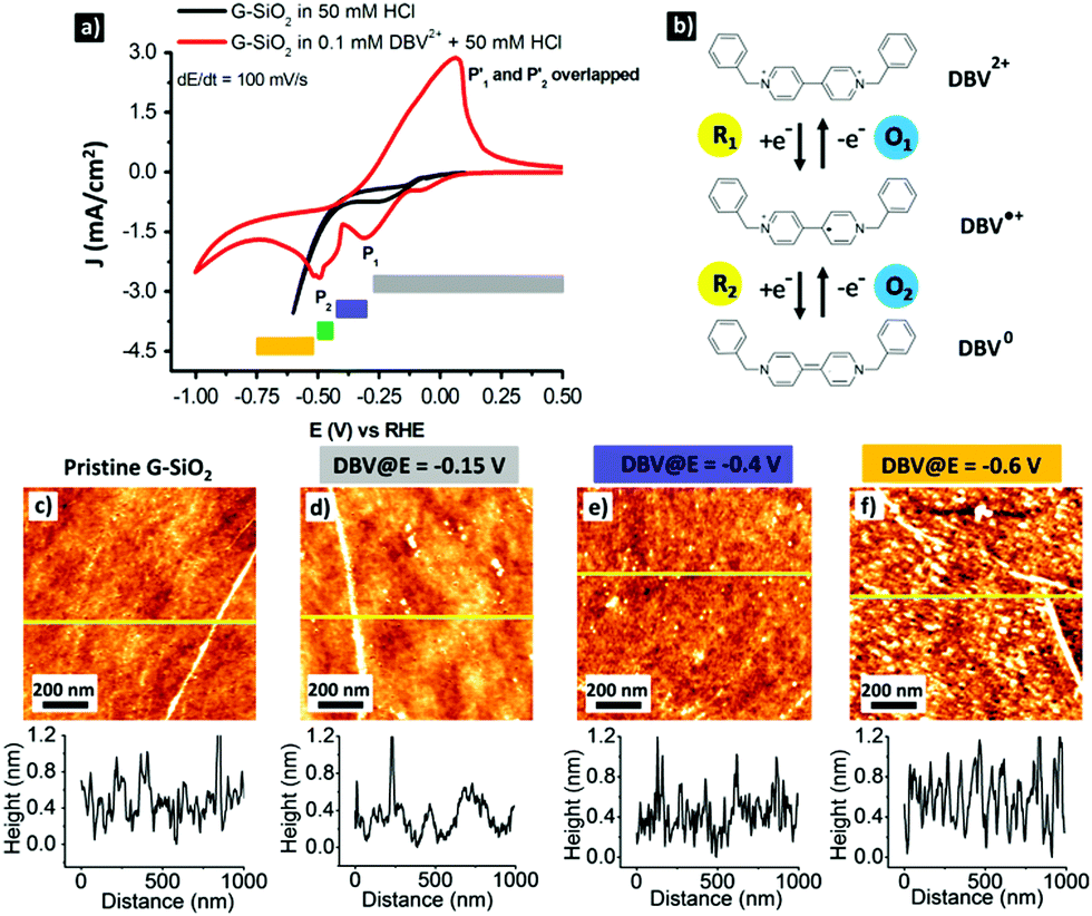 | ||
| Fig. 1 (a) CVs of G-SiO2 in 50 mM HCl (black trace) and in 0.1 mM DBV2+ + 50 mM HCl (red trace); (b) the redox states of DBV showing the transformation between dicationic, monocationic and uncharged species; AFM images and line profiles of (c) pristine G-SiO2 and (d–f) DBV-functionalized G-SiO2 prepared at different potentials. The root mean square (RMS) surface roughness of the corresponding surfaces is 0.27 nm, 0.26 nm, 0.29 nm and 0.47 nm, respectively. The RMS maximum at E = −0.6 V (f) is attributed to the deposition of the reduced DBV0 species. | ||
Based on the electrochemical behavior of G-SiO2 in DBV2+ solution, it is evident that the on-surface pattern formation by viologen on G-SiO2 will depend on the potential window. This is confirmed by AFM imaging (Fig. 1c–f). At potentials more positive than E1 = −0.3 V vs. RHE, i.e. at potentials where dicationic viologen (DBV2+) is the dominant species, rinsing with superpure water leads to pristine graphene (RMS surface roughness = 0.27 nm) which is attributed to the high solubility of DBV2+ (Fig. 1d). Between E1 = −0.3 V and E2 = −0.5 V vs. RHE, DBV2+ is electrochemically reduced to the corresponding radical mono-cationic DBV˙+ species which assembles into a so-called “dimer phase”.41,46 However, also this species is easily removed from the surface upon rinsing with water (Fig. 1e).46 The remaining topographic features (Fig. 1d and e) are attributed to water-insoluble byproducts, i.e. oligomers or polymers, formed by the radical mono-cations.46 At potentials more negative than E2 = −0.5 V, water-insoluble DBV0 is the dominant species and hence the G-SiO2 surface is fully covered by a DBV0 layer which is water-insoluble (RMS surface roughness = 0.47 nm (Fig. 1f)). At potentials more negative than E = −0.85 V, the surface is not homogeneously covered by DBV0 as disk-shaped molecule-free islands appear, likely caused by the release of hydrogen nanobubbles (see Fig. S1, ESI†).47,48
In addition to AFM, we investigated the organization of DBV0 on G-SiO2 by ambient STM (Fig. 2). Although the image resolution is inferior compared to the one obtained on graphite with EC-STM (Fig. S2, ESI†), we can conclude that also DBV0 self-assembles on G-SiO2 into the so-called stacking phase as marked by black lines in Fig. 2b, and this phase remains intact even in absence of electrochemical control. This observation demonstrates that the G-SiO2 surface is permanently functionalized by the self-assembled stacking pattern of DBV0.
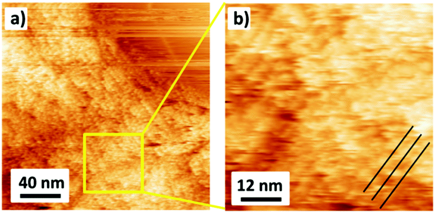 | ||
| Fig. 2 Ambient STM images show that the stacking phase of the DBV0 film remains permanently intact after being disconnected from the electrochemical cell; tunneling parameters: Vb = −0.55 V, It = 150 pA. | ||
Having established by AFM and STM that tunable patterning of the viologen species on G-SiO2 is possible we now aim to explore their doping effect with respect to graphene, a zero band gap material. The conduction band edge of graphene is at around 0 V while the reduction potentials of DBV are −0.5 V (DBV0/DBV˙+) and −0.28 V (DBV˙+/DBV2+) vs. RHE. Hence graphene may act as the electron-accepting material in presence of DBV0.49 In order to determine the degree of doping caused by DBV0 self-assembled on G-SiO2 a combination of KPFM and Raman spectroscopy was performed on pristine and DBV0 functionalized G-SiO2. Note that we refrained to use potentials more negative than E = −0.85 V vs. RHE to avoid the doping effect caused by hydrogen intercalation.50–52
KPFM, an AFM based technique, can be used to characterize the electrostatic properties of (functionalized) graphene at the nanoscale under ambient conditions by measuring the contact potential difference (CPD) between the sample surface and a conducting AFM probe.53–55 Comparison of the average (over the scanned area) values of CPD obtained for the pristine and functionalized graphene may provide relevant information on the impact of surface functionalization on doping. Mapping of the CPD distribution characterizes the degree of spatial homogeneity of the surface potential within the scanned area.
Fig. 3 shows the surface morphologies and the corresponding CPD maps obtained for pristine G-SiO2 and G-SiO2 exposed to DBV at different substrate potentials, i.e. E = −0.15 V, −0.4 V, and −0.6 V vs. RHE. Those DBV-exposed G-SiO2 samples were rinsed with MQ water and dried with Ar flow before measurement. The presented topographic images show the changes in morphology discussed above associated with electrochemical control. The corresponding KPFM measurements show some differences in the average values of CPD. Whereas the CPD measured on a micrometer scale is in general homogeneous, we see significant local variations attributed to some rare topographic features. For pristine G-SiO2 (Fig. 3a) as well as for samples prepared at E = −0.15 V (Fig. 3c) wrinkles formed during graphene growth and transfer lead to topographically higher features in the AFM image and also a corresponding higher CPD signal in the KPFM map. This contrast difference in the KPFM images is attributed to a reduced interaction with the SiO2 substrate and multilayer character of the folds (Fig. 3b, d and Fig. S3, ESI†).56
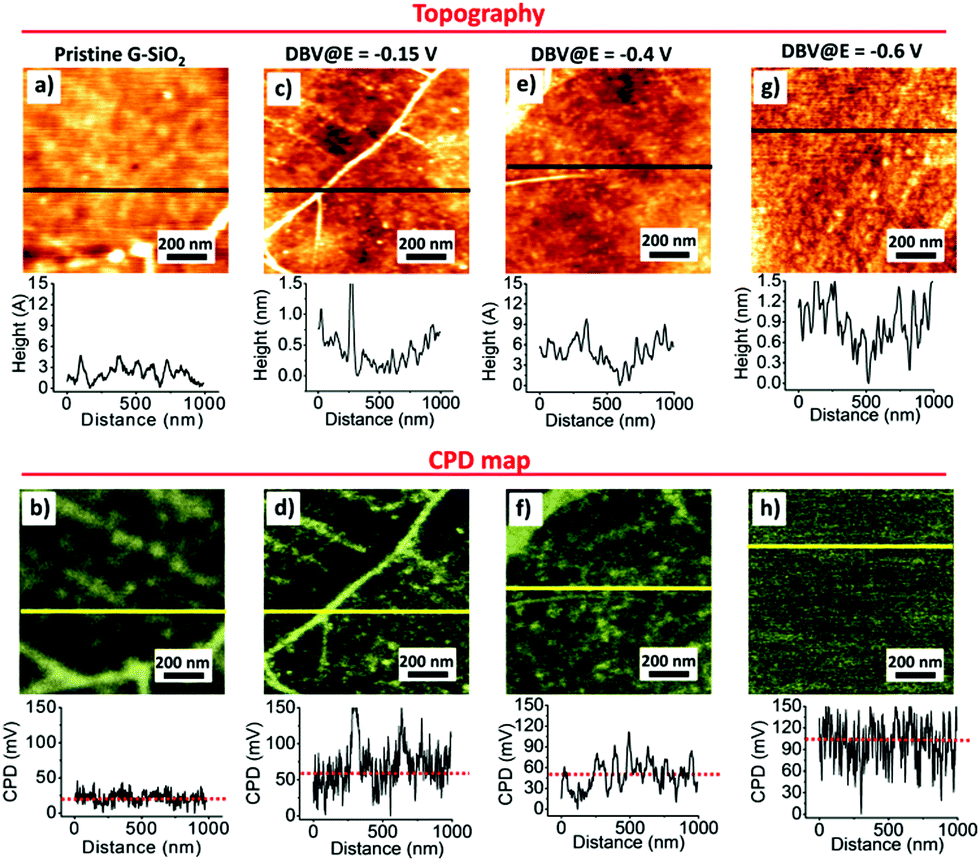 | ||
| Fig. 3 AFM topographies (a, c, e and g) and corresponding CPD mappings (b, d, f and h) of DBV functionalized G-SiO2. The electrochemical potential at which G-SiO2 is functionalized by DBV is indicated on top of the panels. | ||
The CPD signal depends on the amount and nature of DBV deposited on G-SiO2. For samples prepared at E = −0.15 V (Fig. 3c) and E = −0.4 V (Fig. 3e), G-SiO2 is either not functionalized or covered by oligomers/polymers formed by DBV˙+. Taking into account the scatter of ± 30 mV obtained form the CPD histogram (Fig. S4b, ESI†) the CPD values (Fig. 3d and f) are similar to those of pristine G-SiO2, although local variations of CPD is considerably larger. In contrast, samples prepared at E = −0.6 V where DBV0 is the dominant species (Fig. 3g and h), the surface potential is shifted by ∼95 ± 30 mV to more positive values (Fig. S4b, ESI†) relative to the surface potential value of pristine G-SiO2. At E = −0.85 V, this relative positive shift in surface potential is reduced to ∼30 mV (Fig. S5a and b, ESI†). This may be caused by a reduced surface coverage by DBV0 due hydrogen bubbling (Fig. S1a and b, ESI†). Note that an accurate quantitative estimation of the surface potential values may be affected by contaminants as well as water dipoles formed at the interface.57 However, our results show that by changing the working electrode's potential the amount of DBV0 deposited on G-SiO2 is tunable, as well as the surface potential of graphene. DBV0 has one of the lowest reduction potentials58 and hence electron transfer to graphene inducing n-doping is feasible.3,37,49
Having established by KPFM how the electrical properties of graphene change upon exposure to DBV0, the potential controlled electron donating effect was also studied by Raman spectroscopy.
Raman measurements were conducted on G-SiO2 samples before and after functionalization with DBV at selected potentials, i.e., E = −0.15 V, −0.40 V, and −0.6 V vs. RHE. Raman maps (10 × 10 μm2, 10 × 10 pixels) were recorded at 3 different locations on each sample. Based on the position shifts of the two characteristic Raman bands of graphene, i.e., the G and 2D bands, the level of doping upon functionalization can be determined. Compared to charge neutral graphene, the G band shifts to higher wave numbers upon p- and n-type doping, while the 2D band shifts to higher wave numbers for p-type doping and lower for high amounts of n-type doping. However, apart from the charge carrier concentration, also strain affects the position of both bands. To separate both effects, analysis is performed on the correlation between their positions.59 This analysis is based on the approximately linear dependence of the position of both bands on strain and p-type doping, where the 2D band position (Pos(2D)) is more sensitive to strain compared to the position of the G band (Pos(G)), while for doping the sensitivity is opposite. Consequently, in a plot of Pos(2D) versus Pos(G), the changes in doping and strain result in linear shifts of the 2D band in relation to the G band position, where the slopes of Pos(2D) verus Pos(G) are 0.7 ± 0.05 and 2.2 ± 0.2, respectively. Therefore, shifts in the peak positions in a plot of Pos(2D) and Pos(G) along a line with a slope of ≈2.2 correspond to a variation in strain, while a slope of ≈0.7 indicates doping.
Fig. 4 shows Raman spectra and plots of the 2D peak versus the G peak positions for pristine and functionalized G-SiO2. For pristine graphene, Pos(G) is around 1600 cm−1, which is at significantly higher wave numbers compared to charge neutral graphene (1581.5 cm−1). This upshift indicates that G-SiO2 is heavily p-type doped due to water and oxygen adsorbed on the surface and/or trapped between graphene and SiO2.59 To establish the impact of exposure to DBV-free electrolyte, Raman mapping was carried out on G-SiO2 exposed for 180s to the supporting electrolyte (10 mM HCl) at the polarization potential E = −0.6 V vs. RHE. After this treatment, the Raman data show a negligible difference in both the position of the G-band and 2D-band (Fig. 4a and b). Therefore, any change in the position of these peaks for G-SiO2 substrates exposed to DBV containing electrolyte can be attributed to the effect of DBV.
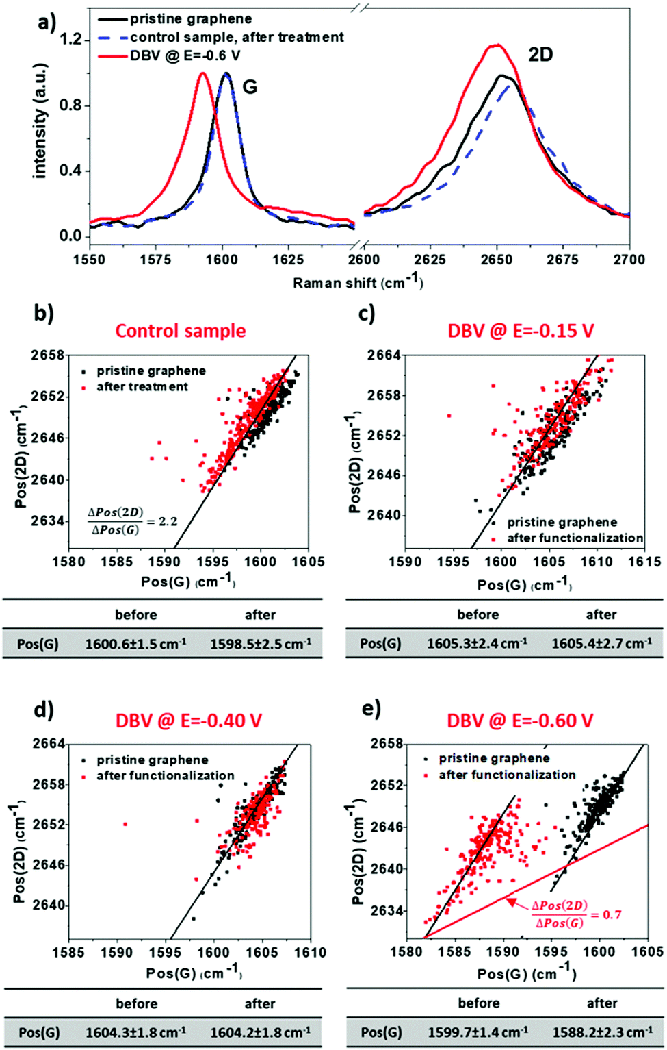 | ||
| Fig. 4 (a) Raman spectra and (b–e) plots of Pos(2D) versus Pos(G) of G-SiO2 samples before and after electrodeposition of DBV. The electrochemical potential at which G-SiO2 is functionalized by DBV is indicated on top of the panels. The black lines in (b–e) have a slope of 2.2 and highlight the variation in strain and the red guideline in (e) indicates the direction in shift of the data points upon doping. | ||
Fig. 4c illustrates the plots of Pos(2D) versus Pos(G) of G-SiO2 before and after exposure to DBV containing electrolyte. Note that for all measurements, the spread of the data points follows a line with a slope of approximately 2.2, which is caused by strain variations in graphene.60 No shift was detected for samples polarized at E = −0.15 V and E = −0.4 V, respectively (Fig. 4c and d). However, a significant red shift in Pos(G) (11.5 ± 1.5 cm−1), was observed with samples polarized at E = −0.6 V (Fig. 4a and e). This shift indicates a reduction in p-type doping and therefore a net n-type doping effect after functionalization. In addition to a shift of Pos(G), the n-type doping is corroborated by an increase of the intensity ratio of the 2D versus the G band and an increase of the full width at half maximum of the G band (Table S1, ESI†) after functionalization. Using experimental data in ref. 61, the number of electrons injected into graphene can be estimated to be approximately 8 × 1012 cm−2.61 The results are attributed to the homogeneous coverage of DBV0 on G-SiO2. Furthermore, no significant increase in D band intensity was observed after functionalization with DBV, demonstrating that the electrodeposition process does not induce defects in graphene (Fig. S6 and Table S1, ESI†). A smaller red shift in Pos(G) (7.8 ± 1.2 cm−1) for the sample prepared at E = −0.85 V (Fig. S5c, ESI†), is attributed to a reduced DBV0 coverage due to hydrogen evolution reaction at this potential.
In combination with the positive shift of the surface potential as revealed by KPFM, the red shift of the G peak supports an n-type doping effect caused by adsorbed DBV0 molecules. It is worth emphasizing that in comparison with other methods employed to dope graphene by viologens3,37,49 our approach has the advantage of easy control of the doping level due to its one-step protocol and redox state controlled self-assembly process in a compact environment.
Conclusions
We have demonstrated a one-step process to form a self-assembled adlayer of DBV0 that can be used as n-type dopant for CVD graphene. Upon controlling the electrochemical potential, conditions are generated where exclusively DBV0 molecules are deposited in a self-assembled manner on G-SiO2. The film morphology and n-type doping effect of DBV0 was elucidated using a combination of STM, AFM, KPFM and Raman spectroscopy. This non-destructive bottom-up strategy opens up a new avenue to dope graphene by organic self-assembled adlayers using redox-active molecules under electrochemical control.Author contributions
H. T. M. T. and T. H. P. prepared the samples. H. T. M. T. conducted and analyzed the CV, STM and EC-STM data. T. H. P. recorded and analyzed the AFM data. R. P. performed and analyzed the Raman data. A. V. performed KPFM measurements. T. M. T. H. and S. D. F. conceived and designed the work. T. H. P., T. M. T. H., and S. D. F. cowrote the paper. All authors contributed to the discussion of the results and commented on the manuscript.Conflicts of interest
The authors declare no competing financial interest.Acknowledgements
This research is funded by Vietnam National Foundation for Science and Technology Development (Nafosted) under grant number 104.05-2019.52. S. D. F. gratefully acknowledges financial support from the Fund of Scientific Research Flanders (FWO), KU Leuven – Internal Funds (C14/19/079) and EOS 30489208.Notes and references
- A. K. Geim, Science, 2009, 324, 1530 CrossRef.
- K. S. Novoselov, A. K. Geim, S. V. Morozov, D. Jiang, Y. Zhang, S. V. Dubonos, I. V. Grigorieva and A. A. Firsov, Science, 2004, 306, 666–669 CrossRef PubMed.
- H. K. Jeong, K.-j. Kim, S. M. Kim and Y. H. Lee, Chem. Phys. Lett., 2010, 498, 168–171 CrossRef.
- X. Chen, X. Duan, W.-D. Oh, P.-H. Zhang, C.-T. Guan, Y.-A. Zhu and T.-T. Lim, Appl. Catal., B, 2019, 253, 419–432 CrossRef.
- P. Joshi, H.-H. Huang, R. Yadav, M. Hara and M. Yoshimura, Catal. Sci. Technol., 2020, 10, 6599–6610 RSC.
- R. Pawlak, X. Liu, S. Ninova, P. D’Astolfo, C. Drechsel, S. Sangtarash, R. Häner, S. Decurtins, H. Sadeghi, C. J. Lambert, U. Aschauer, S.-X. Liu and E. Meyer, J. Am. Chem. Soc., 2020, 142, 12568–12573 CrossRef.
- H. Xu, L. Ma and Z. Jin, J. Energy Chem., 2018, 27, 146–160 CrossRef.
- M. Z. Hossain, M. A. Walsh and M. C. Hersam, J. Am. Chem. Soc., 2010, 132, 15399–15403 CrossRef PubMed.
- Z. Qiu, J. Yu, P. Yan, Z. Wang, Q. Wan and N. Yang, ACS Appl. Mater. Interfaces, 2016, 8, 28291–28298 CrossRef PubMed.
- Z. Xia, F. Leonardi, M. Gobbi, Y. Liu, V. Bellani, A. Liscio, A. Kovtun, R. Li, X. Feng, E. Orgiu, P. Samorì, E. Treossi and V. Palermo, ACS Nano, 2016, 10, 7125–7134 CrossRef.
- J. Greenwood, T. H. Phan, Y. Fujita, Z. Li, O. Ivasenko, W. Vanderlinden, H. Van Gorp, W. Frederickx, G. Lu, K. Tahara, Y. Tobe, H. Uji-i, S. F. L. Mertens and S. De Feyter, ACS Nano, 2015, 9, 5520–5535 CrossRef.
- T. H. Phan, H. Van Gorp, Z. Li, T. M. Trung Huynh, Y. Fujita, L. Verstraete, S. Eyley, W. Thielemans, H. Uji-i, B. E. Hirsch, S. F. L. Mertens, J. Greenwood, O. Ivasenko and S. De Feyter, ACS Nano, 2019, 13, 5559–5571 CrossRef PubMed.
- K. Fan, X. Liu, Y. Liu, Y. Li, Y. Chen, Y. Meng, X. Liu, W. Feng and L. Luo, Carbon, 2020, 167, 826–834 CrossRef.
- C. Meng, Q. Chen, X. Li and H. Liu, J. Membr. Sci., 2019, 582, 83–90 CrossRef.
- K. R. Nandanapalli, D. Mudusu and S. Lee, Carbon, 2019, 152, 954–985 CrossRef.
- G. Ambrosio, A. Brown, L. Daukiya, G. Drera, G. Di Santo, L. Petaccia, S. De Feyter, L. Sangaletti and S. Pagliara, Nanoscale, 2020, 12, 9032–9037 RSC.
- H. Wang, T. Maiyalagan and X. Wang, ACS Catal., 2012, 2, 781–794 CrossRef.
- B. Cai, S. Zhang, Z. Yan and H. Zeng, ChemNanoMat, 2015, 1, 542–557 CrossRef.
- T. Torres, Chem. Soc. Rev., 2017, 46, 4385–4386 RSC.
- A. Lopez and J. Liu, Adv. Intell. Syst., 2020, 2, 2000123 CrossRef.
- M. Gobbi, S. Bonacchi, J. X. Lian, Y. Liu, X.-Y. Wang, M.-A. Stoeckel, M. A. Squillaci, G. D’Avino, A. Narita, K. Müllen, X. Feng, Y. Olivier, D. Beljonne, P. Samorì and E. Orgiu, Nat. Commun., 2017, 8, 14767 CrossRef.
- A. Ciesielski and P. Samorì, Adv. Mater., 2016, 28, 6030–6051 CrossRef PubMed.
- K. S. Mali, J. Greenwood, J. Adisoejoso, R. Phillipson and S. De Feyter, Nanoscale, 2015, 7, 1566–1585 RSC.
- K. Madasamy, D. Velayutham, V. Suryanarayanan, M. Kathiresan and K.-C. Ho, J. Mater. Chem. C, 2019, 7, 4622–4637 RSC.
- G. Huseynova, N. K. Shrestha, Y. Xu, E.-Y. Shin, W.-T. Park, D. Ji and Y.-Y. Noh, Org. Electron., 2018, 62, 572–580 CrossRef.
- K. W. Shah, S.-X. Wang, D. X. Y. Soo and J. Xu, Polymers, 2019, 11, 1839 CrossRef CAS.
- Z. Mi, T. Zhou, W. Weng, J. Unruangsri, K. Hu, W. Yang, C. Wang, K. A. I. Zhang and J. Guo, Angew. Chem., Int. Ed., 2021, 60, 9642–9649 CrossRef CAS.
- B. A. MacLeod, N. J. Stanton, I. E. Gould, D. Wesenberg, R. Ihly, Z. R. Owczarczyk, K. E. Hurst, C. S. Fewox, C. N. Folmar, K. Holman Hughes, B. L. Zink, J. L. Blackburn and A. J. Ferguson, Energy Environ. Sci., 2017, 10, 2168–2179 RSC.
- S. Y. Lee, S. W. Lee, S. M. Kim, W. J. Yu, Y. W. Jo and Y. H. Lee, ACS Nano, 2011, 5, 2369–2375 CrossRef CAS.
- W. J. Yu, L. Liao, S. H. Chae, Y. H. Lee and X. Duan, Nano Lett., 2011, 11, 4759–4763 CrossRef CAS.
- V. Rebuttini, E. Fazio, S. Santangelo, F. Neri, G. Caputo, C. Martin, T. Brousse, F. Favier and N. Pinna, Chem. – Eur. J., 2015, 21, 12465–12474 CrossRef CAS.
- H. Ren, Y. Zhou, Y. Wang, X. Zhu, C. Gao and Y. Guo, Sens. Actuators, B, 2020, 321, 128520 CrossRef CAS.
- K. Matsuyama, A. Fukui, K. Miura, H. Ichimiya, Y. Aoki, Y. Yamada, A. Ashida, T. Yoshimura, N. Fujimura and D. Kiriya, ChemistryOpen, 2019, 8, 908–914 CrossRef CAS PubMed.
- K. Jo, J. Choi and H. Kim, J. Mater. Chem. C, 2017, 5, 5395–5401 RSC.
- B. Chamlagain, S. S. Withanage, A. C. Johnston and S. I. Khondaker, Sci. Rep., 2020, 10, 12970 CrossRef CAS PubMed.
- S. Kim, C. Kim, Y. H. Hwang, S. Lee, M. Choi and B.-K. Ju, Chem. Phys. Lett., 2021, 770, 138453 CrossRef CAS.
- S. Y. Lee, D. L. Duong, Q. A. Vu, Y. Jin, P. Kim and Y. H. Lee, ACS Nano, 2015, 9, 9034–9042 CrossRef CAS PubMed.
- M. Wilms, M. Kruft, G. Bermes and K. Wandelt, Rev. Sci. Instrum., 1999, 70, 3641–3650 CrossRef CAS.
- I. Horcas, R. Fernández, J. M. Gómez-Rodríguez, J. Colchero, J. Gómez-Herrero and A. M. Baro, Rev. Sci. Instrum., 2007, 78, 013705 CrossRef CAS.
- R. Phillipson, C. J. Lockhart de la Rosa, J. Teyssandier, P. Walke, D. Waghray, Y. Fujita, J. Adisoejoso, K. S. Mali, I. Asselberghs, C. Huyghebaert, H. Uji-i, S. De Gendt and S. De Feyter, Nanoscale, 2016, 8, 20017–20026 RSC.
- T. M. T. Huynh, T. H. Phan, O. Ivasenko, S. F. L. Mertens and S. De Feyter, Nanoscale, 2017, 9, 362–368 RSC.
- T. H. Phan and K. Wandelt, Beilstein J. Org. Chem., 2014, 10, 2243–2254 CrossRef.
- D.-T. Pham, K. Gentz, C. Zörlein, N. T. M. Hai, S.-L. Tsay, B. Kirchner, S. Kossmann, K. Wandelt and P. Broekmann, New J. Chem., 2006, 30, 1439–1451 RSC.
- C. L. Bird and A. T. Kuhn, Chem. Soc. Rev., 1981, 10, 49–82 RSC.
- D.-T. Pham, S.-L. Tsay, K. Gentz, C. Zoerlein, S. Kossmann, J.-S. Tsay, B. Kirchner, K. Wandelt and P. Broekmann, J. Phys. Chem. C, 2007, 111, 16428–16436 CrossRef CAS.
- S. Breuer, D. T. Pham, S. Huemann, K. Gentz, C. Zoerlein, R. Hunger, K. Wandelt and P. Broekmann, New J. Phys., 2008, 10, 125033 CrossRef.
- L. Zhang, Y. Zhang, X. Zhang, Z. Li, G. Shen, M. Ye, C. Fan, H. Fang and J. Hu, Langmuir, 2006, 22, 8109–8113 CrossRef CAS.
- F. Hui, B. Li, P. He, J. Hu and Y. Fang, Electrochem. Commun., 2009, 11, 639–642 CrossRef CAS.
- D. Kiriya, M. Tosun, P. Zhao, J. S. Kang and A. Javey, J. Am. Chem. Soc., 2014, 136, 7853–7856 CrossRef CAS PubMed.
- I. Takuya, S. Jian, K. Nozomu, C. Takuo, A. Masashi, M. Manoharan and M. Hiroshi, Appl. Phys. Express, 2015, 8, 015101 CrossRef.
- S. Y. Davydov, Semiconductors, 2017, 51, 640–644 CrossRef CAS.
- J. Grzonka, I. Pasternak, P. P. Michałowski, V. Kolkovsky and W. Strupinski, Appl. Surf. Sci., 2018, 447, 582–586 CrossRef CAS.
- X. Zhou, S. He, K. A. Brown, J. Mendez-Arroyo, F. Boey and C. A. Mirkin, Nano Lett., 2013, 13, 1616–1621 CrossRef CAS.
- C. Barth, A. S. Foster, C. R. Henry and A. L. Shluger, Adv. Mater., 2011, 23, 477–501 CrossRef CAS.
- Y. Shi, K. K. Kim, A. Reina, M. Hofmann, L.-J. Li and J. Kong, ACS Nano, 2010, 4, 2689–2694 CrossRef CAS PubMed.
- F. Long, P. Yasaei, R. Sanoj, W. Yao, P. Král, A. Salehi-Khojin and R. Shahbazian-Yassar, ACS Appl. Mater. Interfaces, 2016, 8, 18360–18366 CrossRef CAS.
- M. C. R. González, P. Carro, L. Vázquez and A. H. Creus, Phys. Chem. Chem. Phys., 2016, 18, 29218–29225 RSC.
- S. M. Kim, J. H. Jang, K. K. Kim, H. K. Park, J. J. Bae, W. J. Yu, I. H. Lee, G. Kim, D. D. Loc, U. J. Kim, E.-H. Lee, H.-J. Shin, J.-Y. Choi and Y. H. Lee, J. Am. Chem. Soc., 2009, 131, 327–331 CrossRef CAS.
- S. Ryu, L. Liu, S. Berciaud, Y.-J. Yu, H. Liu, P. Kim, G. W. Flynn and L. E. Brus, Nano Lett., 2010, 10, 4944–4951 CrossRef CAS.
- C. Neumann, S. Reichardt, P. Venezuela, M. Drögeler, L. Banszerus, M. Schmitz, K. Watanabe, T. Taniguchi, F. Mauri, B. Beschoten, S. V. Rotkin and C. Stampfer, Nat. Commun., 2015, 6, 8429 CrossRef CAS PubMed.
- M. Bruna, A. K. Ott, M. Ijäs, D. Yoon, U. Sassi and A. C. Ferrari, ACS Nano, 2014, 8, 7432–7441 CrossRef CAS.
Footnotes |
| † Electronic supplementary information (ESI) available. See DOI: 10.1039/d1tc03142b |
| ‡ These authors contributed equally to this work. |
| This journal is © The Royal Society of Chemistry 2022 |