
Quasi-2D halide perovskite crystals and their optoelectronic applications
Xin
Sheng
ab,
Yahui
Li
b,
Ming
Xia
b and
Enzheng
Shi
 *b
*b
aSchool of Materials Science & Engineering, Zhejiang University, Hangzhou, 310027, China
bSchool of Engineering, Westlake University, Hangzhou, 310024, China. E-mail: shienzheng@westlake.edu.cn
First published on 10th May 2022
Abstract
Due to the widely tunable and exceptional semiconductor properties, quasi-two-dimensional (2D) halide perovskites have been considered outstanding candidates for next-generation optoelectronic devices and have thus undergone rapid development over the last decade. Their property tunability is intimately correlated with the quantum-well thickness (corresponding to the n value, the number of octahedral layers in each layer of quasi-2D halide perovskites). However, a systematic review of the relationship between the n value and the optoelectronic properties/applications of the quasi-2D perovskites is lacking. In this review, we begin with the n-dependent properties of quasi-2D perovskites, and move on to the synthesis of different forms of quasi-2D perovskite crystals. Afterwards, we focus on the existing optoelectronic applications using quasi-2D perovskites including light-emitting diodes, solar cells, lasers, and photodetectors. In the last section, we discuss the current challenges and a few promising directions with a special focus on the precise control of the n value. Moreover, the possible non-centrosymmetrical ordering of the organic ligands in quasi-2D halide perovskites provides new insights and opportunities to study the interaction between spontaneous polarization, photovoltaic effect, and carrier transport behaviors in the corresponding electronic and optoelectronic devices.
 Enzheng Shi | Enzheng Shi is currently an assistant professor at the School of Engineering, Westlake University. Dr Shi received his bachelor's degree from Shandong University in 2010 and PhD degree from Peking University in 2015. He worked as a postdoc research associate in Iowa State University from 2015 to 2017, and in Purdue University from 2017 to 2020, respectively. His research interests cover two aspects: (1) design, synthesis, and applications of novel electronic materials and heterostructures; and (2) assembly and manipulation of low-dimensional carbon nanomaterials. |
1. Introduction
The last decade has witnessed the explosive development of layered halide perovskites in high-performance optoelectronic devices (solar cells,1–5 light-emitting diodes,6–10 lasers,11–15 photodetectors,16–20etc.) due to their marvelous optoelectronic properties and high stability.Layered halide perovskites consist of metal halide octahedra sandwiched by symmetrical layers of organic ligands. According to the variation in organic ligands, they can be generally classified into three types:21–25 Ruddlesden–Popper (RP) phase,26 Dion–Jacobson (DJ) phase27,28 and alternating cations in the interlayer space (ACI) phase.29 The common expression of the RP phase is L2An−1MnX3n+1, where L stands for large organic ammonium cations, A for small cations (e.g., Cs+, CH3NH3+ (MA+) and CH3(NH2)2+ (FA+)), M for divalent metals like Pb2+, and X for halogen anions (I−, Br− and Cl−). In addition, the number of octahedral layers in each layer of 2D halide perovskites is specified by another unique parameter, n. 2D perovskites with n = 1 and n > 1 (high n) can also be designated as pure-2D and quasi-2D perovskites, respectively.
The major distinction between RP phase, DJ phase and ACI phase perovskites originates from the large organic ligand L (Fig. 1a). In the RP phase, monoammonium cations are used as large organic ligands and the adjacent layers are connected by van der Waals force. The molecular structure of several reported ligands is listed in Fig. 1b. In the DJ phase, however, diammonium cations are applied to chemically link adjacent layers together, making mechanical exfoliation of DJ phase perovskites into molecularly thin sheets impossible. ACI phase halide perovskites are considered to combine the RP phase's chemical formula and the DJ phase's structural properties.30 Despite the fact that the ACI phase is supposed to have better performance, a complete grasp of its intrinsic properties remains unclear due to the lack of investigation into single crystals. Due to the ease of mechanical exfoliation into thin sheets, molecularly flat surface and no dangling bonds at the surface, RP phase perovskites are the most well-investigated among the three types of layered perovskites mentioned above and thus will be mainly discussed in this review.
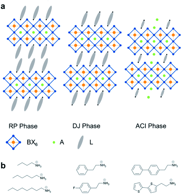 | ||
| Fig. 1 Structure of 2D halide perovskites. (a) Schematic representation of Ruddlesden–Popper (RP) phase, Dion–Jacobson (DJ) phase and alternating cations in the interlayer space (ACI) phase 2D perovskites. (b) Some ligands employed in RP phase 2D perovskites. | ||
One merit of 2D halide perovskites is their wide property tunability resulting from facile and flexible composition engineering.31–36 They can be substituted completely or partially by other similar ions. Additionally, adjusting the n value has a significant impact on their optoelectronic properties. Reports indicate that quasi-2D perovskites combine the enhanced stability of pure-2D perovskites with the superior carrier mobility of their 3D counterparts, and optoelectronic devices based on quasi-2D perovskites outperform those based on pure-2D perovskites.37 Though quasi-2D perovskites show attractive properties and promising applications, their systematic summary is rarely seen.
In this review, we'll focus on the properties, synthesis and applications of RP phase quasi-2D perovskites (n > 1). We begin with emphasizing the dependence of semiconductor properties on the n value. Then the synthesis methodologies of quasi-2D perovskites in various crystal forms are summarized. The next section covers optoelectronic applications, such as light-emitting diodes, solar cells, lasers, and photodetectors. Finally, we summarize the current challenges and outlook of the quasi-2D perovskites.
2. Properties
2.1 Quantum and dielectric confinement
2D halide perovskites could be considered as quantum wells formed by sandwiching octahedral layers by organic ligand layers in the out-of-plane direction.38–40 Typically, the band gap of the insulating organic ligand layer is substantially larger than that of the octahedral layer, thus forming type-I band alignment. As a result, the excited electrons and holes will be confined in the octahedral layer. Quantum confinement and dielectric screening effects have a huge impact on the charge carrier behaviours of 2D perovskites,41–44 which is directly correlated with the thickness of the quantum wells (n value). As n increases, the coupling effect between the electrons and holes weakens, leading to an increase in exciton transport distance and drop in exciton density and binding energy45 (Fig. 2a).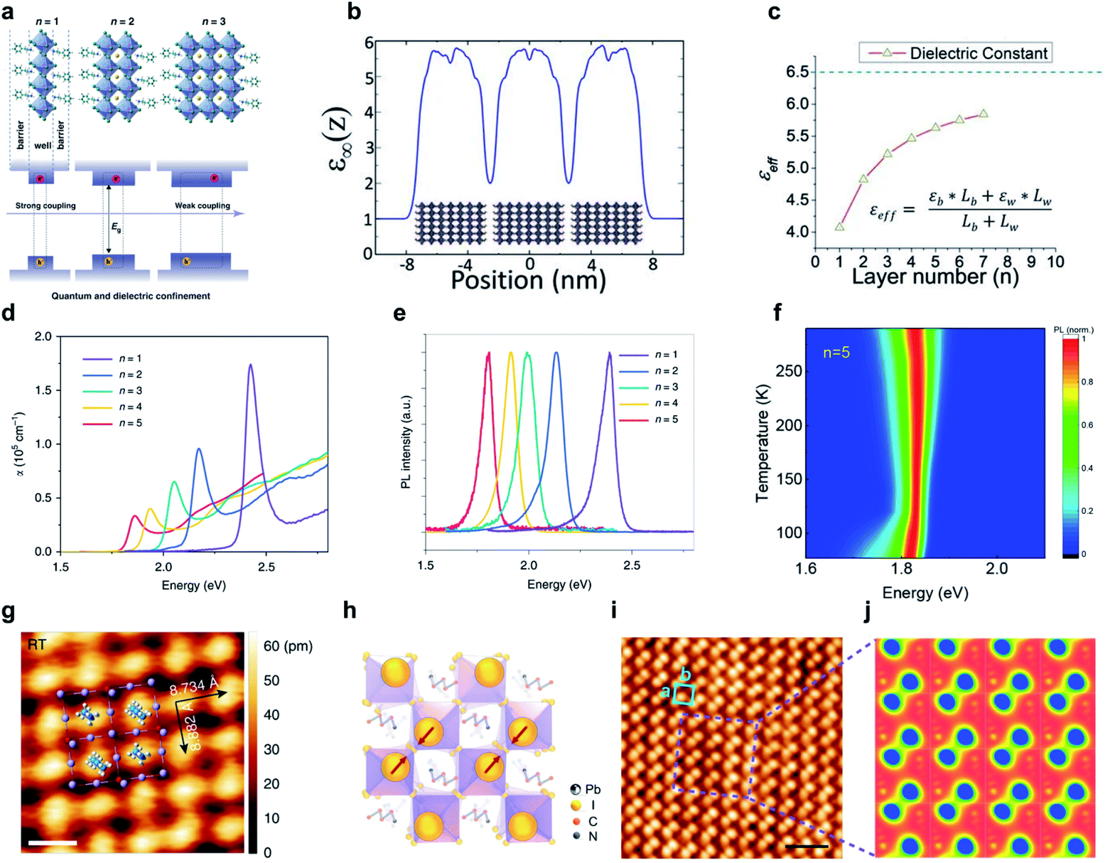 | ||
| Fig. 2 Quantum-well structure of RP phase perovskites and their optical properties as well as surface morphology. (a) Quantum-well structure of layered perovskites45 (Copyright: 2021, Light: Science & Applications). (b) Calculated high-frequency dielectric constant of (BA)2(MA)5Pb7I22 in the stacking direction46 (Copyright: 2019, Proceedings of the National Academy of Sciences of the United States of America). (c) Relationship between the effective high-frequency dielectric constant and n value46 (Copyright: 2019, Proceedings of the National Academy of Sciences of the United States of America). (d) Absorption and (e) PL spectra of BA2MAn−1PbnI3n+1 (n = 1–5)48 (Copyright: 2020, Nature Communications); (f) temperature dependent PL of (BA)2MA4Pb5I16 (ref. 51) (Copyright: 2019, The Journal of Physical Chemistry Letters). (g) Q-Plus non-contact AFM image at room temperature of (BA)2MA3Pb4I13 (scale bar: 1 nm)17 (Copyright: 2018, Nature Materials). (h) Schematic surface structure after relaxation.53 (i) Atomic-resolution STM image of (BA)2MA3Pb4I13 (scale bar: 2 nm) and (j) relative simulated charge density plot53 (Copyright: 2022, Nature Communications). | ||
In 2D halide perovskites, effective high-frequency dielectric coefficients will increase as n increases. Taking the BA2MAn−1PbnI3n+1 (n = 1–7) series for example, the computed high-frequency dielectric constant (ε∞) along the out-of-plane direction is around 5.8 for octahedral layers and around 2.0 for organic layers46 (Fig. 2b). With the increase of the n value, the contribution of octahedral layers to the effective high-frequency dielectric coefficient increases, resulting in a rise in the effective high-frequency dielectric coefficient46 (Fig. 2c). Fig. 2c also shows the mathematical expression for this regulation, where εb is the high-frequency dielectric constant of the organic layer component, Lb is the length of the organic layer component, εw is the high-frequency dielectric constant of the inorganic layer component, and Lw is the length of the inorganic layer component.
2.2 Optical properties
The n-dependent optical properties can be characterized roughly by absorption spectroscopy and photoluminescence (PL) spectroscopy. For 2D perovskites with strong exciton absorption, the Tauc plot method is commonly used to extract the corresponding optical band gap from UV-vis absorption spectra.47 Due to the quantum confinement and dielectric screening effects, the band gap of quasi-2D halide perovskites will decrease with n value. The optical band gap of (BA)2PbI4 is 2.42 eV, as shown in Fig. 2d, and drops to 1.85 eV for (BA)2MA4Pb5I16.48Consistent with the UV-vis spectra, the PL emission peaks of 2D perovskites also change with n value (Fig. 2e).48 In the BA2MAn−1PbnI3n+1 series, the PL emission redshifts from green (∼520 nm for (BA)2PbI4) to red (680 nm for (BA)2MA4Pb5I16) as the n value increases from 1 to 4. In addition, the PL peaks of n = 6 and n = 7 could further red-shift to around 700 nm and 713 nm, respectively.46 Because of the self-absorption in bulk crystals, the PL intensity of monolayers is frequently stronger than that of the bulk for a quasi-2D perovskite with a given n value.17
The PL efficiency of 2D perovskites relies on several factors, one of which is electron–phonon coupling. As the lattice of 2D perovskites is quite soft, the interaction of phonons and electrons is more pronounced.49 The PL efficiency will be significantly affected by the strength and mechanism of electron–phonon coupling,50 which can be obtained by analysing temperature-dependent PL spectra51 (Fig. 2f). As revealed by the density functional theory (DFT) calculation, the rigidity of the organic ligands also plays an important role in the electron–phonon interaction. With enhanced rigidity of the organic ligands in 2D halide perovskites, the structure fluctuation of the perovskite will be suppressed, resulting in reduced exciton–phonon coupling and increased PL efficiency.52
2.3 Surface state
The material surface generally possesses distinct properties compared with the bulk regions. To study the surface states without the effect from the bulk states, Leng et al.17 employed monolayer crystals obtained by mechanical exfoliation. The surface of the exfoliated perovskite (BA)2MA3Pb4I13 is initially a well-ordered periodic square lattice with minimal density of holes and defects, according to the high-resolution atomic force microscopy (AFM) characterization17 (Fig. 2g). Upon heating, the organic cation at the surface will reorient, which will have a direct impact on the PL emission. This impact weakens with the increase of the n value.Apart from high-resolution AFM, scanning tunnelling microscopy (STM) is another tool to directly visualize the surface states. Shao et al.53 proposed a model based on monolayer (BA)2MA3Pb4I13 perovskites, suggesting that the stronger out-of-plane tilt of adjacent Pb–I octahedra toward each other will naturally push their apical I atoms closer, forming a “dimer-like” structure eventually (Fig. 2h). The obtained STM image of (BA)2MA3Pb4I13 (Fig. 2i) demonstrated a clear dimer structure corresponding to the iodine atom at the top, which is further verified by the simulated charge density image53 (Fig. 2j).
2.4 Transport behaviours
With strongly bound excitons and tunable band structures, quasi-2D perovskites are ideal candidates for optoelectronic applications, where exciton transport and annihilation are two key processes. Deng et al.48 employed transient absorption microscopy to quantify the n-dependent exciton diffusion and annihilation in perovskites with different n values, revealing the key role of electron–hole interaction and dielectric screening. For BA2MAn−1PbnI3n+1, the exciton diffusion constant increases as the quantum well becomes thicker, ranging from 0.06 to 0.34 cm2 s−1, resulting in exciton diffusion in the hundreds of nanometre range48 (Fig. 3a). With increasing n value, the rate of exciton annihilation decreases48 (Fig. 3b). The combination of long exciton transport distance and slow annihilation rate highlights the unique properties of 2D perovskites as exciton-like optoelectronic materials. In addition, the exciton annihilation rate in 2D halide perovskites is orders of magnitude lower than that of monolayer transition metal dichalcogenides.54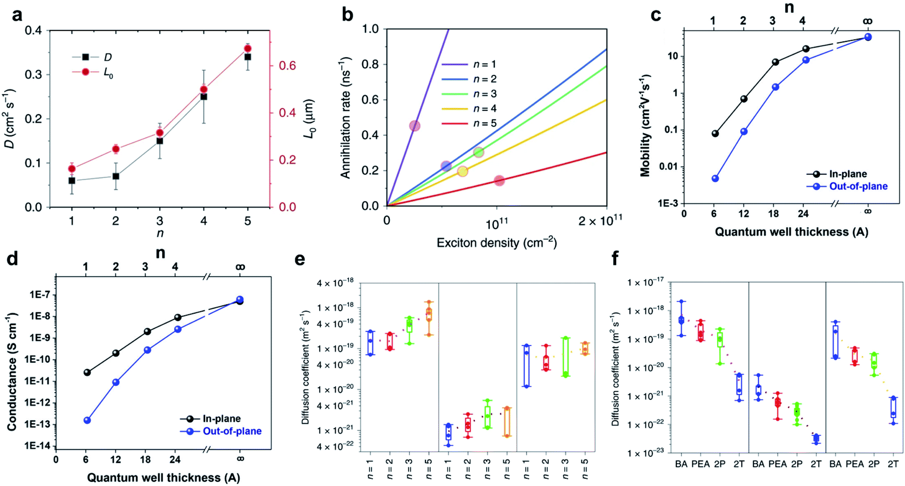 | ||
| Fig. 3 Carrier behaviour in 2D perovskites. (a) Diffusion constant, (b) annihilation rate48 (Copyright: 2020, Nature Communications), (c) mobility and (d) conductance55 (Copyright: 2018, ACS Nano) as a function of n value in the (BA)2MAn−1PbnI3n+1 series. Comparison of the impact of (e) the n value and (f) ligands on the halogen diffusion constant. Left, Fickian diffusion coefficients; middle, non-Fickian diffusion coefficients; right, diffusion coefficients by KMC simulation56 (Copyright: 2021, Nature Nanotechnology). | ||
Due to the layered structure, the electronic properties of quasi-2D halide perovskites are anisotropic. Using the space charge current limiting approach, Wang et al.55 investigated the in-plane and out-of-plane charge transport properties of BA2MAn−1PbnI3n+1. The in-plane properties were studied by vapor-plating two electrodes on one side while the out-of-plane properties were studied by vapor-plating two electrodes on opposite sides. Both the carrier mobility and electrical conductivity increase in both in-plane and out-of-plane directions as the n value increases. Because of the organic barriers and van der Waals interaction along the out-of-plane direction, the in-plane carrier mobility and electrical conductivity are always higher than those along the out-of-plane direction (Fig. 3c and d). However, the discrepancies between these properties along the two directions decrease as the n value increases, indicating the reduced anisotropy for high-n quasi-2D halide perovskites.55
In addition to the motion of charge carriers, the organic ligands and n value in the 2D halide perovskites also have a significant impact on the ion motion within the soft lattice. For instance, by assembling vertical heterostructures between different 2D halide perovskites, Akriti et al.56,57 investigated the influence of the n value and ligands on anionic diffusion. The vertical heterostructures are made up of a top iodide perovskite and bottom bromide perovskite. Upon varying the n value of the top BA2MAn−1PbnI3n+1 from 1 to 5, the anionic diffusion coefficient increases gradually according to three different independent diffusion models, suggesting faster halide migration in higher n perovskites (Fig. 3e). When it comes to the effect of organic cations, it was discovered that bulkier π-conjugated ligands like bithiophenylethylammonium (2T) are more effective in preventing halide diffusion than benzene-based π-conjugated systems or short-chain aliphatic ligands, implying that molecular engineering and dimensional engineering could be helpful to effectively suppress anionic diffusion (Fig. 3f).
3. Synthetic strategies
Quasi-2D perovskites can be synthesized in different forms. In this section, we will summarize the synthesis methodologies for quasi-2D perovskite single crystals, nanosheets and thin films, and discuss the existing challenges in crystal synthesis.3.1 Bulk single crystals
Quasi-2D halide perovskite single crystals are essential to determine their crystal structure and investigate their intrinsic properties due to their low density of defects and impurities. To synthesize phase-pure quasi-2D halide perovskite single crystals with precise control of the n value, a deep understanding of 2D halide perovskite single crystals as well as their growth mechanism is of great significance.To grow quasi-2D halide perovskite single crystals, various techniques have been developed. The slow-cooling method (Fig. 4a) is one of the widely utilized strategies, in which the precursors are first added to the solvent (typically mixed acids containing hydroiodic/hydrobromic acid and hypophosphorous acid). After that, the solution will be heated to dissolve the precursors until it becomes clear. In the process of cooling, the supersaturation of the halide perovskites in the solution causes the nucleation of the desired phase. The final quasi-2D halide perovskite bulk crystals will be collected until the solution reaches room temperature. Using this method, BA2MAn−1PbnI3n+1 (n = 1–4)58 were synthesized with centimeter size, followed by the n = 5 (ref. 59), 6 and 7 (ref. 46 and 60) counterparts (Fig. 4b).
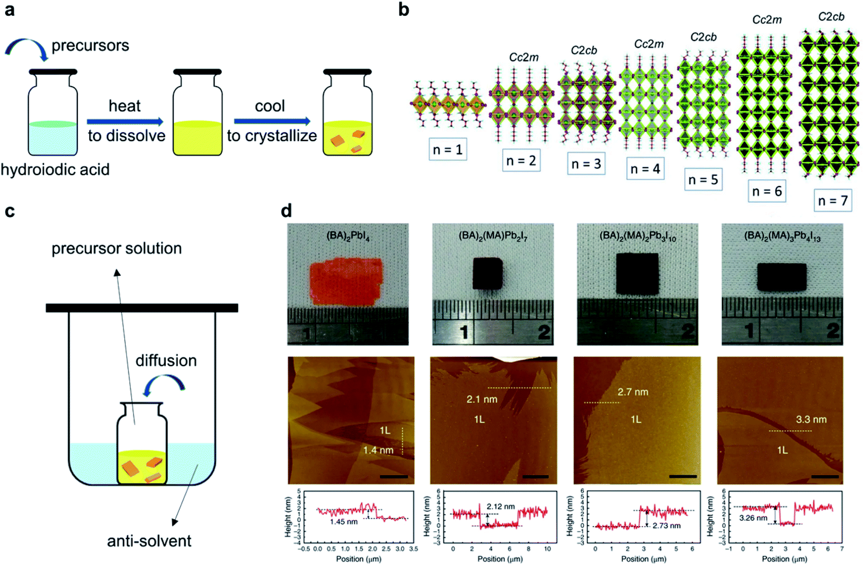 | ||
| Fig. 4 Growing methods of bulk single crystals. (a) Schematics of the slow-cooling method. (b) Crystal structure of BA2MAn−1PbnI3n+1 (n = 1–7)46 (Copyright: 2019, Proceedings of the National Academy of Sciences of the United States of America). (c) Schematics of the anti-solvent diffusion method. (d) Optical images of BA2PbI4, BA2MAPb2I7, BA2MA2Pb3I10 and BA2MA3Pb4I13 bulk crystals and corresponding AFM images (scale bars: 4 μm)17 (Copyright: 2018, Nature Materials). | ||
Additional methods for synthesis of quasi-2D halide perovskite bulk crystals include anti-solvent diffusion,68 slow evaporation,63,77 temperature-gradient-controlled72 and space-confined methods.64 For example, Cinquino et al.68 applied an anti-solvent crystallization method (Fig. 4c) and successfully synthesized DA2MAPb2I7 single crystals by adopting γ-butyrolactone as the solvent and diethyl ether as the anti-solvent. Raghavan et al.63 applied a slow evaporation strategy under constant-temperature conditions to grow millimeter-scale BA2MAn−1PbnI3n+1 (n = 1–3) single crystals. Wang et al.70 employed a method that combined a slow-cooling method and chemical vapor deposition (CVD) method and successfully synthesized bulk crystal heterostructures both laterally and vertically with different n values. A summary of representative as-synthesized bulk 2D halide perovskite single crystals from different methods is presented in Table 1.
| Composition | n value | Growth methods | Ref. |
|---|---|---|---|
| BA2MAn−1PbnI3n+1 | 1, 2 | Cooling method | 61 |
| 2 | Cooling method | 62 | |
| 1, 2, 3 | Slow evaporation method | 63 | |
| 3 | Space-confined method | 64 | |
| 1, 2, 3, 4 | Cooling method | 17, 55 and 58 | |
| 2, 3, 4 | Cooling method | 65 | |
| 1, 2, 3, 4, 5 | Cooling method | 66 | |
| 5 | Cooling method | 59 | |
| 6, 7 | Cooling method | 46 | |
| BA2(GA)n−1PbnI3n+1 | 2 | Cooling method | 62 |
| BA2(DMA)n−1PbnI3n+1 | 2 | Cooling method | 62 |
| (C5H11NH3)2MAn−1PbnI3n+1 | 2 | Cooling method | 65 and 67 |
| (C6H13NH3)2MAn−1PbnI3n+1 | 2 | Cooling method | 65 |
| (C12H25NH3)2MAn−1PbnI3n+1 | 1, 2 | Anti-solvent diffusion method | 68 |
| 2, 3, 4, 5 | Cooling method | 69 | |
| PEA2MAn−1PbnI3n+1 | 1, 2 | Cooling method | 70 |
| 1, 2, 3 | Cooling method | 71 | |
| BA2FAn−1PbnI3n+1 | 2 | Cooling method | 62 |
| BA2(MAxFA1−x)n−1PbnI3n+1 | 2 | Temperature-gradient-controlled method | 72 |
| BA2MAn−1PbnBr3n+1 | 1, 2 | Cooling method | 70 |
| 3 | Cooling method | 73 | |
| BA2FAn−1PbnBr3n+1 | 2 | Cooling method | 74 |
| (CmH2m+1NH3)2MAn−1PbnBr3n+1 (m = 6–8) | 2 | Cooling method | 75 |
| (CH 3 OC 3 H 9 N)Cs n −1 Pb n Br 3n+1 | 2 | Cooling method | 76 |
Even though quasi-2D halide perovskite bulk single crystals with determined n values from 1–7 have already been experimentally synthesized, it is still very challenging to get phase-pure quasi-2D halide perovskite crystals with a high n value once the composition is changed, such as using a different halide anion or rigid bulky organic ligand. For the as-existing methods, the common strategy to control the n purity is to adjust the molar ratio of different precursors, which is quite tricky and requires a lot of trial and error. And the molar ratio between different ions in the final recipe is far from the stoichiometric ratio of the desired phase.
Based on the quasi-2D halide perovskite bulk single crystals, mechanical exfoliation could be applied to reduce the thickness of the layered structure and obtain few-layer even monolayer crystals, providing a platform to investigate the surface properties. By mechanical exfoliation, Leng et al.17 obtained BA2MAn−1PbnI3n+1 (n = 1–4) monolayer crystals (Fig. 4d) and found reversible order–disorder surface transition of perovskites under laser annealing.
3.2 Nanosheets
Quasi-2D halide perovskite nanosheets are another widely investigated crystal form. Herein, the thin nanosheets mainly refer to single crystals with well-defined geometry and thickness within 100 nm that are prepared by direct synthesis. Without grain boundaries, nanosheets are also essential platforms to investigate their electronic and optoelectronic properties. Similar to exfoliated thin crystals, the thickness of nanosheets can be reduced to as thin as a monolayer. However, nanosheets generally possess the superiority of being able to precisely control their shape, size, and thickness through growth conditions, and the direct synthetic strategy also facilitates the preparation and further study of thin pure-2D and quasi-2D halide perovskites with strong van der Waals interaction (like strong π–π stacking between layers).The direct solution synthesis of 2D halide perovskite nanosheets was first reported by Dou et al.78 The basic synthetic procedure is depicted in Fig. 5a. Precursors are dissolved in a mixture of anhydrous dimethylformamide, acetonitrile and chlorobenzene. Then a diluted drop of precursor solution was dropped on preheated substrates. After the evaporation of solvent, atomically thin (BA)2PbBr4 nanosheets can be obtained. By replacing the iodine with other halogens in the precursors, (BA)2PbCl4 and (BA)2PbI4 nanosheets can also be synthesized. Following a similar method, Gao et al.39 and Shi et al.79 synthesized a series of 2D halide perovskite nanosheets including (2T)2PbI4 (2T: bithiophenylethylammonium), (BTm)2PbI4 (BTm: 2-(4′-methyl-5′-(7-(3-methylthiophen-2-yl)benzo[c][1,2,5]thiadiazol-4-yl)-[2,2′-bithiophen]-5-yl)ethan-1-aminium), (4Tm)2PbI4 (4Tm: quaterthiophenylethylammonium), etc. using a series of bulky conjugated organic ligands and lead-free (2T)2SnI4 and (4Tm)2SnI4, etc. using different metal cations. By epitaxially growing one type of 2D halide perovskite directly along the edge of one pre-synthesized template thin sheet, the 2D halide perovskite epitaxial heterostructure has also been realized with a rich composition tunability (Fig. 5b).
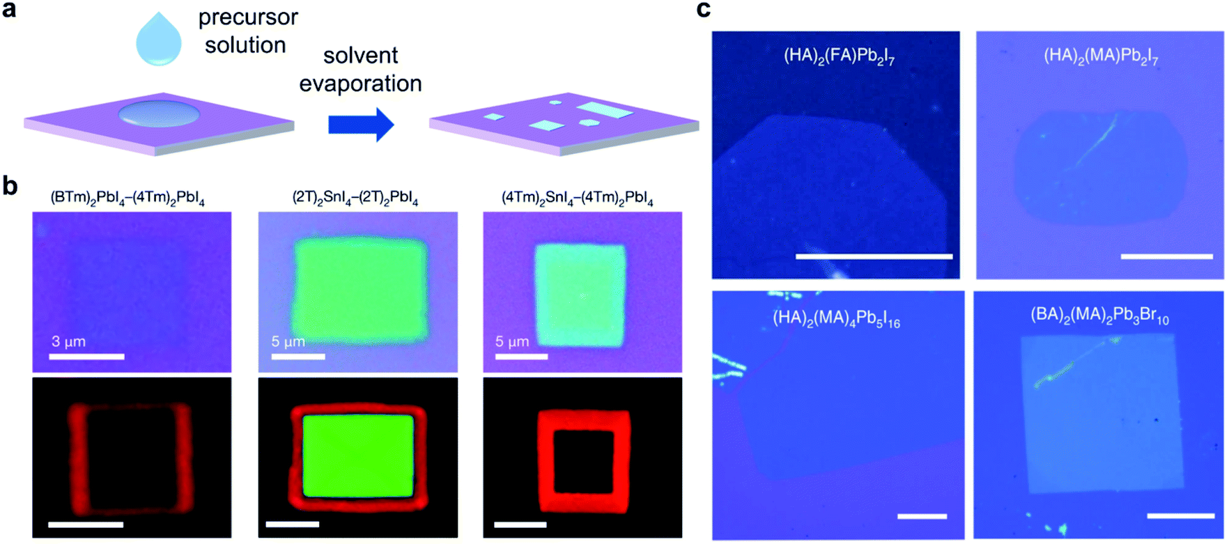 | ||
| Fig. 5 Synthesis and morphology of perovskite nanosheets. (a) Schematic illustration of direct synthesis of 2D halide perovskite thin sheets. (b) Optical and PL images of (BTm)2PbI4-(4Tm)2PbI4, (2T)2SnI4-(2T)2PbI4 and (4Tm)2SnI4-(4Tm)2PbI4 heterostructures79 (Copyright: 2020, Nature). (c) Optical images of HA2FAPb2I7, HA2MAPb2I7, HA2MA4Pb5I16 and BA2MA2Pb3Br10 nanosheets (scale bars: 25 μm)80 (Copyright: 2021, Nature Nanotechnology). | ||
In order to directly synthesize quasi-2D nanosheets with n > 1, Pan et al.80 established a method which derived from a slow cooling method for bulk crystal growth. A series of large-area quasi-2D perovskite nanosheets with tunable compositions and well-defined shape were obtained (Fig. 5c). By transferring a small droplet of supernatant precursor solution (for quasi-2D halide perovskite bulk single crystals) onto a glass substrate, nucleation and growth of nanosheets happened immediately at the solution surface. The lateral scale of the as-grown quasi-2D perovskite nanosheets can reach tens of micrometres and sometimes even above 100 μm. These large-area and thin quasi-2D halide perovskite nanosheets were used to assemble a series of van der Waals heterostructures. Based on these heterostructures, the carrier diffusion across the interface was studied, implying that carriers would transfer from a lower n phase to a higher n phase due to the type-I band alignment.
In addition to the above solution-processing strategies,81 the chemical vapor deposition (CVD) method, which is a conventional way to obtain ultrathin 2D materials like transition metal dichalcogenides and graphene, offers another alternative. Chen et al.82 successfully transformed pure-2D BA2PbBr4 (n = 1) into quasi-2D BA2MAn−1PbnBr3n+1 (n > 1) crystals through a CVD process. During this process, however, the MA cations are intercalated inside the perovskite lattice, introducing a very high density of lattice defects.
3.3 Thin films
Compared with bulk single crystals and nanosheets, quasi-2D halide perovskite thin films are most extensively utilized in electronic and optoelectronic devices. This is because of their ease in fabricating large-area, thickness-controllable thin film, which is compatible with the fabrication process of thin-film solar cells, LEDs and transistors.To make quasi-2D halide perovskite thin films, spin-coating and blade-coating processes are two common routes, as shown schematically in Fig. 6a and b. Distinct from single crystals and nanosheets, the phases in thin films are more complicated due to their polycrystalline nature. One thing that needs to be noted is that quasi-2D halide perovskite thin films consist of mixed 2D perovskite phases with different n values. The claimed n value of quasi-2D halide perovskite thin films in the reported literature always denotes the dominating n value or is determined by the stoichiometry of the added precursors. As shown in Fig. 6c, the absorption spectra of thin films possess multiple peaks compared with those of exfoliated single crystals. For example, the absorption spectra of (BA)2MA2Pb3I10 (n = 3) thin films exhibit an excitonic absorption peak at around 2.15 eV for n = 2 perovskite and an excitonic absorption peak at around 2.05 eV for n = 3 perovskite (Fig. 6c). Furthermore, the PL emission spectra of n = 3, 4, 5 thin films are very close, and all the peak positions apparently deviate from their corresponding intrinsic PL emissions determined from the single crystals83 (Fig. 6d). The full width at half maximum (FWHM) of PL peaks of thin films is also substantially broader than that of exfoliated single crystals. All of this indicates a rise in defects and poor phase purity in thin films.
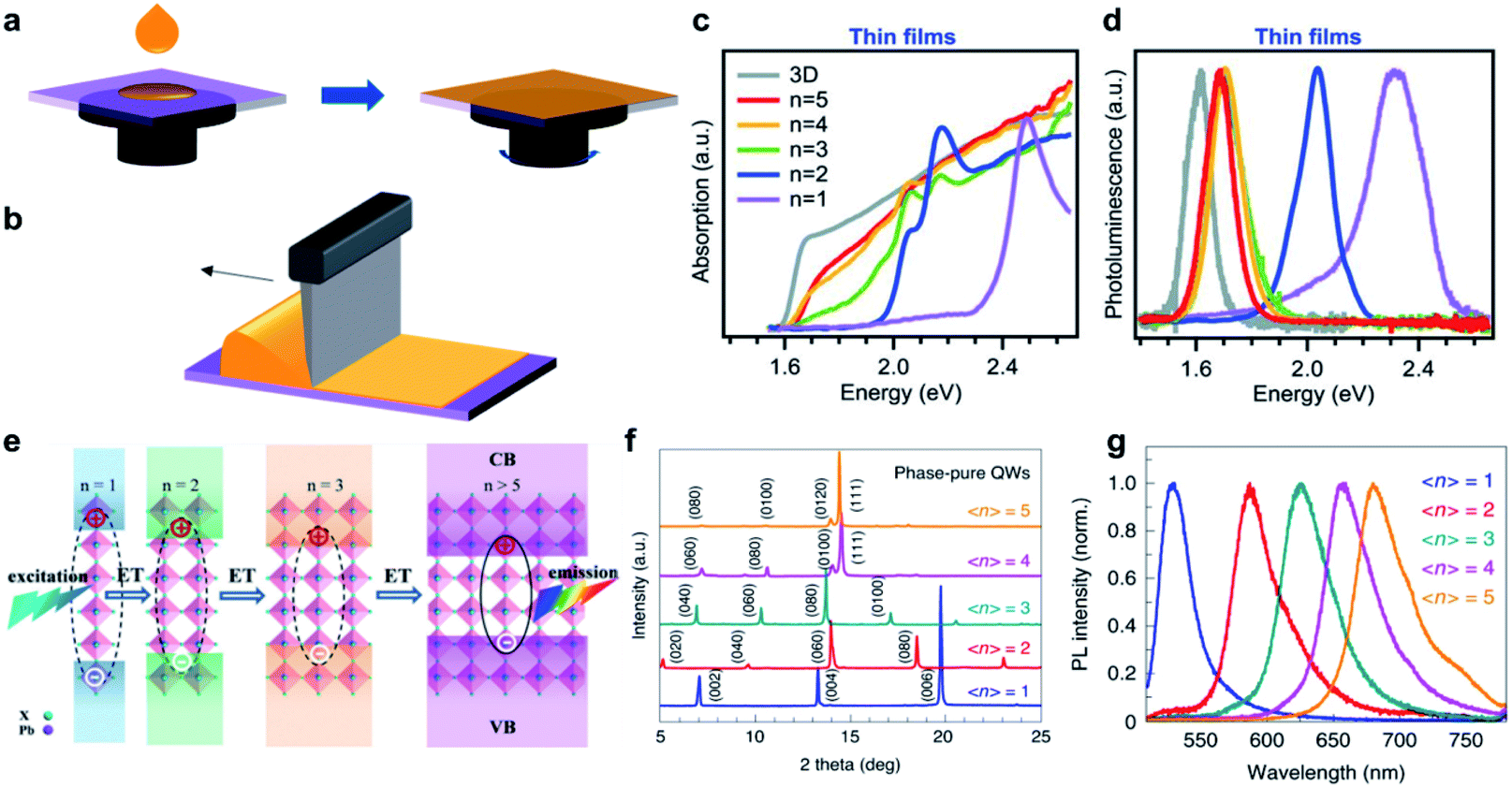 | ||
| Fig. 6 Quasi-2D perovskite thin film fabrication and their multi-phase nature. Schematics of (a) spin-coating and (b) blade-coating methods. (c) Absorption and (d) PL spectra of BA2MAn−1PbnI3n+1 thin films83 (Copyright: 2017, Science). (e) Illustration of energy funnelling in polycrystalline thin films85 (Copyright: 2018, Advanced Functional Materials). (f) XRD patterns and (g) normalized PL spectra of BA2MAn−1PbnI3n+1 thin films with improved purity87 (Copyright: 2020, Nature Energy). | ||
The multi-phase feature in thin films is further confirmed by ultrafast spectroscopy, based on which the carrier transfer between phases is studied. In (PEA)2MA2Pb3I10 (n = 3) thin films, four distinct PL peaks corresponding to n = 2, 3, 4 and 5 were observed in time-resolved PL measurements once the film was excited. Only PL emission of the smallest bandgap phase remained after about 500 ps.84 The carriers will transfer from a low n phase to the highest n phase because of the different bandgaps and type-I band alignment, called the energy funnelling effect85 (Fig. 6e). Along the out-of-plane direction, Zheng et al.86 proposed a distribution model for different phases within the quasi-2D halide perovskite thin films. The phases with lower n values were sandwiched by phases with higher n, facilitating carrier transport in the out-of-plane direction and making charge collection by the corresponding electrodes more efficient.
The above-mentioned energy funnelling effect indicates that the charges could be efficiently transferred between quasi-2D halide perovskites with different n values, highlighting the prospect of using quasi-2D halide perovskite materials as active semiconductors for next-generation optoelectronic devices. However, better phase purity quasi-2D halide perovskite thin films are required in order to gain thorough knowledge of the property–structure relationship. Therefore, plenty of research has been focused on synthesizing thin films with a narrow phase distribution and even pure phase via composition or solvent engineering. Liang et al.87 spin-coated a series of BA2MAn−1PbnI3n+1 thin films with different n values. They discovered that thin films with a nearly pure-phase could be achieved by substituting n-butylamine acetate (BAAc) for n-butylamine iodide (BAI). The XRD patterns of BAAc-based thin films are shown in Fig. 6f. In BAAc-based thin films, clear 2D crystallographic characteristic peaks can be observed, which contrasts sharply with BAI-based thin films. BAI-based thin films with n > 1 have several peaks in their PL spectra, indicating multiple phases with varied n values, while in BAAc-based thin films, nearly single peak emission can be achieved, suggesting improved purity, though the FWHM of PL peaks are sort of broad and there are some shoulders in PL spectra (Fig. 6g).
3.4 Quantum dots
Quantum dots are considered ideal candidates for display technologies due to their tuneable light emission and high PL quantum yield. The synthesis of halide perovskite quantum dots with quantum confinement similar to RP-phase quasi-2D perovskites is mainly implemented via one-pot synthesis88,89 and top-down synthesis.90,91 In one-pot synthesis, the precursors dissolved in organic solvent are heated and stirred in round-bottom flasks. Oleic acid and oleylamine are commonly used in this method to confine the size of products. Then the products will be centrifuged and redispersed to obtain perovskite quantum dots in solution. By adjusting the molar ratio of precursors, quantum dots with different n values can be achieved. As for top-down synthesis, perovskite quantum dots can be prepared by sonication of as-synthesized bulk single crystals. Compared with bulk crystals, the PL peak of quantum dots will blue-shift sightly because of the size effect, further enlarging the emitting range of quasi-2D perovskites.3.5 Challenges
With the increase of the n value, the successful synthesis of highly pure quasi-2D halide perovskites becomes increasingly challenging, which is probably related to the crystal growth thermodynamics. Soe et al.46 reported that the formation enthalpy is positive when n > 5 in the BA2MAn−1PbnI3n+1 series. The components with lower n values are more favored since they are thermodynamically stable. What's more, with higher n values, the difference in formation energy between different quasi-2D halide perovskites becomes minor, making it difficult to separate the specified phase. In this case, the impact from the kinetics becomes outstanding, like the precise control of crystal growth conditions (mainly supersaturation). To prepare higher n perovskites, a suitable catalyst may be required to lower the activation energy of the desired high n perovskites and alter the reaction pathway.4. Application
Due to their superior optoelectronic capabilities, outstanding stability, and tunability, quasi-2D halide perovskites are widely employed in light-emitting diodes, solar cells, lasers, photodetectors, and other applications. In this section, we will review the application progress and highlight the challenge of quasi-2D halide perovskites for optoelectronic devices.4.1 Light-emitting diodes
2D perovskites have high photoluminescence quantum yield (PLQY) and the colour of PL emission can be tuned facilely by altering the composition or n value. As a result, 2D halide perovskites can achieve a wide colour range of light emission45 (Fig. 7a). Additionally, the relatively narrow FWHM of the emitting peak enables high colour purity. Therefore, 2D halide perovskites are considered the promising candidate for high-performance light-emitting diodes. By integrating red, blue and green LEDs, white electroluminescence (EL) emission can be achieved92 (Fig. 7b).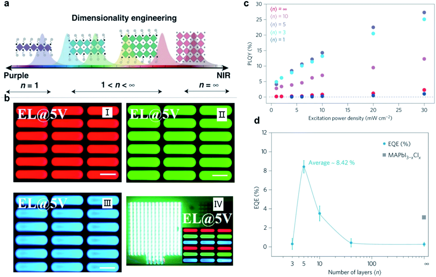 | ||
| Fig. 7 Colour tunability of quasi-2D perovskites and their application in light-emitting diodes. (a) n-Dependent PL colour tunability45 (Copyright: 2021, Light: Science & Applications). (b) EL image of RGB monochrome and white quasi-2D perovskite light-emitting diodes (scale bars: 100 μm)92 (Copyright: 2021, ACS Applied Materials & Interfaces). (c) The relationship between PLQY and excitation power density of (PEA)2MAn−1PbnI3n+1 with different n values86 (Copyright: 2016, Nature Nanotechnology). (d) External quantum efficiency as a function of n value84 (Copyright: 2016, Nature Nanotechnology). | ||
Compared with quasi-2D and 3D halide perovskites, pure-2D halide perovskites (n = 1) have the strongest quantum confinement and lowest dielectric screening effect. Therefore, nonradiative recombination in pure 2D halide perovskites is lowest because of their large exciton binding energy and short exciton diffusion length. From the perspective of PLQY (Fig. 7c), pure 2D halide perovskites have the top priority in the halide perovskite family.84 However, when pure-2D halide perovskites are applied as the active layer in a LED, the charge transport will be obstructed at low voltages caused by the large quantity of insulating organic ligands.93 LEDs based on quasi-2D perovskites are supposed to improve this situation.
An early LED based on quasi-2D perovskites in the visible region was fabricated using PEA2MAn−1PbnBr3n+1 (n = 1–4), and showed a brightness of 2935 cd m−2 and a PLQY of 34%.93 Yuan et al.84 extended the emission range to the near-infrared region using PEA2MAn−1PbnI3n+1 thin films. They compared the performance of devices using quasi-2D perovskites as emissive layers with n = 3, 5, 10, 40 and ∞, respectively (Fig. 7d). The device with n = 5 showed the highest external quantum efficiency (EQE) of 8.42% on average. As the n value increased, the EQE of devices with n > 5 declined. Up to now, the highest EQE of LEDs based on quasi-2D perovskite is 28.1% using PEA2Cs4Pb5Br16.94
4.2 Solar cells
Halide perovskite is one of the promising candidates for next-generation solar cells. Despite the tremendous progress, numerous obstacles remain, one of which is the poor stability of 3D halide perovskites, impeding the commercialization of halide perovskite solar cells.One proposed solution to this problem is to replace 3D perovskites with quasi-2D perovskites. The metal-halide octahedra in quasi-2D perovskites are better protected from moisture and oxygen by hydrophobic organic ligands. The organic ligands can also diminish metal-halide octahedron distortion and prevent phase transition, owing to their steric hindrance. Another advantage of quasi-2D halide perovskites is the ability to efficiently suppress anionic migration.
Smith et al.95 fabricated solar cells based on quasi-2D perovskites for the first time using (PEA)2MA2Pb3I10 as the absorption material with a power conversion efficiency (PCE) of 4.73% and open-circuit voltage (VOC) of 1.18 V. These devices showed much lower PCE but higher VOC compared with their 3D perovskite counterparts, which results from higher bandgap originating from the quantum well structure. Quan et al.96 fabricated 2D perovskite solar cells based on the (PEA)2MAn−1PbnI3n+1 series with n = 1, 2, 3, 6, 10, 40, 60 and ∞. The impact of quantum-well thickness (n value) was studied systematically in their work. As previously stated, the n value here was confirmed by stoichiometry in the precursors. The short-circuit current density (JSC) of devices is shown to increase as n increases, while the VOC decreases (Fig. 8a). This can be attributed to the limited carrier mobility in low-n quasi-2D perovskites, where the influence of organic ligands will strongly hinder the carrier transport. Meanwhile, in quasi-2D perovskites with high n, the strength of the binding energy is relatively weak, resulting in better carrier transport. Low carrier mobility would cause carrier accumulation, leading to high VOC but low JSC. The PCE showed a positive correlation with n (Fig. 8b). The PCE of those with n > 40 was almost twice that with n = 6. The bandgap of quasi-2D perovskites become narrower with the increase of n. In quasi-2D perovskites with low n, the wide bandgap would lead to insufficient absorption of the solar spectrum especially in the near-infrared range. In a stability test, devices based on 2D perovskites with low n showed less degradation after 1440 hours because of the strong protection from the organic ligands (Fig. 8c). On the other hand, the performance for low n was still lower than for n = 40 due to the poor initial performance.
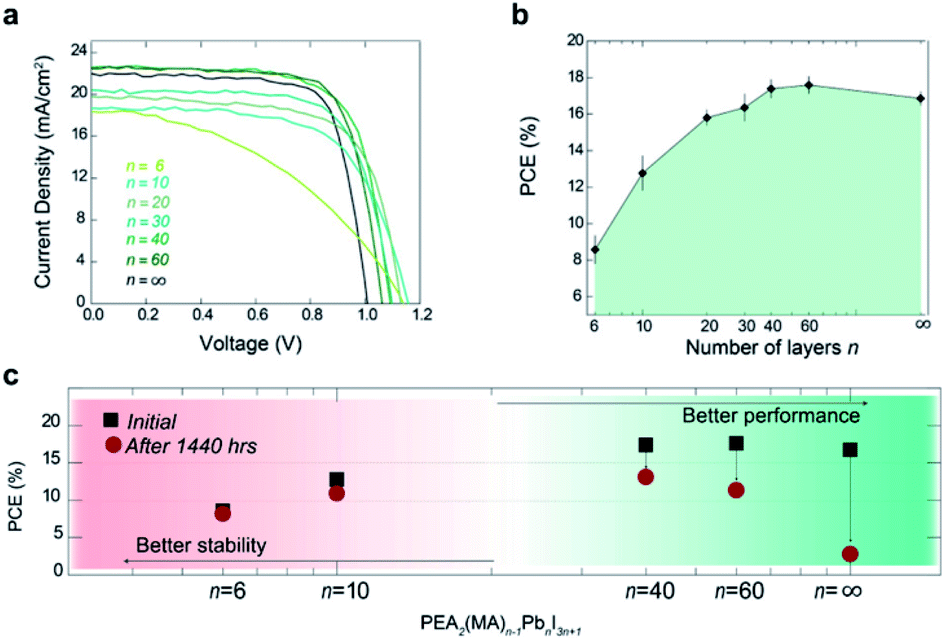 | ||
| Fig. 8 n-Dependence of quasi-2D halide perovskite solar cell performance. (a) J–V curves of solar cells based on PEA2MAn−1PbnI3n+1 (n = 5, 10, 20, 30, 40, 60 and ∞). (b) Power conversion efficiency and (c) stability versus n.96 (Copyright: 2016, Journal of the American Chemical Society). | ||
The performance of the quasi-2D perovskite solar cells is also related to the orientation of the grains. Compared with the in-plane direction, the conductivity will have a sharp decrease in the out-of-plane direction because of the dielectric organic ligands. In layer-by-layer devices like LEDs and solar cells, this problem will block the carrier transfer in the out-of-plane direction, leading to low performance of devices. One strategy is to alter the crystallographic orientation to make the grains grow vertically. In this way, charge transport and mobility in the out-of-plane direction will be significantly enhanced, resulting in much improved JSC and fill factor.97 Previous reports showed that the perpendicular heterogeneous nucleation occurring at the liquid–air interface is the origin of vertical orientation.98 During the crystal growth process, a low supersaturation condition is required to maintain continuous crystal growth along the vertical direction without any other nucleation.99 In devices fabrication, the adjustment of supersaturation can be achieved by controlling the rate of solvent evaporation, and more specifically, by controlling the additive type100,101 and quantity,102 solvent ratio,103,104 and substrate preheating temperature.97
As previously discussed in thin films, there are various co-existing phases with different n values and the proposed energy funnelling effect plays an important role in highly efficient carrier transport, making it difficult to specify the contributions from each phase or other interplay factors such as the energy funnelling effect. In addition, the film-forming conditions have an impact on the dominating n value, therefore the same recipe may correlate with different dominating n values in the final film. To achieve solar cells with near-limit PCE, further understanding of the relationship between the n value and photovoltaic properties is essential. To this end, developing new techniques to precisely control the n value within the quasi-2D halide perovskite thin films is of great significance.
4.3 Laser
In addition to LEDs and solar cells, quasi-2D halide perovskites are also promising gain materials for low-threshold continuous wave lasers.In quasi-2D perovskite thin films, amplified spontaneous emission (ASE), necessary for lasing, can be observed. It was reported that (NMA)2FAPb2BrxI7−x thin film showed an ultralow ASE threshold less than 20.0 ± 2 μJ cm−2, with outstanding optical stability (more than 32 hours).85 Using the same organic ligand, room-temperature continuous-wave lasing was achieved by Qin et al.15 Compared with (PEA)2FA7Pb8Br25, (NMA)2FA7Pb8Br25 thin film showed superior optical stability, which was attributed to the lower triplet exciton energy in the NMA-based perovskite (Fig. 9a). They demonstrated that annihilation of singlet–triplet excitons induced by long-lived triplet excitons reduces the quantity of photons, preventing population inversion. By employing distributed-feedback cavity and triplet management, room-temperature continuous-wave lasing was realized both in PEA-based and NMA-based perovskite thin films. Recent reports indicate that the lasing behaviour in thin films is primarily due to the energy funnelling effect.13,85,105–108 Zhai et al.108 studied the impact from phase segregation in PEA2Cs2Pb3Br10 thin films and found that the lasing phenomenon only happened in the multi-phase region, with a threshold of ∼500 μJ cm−2. Apart from thin films, lasing was also observed in quasi-2D perovskite polycrystalline nanowires and rings.12,38
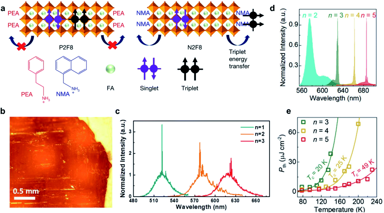 | ||
| Fig. 9 Lasers based on quasi-2D halide perovskites. (a) Chemical structure and triplet energy transport of PEA-based and NMA-based quasi-2D perovskites15 (Copyright: 2020, Nature). (b) The bottom surface of a millimetre-sized (BA)2PbI4 single crystal63 (Copyright: 2018, Nano Letters). (c) Lasing with different wavelengths in (BA)2(MA)n−1PbnI3n+1 quasi-2D perovskites63 (Copyright: 2018, Nano Letters). (d) Lasing spectra of exfoliated (BA)2(MA)n−1PbnI3n+1 single crystals at 77 K (ref. 109) (Copyright: 2019, Advanced Materials). (e) Temperature dependence of lasing thresholds of exfoliated (BA)2(MA)n−1PbnI3n+1 single crystals109 (Copyright: 2019, Advanced Materials). | ||
As opposed to multi-phase materials, lasing is also observed in pure-phase single crystals. Recent discoveries suggest that quasi-2D perovskite single crystals are a superior alternative to elucidate the fundamental physical mechanisms and realize ultralow threshold lasers. Raghavan et al.63 reported millimetre-sized (BA)2(MA)n−1PbnI3n+1 (n = 1, 2, 3) single crystals with a quite low lasing threshold ranging from 2.85 to 3.21 μJ cm−2 (Fig. 9b and c). Such low lasing thresholds result from the stepped-pyramidal morphology and the large refractive index difference between air and perovskite.
Subsequently, to explore the quasi-2D perovskites' applications in low-power consumption and chip-level coherent light sources for optoelectronic applications and better understand the microlasing in homologous quasi-2D perovskites, Liang et al.109 studied the ASE and lasing behaviours of mechanically exfoliated (BA)2(MA)n−1PbnI3n+1 thin crystals. Unlike the situation in uniform bulk single-crystals discussed above, the ASE phenomenon was only observed in the perovskites with n = 3, 4 and 5 (Fig. 9d). As shown in Fig. 9e, the increase of the n value resulted in the decrease of the lasing threshold, both in pump laser intensity and temperature. The underlying mechanism of this trend may lie in the enhanced Auger recombination and stronger exciton–phonon interaction in the lower n phase, which extensively constrained the optical gain in 2D perovskites.
According to the discussion above, high-n value and high-quality quasi-2D perovskite single crystals exhibit huge potential as a candidate for highly stable lasers with ultralow threshold and ultra-narrow lasing FWHM.
4.4 Photodetectors
Quasi-2D perovskites also show fascinating performance in photodetectors with high photoresponsivity, detectivity and response rate. To fabricate high-performance photodetectors, the coexistence of high responsivity, detectivity and response rate is essential. However, there is a dilemma that high photocurrent necessitates highly crystalline materials with effective conductivity, but dark current suppression necessitates a large number of defects to prevent thermally excited carriers from being transported.To confront this challenge, Feng et al.16 took advantage of the anisotropy and unique low-energy edge states of quasi-2D perovskites to selectively suppress the dark current. They fabricated nanowire-based photodetectors (Fig. 10a) using BA2MAn−1PbnI3n+1 (n = 2–5), and controlled the crystal orientation to make the wire length perpendicular to the perovskite layers and the spatially confined height and width parallel to the perovskite layer. Under illumination, the tightly bound excitons generated at the bulk nanowires will transfer to and dissociate efficiently in trace amounts of exposed layer edges, enabling photocarriers to be generated at the bulk nanowires but conduct at the edges. Furthermore, as a result of the unidirectional flow from the bulk to the surface, the photocarriers will directly establish contact with the top-contact electrodes (Fig. 10b). In this way, it is possible to achieve both a high resistance for dark current suppression and a high-photoconductivity channel. In addition, the impact of the n value on photodetector performance was examined in their research. From n = 2 to n = 4, the dark currents show a slight increase while the photocurrents significantly improve (Fig. 10c and d). Compared with quasi-2D crystals (n = 2), the superior photocurrent and responsivity of the higher n perovskite photodetector may originate from efficient exciton dissociation, carrier conduction and charge injection at crystallite edges. The best-performing devices (n = 4) show high responsivities of 1.5 × 10⁴![[thin space (1/6-em)]](https://www.rsc.org/images/entities/char_2009.gif) A W−1, detectivities of 7 × 10¹⁵ Jones and response time of 25μs. The slight drop of performance in n = 5 devices compared with n = 4 devices may be caused by less suppression of dark current from fewer organic barriers and higher defect density.
A W−1, detectivities of 7 × 10¹⁵ Jones and response time of 25μs. The slight drop of performance in n = 5 devices compared with n = 4 devices may be caused by less suppression of dark current from fewer organic barriers and higher defect density.
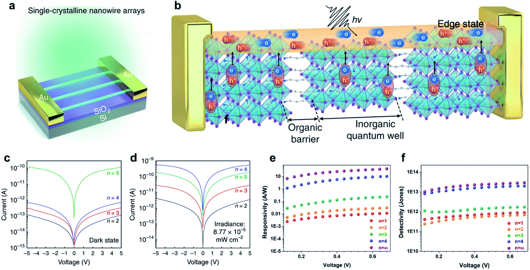 | ||
| Fig. 10 Photodetectors based on quasi-2D halide perovskites. (a) Device structure of quasi-2D photodetectors based on single crystalline nanowire arrays. (b) Carrier dynamics in quasi-2D photodetectors based on single crystalline nanowire arrays. The I–V curves of (BA)2(MA)n−1PbnI3n+1 quasi-2D perovskites in (c) the dark state and under (d) light illumination16 (Copyright: 2018, Nature Electronics). (e) Photocurrent and (f) responsivity versus voltage55 (Copyright: 2018, ACS Nano). | ||
Meanwhile, the same n-dependent performance can be seen in photodetectors with exfoliated crystals (Fig. 10e and f), which also show ultrasensitive detectivity.17,55,73
5. Conclusions and perspectives
In summary, pure-2D perovskites possess better stability, and larger exciton binding energy and bandgap, while 3D perovskites possess higher carrier mobility, longer carrier lifetime and smaller bandgap. From the perspective of crystal structure, quasi-2D halide perovskites can be viewed as the heterostructures stacked by repeated pure-2D and 3D halide perovskites. Compared with their pure-2D and 3D counterparts, quasi-2D perovskites provide a compromise in properties and a possibility for diverse high-performance applications (such as LEDs, solar cells, etc.) and could potentially integrate the merits from both pure-2D and 3D halide perovskites.On the other hand, from the perspective of materials science, the biggest challenge for the quasi-2D halide perovskite area is how to precisely control the n value in the single-crystal or polycrystalline material forms, and how to establish the relationship between the optoelectronic/electronic/ferroelectric properties and the specific structural parameters, such as n value, A-site cations and L-site organic ligands, etc. Because of the growth thermodynamics, the synthesis of high n 2D perovskites with high phase purity is quite tricky and challenging. In addition, tin (Sn)-based perovskites possess a smaller bandgap and higher carrier mobility compared with their Pb-based counterparts. However, in Sn-based perovskites, the Sn2+ will be easily oxidized into Sn4+, causing the destruction of perovskite structure and degradation of corresponding devices, which causes difficulties in the fundamental and application studies of Sn-based quasi-2D halide perovskites.
Based on the current research progress, we propose the following synthetic strategies for achieving high-purity quasi-2D Pb-based and Sn-based halide perovskite crystals:
1. Composition engineering via organic ligand selection and incorporation. Previous efforts suggest that the ligands will affect the preferred distribution of n value. Conjugated organic ligands with strong van der Waals interaction with their organic neighbours may be helpful to stabilize higher n structure. In addition, as the bulky organic ligands can improve the environmental stability of halide perovskites and suppress the anionic migration, the high-throughput selection and incorporation of appropriate bulky organic ligands into quasi-2D halide perovskite lattices may bring new opportunities to control the n value and stabilize sensitive perovskites such as Sn-based quasi-2D halide perovskites.
2. Mechanochemistry. In mechanochemistry, the reaction energy is provided by mechanical force. This method can avoid the use of solvent and provide a relatively pure reaction environment. Compared with the solution method, effects from solvent can be avoided, hence providing a possible approach to synthesize high-n quasi-2D halide perovskites with high phase purity.
3. Catalysts. Though n > 5 quasi-2D perovskites are not as thermodynamically stable as pure-2D and n < 5 quasi-2D perovskites, effective catalysts may alter the dynamic process, allowing highly selective synthesis and precise control of the n value.
Based on the excellent properties and unique structure of high-purity quasi-2D halide perovskites, additional applications could be envisioned beyond the optoelectronic applications discussed above. For example, the non-centrosymmetry induced by the organic ligands in pure-2D and quasi-2D halide perovskites will lead to the in-plane ferroelectricity within these materials. And there is discussion and assumption that the dipoles inside the halide perovskites brought by ferroelectrics could make the carrier separation more efficient, which might be one of the physical origins to justify the excellent photovoltaic performance of halide perovskite solar cells.110–116 Thus, a great variety of quasi-2D halide perovskites with tunable band structures provide a material platform to study the photovoltaic–ferroelectric correlation. Based on this, solar cells with higher efficiency might be achieved. In addition, as discussed above, Sn-based halide perovskites have lower bandgap and higher carrier mobility. Developing a high-purity quasi-2D halide perovskite with different n values and improved stability will provide more materials as candidates to develop high-performance Sn-based perovskite transistors and even ferroelectric transistors.
Conflicts of interest
There are no conflicts to declare.Notes and references
- M. Shao, T. Bie, L. Yang, Y. Gao, X. Jin, F. He, N. Zheng, Y. Yu and X. Zhang, Adv. Mater., 2022, 34, 2107211 CrossRef CAS PubMed.
- J. Liang, Z. Zhang, Q. Xue, Y. Zheng, X. Wu, Y. Huang, X. Wang, C. Qin, Z. Chen and C.-C. Chen, Energy Environ. Sci., 2022, 15, 296–310 RSC.
- W. Li, S. Sidhik, B. Traore, R. Asadpour, J. Hou, H. Zhang, A. Fehr, J. Essman, Y. Wang, J. M. Hoffman, I. Spanopoulos, J. J. Crochet, E. Tsai, J. Strzalka, C. Katan, M. A. Alam, M. G. Kanatzidis, J. Even, J. C. Blancon and A. D. Mohite, Nat. Nanotechnol., 2022, 17, 45–52 CrossRef CAS PubMed.
- X. Li, K. Li, B. X. Wang, X. N. Zhang, S. L. Yue, Y. X. Li, Q. Chen, S. L. Li, T. Yue, H. Q. Zhou and Y. Zhang, Adv. Funct. Mater., 2021, 31, 2107675 CrossRef CAS.
- Y. Zhang and N.-G. Park, ACS Energy Lett., 2022, 7, 757–765 CrossRef CAS.
- P. Pang, G. Jin, C. Liang, B. Wang, W. Xiang, D. Zhang, J. Xu, W. Hong, Z. Xiao, L. Wang, G. Xing, J. Chen and D. Ma, ACS Nano, 2020, 14, 11420–11430 CrossRef CAS PubMed.
- H. Chen, J. Lin, J. Kang, Q. Kong, D. Lu, J. Kang, M. Lai, L. N. Quan, Z. Lin, J. Jin, L. W. Wang, M. F. Toney and P. Yang, Sci. Adv., 2020, 6, eaay4045 CrossRef CAS PubMed.
- F. Yuan, X. Zheng, A. Johnston, Y. K. Wang, C. Zhou, Y. Dong, B. Chen, H. Chen, J. Z. Fan, G. Sharma, P. Li, Y. Gao, O. Voznyy, H. T. Kung, Z. H. Lu, O. M. Bakr and E. H. Sargent, Sci. Adv., 2020, 6, eabb0253 CrossRef CAS PubMed.
- Y. Liu, L. Zhang, S. Chen, C. Liu, Y. Li, J. Wu, D. Wang, Z. Jiang, Y. Li, Y. Li, X. Wang and B. Xu, Small, 2021, 17, 2101477 CrossRef CAS PubMed.
- Z. Guo, Y. Zhang, B. Wang, L. Wang, N. Zhou, Z. Qiu, N. Li, Y. Chen, C. Zhu, H. Xie, T. Song, L. Song, H. Xue, S. Tao, Q. Chen, G. Xing, L. Xiao, Z. Liu and H. Zhou, Adv. Mater., 2021, 33, 2102246 CrossRef CAS PubMed.
- A. D. Jodlowski, A. Yepez, R. Luque, L. Camacho and G. de Miguel, Angew. Chem., Int. Ed., 2016, 55, 14972–14977 CrossRef CAS PubMed.
- H. Zhang, Q. Liao, Y. Wu, Z. Zhang, Q. Gao, P. Liu, M. Li, J. Yao and H. Fu, Adv. Mater., 2018, 30, 1706186 CrossRef PubMed.
- M. R. Leyden, S. Terakawa, T. Matsushima, S. B. Ruan, K. Goushi, M. Auffray, A. S. D. Sandanayaka, C. J. Qin, F. Bencheikh and C. Adachi, ACS Photonics, 2019, 6, 460–466 CrossRef CAS.
- C. H. Lin, B. Cheng, T. Y. Li, J. R. D. Retamal, T. C. Wei, H. C. Fu, X. Fang and J. H. He, ACS Nano, 2019, 13, 1168–1176 CAS.
- C. Qin, A. S. D. Sandanayaka, C. Zhao, T. Matsushima, D. Zhang, T. Fujihara and C. Adachi, Nature, 2020, 585, 53–57 CrossRef CAS PubMed.
- J. G. Feng, C. Gong, H. F. Gao, W. Wen, Y. J. Gong, X. Y. Jiang, B. Zhang, Y. C. Wu, Y. S. Wu, H. B. Fu, L. Jiang and X. Zhang, Nat. Electron., 2018, 1, 404–410 CrossRef CAS.
- K. Leng, I. Abdelwahab, I. Verzhbitskiy, M. Telychko, L. Chu, W. Fu, X. Chi, N. Guo, Z. Chen, Z. Chen, C. Zhang, Q. H. Xu, J. Lu, M. Chhowalla, G. Eda and K. P. Loh, Nat. Mater., 2018, 17, 908–914 CrossRef CAS PubMed.
- Y. C. Liu, H. C. Ye, Y. X. Zhang, K. Zhao, Z. Yang, Y. B. Yuan, H. D. Wu, G. T. Zhao, Z. P. Yang, J. Tang, Z. Xu and S. Z. Liu, Matter, 2019, 1, 465–480 CrossRef.
- T. Ji, H. K. Zhang, N. Han, W. Y. Wang, B. Wu, G. H. Li, M. M. Fan, Z. F. Li, Y. Y. Hao, F. R. Zhu, Y. C. Wu and Y. X. Cui, J. Mater. Chem. C, 2020, 8, 1110–1117 RSC.
- S. Wang, Y. Chen, J. J. Yao, G. X. Zhao, L. Z. Li and G. F. Zou, J. Mater. Chem. C, 2021, 9, 6498–6506 RSC.
- C. Katan, N. Mercier and J. Even, Chem. Rev., 2019, 119, 3140–3192 CrossRef CAS PubMed.
- X. Han, Y. S. Zheng, S. D. Chai, S. H. Chen and J. L. Xu, Nanophotonics, 2020, 9, 1787–1810 CrossRef CAS.
- Y. K. Xu, M. Wang, Y. T. Lei, Z. P. Ci and Z. W. Jin, Adv. Energy Mater., 2020, 10, 2002558 CrossRef CAS.
- L. L. Gao, J. X. You and S. Z. Liu, J. Energy Chem., 2021, 57, 69–82 CrossRef.
- Y. S. Lei, Y. M. Chen and S. Xu, Matter, 2021, 4, 2266–2308 CrossRef CAS.
- S. N. Ruddlesden and P. Popper, Acta Crystallogr, 1958, 11, 54–55 CrossRef CAS.
- M. Dion, M. Ganne and M. Tournoux, Mater. Res. Bull., 1981, 16, 1429–1435 CrossRef CAS.
- A. J. Jacobson, J. W. Johnson and J. T. Lewandowski, Inorg. Chem., 2002, 24, 3727–3729 CrossRef.
- C. M. M. Soe, C. C. Stoumpos, M. Kepenekian, B. Traore, H. Tsai, W. Nie, B. Wang, C. Katan, R. Seshadri, A. D. Mohite, J. Even, T. J. Marks and M. G. Kanatzidis, J. Am. Chem. Soc., 2017, 139, 16297–16309 CrossRef CAS PubMed.
- N. Mercier, Angew. Chem., Int. Ed., 2019, 58, 17912–17917 CrossRef CAS PubMed.
- M. C. Weidman, M. Seitz, S. D. Stranks and W. A. Tisdale, ACS Nano, 2016, 10, 7830–7839 CrossRef CAS PubMed.
- Z. Wang, Y. Lu, Z. Xu, J. Hu, Y. Chen, C. Zhang, Y. Wang, F. Guo and Y. Mai, Adv. Sci., 2021, 8, e2101856 CrossRef PubMed.
- J. Zhang and B. Hu, Nano Energy, 2020, 76, 104999 CrossRef CAS.
- F. Wang, Z. Wang, W. Sun, Z. Wang, Y. Bai, T. Hayat, A. Alsaedi and Z. Tan, Small, 2020, 16, 2002940 CrossRef CAS PubMed.
- Y. Jin, Z. K. Wang, S. Yuan, Q. Wang, C. Qin, K. L. Wang, C. Dong, M. Li, Y. Liu and L. S. Liao, Adv. Funct. Mater., 2019, 30, 1908339 CrossRef.
- Y. Yang, S. Xu, Z. Ni, C. H. Van Brackle, L. Zhao, X. Xiao, X. Dai and J. Huang, Adv. Mater., 2021, 33, 2100783 CrossRef CAS PubMed.
- H. D. Lee, H. Kim, H. Cho, W. Cha, Y. Hong, Y. H. Kim, A. Sadhanala, V. Venugopalan, J. S. Kim, J. W. Choi, C. L. Lee, D. Kim, H. Yang, R. H. Friend and T. W. Lee, Adv. Funct. Mater., 2019, 29, 1901225 CrossRef.
- H. Zhang, Y. Wu, Q. Liao, Z. Zhang, Y. Liu, Q. Gao, P. Liu, M. Li, J. Yao and H. Fu, Angew. Chem., Int. Ed., 2018, 57, 7748–7752 CrossRef CAS PubMed.
- Y. Gao, E. Shi, S. Deng, S. B. Shiring, J. M. Snaider, C. Liang, B. Yuan, R. Song, S. M. Janke, A. Liebman-Pelaez, P. Yoo, M. Zeller, B. W. Boudouris, P. Liao, C. Zhu, V. Blum, Y. Yu, B. M. Savoie, L. Huang and L. Dou, Nat. Chem., 2019, 11, 1151–1157 CrossRef CAS PubMed.
- S. Silver, Q. Dai, H. Li, J. L. Brédas and A. Kahn, Adv. Energy Mater., 2019, 9, 1901005 CrossRef.
- J. A. Sichert, Y. Tong, N. Mutz, M. Vollmer, S. Fischer, K. Z. Milowska, R. Garcia Cortadella, B. Nickel, C. Cardenas-Daw, J. K. Stolarczyk, A. S. Urban and J. Feldmann, Nano Lett., 2015, 15, 6521–6527 CrossRef CAS PubMed.
- L. Polavarapu, B. Nickel, J. Feldmann and A. S. Urban, Adv. Energy Mater., 2017, 7, 1700267 CrossRef.
- J. Even, L. Pedesseau and C. Katan, ChemPhysChem, 2014, 15, 3733–3741 CrossRef CAS PubMed.
- R. Chakraborty and A. Nag, Phys. Chem. Chem. Phys., 2021, 23, 82–93 RSC.
- L. Zhang, C. Sun, T. He, Y. Jiang, J. Wei, Y. Huang and M. Yuan, Light. Sci. Appl., 2021, 10, 61 CrossRef CAS PubMed.
- C. M. M. Soe, G. P. Nagabhushana, R. Shivaramaiah, H. Tsai, W. Nie, J. C. Blancon, F. Melkonyan, D. H. Cao, B. Traore, L. Pedesseau, M. Kepenekian, C. Katan, J. Even, T. J. Marks, A. Navrotsky, A. D. Mohite, C. C. Stoumpos and M. G. Kanatzidis, Proc. Natl. Acad. Sci. U. S. A., 2019, 116, 58–66 CrossRef PubMed.
- J. Tauc, R. Grigorovici and A. Vancu, Phys. Status Solidi B, 1966, 15, 627–637 CrossRef CAS.
- S. Deng, E. Shi, L. Yuan, L. Jin, L. Dou and L. Huang, Nat. Commun., 2020, 11, 664 CrossRef CAS PubMed.
- W. Chen, Y. Shi, J. Chen, P. Ma, Z. Fang, D. Ye, Y. Lu, Y. Yuan, J. Zhao and Z. Xiao, Adv. Mater., 2021, 33, 2104842 CrossRef CAS PubMed.
- Z. Guo, X. Wu, T. Zhu, X. Zhu and L. Huang, ACS Nano, 2016, 10, 9992–9998 CrossRef CAS PubMed.
- S. Wang, J. Ma, W. Li, J. Wang, H. Wang, H. Shen, J. Li, J. Wang, H. Luo and D. Li, J. Phys. Chem. Lett., 2019, 10, 2546–2553 CrossRef CAS PubMed.
- D. Ghosh, A. J. Neukirch and S. Tretiak, J. Phys. Chem. Lett., 2020, 11, 2955–2964 CrossRef CAS PubMed.
- Y. Shao, W. Gao, H. Yan, R. Li, I. Abdelwahab, X. Chi, L. Rogee, L. Zhuang, W. Fu, S. P. Lau, S. F. Yu, Y. Cai, K. P. Loh and K. Leng, Nat. Commun., 2022, 13, 138 CrossRef CAS PubMed.
- A. Chernikov, T. C. Berkelbach, H. M. Hill, A. Rigosi, Y. Li, O. B. Aslan, D. R. Reichman, M. S. Hybertsen and T. F. Heinz, Phys. Rev. Lett., 2014, 113, 076802 CrossRef CAS PubMed.
- K. Wang, C. Wu, D. Yang, Y. Jiang and S. Priya, ACS Nano, 2018, 12, 4919–4929 CrossRef CAS PubMed.
- Akriti, E. Shi, S. B. Shiring, J. Yang, C. L. Atencio-Martinez, B. Yuan, X. Hu, Y. Gao, B. P. Finkenauer, A. J. Pistone, Y. Yu, P. Liao, B. M. Savoie and L. Dou, Nat. Nanotechnol., 2021, 16, 584–591 CrossRef CAS PubMed.
- Akriti, S. Zhang, Z. Y. Lin, E. Shi, B. P. Finkenauer, Y. Gao, A. J. Pistone, K. Ma, B. M. Savoie and L. Dou, Adv. Mater., 2021, 33, 2105183 CrossRef CAS.
- C. C. Stoumpos, D. H. Cao, D. J. Clark, J. Young, J. M. Rondinelli, J. I. Jang, J. T. Hupp and M. G. Kanatzidis, Chem. Mater., 2016, 28, 2852–2867 CrossRef CAS.
- C. C. Stoumpos, C. M. M. Soe, H. Tsai, W. Nie, J.-C. Blancon, D. H. Cao, F. Liu, B. Traoré, C. Katan, J. Even, A. D. Mohite and M. G. Kanatzidis, Chem, 2017, 2, 427–440 CAS.
- L. Mao, R. M. Kennard, B. Traore, W. Ke, C. Katan, J. Even, M. L. Chabinyc, C. C. Stoumpos and M. G. Kanatzidis, Chem, 2019, 5, 2593–2604 CAS.
- J. Wang, Y. Mi, X. Gao, J. Li, J. Li, S. Lan, C. Fang, H. Shen, X. Wen, R. Chen, X. Liu, T. He and D. Li, Adv. Opt. Mater., 2019, 7, 1900398 CrossRef.
- X. T. Li, Y. P. Fu, L. Pedesseau, P. J. Guo, S. Cuthriell, I. Hadar, J. Even, C. Katan, C. C. Stoumpos, R. D. Schaller, E. Harel and M. G. Kanatzidis, J. Am. Chem. Soc., 2020, 142, 11486–11496 CrossRef CAS PubMed.
- C. M. Raghavan, T. P. Chen, S. S. Li, W. L. Chen, C. Y. Lo, Y. M. Liao, G. Haider, C. C. Lin, C. C. Chen, R. Sankar, Y. M. Chang, F. C. Chou and C. W. Chen, Nano Lett., 2018, 18, 3221–3228 CrossRef CAS PubMed.
- X. Xiao, J. Dai, Y. Fang, J. Zhao, X. Zheng, S. Tang, P. N. Rudd, X. C. Zeng and J. Huang, ACS Energy Lett., 2018, 3, 684–688 CrossRef CAS.
- W. Paritmongkol, N. S. Dahod, A. Stollmann, N. N. Mao, C. Settens, S. L. Zheng and W. A. Tisdale, Chem. Mater., 2019, 31, 5592–5607 CrossRef CAS.
- J. Li, J. Wang, Y. Zhang, H. Wang, G. Lin, X. Xiong, W. Zhou, H. Luo and D. Li, 2D Mater., 2018, 5, 021001 CrossRef.
- S. Han, P. Wang, J. Zhang, X. Liu, Z. Sun, X. Huang, L. Li, C. Ji, W. Zhang, B. Teng, W. Hu, M. Hong and J. Luo, Laser Photonics Rev., 2018, 12, 1800060 CrossRef.
- M. Cinquino, L. Polimeno, G. Lerario, M. De Giorgi, A. Moliterni, V. Olieric, A. Fieramosca, S. Carallo, R. Mastria, V. Ardizzone, L. Dominici, D. Ballarini, C. Giannini, D. Sanvitto, A. Rizzo and L. De Marco, J. Lumin., 2020, 221, 117079 CrossRef CAS.
- M. Cinquino, A. Fieramosca, R. Mastria, L. Polimeno, A. Moliterni, V. Olieric, N. Matsugaki, R. Panico, M. De Giorgi, G. Gigli, C. Giannini, A. Rizzo, D. Sanvitto and L. De Marco, Adv. Mater., 2021, 33, 2102326 CrossRef CAS PubMed.
- J. Wang, J. Li, Q. Tan, L. Li, J. Zhang, J. Zang, P. Tan, J. Zhang and D. Li, J. Phys. Chem. Lett., 2017, 8, 6211–6219 CrossRef CAS PubMed.
- W. Peng, J. Yin, K. T. Ho, O. Ouellette, M. De Bastiani, B. Murali, O. El Tall, C. Shen, X. Miao, J. Pan, E. Alarousu, J. H. He, B. S. Ooi, O. F. Mohammed, E. Sargent and O. M. Bakr, Nano Lett., 2017, 17, 4759–4767 CrossRef CAS PubMed.
- G. Liu, J. Liu, Z. Fan, X. He, K. Luo, Q. Ye and C. Liao, Phys. Status Solidi RRL, 2021, 15, 2100099 CrossRef CAS.
- L. Li, Z. Sun, P. Wang, W. Hu, S. Wang, C. Ji, M. Hong and J. Luo, Angew. Chem., Int. Ed., 2017, 56, 12150–12154 CrossRef CAS PubMed.
- L. Li, X. Shang, S. Wang, N. Dong, C. Ji, X. Chen, S. Zhao, J. Wang, Z. Sun, M. Hong and J. Luo, J. Am. Chem. Soc., 2018, 140, 6806–6809 CrossRef CAS PubMed.
- E. S. Vasileiadou, I. Hadar, M. Kepenekian, J. Even, Q. Tu, C. D. Malliakas, D. Friedrich, I. Spanopoulos, J. M. Hoffman, V. P. Dravid and M. G. Kanatzidis, Chem. Mater., 2021, 33, 5085–5107 CrossRef CAS.
- C. Ji, Y. Li, X. Liu, Y. Wang, T. Zhu, Q. Chen, L. Li, S. Wang and J. Luo, Angew. Chem., Int. Ed. Engl., 2021, 60, 20970–20976 CrossRef CAS PubMed.
- N. Mercier, CrystEngComm, 2005, 7, 429–432 RSC.
- L. Dou, A. B. Wong, Y. Yu, M. Lai, N. Kornienko, S. W. Eaton, A. Fu, C. G. Bischak, J. Ma, T. Ding, N. S. Ginsberg, L. W. Wang, A. P. Alivisatos and P. Yang, Science, 2015, 349, 1518–1521 CrossRef CAS PubMed.
- E. Shi, B. Yuan, S. B. Shiring, Y. Gao, Akriti, Y. Guo, C. Su, M. Lai, P. Yang, J. Kong, B. M. Savoie, Y. Yu and L. Dou, Nature, 2020, 580, 614–620 CrossRef CAS PubMed.
- D. Pan, Y. Fu, N. Spitha, Y. Zhao, C. R. Roy, D. J. Morrow, D. D. Kohler, J. C. Wright and S. Jin, Nat. Nanotechnol., 2021, 16, 159–165 CrossRef CAS PubMed.
- R. Guo, Z. Zhu, A. Boulesbaa, F. Hao, A. Puretzky, K. Xiao, J. Bao, Y. Yao and W. Li, Small Methods, 2017, 1, 1700245 CrossRef.
- J. Chen, Y. Wang, L. Gan, Y. He, H. Li and T. Zhai, Angew. Chem., Int. Ed., 2017, 56, 14893–14897 CrossRef CAS PubMed.
- J. C. Blancon, H. Tsai, W. Nie, C. C. Stoumpos, L. Pedesseau, C. Katan, M. Kepenekian, C. M. Soe, K. Appavoo, M. Y. Sfeir, S. Tretiak, P. M. Ajayan, M. G. Kanatzidis, J. Even, J. J. Crochet and A. D. Mohite, Science, 2017, 355, 1288–1292 CrossRef CAS PubMed.
- M. Yuan, L. N. Quan, R. Comin, G. Walters, R. Sabatini, O. Voznyy, S. Hoogland, Y. Zhao, E. M. Beauregard, P. Kanjanaboos, Z. Lu, D. H. Kim and E. H. Sargent, Nat. Nanotechnol., 2016, 11, 872–877 CrossRef CAS PubMed.
- M. L. Li, Q. G. Gao, P. Liu, Q. Liao, H. H. Zhang, J. N. Yao, W. P. Hu, Y. S. Wu and H. B. Fu, Adv. Funct. Mater., 2018, 28, 1707006 CrossRef.
- F. Zheng, C. R. Hall, D. Angmo, C. Zuo, S. Rubanov, Z. Wen, S. J. Bradley, X.-T. Hao, M. Gao, T. A. Smith and K. P. Ghiggino, J. Mater. Chem. C, 2021, 9, 5362–5372 RSC.
- C. Liang, H. Gu, Y. Xia, Z. Wang, X. Liu, J. Xia, S. Zuo, Y. Hu, X. Gao, W. Hui, L. Chao, T. Niu, M. Fang, H. Lu, H. Dong, H. Yu, S. Chen, X. Ran, L. Song, B. Li, J. Zhang, Y. Peng, G. Shao, J. Wang, Y. Chen, G. Xing and W. Huang, Nat. Energy, 2020, 6, 38–45 CrossRef.
- Q. A. Akkerman, S. G. Motti, A. R. Srimath Kandada, E. Mosconi, V. D'Innocenzo, G. Bertoni, S. Marras, B. A. Kamino, L. Miranda, F. De Angelis, A. Petrozza, M. Prato and L. Manna, J. Am. Chem. Soc., 2016, 138, 1010–1016 CrossRef CAS PubMed.
- Y. H. Chang, J. C. Lin, Y. C. Chen, T. R. Kuo and D. Y. Wang, Nanoscale Res. Lett., 2018, 13, 247 CrossRef PubMed.
- S. J. Varma, J. Cherusseri, J. Li, J. Kumar, E. Barrios and J. Thomas, AIP Adv., 2020, 10, 045130 CrossRef CAS.
- J. Zhao, Z. Zheng, W. Liu, X. Tang, D. Jin and X. Wang, J. Mater. Sci.: Mater. Electron., 2020, 32, 12922–12928 CrossRef.
- J. Wang, D. Li, L. Mu, M. Li, Y. Luo, B. Zhang, C. Mai, B. Guo, L. Lan, J. Wang, H. L. Yip and J. Peng, ACS Appl. Mater. Interfaces, 2021, 13, 41773–41781 CrossRef CAS PubMed.
- J. Byun, H. Cho, C. Wolf, M. Jang, A. Sadhanala, R. H. Friend, H. Yang and T.-W. Lee, Adv. Mater., 2016, 28, 7515–7520 CrossRef CAS PubMed.
- Z. Liu, W. Qiu, X. Peng, G. Sun, X. Liu, D. Liu, Z. Li, F. He, C. Shen, Q. Gu, F. Ma, H.-L. Yip, L. Hou, Z. Qi and S.-J. Su, Adv. Mater., 2021, 33, 2103268 CrossRef CAS PubMed.
- I. C. Smith, E. T. Hoke, D. Solis-Ibarra, M. D. McGehee and H. I. Karunadasa, Angew. Chem., Int. Ed., 2014, 53, 11232–11235 CrossRef CAS PubMed.
- L. N. Quan, M. Yuan, R. Comin, O. Voznyy, E. M. Beauregard, S. Hoogland, A. Buin, A. R. Kirmani, K. Zhao, A. Amassian, D. H. Kim and E. H. Sargent, J. Am. Chem. Soc., 2016, 138, 2649–2655 CrossRef CAS PubMed.
- H. Tsai, W. Nie, J. C. Blancon, C. C. Stoumpos, R. Asadpour, B. Harutyunyan, A. J. Neukirch, R. Verduzco, J. J. Crochet, S. Tretiak, L. Pedesseau, J. Even, M. A. Alam, G. Gupta, J. Lou, P. M. Ajayan, M. J. Bedzyk and M. G. Kanatzidis, Nature, 2016, 536, 312–316 CrossRef CAS PubMed.
- A. Z. Chen, M. Shiu, J. H. Ma, M. R. Alpert, D. Zhang, B. J. Foley, D. M. Smilgies, S. H. Lee and J. J. Choi, Nat. Commun., 2018, 9, 1336 CrossRef PubMed.
- A. Z. Chen, M. Shiu, X. Deng, M. Mahmoud, D. Zhang, B. J. Foley, S.-H. Lee, G. Giri and J. J. Choi, Chem. Mater., 2019, 31, 1336–1343 CrossRef CAS.
- X. Zhang, G. Wu, W. Fu, M. Qin, W. Yang, J. Yan, Z. Zhang, X. Lu and H. Chen, Adv. Energy Mater., 2018, 8, 1702498 CrossRef.
- C. Lan, G. Liang, S. Zhao, B. Fan, H. Lan, H. Peng, H. Sun, D. Zhang, J. Luo and P. Fan, J. Am. Chem. Soc., 2019, 102, 4152–4160 CAS.
- X. Zhang, G. Wu, S. Yang, W. Fu, Z. Zhang, C. Chen, W. Liu, J. Yan, W. Yang and H. Chen, Small, 2017, 13, 1700611 CrossRef PubMed.
- L. Gao, F. Zhang, C. Xiao, X. Chen, B. W. Larson, J. J. Berry and K. Zhu, Adv. Funct. Mater., 2019, 29, 1901652 CrossRef CAS.
- A. Caiazzo, K. Datta, J. Jiang, M. C. Gelvez-Rueda, J. Li, R. Ollearo, J. M. Vicent-Luna, S. Tao, F. C. Grozema, M. M. Wienk and R. A. J. Janssen, Adv. Energy Mater., 2021, 11, 2102144 CrossRef CAS.
- M. Cui, C. Qin, Y. Jiang, M. Yuan, L. Xu, D. Song, Y. Jiang and Y. Liu, J. Phys. Chem. Lett., 2020, 11, 5734–5740 CrossRef CAS PubMed.
- L. Lei, D. Seyitliyev, S. Stuard, J. Mendes, Q. Dong, X. Fu, Y.-A. Chen, S. He, X. Yi, L. Zhu, C.-H. Chang, H. Ade, K. Gundogdu and F. So, Adv. Mater., 2020, 32, 1906571 CrossRef CAS PubMed.
- M. R. Leyden, T. Matsushima, C. Qin, S. Ruan, H. Ye and C. Adachi, Phys. Chem. Chem. Phys., 2018, 20, 15030–15036 RSC.
- W. Zhai, C. Tian, K. Yuan, C. Ge, S. Zhao, H. Yu, Y. Li, W. Chen and G. Ran, Appl. Phys. Lett., 2019, 114, 131107 CrossRef.
- Y. Liang, Q. Shang, Q. Wei, L. Zhao, Z. Liu, J. Shi, Y. Zhong, J. Chen, Y. Gao, M. Li, X. Liu, G. Xing and Q. Zhang, Adv. Mater., 2019, 31, 1903030 CrossRef PubMed.
- K. S. Nalwa, J. A. Carr, R. C. Mahadevapuram, H. K. Kodali, S. Bose, Y. Q. Chen, J. W. Petrich, B. Ganapathysubramanian and S. Chaudhary, Energy Environ. Sci., 2012, 5, 7042–7049 RSC.
- H. S. Kim, S. K. Kim, B. J. Kim, K. S. Shin, M. K. Gupta, H. S. Jung, S. W. Kim and N. G. Park, J. Phys. Chem. Lett., 2015, 6, 1729–1735 CrossRef CAS PubMed.
- P. Wang, J. Zhao, L. Wei, Q. Zhu, S. Xie, J. Liu, X. Meng and J. Li, Nanoscale, 2017, 9, 3806–3817 RSC.
- L. You, F. Zheng, L. Fang, Y. Zhou, L. Z. Tan, Z. Zhang, G. Ma, D. Schmidt, A. Rusydi, L. Wang, L. Chang, A. M. Rappe and J. Wang, Sci. Adv., 2018, 4, eaat3438 CrossRef PubMed.
- L. Qiao, W. H. Fang and R. Long, J. Phys. Chem. Lett., 2019, 10, 7237–7244 CrossRef CAS PubMed.
- C. C. Zhang, Z. K. Wang, S. Yuan, R. Wang, M. Li, M. F. Jimoh, L. S. Liao and Y. Yang, Adv. Mater., 2019, 31, 1902222 CrossRef PubMed.
- T. Kumari, S. Jung, Y. Cho, H.-P. Kim, J. W. Lee, J. Oh, J. Lee, S. M. Lee, M. Jeong, J. M. Baik, W. Jo and C. Yang, Nano Energy, 2020, 68, 104327 CrossRef CAS.
| This journal is © The Royal Society of Chemistry 2022 |