DOI:
10.1039/D2TA01926D
(Review Article)
J. Mater. Chem. A, 2022,
10, 19129-19168
Controlled local orientation of 2D nanomaterials in 3D devices: methods and prospects for multifunctional designs and enhanced performance
Received
10th March 2022
, Accepted 25th April 2022
First published on 26th April 2022
Abstract
Two-dimensional (2D) nanomaterials are sheet-like crystalline solids exhibiting remarkable electrical, chemical, mechanical and optical properties. The emergence of 2D nanomaterials of diverse chemistries with unique performance at the nanometric scale provides great potential to establish enhanced functionalities at the macroscopic scale. However, transposing these nanoscopic properties into functional macroscopic devices remains a challenge due to the lack of suitable processing technologies. Recent experimental efforts to control the local orientation of 2D materials in thin films and reinforced composites have demonstrated significant advances in improving the bulk material performances and could be the key to unlocking next-generation multifunctional designs. Examples of these for sensors, thermoelectrics and energy harvesting devices are provided in this review. Then, we present the recent advances and methods for achieving controlled alignment of 2D nanomaterials, including in horizontal, vertical, heterogeneous and arbitrarily oriented configurations. Moreover, the advances in 3D printing technology to support aligned microstructures and its capability to build multimaterial compositions, design complex structures and scale up are discussed in detail. Finally, we envision exciting future developments yet also challenges to realize the promise of complex multifunctional energy devices based on 2D nanomaterials with enhanced performance and sustainability, potentially opening up new applications.
 Hongying He | Hongying He received her BS degree from Sichuan University, China, in 2016. Afterwards, she received her PhD degree in Mechanical Engineering from the National University of Singapore (NUS) in 2020. She is currently a research fellow in the School of Mechanical and Aerospace Engineering at Nanyang Technological University in Singapore. Her research interests focus on ceramic-based composite structural design for thermal management and study of lead-free ferroelectric ceramics and their functional applications. |
 Lizhi Guan | Lizhi Guan received his PhD in Applied Chemistry from the Instituto de Ciencia de Materiales de Madrid (ICMM, CSIC) and Autonomous University of Madrid, Spain (2020). After that, he joined the School of Mechanical and Aerospace Engineering at Nanyang Technological University in Singapore as a research fellow. His research interests mainly include bioinspired carbon-based composites with multifunctional properties. |
 Hortense Le Ferrand | Hortense Le Ferrand is a Nanyang Assistant Professor in the School of Mechanical and Aerospace Engineering and School of Materials Science and Engineering at Nanyang Technological University in Singapore, where she leads the Laboratory for Dense Multifunctional Composites (LDMC). She received her PhD degree in Materials Science from the Swiss Federal Institute of Technology (ETH Zürich) in Switzerland in 2017. Dr Le Ferrand is the recipient of the prestigious National Research Foundation Fellowship (2020) from Singapore. Her research focuses on novel additive manufacturing technologies for dense composites, microstructural designs and fabrication of bio-inspired composite and ceramic materials for combined structural and functional properties. |
1. Introduction
Multifunctional devices are objects able to achieve a combined set of properties, such as electrical, mechanical, optical, or thermal, and that are able to convert energy from one type to another. Electronic components, sensors, energy harvesting and water splitting devices, and catalyzers are examples of devices receiving great interest from both the scientific community and industries, and they require the fusion of multiple properties into one object. More recently, robotics, automobiles, artificial intelligence (AI), and the Internet of Things (IoT) have increasingly relied on multifunctional devices that are smaller, faster, high performing, and processable into 3D shapes by 3D printing. The rapid technological growth in these domains reflects the unprecedented advances in materials science and engineering and urges further material evolution on both functional and structural aspects. To fulfill these versatile functionalities and realize the promise of Industry 4.0, 2D nanomaterials which exhibit unique intrinsic properties have become an indispensable choice.
2D nanomaterials are a class of crystalline materials in the form of a single-layer or a few-layer lamellar structure. They possess a high lateral diameter to thickness aspect ratio as well as stronger in-plane interatomic interactions than in their stacking, out-of-plane direction. The year of 2004 witnessed the successful exfoliation of monolayer graphene by Geim and Novoselov,1 which led to the renaissance of the study of 2D nanolayer materials. Since then, remarkable properties such as a large surface area, tunable surface functionality, strong mechanical strength, and excellent thermal and electrical conductivities have been successively found in graphene.2–11 Notably, these outstanding properties in graphene such as its ultrahigh carrier mobility of 104 cm2 V−1 s−1, thermal conductivity of about 4000 W m−1 K−1 and high Young's modulus of about 1 TPa are demonstrated in the in-plane direction, which are significantly suppressed along the out-of-plane axis.12–14 The preparation of 2D nanomaterials is commonly achieved by top-down approaches, where bulk layered materials are exfoliated into nanosheets for example using mechanochemical processes or by bottom-up synthesis from molecular precursors. More recently, the prosperous studies on graphene have expanded to the emergence of novel 2D nanomaterials of other chemistries.15 For example, transition metal dichalcogenides (TMDCs), with the formula of MX2, where M is a transition metal like Mo, Ti, V, Hf, W, etc., and X represents a chalcogen such as S, Te and Se, have been found to exhibit tunable bandgaps for semiconducting and optoelectronic related applications.6,16,17 In addition, 2D hexagonal boron nitride (h-BN), an isomorph of graphene, also attracts considerable attention. Indeed, different from the conjugated valence electrons in graphite, the distinct electronegativity of B and N atoms provides electrical insulation to h-BN.18 Thanks to its outstanding electrical insulation, an in-plane thermal conductivity of about 400 W m−1 K−1, thermal stability at temperatures higher than 600 °C, mechanical robustness and chemical inertness, 2D h-BN becomes very useful for microelectronics, as a reinforcing nanofiller and field effect transistor (FET), among others.19,20 Moreover, the family of MXenes, which represents 2D transition metal carbides, nitrides and carbonitrides, has grown rapidly over the past decade.21–23 MXenes have a general formula of Mn+1XnTx (n = 1–3), where M is a transition metal such as Ti, Ta, V, Zr, etc., X is carbon or nitrogen, and Tx represents surface functional groups. Since the report of Ti3C2 in 2011, there have been more than 30 different MXenes synthesized, which typically exhibit metallic conductive properties because of the existence of conductive carbon and metal layers in the 2D structure and a hydrophilic nature due to the surface terminations like hydroxyl, oxygen or fluorine.21,24,25 The wide chemical and structural variety of MXenes enables their promising applications for energy storage, electromagnetic interference (EMI) shielding, catalysis, sensors and so on.
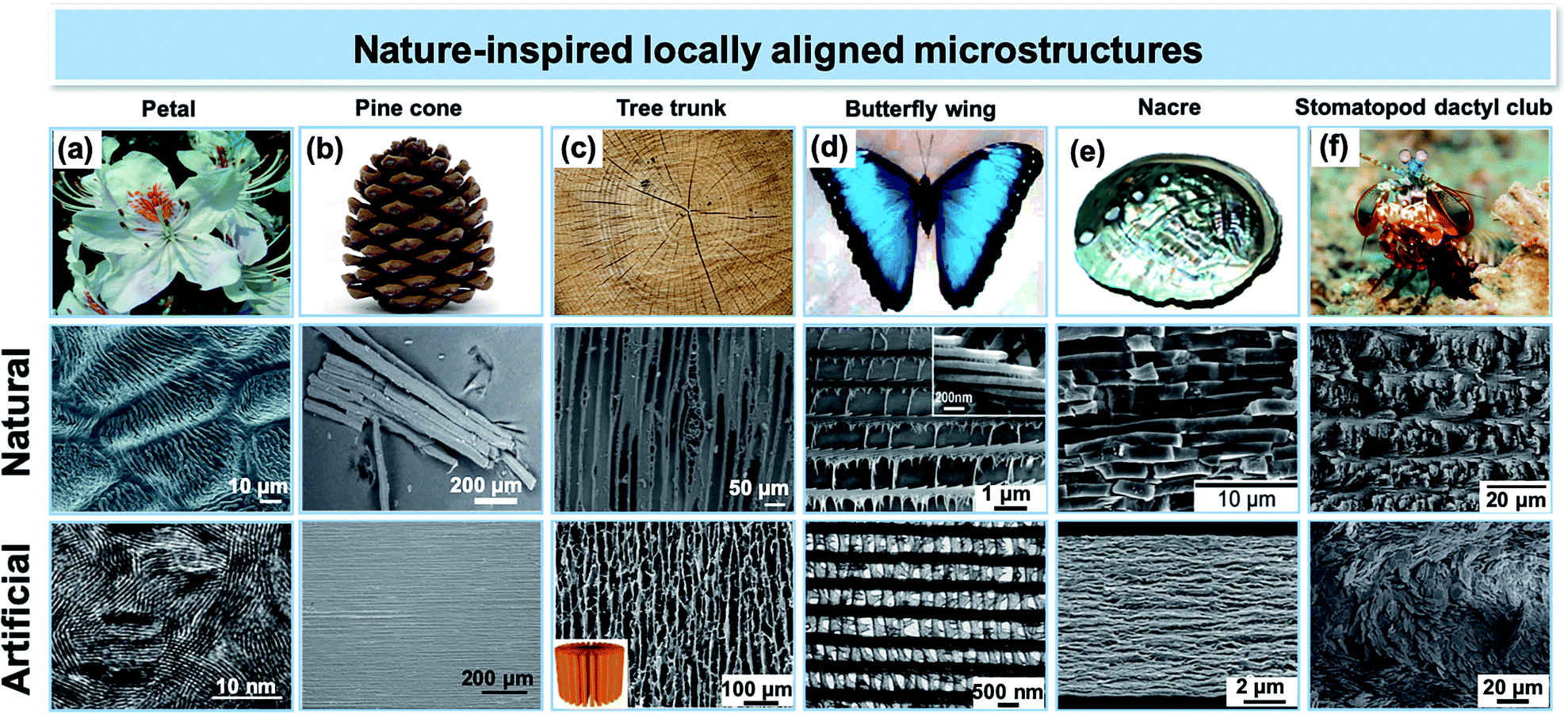
The diverse crystal structures and blooming functionalities in 2D nanomaterials provide great opportunities to establish optimized material performances for realistic device applications. Indeed, tailored microstructures with local orientation of 2D nanomaterials could be an efficient pathway to unlock their potential and transpose their outstanding nanoscopic properties to the macroscopic scale. Controlling the assembly of anisotropic particles into hierarchical structures is a way to induce new, unique macroscopic properties that cannot be obtained in random configurations. This effect is well demonstrated in natural materials, which have evolved complex microstructures with local alignment over the years, providing us with an inspirational gallery for structural design and fabrication.26–30 By mimicking these natural microstructures, many advanced artificial materials exhibiting attractive properties and functions have been realized (Fig. 1). We can imagine that if these delicate local orientations can be precisely controlled and reasonably combined with various 2D nanomaterial combinations, any set of desired functionalities could be realized.
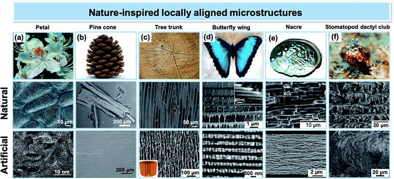 |
| | Fig. 1 Representative locally aligned microstructures found in natural species and their mimetic artificial counterparts: (a) locally ordered surface patterning of Yunnan rhododendron petals and MoS2 nanofilms with molecular layers perpendicular to the substrate. Reproduced from ref. 31 with permission from The Royal Society Publishing. Reproduced from ref. 32 with permission from the National Academy of Sciences. (b) Bi-layer active hygroscopic tissue of a Pinus coulteri pine cone and aligned carbon nanotubes (CNTs) in paraffin wax. Reproduced from ref. 33 with permission from The Royal Society Publishing. Reprinted with permission from ref. 34. Copyright (2015) American Chemical Society. (c) Radial alignment in a tree trunk and freeze-casted graphene oxide (GO) aerogel with a radial and centrosymmetric structure. Reproduced from ref. 35 with permission from NC State University. Reprinted with permission from ref. 36. Copyright (2018) American Chemical Society. (d) Lamellae microstructure of the scales of a Morpho peleides butterfly wing and replica made of alumina. Reprinted with permission from ref. 37. Copyright (2006) American Chemical Society. (e) Brick-and-mortar layered microstructure of the nacre layer in seashells and artificial nacre made of layered poly(vinyl alcohol)–clay–nanofibrillar cellulose. Reproduced from ref. 38 with permission from Elsevier. Reproduced from ref. 39 with permission from John Wiley and Sons. Reprinted with permission from ref. 40. Copyright (2014) American Chemical Society. (f) Helicoidal orientation in the stomatopod dactyl club and similar orientation pattern with alumina microplatelets. Reproduced from ref. 41 with permission from Elsevier. Reproduced from ref. 42 with permission from Springer Nature. | |
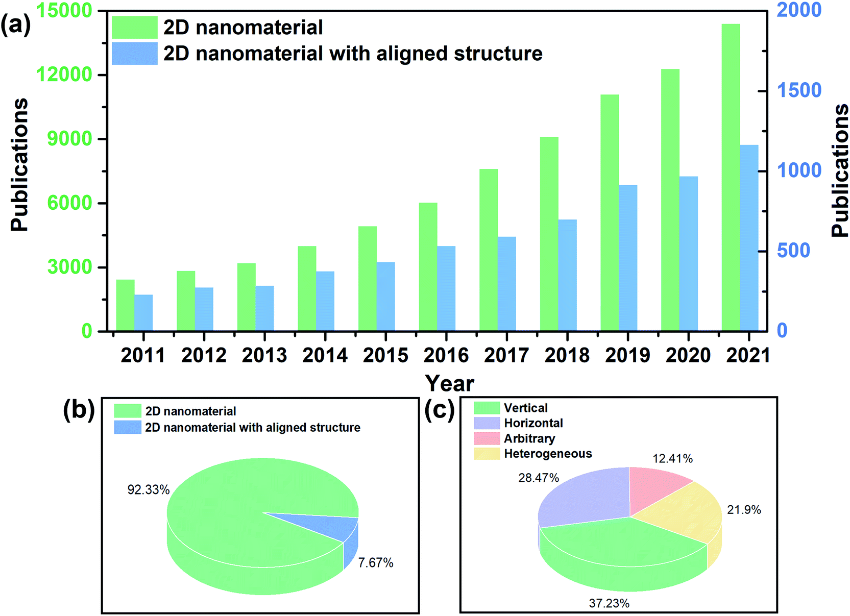
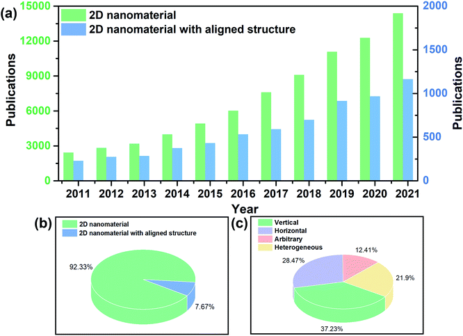
The capability of precisely controlling the alignment of 2D nanomaterials has always been exciting but rather challenging. Fig. 2a displays the statistical number of publications on 2D nanomaterials and 2D nanomaterials with an aligned structure from 2011 to 2021. In the past ten years, there has been a significant increase in 2D nanomaterial-related studies, reflecting the promise of 2D nanomaterials for materials development. The publications related to aligned 2D nanomaterials also exhibit a growing tendency especially in the latest years. However, these studies only comprise 7.67% of the total research on 2D nanomaterials (Fig. 2b), indicating an available, vacant area for further research. Classifying the alignment of 2D nanomaterials as vertical, horizontal, arbitrary and heterogeneous microstructures, it appears that vertical and horizontal alignment account for the most research interest (Fig. 2c).
 |
| | Fig. 2 (a and b) Publications on 2D nanomaterials and 2D nanomaterials with an aligned structure from 2011 to 2021. The publication numbers were collected from the Web of Science using the key words “2D nanomaterial” and “2D nanomaterial aligned structure” or “2D nanomaterial oriented structure” or “2D nanomaterial ordered structure”. (c) Publications on aligned 2D nanomaterials with different orientation types. | |
From these recent studies, one major observation is that the lateral size of 2D nanomaterials and their orientations greatly impact the properties at the microscopic and macroscopic scales. These results have already been reviewed and summarized by others. For example, Luo et al. compared the strategies of improving photocatalytic performances by assembling functional architectures with 2D nanomaterials and analyzed its role in enhancing the energy conversion efficiency.43 Zhang et al. reviewed the growth mechanism of vertically aligned graphene nanosheet arrays (VAGNAs) and discussed their properties for electrochemical energy applications.44 Yaraghi et al. focused on fabrication methods and structures of biomimetic structural materials with brick-and-mortar and helicoidal architectures.45 Cao et al. provided a survey on low-dimensional materials for electromagnetic (EM) applications and discussed the strategy of constructing well-aligned 2D nanosheets.46 Tan et al. stressed the advances of vertically aligned nanosheets (VANSs) for batteries.47 Furthermore, Huang et al. pointed out that aligned carbon-based electrodes (ACBEs) can greatly enhance the battery power density due to the combined advantages of an aligned structure and carbon-based materials.48 Shao et al. emphasized the role of the freeze casting technique in the formation of well-controlled biomimetic porous materials from low-dimensional building blocks.49 Moreover, Lei et al. reviewed the specific role of vertically aligned structures in polymer composite materials for multiple applications.50 Zhang et al. provided synthesis and modification methods of polymer composites with aligned 2D nanomaterials and their potential applications.51 In most of the reviews, the controlled orientation mainly focused on a single orientation type such as vertical or horizontal, throughout the bulk material, or limited fabrication methods for a specific target application. A systematic review on diverse orientation design of 2D nanomaterials and their augmented properties is thus still lacking.
In view of controlling the microstructural local alignment of 2D nanomaterials for improving performances, it is therefore timely to review the up-to-date development on this topic and to propose a vision on how to leverage the diversity in the chemistry and properties of 2D nanomaterials to yield multifunctional high-performance devices. Herein, we review the most recent research on controlled local orientation of 2D nanomaterials for functional designs and envision future prospects. The outline of this review is presented in Fig. 3. First, in this introduction, the background for studying 2D nanomaterials and the inspiration to develop locally aligned microstructures are provided. In the next section, we provide examples that demonstrate how oriented 2D nanomaterials can enhance the performances for selected applications, namely sensing, thermoelectrics and electrochemical energy harvesting, followed by reviewing the fabrication methods for horizontal, vertical, heterogeneous, and arbitrarily aligned microstructures. To bridge the gap between microstructural and 3D macroscopic devices, the fourth section of this review discusses how 3D printing can contribute to achieving locally aligned structures and what is its capability to build macroscopic architectures combining multiple chemistries. Finally, we anticipate the potential of controlled alignment of 2D nanomaterials for functional designs and applications and discuss remaining challenges, for the fabrication of next-generation smart multifunctional devices.
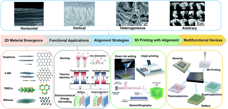 |
| | Fig. 3 Graphical outline of this review: from the background for emerging 2D nanomaterial study, established functional applications using oriented 2D nanomaterials, to fabrication methods of various orientations including 3D printing, following by the potential of developing multifunctional devices. Reprinted with permission from ref. 15. Copyright (2017) American Chemical Society. Reproduced from ref. 52 with permission from the Royal Society of Chemistry. Reproduced from ref. 53 with permission from Elsevier. Reproduced from ref. 54 with permission from John Wiley and Sons. Reprinted with permission from ref. 55. Copyright (2015) American Chemical Society. Reproduced from ref. 56 with permission from the Royal Society of Chemistry. Reproduced from ref. 57 with permission from Springer Nature. Reproduced from ref. 58 with permission from the Royal Society of Chemistry. Reproduced from ref. 59 with permission from John Wiley and Sons. Reproduced from ref. 60 with permission from Springer Nature. Reproduced from ref. 274 with permission from Springer Nature. Reproduced from ref. 323 with permission from the Royal Society of Chemistry. | |
2. Oriented 2D nanomaterials for functional applications
This section provides examples from the literature, which demonstrate why orienting 2D nanomaterials purposely is key for achieving high performance in macroscopic components. We specifically selected a few functional applications that we see as the most promising for future energy and sustainability enhancement and that are under intense research in the materials community. These are sensing, thermoelectrics and electrochemical energy harvesting applications. The reader is then invited to draw analogies for other applications of their interest, where aligned and specifically oriented 2D nanomaterials could enhance the properties and functionalities of materials and devices.
2.1 Sensing
A sensor is a signal generator that captures a physical input from its working environment and converts it into a readable output. An ideal sensor should possess high sensitivity, selectivity and stability.15,61,62 The sensitivity is typically determined by the ability of materials to respond to environmental stimuli such as optical, thermal, electrical, mechanical or chemical variations.63,64 2D nanomaterials, with their exceptional surface properties, are promising candidates for sensing applications. Controlling the alignment of 2D nanomaterials has proved to be beneficial in sensing mainly because it can improve (i) the density of exposed active sites, (ii) the surface-to-volume ratio, and (iii) the charge transfer within the oriented material.65 Gas sensing and photodetection are among the most extensively studied sensing applications using 2D nanomaterials. In gas sensing applications, the mechanism consists of transforming chemical potential into electrical current density through gas molecule adsorption, where the resistance change is closely related to chemical reactions occurring at the surface of the nanomaterials. For photodetection, the mechanism is to convert an incident optical signal into an electrical signal based on the optical responsivity of the material.66–70 Taking gas sensing as an example, the sensitivity (S) is defined as:| |  | (1) |
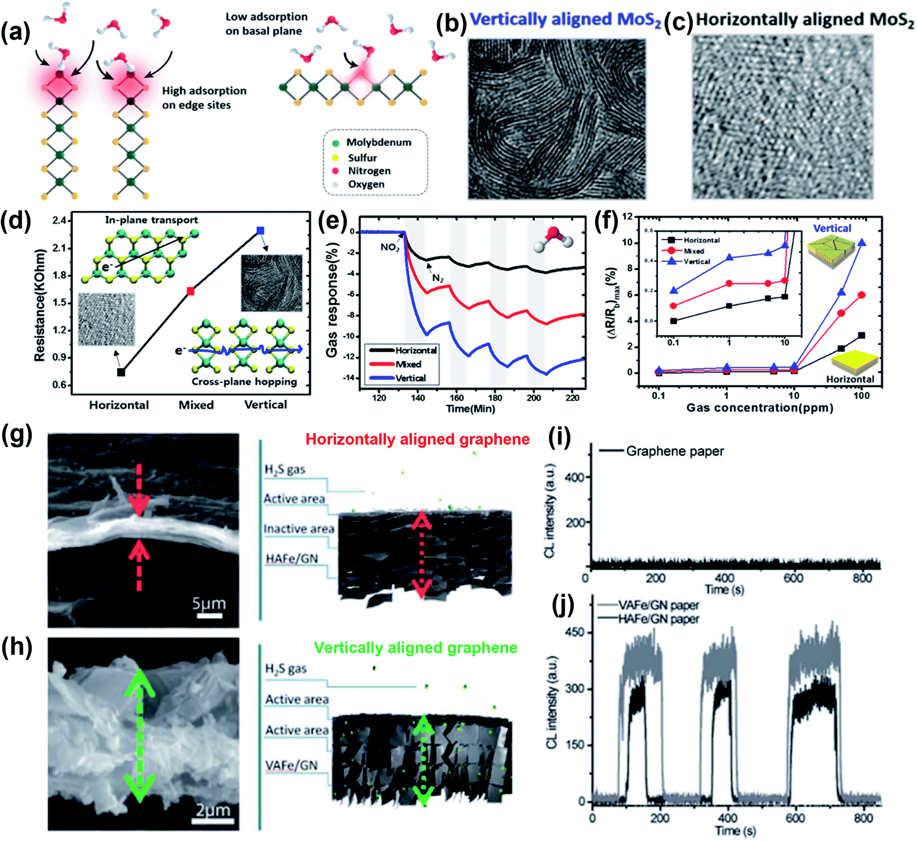
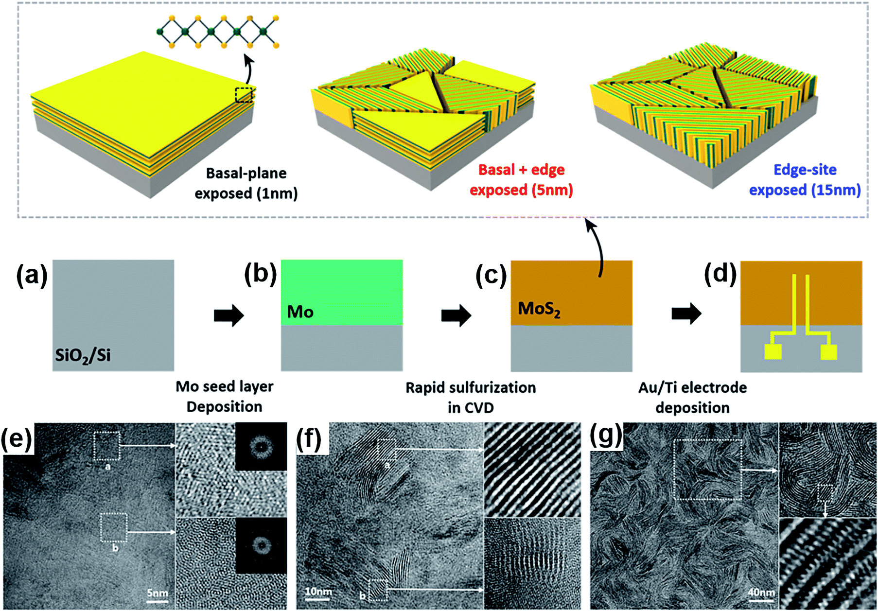
where ΔI is the gas-induced current change and I0 is the current of the sensor without gas.71–73 Various 2D nanomaterials such as MXenes,74,75 TMDCs,76–78 graphene79,80 and phosphorene81,82 have been used to absorb gases like NO2,77,83 CO,84 CO2,79,85 NH3,76,86 and H2S.87Fig. 4 illustrates the NO2 gas sensing properties of MoS2 films with horizontal, vertical and mixed alignment structures.55 During gas sensing, the gas adsorption capability is closely related to the binding energy between the active sites and the gas molecules. The exposed edge sites with high surface energy in vertically aligned MoS2 provided high adsorption, while the adsorption in the basal plane of horizontal alignment was much lower (Fig. 4a). Meanwhile, the resistance of the vertically aligned film was significantly increased, which was attributed to the dominated carrier transport within the van der Waals gaps in the cross-plane direction (Fig. 4d). As a result, the vertically aligned MoS2 film allowed a 5-times higher resistance variation (Fig. 4e) and could even detect 0.1 ppm of NO2 gas when the maximum amplitude of electrical responses (ΔR/Rb)max was 0.2%, which was impossible in the horizontally aligned film (Fig. 4f). In another example, Jiang et al. reported the H2S gas sensing response of Fe2O3/graphene nanosheets with horizontal and vertical alignments (Fig. 4g and h).87 The alignment was induced by controlled magnetic field assembly under a directed flow and will be described in Section 3 of this review. The vertically aligned Fe2O3/graphene nanosheets exhibited higher sensitivity (∼450 absorption units to 15 ppm H2S) than the horizontally aligned ones (∼350 absorption units to 23 ppm H2S) at a working temperature of 190 °C (Fig. 4j). This improved sensing capability in response to H2S gas could be contributed by a larger contact area as well as less resistance to the target gas flow. Islam et al. also observed high sensitivity to NO2 gas in vertically aligned MoS2 layers.72 The sensitivity was about 160–380% within a gas concentration range of 5–30 ppm, demonstrating a much higher response compared with the horizontally aligned layers. The higher sensitivity in the vertical alignment could be attributed to the exposed edge sites with sufficient dangling bonds, leading to high chemical reactivity and adsorption capability. These few, selected examples illustrate how the orientation of 2D nanomaterials can be utilized to boost the performance of sensing devices.
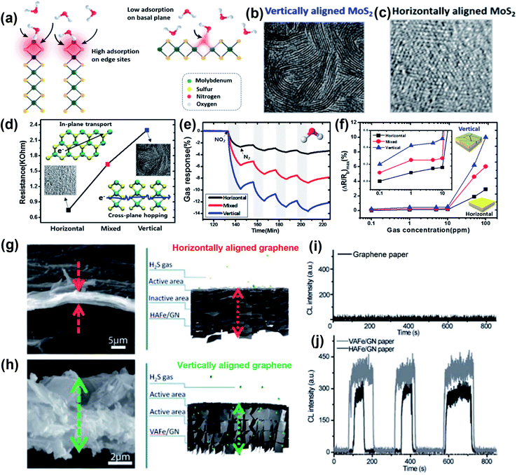 |
| | Fig. 4 Gas adsorption properties of MoS2 films with horizontal, vertical and mixed alignments for gas sensing. (a) Schematic illustration showing the mechanism of gas adsorption on the edge sites and basal plane of MoS2 films. SEM images of (b) vertically aligned and (c) horizontally aligned MoS2 films. (d) Resistance in relation to different alignments with higher resistance in the vertically aligned MoS2 film because of cross-plane hopping of carriers. (e) Resistance changes of 100 ppm NO2 gas adsorption demonstrating the superior gas sensing properties of edge sites than the basal plane. (f) Maximum electrical responses of the synthesized MoS2 films within 0.1–100 ppm of NO2 exposure. Reprinted with permission from ref. 55. Copyright (2015) American Chemical Society. Morphologies of (g) horizontally aligned Fe2O3/graphene paper and (h) vertically aligned Fe2O3/graphene paper. Response curves of H2S on the chemiluminescence (CL) intensity of (i) graphene paper fabricated by traditional filtration and (j) vertically arranged Fe2O3/graphene nanosheets (VAFe/GN) and horizontally arranged Fe2O3/graphene nanosheets (HAFe/GN) with a controlled orientation. Reproduced from ref. 87 with permission from the Royal Society of Chemistry. | |
2.2 Thermoelectrics
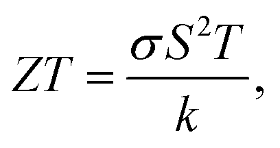
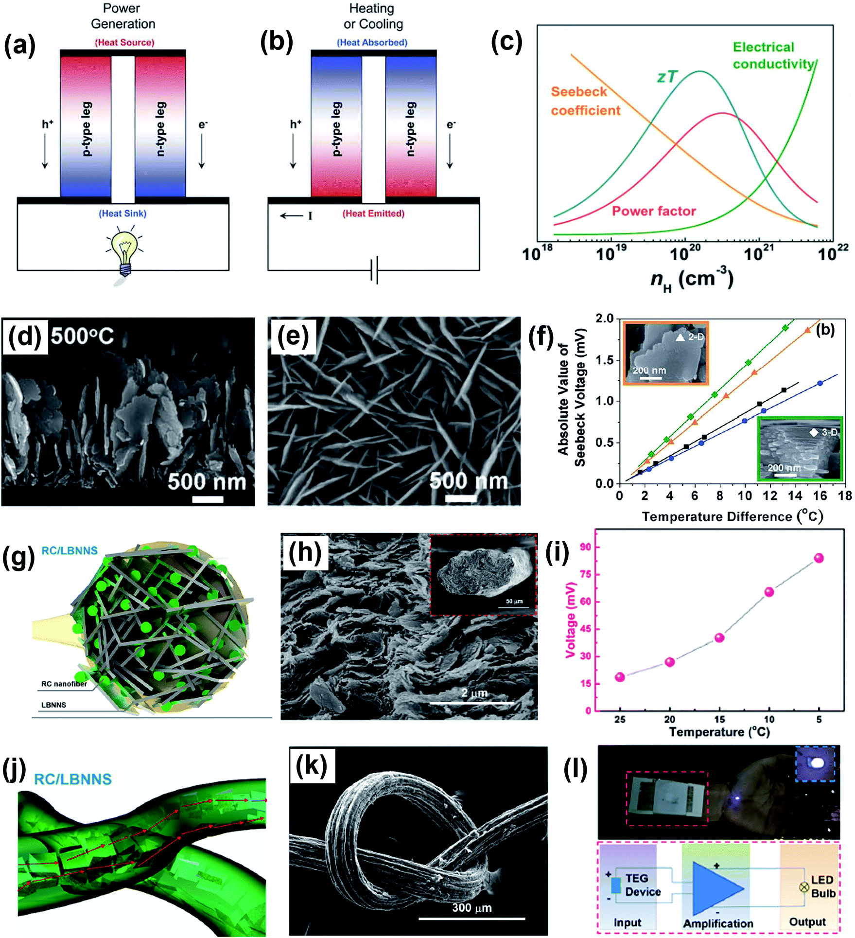
To tackle the increasing global energy demand, the ability of harvesting electrical energy from waste heat from the thermoelectric effect has attracted considerable attention.88–91 The thermoelectric effect refers to the phenomenon by which a temperature difference is directly converted into an electric voltage and vice versa. The process of voltage generation from a temperature difference is known as the Seebeck effect (Fig. 5a), while the conversion process of creating a temperature difference upon an applied voltage is the Peltier effect (Fig. 5b).92 The working mechanism of the thermoelectric effect is related to the perturbation of charge carriers in equilibrium distribution. When there is a temperature gradient, the charge carriers migrate from high temperature to low temperature, leading to the generation of voltage. The performance of thermoelectric materials is characterized by the dimensionless thermoelectric figure of merit, ZT:| |  | (2) |
where σ is the electrical conductivity, S is the Seebeck coefficient, T is the temperature, and k is the thermal conductivity.93 Based on eqn (2), an ideal thermoelectric material should possess a high electrical conductivity, a high Seebeck coefficient and a low thermal conductivity. The optimum carrier concentration for a high thermoelectric performance and thermoelectric power factor (σS2) is illustrated in Fig. 5c.
 |
| | Fig. 5 Controlled alignment of 2D materials for thermoelectric applications. Schematic illustration of thermoelectric devices for (a) voltage generation and (b) heating or cooling applications. Reproduced from ref. 56 with permission from the Royal Society of Chemistry. (c) Optimum carrier concentration (nH) for the thermoelectric figure of merit (ZT) and power factor. Reproduced from ref. 104 with permission from John Wiley and Sons. Well-aligned 2D Bi2Te3 nanoflakes as thermoelectric materials. SEM images of (d) cross sectional and (e) top view morphologies. (f) Seebeck voltage as a function of the temperature difference in aligned 2D and 3D Bi2Te3 nanoblocks. Reproduced from ref. 101 with permission from the Royal Society of Chemistry. Aligned regenerated cellulose (RC)/BNNS composite filaments for wearable thermoelectric devices. (g and j) Schematic representation of RC/BNNS composite filaments. (h and k) Morphology of RC/LBNNS composite filaments. (i) Generated voltage at different ambient temperatures. The red arrow refers to the heat conduction direction. (l) Diagram of a wearable thermoelectric device and its ability to light a LED bulb. Reproduced from ref. 103 with permission from Elsevier. | |
Besides the well-known thermoelectric materials like Bi2Te3, Sb2Te3, PbTe, etc., emerging 2D nanomaterials with a high electrical conductivity or high Seebeck coefficient, such as graphene,94–96 TMDCs,97,98 and MXenes,99,100 are also promising for thermoelectric applications. Interestingly, controlling the alignment of 2D nanomaterials is a great way to enhance the thermoelectric performances. The pivotal concepts of this enhancement are to (i) increase ion mobility in aligned carrier pathways for improved electrical conduction, and (ii) induce more phonon scattering to suppress thermal conduction or tune the thermal conductivity along the selected directions. For example, Chang et al. investigated the role of alignment in 2D Bi2Te3 nanosheets for thermoelectric applications.101 2D Bi2Te3 nanosheets with a vertical alignment to the SiO2/Si substrate were grown by pulsed laser deposition at 500 °C (Fig. 5d and e). The good alignment contributed to improved electrical conductivity and Seebeck voltage generation compared to randomly aligned nanosheets (Fig. 5f). Consequently, an in-plane thermoelectric power factor of 1.35 μW cm−1 K−2 was obtained in vertically aligned nanostructures, which was effectively improved compared to that under random conditions (<1 μW cm−1 K−2). In another example, Oh et al. achieved significantly improved thermoelectric properties in an aligned MoS2/graphene nanoribbon heterojunction.102 A vertical heterojunction was designed to maximize the carrier transport: carriers can pass back and forth between the graphene and MoS2 nanosheets easily to induce the thermoelectric effect. The as-synthesized nanostructure exhibited an enhanced electrical conductivity of 700 S m−1 and a high power factor of 222 μW m−1 K−2. In addition, Wu et al. developed regenerated cellulose (RC)/BNNS composite filaments with an oriented microstructure using a wet-spinning procedure, which will be described later in the review.103 With the alignment, the large-sized BNNSs were confined among adjacent RC nanofibers at a high filler loading, providing high anisotropy to the filaments (Fig. 5g, h and j, k). The aligned RC/BNNS composites displayed extraordinary thermal conduction and could be used in wearable thermoelectric generator (TEG) devices that can promptly transport body heat from skin to the surface of the composites. A maximum Seebeck voltage of 84 mV was achieved at an ambient temperature of 5 °C (Fig. 5i). Therefore, the aligned composites can be utilized as a wearable heat spreader to improve energy harvesting efficiency, which demonstrates potential in high-performance wearable electronics (Fig. 5l). These exciting examples demonstrate how the orientation of 2D nanomaterials can be leveraged to increase the functionalities of thermoelectric devices for robotics, energy harvesting, and electronics, among others.
2.3 Electrochemical energy harvesting
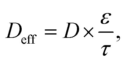
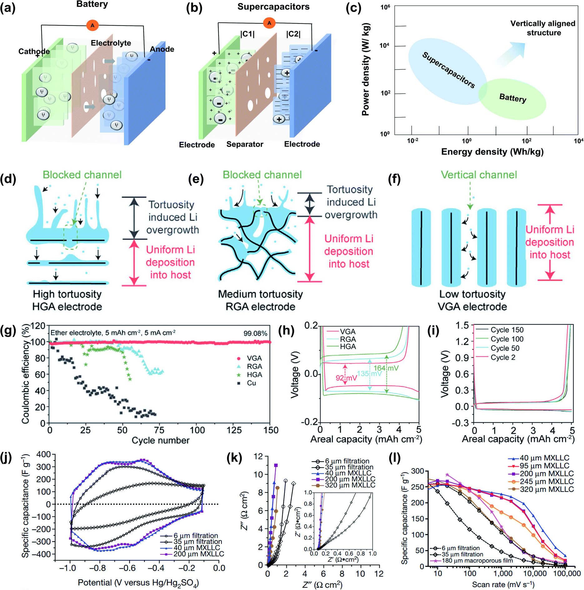
An ideal electrochemical energy storage (EES) device should have low cost, long life span, high energy and power density, good recycling stability, and safety. Two main types of EES devices are batteries and supercapacitors that are composed of two porous electrodes separated by a porous layer, the electrolyte. During charging and discharging, ions, such as lithium, travel back and forth between the cathode and the anode through the electrolyte (Fig. 6a). In supercapacitors, the energy storage is attributed to a double layer capacitance and a surface redox reaction creating pseudocapacitance, as described in Fig. 6b. Since the discovery of graphene, 2D nanomaterials have become predominant electrode materials in pursuit of high power and energy density for batteries and supercapacitors.105–107 For example, MXenes have a conductive inner transition metal carbide layer that allows fast electron supply to active sites. Meanwhile, a transition metal oxide-like surface is redox active, and the 2D morphology and nanoconfined fluid molecules enable fast ion transport.108–110 The MXene electrode structure in supercapacitors is able to deliver up to 210 F g−1 at a scan rate of 10 V s−1 and a volumetric capacitance of ∼1500 F cm−3.111 However, 2D nanomaterials used as electrodes tend to aggregate and restack into microparticles, which result in low electrolyte ionic conductivity and high electrode tortuosity and further limit ion transport between the electrode and the electrolyte. The ion transport in electrolytes includes ion migration and ion diffusion. It is related to the intrinsic conductivity of ions and the tortuosity of the porous electrode. The effective diffusivity in the electrolyte is commonly defined as:| |  | (3) |
where D is the diffusion coefficient, ε is the porosity, and τ is the tortuosity. An empirical correlation between ε and τ is provided by a Bruggeman-type relationship:where α is the Bruggeman exponent correlated with the porosity, and γ is a scaling factor.112 When the conductive pathways are composed of straight channels that are parallel to the transport direction, τ is 1.113 A lower value of tortuosity leads to higher effective ionic diffusivity and ionic conductivity. Therefore, to facilitate ion transport in 2D nanomaterial-based electrodes, designing vertically aligned microstructures is a promising strategy to enhance power and energy density (Fig. 6c).113 Numerous examples in the literature illustrate the benefits of this strategy in batteries and supercapacitors.114,115 The most recent progress in this domain is reviewed in the following paragraph.
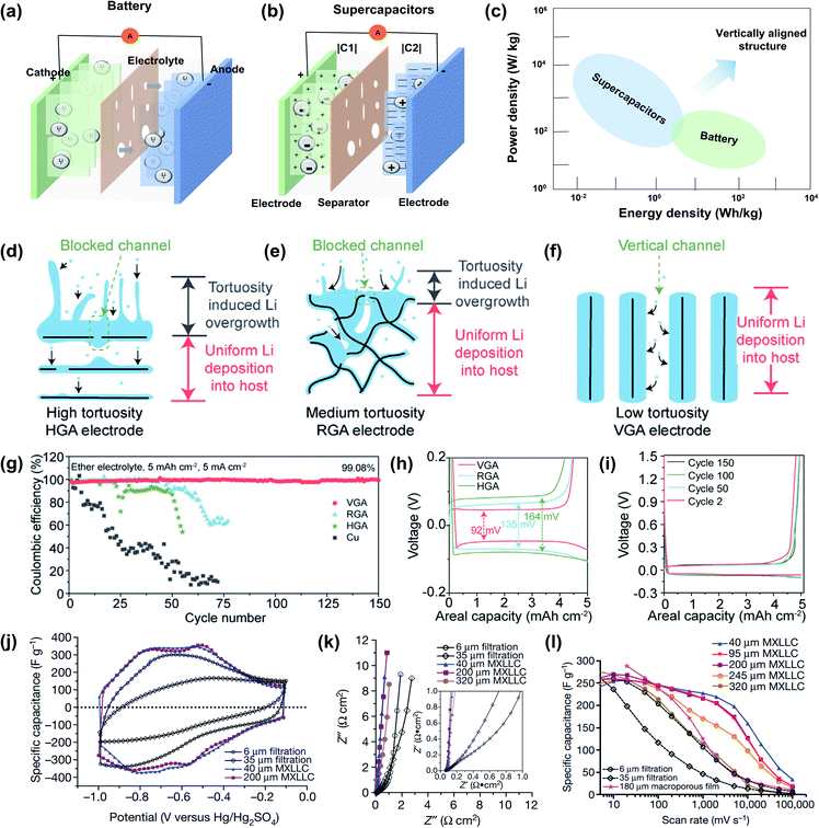 |
| | Fig. 6 Schematic illustration of (a) batteries and (b) supercapacitors. C1 and C2 refer to the capacity of the cathode and anode. (c) The Ragone plot of batteries and supercapacitors, in which the vertically aligned structure promotes the enhancement of power and energy density. Li-deposition behavior in the structure of the (d) horizontally aligned electrode (HGA), (e) randomly arranged electrode (RGA), and (f) vertically aligned electrode (VGA). Electrochemical performance of the reduced graphene oxide anodes with (g) Li cycling coulombic efficiency (CE) on different anodes with an ether electrolyte at a current density of 5 mA cm−2 and a capacity of 5 mA h cm−2. (h) Corresponding voltage-versus-capacity plot of different electrodes in the first cycle. (i) Voltage-versus-capacity plot of the VGA electrode during different cycles. Reproduced from ref. 123 with permission from Elsevier. Electrochemical performance of vacuum-filtered MXene papers and MXLLC films with (j) cyclic voltammograms at a scan rate of 100 mV s−1. (k) Nyquist plots for different MXene films with real impedance Z′ and imaginary impedance Z′′. (l) Rate performance of vacuum-filtered MXene papers and MXLLC films at scan rates ranging from 10 to 100![[thin space (1/6-em)]](https://www.rsc.org/images/entities/char_2009.gif) 000 mV s−1. Reproduced from ref. 116 with permission from Springer Nature. 000 mV s−1. Reproduced from ref. 116 with permission from Springer Nature. | |
Vertically aligned structures composed of 2D nanomaterials including graphite, graphene, lithium metal phosphate, MXenes, and transition metal oxides have exhibited outstanding performances and promising commercialization prospects for batteries and supercapacitors. Indeed, vertical alignment of 2D nanosheets enables directional ion transport that can lead to thickness-independent electrochemical performances in thick films.116–119 A recent study demonstrated successful alignment of graphite with superparamagnetic nanoparticles of Fe3O4 driven by a magnetic field, which allows cycling at a fast rate of up to 2C with a specific charge three times higher than that of the anode with a disordered structure.120 The out-of-plane tortuosity of graphite aligned perpendicularly to the current collector is reduced by nearly four times. In addition to graphite, graphene has attracted much more attention because of its excellent electrical conductivity and ultrahigh surface area. Described by Hao et al., three structures of graphene including vertically (VGA), horizontally (HGA), and randomly (RGA) aligned electrodes were fabricated, which showed a tortuosity of 1.25, 4.46, and 1.76, respectively.121 High electrode tortuosity induced locally higher current density on the top surface of horizontal alignment and random graphene, which resulted in dendritic Li overgrowth on the surface (Fig. 6d and e). In contrast, lower electrode tortuosity in the vertically aligned graphene enabled homogeneous Li transport and uniform Li deposition across vertically aligned graphene (Fig. 6f).121 Upon cycling Li on the different anodes as shown in Fig. 6g, the HGA electrode showed a decay of the coulombic efficiency (CE) to 90% after 24 cycles, whereas the CE of the RGA electrode decreased to 90% after 48 cycles. In turn, the VGA electrode held a stable CE of ∼99.08% after 150 cycles. In the voltage–capacity test, VGA presented a lower overpotential (46 mV) than RGA (67.5 mV) and HGA (82 mV) (Fig. 6h), and held a stable overpotential of ∼46 mV even after 150 cycles (Fig. 6i).121 In another example, an electrode with vertically aligned Fe3O4/GO exhibited an energy density of 724 mA h g−1 at 2 A g−1, which was much higher than that with the horizontal alignment.122 Beyond graphene, MXenes also have a large potential for enhanced supercapacitors. Vertically aligned MXenes allow ion transport directly inside the electrode, which results in thickness-independent electrochemical performances. An example of vertically aligned titanium carbide (Ti3C2Tx, MXLLC) was achieved by mechanical shearing.116 The vertically aligned MXLLC exhibited much higher cyclic voltammogram performances than the horizontally aligned film. Furthermore, the Nyquist plots of MXLLC electrodes were nearly vertical at all frequencies, indicating that fast ion diffusion was critical for the independence from the thickness (Fig. 6k). In addition, the rate performance of the MXLLC films declined negligibly when the film thickness was increased from 40 μm to 200 μm (Fig. 6l). Some studies on vertically aligned structures in electrodes for EES are collected in Table 1, which demonstrate the better performance of vertical over horizontally oriented electrodes. These selected examples illustrate how controlling the orientation of 2D nanomaterials enhances the performance of batteries and supercapacitors.
Table 1 The electrochemical performance of batteries and supercapacitors produced with vertically aligned 2D nanomaterials as the electrode. The electrode material, the orientation method and the electrode thickness are also featured in the table. The orientation methods are explained in Section 3 of this review
| Electrode |
Orientation method |
Electrode thickness |
Cycling stability |
Energy power & density |
Ref. |
| 3D aligned Fe3O4/GO |
Freeze-casting |
∼600 μm |
— |
724 mA h g−1 @ 2 A g−1 |
122
|
| Traditional slurry-casting method |
— |
162 mA h g−1 @ 2 A g−1 |
| LiFe0.7Mn0.3PO4 nanoplates/graphene |
Freeze-casting |
— |
85.6% (450 cycles) |
122.3 mA h g−1 @ 2C |
124
|
| Traditional slurry-casting method |
— |
67% (450 cycles) |
68.7 mA h g−1 @ 2C |
| Graphite/sodium carboxymethyl cellulose |
Freeze-casting |
575–800 μm |
— |
∼18, ∼14, and ∼7 mA h cm−2 @ 0.1C, 0.2C, and 1C |
125
|
| VOPO4 nanosheet |
Freeze-casting |
800 μm |
83% (500 cycles) |
144 mA h g−1 @ 0.2C |
126
|
| Drop-casting |
— |
122 mA h g−1 @ 0.2C |
| Graphite |
Magnetically aligned casting |
— |
— |
83 mA h g−1 @ 2C |
120
|
| No alignment |
— |
— |
23 mA h g−1 @ 2C |
| Ti3C2Tx/graphite |
Magnetically aligned casting |
— |
90% (5000 cycles) |
60 mA h g−1 @ 2 A g−1 |
127
|
| No alignment |
— |
77% (5000 cycles) |
16.7 mA h g−1 @ 2 A g−1 |
| Ti3C2Tx |
Freeze-casting |
700 μm |
97.7% (14000 cycles) |
150 kW kg−1 @ 1000 A g−1 |
128
|
| MXLLC |
Shear induced alignment |
40–200 μm |
100% (20000 cycles) |
220–207 F g−1 @ 2000 mV s−1 |
116
|
| Vacuum-filtered film |
6–35 μm |
— |
33–77 F g−1 @ 2000 mV s−1 |
We have seen that controlling the orientation of 2D nanomaterials can enhance the properties and functionalities of sensing and thermoelectric devices, as well as batteries and supercapacitors. These few devices are playing a major role in the development of greener energies, to detect polluting elements or generate energy. The key fundamental reason for the enhancement of the functionalities arises from the conjunction of the outstanding intrinsic properties of 2D nanomaterials with their orientation in a specific direction at the microscopic scale. Even though these various examples are exciting, a number of challenges remain for transposing these properties and enhanced functionalities into real, macroscopic devices, such as scale-up, locally controlled orientation and shaping, which are discussed here. To address these challenges in manufacturing, a number of versatile methods have been systematically investigated, which are reviewed in the following section.
3. Processing techniques for controlled alignment
The desired local orientation direction and global microstructure of a material are determined by what the application demands. Over the recent years, diverse techniques have been established to achieve specific orientations of 2D nanomaterials. We classify these orientation types into horizontal, vertical, heterogeneous, and arbitrary structures. Overall, some methods lead to one of these orientation types, whereas others can produce several, which is the case for example of magnetically assisted orientation and chemical vapor deposition (CVD). The methods that can achieve versatile orientations by tailoring the fabrication parameters will be discussed as arbitrary structural alignment processes. In this section, we give an overview of the most representative processing methods to achieve the four alignment types mentioned earlier using 2D nanomaterials. The advances of different alignment techniques, pivotal control parameters and typical aligned structures are discussed.
3.1 Horizontal microstructures
A material with good horizontal orientation of 2D nanomaterials shows typically exfoliated, dispersed nanosheets that are stacked in a highly ordered aligned structure. In turn, this alignment allows a higher concentration of nanosheets and highly compact assembly. Thanks to this horizontal orientation, the anisotropic nanoscopic properties of the 2D nanomaterial can be transferred to the larger structure. For example, the anisotropic orientation can strengthen the macroscopic material along the aligned direction, while the properties in the perpendicular direction are not affected.129 The techniques to obtain horizontally aligned structures typically are vacuum-assisted filtration, tape casting, wet spinning, centrifugal casting, direct bottom-up synthesis, hot pressing and self-assembly, and are summarized in Table 2. The mechanisms, characteristics and advantages of these techniques are systematically introduced in this section.
Table 2 Processing techniques for horizontal alignment of 2D nanomaterials
| Method |
Alignment principle |
Achieved structure |
Advantages |
Limitations |
Ref. |
| Vacuum-assisted filtration |
Vacuum filtration of colloidal solution to compress the 2D nanosheets horizontally |
Film, highly ordered, free-standing layered structure |
Wide material selection, inexpensive, simple setup |
Time-consuming process, requires low viscosity in colloidal solution |
129–134, 146, 172 and 173 |
| Tape casting |
Application of horizontal shear force on a viscous solution using a doctor blade |
Film, highly ordered, layered structure |
Scalable, industrially adaptable |
Slow processing |
137, 138, 174 and 175 |
| Wet spinning |
Extrusion and spinning of a self-assembled colloidal dispersion through a spinneret in a solution bath |
Fiber, layered structure |
Industrially adaptable, no thermal degradation |
Slow processing, requires volatile organic solvents |
139, 140, 142 and 176 |
| Centrifugal casting |
Casting of a 2D nanosheet dispersion on the inner surface of a rotating hollow tube to align them using centrifugal force |
Film, highly aligned, compact layered structure |
Wide material diversity, high efficiency, scalable synthesis |
Requires specific equipment, with an appropriate inside diameter for efficient centrifugation |
57, 144 and 145 |
| Hydrothermal |
Heating of an aqueous or organic medium above the boiling point to induce pressure rise and chemical reaction |
Nanosheets/film, well-defined aligned layers |
High quality nanocrystals, high yield, low cost |
Requires specific autoclaves, safety issue during the reaction |
153–155
|
| Gelation |
Nanosheet hydrogel growth at a solid–liquid interface by an electrochemical reaction |
Film, porous layered structure |
Simple setup, scalable, controllability of gel structures |
Porous morphology, time-consuming process |
151 and 156–158 |
| Hot-pressing |
Densification process using uniaxial pressure and temperature to simultaneously align and sinter |
Film/bulk, closely packed structure |
Compact microstructure, improved mechanical properties |
Requires specific equipment and operation, limited efficiency |
159, 163, 164 and 177 |
| Langmuir–Blodgett (LB) assembly |
Spreading of 2D nanosheets at a liquid–air interface which align due to capillary forces |
Thin monolayer films |
Simple operation, accurate thickness control |
Limited resistivity to high temperature, slow deposition |
168, 169, 171, 178 and 179 |
3.1.1 Vacuum-assisted filtration.
Vacuum-assisted filtration (VAF) or vacuum-assisted self-assembly (VASA) is a flexible technique to synthesise well-ordered and free-standing films or papers.129 It is one of the simplest and most commonly used methods to achieve horizontal alignment for a wide variety of 2D nanomaterials. Fig. 7a1 illustrates the fabrication process using VAF of a film with horizontally ordered layers, starting from a liquid solution containing dispersed nanosheets. This method utilizes a vacuum-generated flow to filter the nanosheets from an aqueous or organic dispersion over a filtration membrane. In addition, to obtain a homogeneous dispersion in the final layered nanosheets and increase their mechanical properties, a hydrophilic or hydrophobic polymer can be added into the dispersion.129–131 The mechanism of horizontal alignment via VAF is explained by the densification process during solvent removal. In a typical vacuum filtration process, when the solvent is gradually removed, the well-dispersed nanosheets are brought into close contact, leading to the formation of semi-ordered loose aggregates. As the top loose aggregates are exposed to the air–solvent interface, the compression force brings the nanosheets to the perpendicular direction of the flow. The gaps between nanosheets close, resulting in the formation of a compact film.130 In the end, assisted by VAF, the disordered nanosheets in solution are sequentially aligned parallel to the air–solvent interface (Fig. 7a2–a4). For example, Lin et al. synthesized highly aligned graphene oxide (GO) papers by using VAF.132 Thanks to the ultralarge GO nanosheets (average area of 272.2 μm2) with compact stacking and well-aligned microstructures, the GO paper achieved more than 3-fold improvement in electrical conductivity and enhanced mechanical properties including Young's modulus by 320% and tensile strength by 280%. Similarly, Ling et al. reported flexible and free-standing Ti3C2Tx MXene films fabricated by VAF.133 By tailoring the MXene content in solution, the obtained film thickness can be easily controlled. The as-fabricated Ti3C2Tx films could be used as electrodes in supercapacitors because of the rapid cation intercalation between the well-aligned layers. Moreover, Ding et al. manufactured membranes with a horizontally oriented MXene using VAF.134 Owing to the regular sub-nanometer spacing between aligned MXene layers, the membrane provided fast and precise molecular sieving channels for gas separation with H2 permeability higher than 2200 Barrer and H2/CO2 selectivity higher than 160. Although the VAF method has multiple advantages such as unlimited material selection, a simple setup and facile control of film thickness, it also has limitations from the time-consuming procedure and prerequisite of low viscosity for efficient filtration, especially when a polymer is involved.
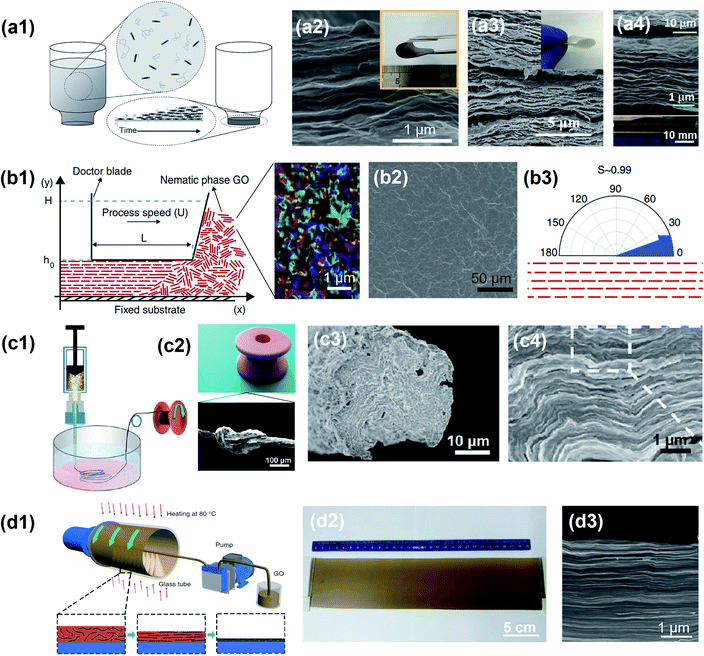 |
| | Fig. 7 Horizontal alignment of 2D materials assisted by mechanical force. (a1) Schematic representation of the vacuum-assisted filtration of nano-composite films. Reproduced from ref. 129 with permission from John Wiley and Sons. (a2) SEM image showing the cross section of the horizontally aligned MXene membrane. Reproduced from ref. 134 with permission from Springer Nature. (a3) SEM image of an aramid nanofiber (ANF)/BNNS film with a tightly packed microstructure. Reproduced from ref. 146 with permission from John Wiley and Sons. (a4) Cross-sectional SEM images of flexible free-standing Ti3C2Tx/PDDA films. Reproduced from ref. 133 with permission from the National Academy of Sciences. (b1) Schematic of tape casting processing of nematic graphene oxide (GO). (b2) SEM image showing the top surface of the shear-aligned GO membrane. (b3) Organization of graphene sheets in membranes. Reproduced from ref. 137 with permission from Springer Nature. (c1) Schematic representation of wet spinning for polyacrylonitrile-grafted GO (GO-g-PAN) fibers and (c2) fabricated GO-g-PAN fibers. (c3 and c4) Cross-sectional SEM images of GO-g-PAN3 fibers with horizontally aligned layers. Reprinted with permission from ref. 139. Copyright (2013) American Chemical Society. (d1) Schematic of the continuous centrifugal casting process. (d2) A GO film with a dimension of ∼30 × 10 cm2 and a thickness of ∼100 μm. (d3) SEM image of a GO film showing a highly aligned and compact layered structure. Reproduced from ref. 57 with permission from Springer Nature. | |
3.1.2 Tape casting.
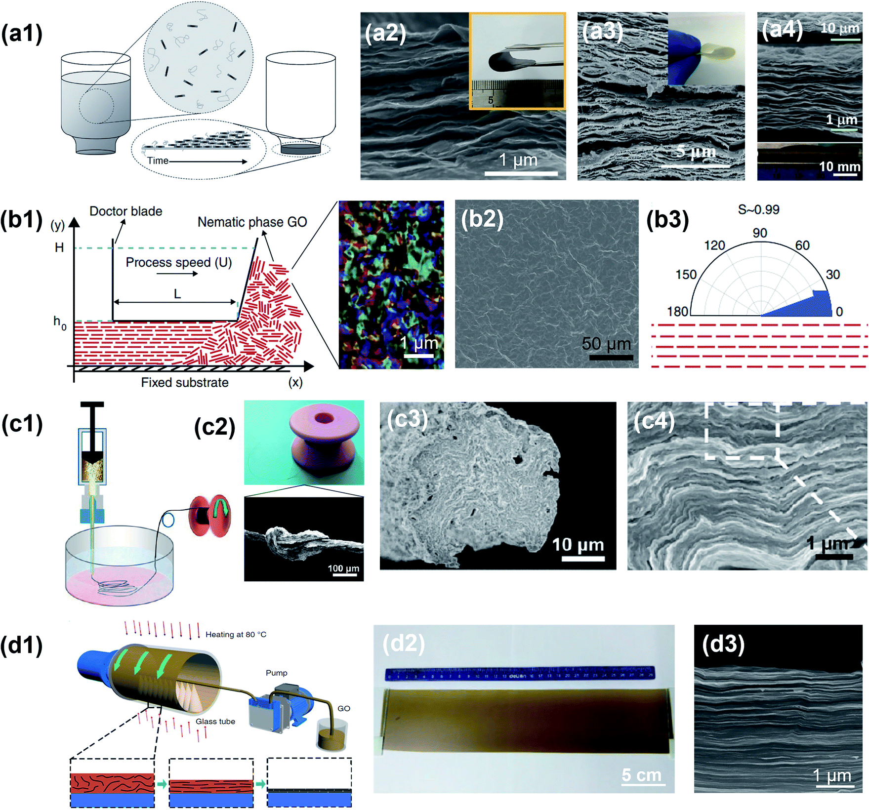
Tape casting, doctor blading or knife coating, is a well-established method to induce shear-induced alignment and to fabricate thin membranes from a viscous slurry.135,136 The membrane thickness can vary from 0.01 to several millimeters and can be controlled by setting the distance between the doctor blade and the substrate. More importantly, the membrane's lateral dimension is only limited by the shear apparatus, allowing its utilization in commercial production. In a typical slurry preparation, 2D nanosheets or ceramic precursors are mixed with a solvent, dispersant, binder and plasticizer at a ratio optimized for homogeneity and shear-thinning properties. The procedure is to use a doctor blade to spread out the slurry over a flat substrate (Fig. 7b1).137,138 Due to the shear generated by the motion of the doctor blade, the initial random orientation of the 2D nanosheets in slurry is overcome and well-aligned layers are formed.138 For example, Akbari et al. introduced tape casting as a scale-up method to fabricate highly ordered graphene-based membranes.137 The top surface morphologies of the film showed good uniformity and continuity (Fig. 7b2). They further investigated the extent of local orientation as the in-plane stacking order in the membranes using polarized light imaging, where a scalar parameter, S, was used to quantify the alignment extent (Fig. 7b3). This scalar parameter is defined as:| |  | (5) |
where θ is the angle between the mean azimuth and each pixel. When S = 1, the alignment is perfectly oriented in parallel, while S = 0 represents a completely random alignment. As a result, the shear-aligned membrane exhibited S values of about 0.99. Their results indicate the potential of tape casting to obtain aligned 2D nanomaterials.
3.1.3 Wet spinning.
Wet spinning is a mature technology that is industrially viable. It is a solution spinning process, where a thermoplastic polymer is dissolved in a solvent and extruded through a spinneret to form fibers that consolidate as the solvent evaporates. When it comes to 2D nanomaterials, this technique has been utilized to fabricate fibers which contain layer-stacked nanosheets. In a typical synthesis procedure, the nanosheets are well-dispersed in an organic solvent. Then, the macroscopic assembly of fibers is conducted by continuously spinning into the coagulation bath via a spinneret (Fig. 7c1 and c2).139 When the dispersion passes through the spinneret, a unidirectional flow is generated that assembles the nanosheets horizontally along the fiber direction. The as-fabricated fibers exhibit a dense and layered microstructure containing nanosheets and polymers, which recalls the brick-and-mortar fashion found in natural nacre (Fig. 7c3 and c4). Moreover, it should be noted that the successful alignment of nanosheets is closely related to their liquid crystal self-assembly in the initial colloidal dispersion. The formation of nematic and lamellar liquid crystals with nanosheet colloids is critical in achieving desired alignment, where the material concentration, size and dispersion should be properly controlled.140–142
3.1.4 Centrifugal casting.
Compared with the previous mechanical force-assisted methods, centrifugal casting is a time efficient method to assemble 2D nanomaterials into highly aligned and compact films.57,143 For example, it can complete the synthesis of 10 μm-thick graphene oxide films within 1 minute, which provides the possibility of fast processing for industries.57 Moreover, centrifugal casting is scalable and can produce continuous films up to the meter scale. Fig. 7d1 presents the schematic of the continuous centrifugal casting process of GO nanosheets. In a typical process, the nanosheets are dispersed in solution, which continuously deposits on the inner surface of a hollow tube rotating at speeds up to 2500 rpm. A temperature of about 80 °C can be applied simultaneously to accelerate the solvent evaporation. After reaching the desired thickness and complete water removal, a homogeneous GO film is obtained (Fig. 7d2). Due to the high-speed rotation of the hollow tube, a strong centrifugal force is induced along the radial direction. Meanwhile, the velocity difference between the cast solution and rotating tube generates shear forces along the tangential directions. These forces bring the nanosheets into a compact and highly ordered configuration (Fig. 7d3).57,144,145
3.1.5 Bottom-up approaches.
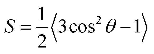
Bottom-up approaches are direct ways to synthesize horizontally aligned 2D nanomaterials. They allow the fabrication of films of controlled sizes, thicknesses and orientation, which make them convenient and scalable routes.15 Besides chemical vapor deposition (CVD), other representative chemical methods that can grow oriented 2D nanomaterials from small molecules are hydrothermal synthesis and gelation growth.15,147–152 For example, hydrothermal or solvothermal synthesis methods are classical wet-chemical routes for nanomaterials, especially the inorganic ones.153,154 They are conducted in a sealed vessel, where the reaction medium is water for hydrothermal and an organic solvent for solvothermal reactions. The principle of the synthesis is to heat the reaction medium above the boiling temperature of the solvent to generate high pressure, which leads to the reaction and growth of nanocrystals. By using a hydrothermal method, Xu et al. synthesized horizontally aligned 2D hybrid sheets of V2O5 and reduced graphene oxide (rGO/V2O5) (Fig. 8a1), which can be utilized as cathodes for lithium-ion batteries.155 As shown in Fig. 8a2, the 2D hybrid sheets exhibited a wrinkled surface, which increased the accessible surface area for ion interaction. In addition, the cross-sectional SEM image revealed well-defined horizontally oriented layers made of 30 nm-thick nanosheets (Fig. 8a3).
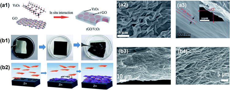 |
| | Fig. 8 Horizontal alignment of 2D materials by a bottom-up approach. (a1) Schematics of the hydrothermal fabrication process of rGO/V2O5 hybrid sheets. (a2) Top view SEM image of rGO/V2O5 hybrid sheets showing a wrinkled surface. (a3) The cross-sectional SEM image showing individual layers. Reproduced from ref. 155 with permission from the Royal Society of Chemistry. (b1) Schematic representation of the interfacial gelation mechanism where a Zn foil (in grey) is immersed in a GO dispersion (black). (b2) Graphene gelation mechanisms at the surface of the metallic foil. (b3 and b4) Morphologies of the graphene aerogels. Reproduced from ref. 158 with permission from John Wiley and Sons. | |
Another typical wet-chemical strategy for directional 2D nanomaterial assembly is gelation growth.151,152 It is a simple and straightforward way to assemble macroscopic structures from nanosheets. For example, Yang et al. reported the ordered gelation of graphene hydrogel films from chemically converted graphene in water without the need for additional gelators.156,157 Later, Maiti et al. demonstrated the successful fabrication of reduced graphene oxide films in μm-thick hydrogels with porous and planarly aligned microstructures.158 To obtain this structure, Zn foils were immersed in a mildly acidic GO dispersion to induce the spontaneous growth of graphene hydrogels on the Zn surface (Fig. 8b1). The mechanism of this spontaneous interfacial gelation can be explained by the reduction process as shown in Fig. 8b2. Because of the lower reduction potential of Zn, there is continuous electron transfer from the Zn metal surface to the GO. As a result, ionized Zn2+ tightly attaches to the negatively charged GO nanosheets, leading to layer-by-layer interfacial stacking at the basal planes (Fig. 8b3 and b4). Generally, the gelation growth thickness is controlled by the immersion time: a 78 μm-thick gel film can be typically obtained within one hour. At the same time, the lateral dimension of the graphene film is determined by the substrate, making the procedure scalable.
3.1.6 Hot-pressing.
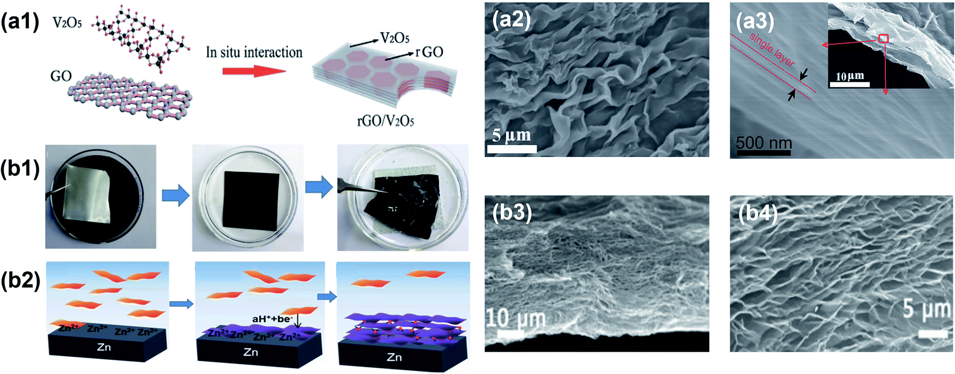
Hot-pressing, which consists in simultaneously applying heat and pressure, is a popular fabrication method to assemble nanomaterials when high relative density is required. Under uniaxial pressure, a planarly oriented microstructure can be formed from pre-stacked nanosheets. Or in other cases, a self-aligned texture can be formed during sintering due to the uneven stress distribution around nanosheets.159–162 Using this method, Liu et al. fabricated aligned graphene/polycarbonate composites with multiple parallel layers.163 For planar stacking, each layer thickness was exponentially scaled with successive stacking and folding in a quadrant, and hot-pressing could further improve the interlayer integration (Fig. 9a1). After repeating the process, multi-layered graphene composites were obtained, presenting closely spaced and horizontally aligned layers (Fig. 9a2). As a result, the elastic modulus and strength were significantly enhanced at exceptionally low volume fractions of only 0.082%. Other than pre-stacking and compressing, 2D nanomaterials can be alternatively assembled into a complex precursor such as granular particles, where nanosheets are aligned around a sphere, before being hot-pressed. Zhang et al. reported a thermally conductive but electrically insulating segregated double network in graphene/h-BN-based composites via hot-pressing.164 Further hot compressing treatment into thinner sheets can improve the intrinsic filler orientation. Additionally, the hot-pressing synthesis procedure is scalable, allowing the fabrication of a dense product with controllable thickness.
 |
| | Fig. 9 Horizontal alignment of 2D nanomaterials by (a) hot-pressing and (b) Langmuir–Blodgett assembly. (a1) Stacking and hot-pressing method for planar composites. (a2) SEM images of the planar composites with different layer thickness. Reproduced from ref. 163 with permission from the American Association for the Advancement of Science. (b1) Schematic representation of a conventional Langmuir–Blodgett process and electrospray. (b2) Water-dispersed graphene sheets on a Si wafer by electrospray at increasing surface pressures. Reprinted with permission from ref. 169. Copyright (2015) American Chemical Society. | |
3.1.7 Langmuir–Blodgett (LB) assembly.
The LB method is a classical interfacial assembly strategy that is performed at the liquid–air interface.165–168 Typically, molecules or nanosheets are initially dispersed in a water-immiscible volatile organic solvent. Then, the dispersion is spread dropwise onto the water surface. After the solvent has evaporated, a water-supported thin layer is formed, which can be later transferred to a substrate and compressed. When it comes to controlled horizontal alignment of 2D nanosheets, the LB method has been further developed by tuning the dewetting instability of the wet monolayer upon transferring, which involves the wet transition from complete to partial wetting. Consequently, the alignment and patterning design of 2D nanomaterials can be accessible without an additional template.169–171 Kim et al. investigated the edge-to-edge interactions between neighbouring graphene oxide sheets via LB assembly.168 In this case, the water surface was utilized as an ideal platform to assemble the 2D nanosheets. To improve the spread capability of nanosheets by LB methods, Nie et al. developed a general method by combining it with electrospray (Fig. 9b1).169 Benefiting from the reduced volume of the aerosolized droplets, the diminished droplets are depleted rapidly in the initial spreading and leave all the nanoparticles on the water surface, leading to efficient LB assembly as shown in Fig. 9b2.
3.2 Vertical microstructures
The anisotropic properties of 2D nanomaterials are some of the most critical features to achieve unique functionalities. When they are aligned vertically, the 2D nanosheets can provide more reaction sites from the exposed edges as compared to when they are horizontally aligned. Also, the increased surface area resulting from vertical alignment in a forest-like configuration can for example lead to more efficient conduction pathways. In this section, we review several representative strategies to achieve the vertical alignment of 2D nanomaterials. The typical processing, achieved structures, advantages and limitations of the techniques are tabulated in Table 3. Some universal techniques are capable of conducting diverse aligned patterns including horizontal and vertical structures and will be tackled in the arbitrarily aligned section.
Table 3 Processing techniques for vertical alignment of 2D nanomaterials
| Method |
Alignment technique |
Achieved structure |
Advantages |
Limitations |
Ref. |
| Tape casting |
Induction of vertically oriented torque by horizontally shearing with a blade on solution containing liquid-crystalline nanosheets |
Film, vertically packed nanosheets |
Scalable, nearly thickness-independent |
Slow processing |
116, 180, 182 and 185 |
| Extrusion |
Alignment of 2D nanoparticles along the extrusion direction through a die and cutting perpendicularly to this die |
Tube, vertically oriented nanosheets |
Flexible alignment direction |
Requires specific equipment and post-processing (cutting) |
119 and 183 |
| Laser irradiation |
Irradiation of a high energy laser on the surface of a nanosheet film to induce local compression forces |
L-shaped nanostructures in thin films |
One-step process, local control enabling patterning possibility, reduces nanosheet defects |
Requires equipment for laser generation |
186
|
| Hydrothermal/solvothermal synthesis |
Bottom-up nanostructure growth on a substrate in solution |
Film, direct vertical alignment, densely packed nanostructure |
Versatile and cheap, direct growth of nanostructures, low reaction temperature |
Requires autoclave equipment and proper safe operation |
192, 200 and 202 |
| Templated growth |
Template induced nanostructure crystallization and growth on pre-fabricated supports |
Film, densely packed nanostructure |
Tunable particle size, highly interconnected nanostructures |
Requires pre-fabricated templates and precise control of template growth |
58 and 201 |
3.2.1 Shear force.
Achieving vertical alignment of 2D nanomaterials is considered more difficult than horizontal alignment since gravitational forces need to be overcome. Shear resulting from flow-induced fluctuations in smectic or lamellar self-assembled colloidal phases is one effective route. This shear-induced orientation depends on the torque that is generated perpendicularly to the shear direction.116,180 Tape casting is a typical technique to shear. Assisted by tape casting, highly ordered horizontal structures have been obtained as mentioned above (Fig. 7b). Nevertheless, tape casting can also lead to vertical alignment of 2D nanosheets under controlled conditions (Fig. 10a1). When 2D nanosheets are well-dispersed in aqueous solution, long-range oriented mesophases spontaneously form as discotic liquid crystal phases, where the nanosheets are aligned parallel to each other.140,181 Under external mechanical shear, a vertical torque arising from the flow-induced fluctuation is generated, which orients the aligned nanosheets in the mesophases, vertically (Fig. 10a2 and a3).116,180,182 The applied shear rate for vertical orientation should be adjusted according to the particle size, with larger particles requiring a lower shear rate.116 Furthermore, extrusion is another method to induce shear. As one of the most commonly used processing techniques in the plastics industry, it is also suitable for orienting 2D nanomaterials having high anisotropy.183 A typical extrusion process is illustrated in Fig. 10b1. The critical control parameters to achieve good distribution and orientation of 2D nanosheets include a relatively low processing temperature, suitable draw ratios (the ratio between extrudate pulling velocity and average velocity in the extrusion die), sufficiently high local shear rates and shear stresses inside the die for orientation. After extrusion, cutting along the transverse section is required to reveal the vertically aligned nanoflakes (Fig. 10b2). By providing a biaxial stress field by combining rotation and extrusion, the 2D nanoflakes could be further assembled into perpendicular alignment to the radial direction (Fig. 10c1–c3).184
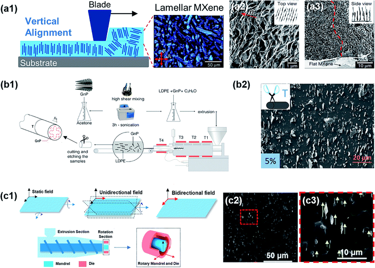 |
| | Fig. 10 Vertical alignment of 2D nanomaterials assisted by shear force. (a1) Schematic representation of tape casting of liquid-crystalline Ti3C2Tx. Reproduced from ref. 185 with permission from Elsevier. (a2) Top view SEM image of the MXene lamellar liquid crystal (MXLLC). (a3) Side view of vertical MXene nanosheets. Reproduced from ref. 116 with permission from Springer Nature. (b1) Schematic representation of the extrusion process of graphite nanoplatelet (GNP) and polyethylene (LDPE) nanocomposites. (b2) Surface morphology of the extruded GNP–LDPE composite with the transverse section. Reproduced from ref. 183 with permission from John Wiley and Sons. (c1) Schematic illumination of the rotation extrusion equipment. (c2) Cross-sectional SEM images of the extruded composites. (c3) Magnified area of (c2) in which yellow arrows refer to the nanofiller alignment direction. Reproduced from ref. 184 with permission from Elsevier. | |
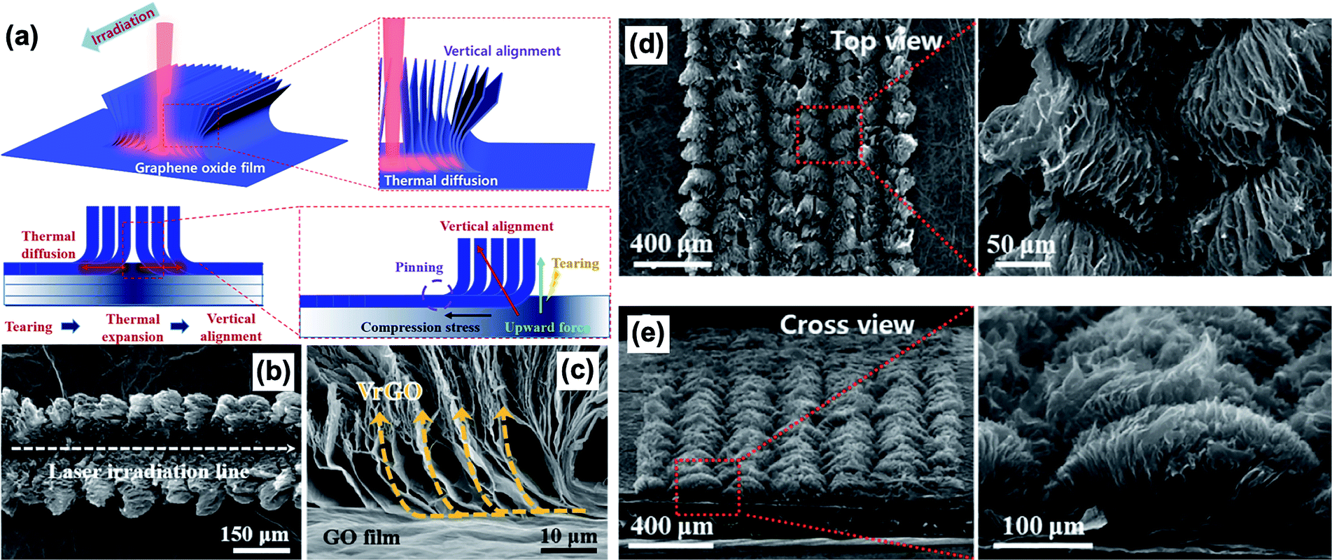
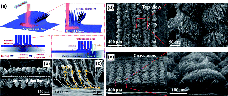
3.2.2 Laser irradiation.
Laser irradiation is a newly developed technique to process and orient 2D nanomaterials.186–188 Thanks to the recent development of a diverse range of lasers, laser irradiation as a method to process nanomaterials is blooming.189–191 Different from most conventional material processing techniques, laser irradiation imparts rapid heat and localized high energy to materials, allowing precise control over the material microstructures.188 Park et al. reported the fabrication method of L-shaped graphene nanostructures with a vertical alignment and reduced defect level through laser irradiation.186Fig. 11 presents the fabrication process of laser-induced L-shaped graphene nanostructures. Initially, a horizontally aligned GO film was prepared by filtration. Then, as the laser irradiated the surface of the horizontally stacked GO film, compression stresses generated because of thermal expansion of individual GO nanosheets. As a result, the GO nanosheets were locally re-aligned in the vertical direction. Also, the high energy density from CO2 lasers could even heal the defects within the graphene nanosheets by removing the oxygen-containing functional groups. The as-fabricated L-shaped graphene nanoarchitectures exhibited high hydrophobicity, excellent electron transport and thermal conduction due to the localized vertical orientation and lower defect level.
 |
| | Fig. 11 Vertical alignment of reduced graphene oxide nanosheets by laser irradiation. (a) Schematic of the CO2 laser irradiation fabrication process of the vertically aligned nanostructure. (b and d) Top view of the vertically aligned nanosheets. (c and e) Cross-sectional view of the as-fabricated nanostructure. Reproduced from ref. 186 with permission from Elsevier. | |
3.2.3 Hydrothermal and solvothermal synthesis.
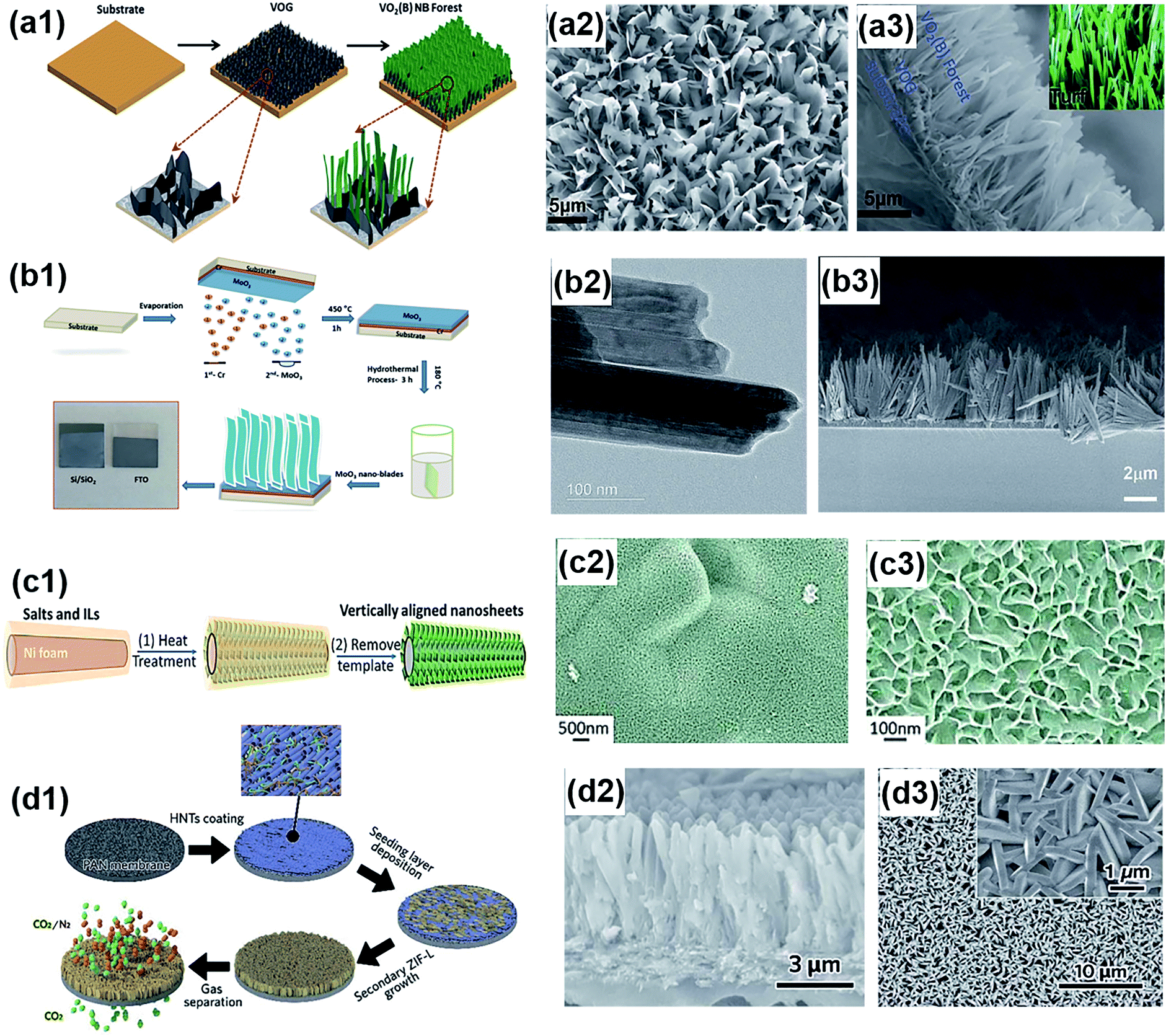
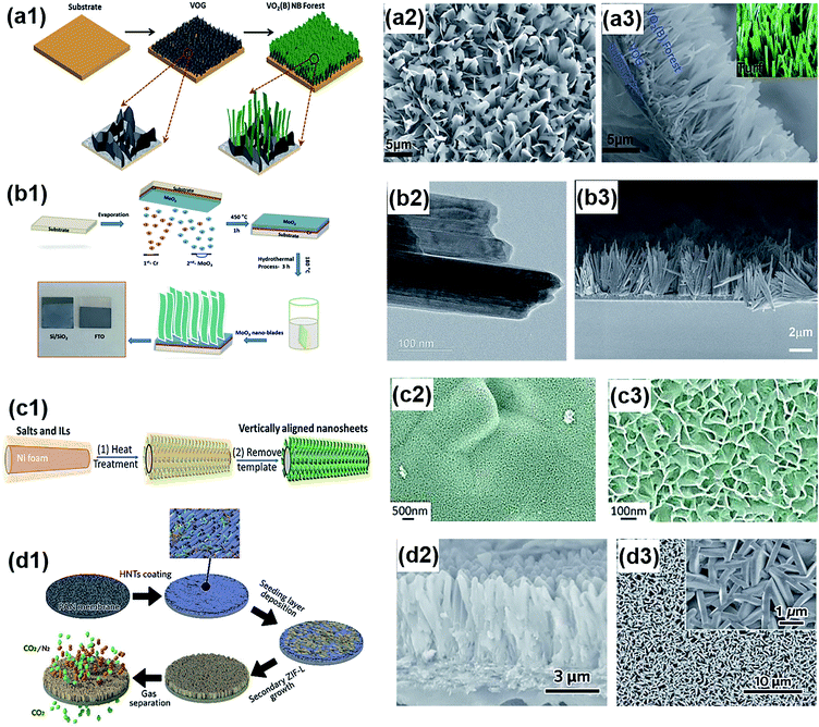
The hydrothermal and solvothermal synthesis strategies introduced in Section 3.1.5 to produce horizontal layers (Fig. 8a) can also create vertically aligned nanosheets. Through a hydrothermal reaction, vertically aligned nanosheets have been grown on various substrates under well-controlled growth parameters and are applicable to diverse material types and geometries such as nanowires, nanospheres, nanosheets, and nanoribbons.192–196 Generally, the morphology of the grown nanostructures can be tuned by controlling the template seed growth, reaction temperature, pH and by adding surfactants.197–199Fig. 12a1 displays a typical solvothermal synthesis procedure for vertically oriented VO2(B) nanobelts.200 Before solvothermal growth, a thin layer of vertically oriented graphene was grown on a flat substrate by plasma enhanced CVD, which improved the vertical growth of the nanobelts into a forest structure with enhanced densification. Later, the precursor slurry was loaded on the graphene coated substrate in an autoclave, in which the densely packed nanostructure self-assembled with a vertical orientation as shown in Fig. 12a2 and a3. Similarly, vertical alignment of α-MoO3 nano-blades was achieved by the hydrothermal method (Fig. 12b1). The obtained nano-blades were arranged in rows and bundles, showing a flower-like structure. The individual nano-blades were 10 to 50 nm-width without stacking onto each other (Fig. 12b2 and b3).
 |
| | Fig. 12 (a1) Schematic showing the solvothermal synthesis of VO2(B) nanobelts (NB) on a vertically oriented graphene (VOG)-coated substrate. (a2) Top morphology of aligned VO2(B) nanobelts. (a3) Cross-sectional SEM image of grown VO2(B) nanobelts. Reproduced from ref. 200 with permission from the Royal Society of Chemistry. (b1) Schematic representation of the hydrothermal synthesis process of vertically aligned α-MoO3 nano-blades. (b2) HRTEM image of α-MoO3 nano-blades. (b3) SEM image showing vertical alignment of α-MoO3 nano-blades. Reproduced from ref. 192 with permission from the Royal Society of Chemistry. (c1) Schematic illustration of the salt-templating process for vertically aligned 2D nanosheets. (c2 and c3) Typical morphologies of the grown graphitic carbon nanosheets. Reprinted with permission from ref. 201. Copyright (2015) American Chemical Society. (d1) Schematic illustration of the halloysite nanotube (HNT) modification on a polyacrylonitrile (PAN) membrane and templated growth of vertically aligned zeolitic imidazolate framework-L (ZIF-L) 2D MOF nanosheets. (d2) Cross section and (d3) top surface of the vertically aligned MOF membrane. Reproduced from ref. 58 with permission from the Royal Society of Chemistry. | |
3.2.4 Templated growth.
The synthesis of vertically aligned 2D nanosheets can also be implemented by the self-assembly of sacrificial particles called templates. Typically, the nanostructures fabricated by template induced self-assembly exhibit highly interconnected nanostructures, strong interface adhesion, good structural robustness, etc. For example, Zhu et al. investigated a general salt-templating method that led to vertically oriented graphitic carbon nanosheets.201Fig. 12c1 presents the schematic illustration of the salt-templating process. In short, the precursor was mixed with a ZnCl2 and KCl salt mixture before being coated onto a nickel foam substrate. After heat treatment and template removal, vertically aligned and highly interconnected nanosheets were obtained (Fig. 12c2 and c3). In this case, the formation of vertical orientation of the 2D nanosheets could be attributed to two reasons. One is the nickel induced dissolution and crystallization of carbon on the surface of the substrate, leading to the directional growth of graphitic carbon distal to the surface. The other reason is that the salt mixture acts as a porogen and helps in forming separated flat structures. In another example, Li et al. reported templated growth of vertically aligned 2D metal–organic framework (MOF) nanosheets (Fig. 12d1–d3).58 To achieve the nanocrystal orientation, a layer of horizontally aligned 1D halloysite nanotubes was deposited as the nucleation sites for 2D MOF nanosheets. This pre-fabricated layer also plays a role in guiding the vertical growth of nanosheets.
3.3 Heterogeneous microstructures
Beyond purely horizontal or vertical alignment, the creation of more complex microstructures with ordered 2D nanomaterials can also generate novel functionalities. The heterogeneous architectures are typically beneficial for enhancing interfacial interactions of ion diffusion by increasing the density of reaction sites, which may facilitate applications such as catalysis, energy storage and so on. In this section, we review several emerging approaches used to fabricate heterogeneous microstructures as summarized in Table 4. By using different synthesis technologies, diverse periodic textures and microstructures can be effectively tuned.
Table 4 Processing techniques for heterogeneous microstructures with 2D nanomaterials
| Method |
Alignment technique |
Achieved structure |
Advantages |
Limitations |
Ref. |
| Crumpling |
Induction of compressive stresses in a film of horizontally aligned nanosheets |
Crumpled film |
Facile method, controllable crumpled patterns |
Limited scale (e.g., micrometer-scale), time consuming |
59 and 207–209 |
| Scrolling |
Scrolling of layered nanosheets into fibers |
Fiber, spiral structure |
Simple procedure, high packing density, unlimited material type |
Requires precise operation |
118, 163 and 212 |
| Layer-by-layer assembly |
Sequential deposition of individual layers into a multilayer structure |
Film, multiple layers |
Simple procedure, low cost, precise film thickness control |
Requires strong interaction between individual layers, slow fabrication speed |
129, 213, 216 and 219 |
| Freeze-drying assisted self-assembly |
Self-assembly of liquid crystals under appropriate conditions |
Film/bulk |
Simple procedure, inherently interconnected microstructure |
Requires precise control of liquid crystal alignment conditions |
205, 218 and 220 |
3.3.1 Crumpling.
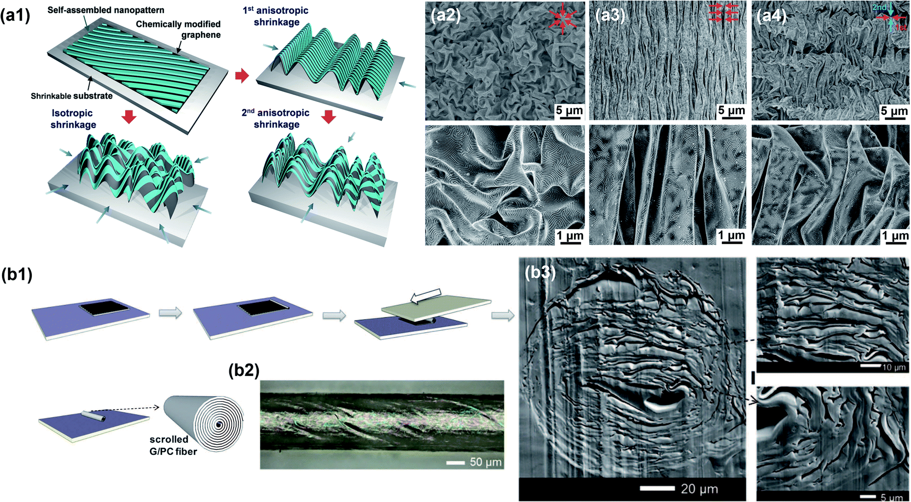
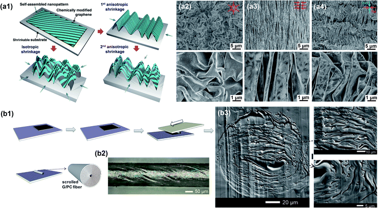
2D nanomaterials have a large surface area and tunable surface functionalities. They are much easier to bend or fold than stretch in the planar direction, leading to morphological surface instability.203,204 This mechanical instability has been further utilized to create 3D crumpled architectures with the assistance of external stimuli. Crumpled graphene films, as an example, are extensively studied for energy storage, electronics, biomedicine, etc., where the crumpling degree is pivotal in determining their performances.205,206 To crumple a graphene film, this film is first adhered on a pre-stretched elastomeric polymer substrate or any other substrate able to shrink. When the substrate relaxes, it shrinks, inducing compression in the graphene layer that crumples due to its high stiffness (Fig. 13a1).59,207–209 Furthermore, the substrate shrinkage can be controlled to be isotropic or anisotropic. For isotropic shrinkage, the sample is simply annealed without mechanical stress, showing a flower-like crumpled morphology (Fig. 13a2). As for anisotropic, uniaxial and hierarchical crumpling, the relaxation of the substrate is conducted by anchoring one of its side during the shrinkage (Fig. 13a3 and a4).59 The crumpled patterns are typically on a sub-micro scale, which are applicable for various applications such as electrochemical catalysis, strain sensors and stretchable conductors.210,211 The crumpling method could be more suitable for synthesizing small sample sizes rather than scalable products to precisely control the shrinkage of substrates.
 |
| | Fig. 13 Heterogeneous graphene nanostructures created by (a) crumpling and (b) scrolling. (a1) Schematic illustration of crumpling for a self-assembled nanopattern. SEM images of (a2) isotropically, (a3) uniaxially, and (a4) hierarchically crumpled graphene with different shrinkage directions specified in red arrows. Reproduced from ref. 59 with permission from John Wiley and Sons. (b1) Schematic illustration of scrolling the graphene/polycarbonate (G/PC) nanocomposite. (b2) Optical microscope image of the scrolled fiber. (b3) Cross-sectional SEM images of the scrolled fiber. Reproduced from ref. 163 with permission from the American Association for the Advancement of Science. | |
3.3.2 Scrolling.
Scrolling is a simple way to assemble 2D nanomaterials into fibers with a heterogeneous structure, which typically shows a spiral cross section. It provides broad material selection without specific requirements of the composition, chemical bonding or nanomaterial dimension. During scrolling, a planar film containing ordered nanosheets is rolled into a cylinder. The dimensions and intrinsic microstructure of the cylinder can be easily controlled by varying the initial film parameters, such as thickness and orientation.118,163Fig. 13b1 provides an example of the transverse shear scrolling method. Liu et al. demonstrated the feasibility of this method for fabricating closely packed spiral microstructures in graphene-based nanocomposites (Fig. 13b2 and 13b3).163 The scrolled graphene nanocomposites with a heterogeneous structure exhibited anisotropic electrical conduction along the graphene planar axis with electrical conductivity about 4 S cm−1 at a low volume fraction of about 0.185%, and the transparency was maintained at the same time. Similarly, Chen et al. reported the fabrication of tightly packed and interconnected BN nanosheet composites using scrolling.212 These nanocomposites exhibited an enhanced through-plane thermal conductivity of 1.94 W m−1 K−1 with 15.6 vol% BN nanosheets, which are beneficial for thermal management applications. The heterogeneous structures of 2D nanomaterials synthesized by scrolling are typically fibers on a micro- or milli-meter scale, which are still challenging for industrial fabrication.
3.3.3 Layer-by-layer (LBL) assembly.
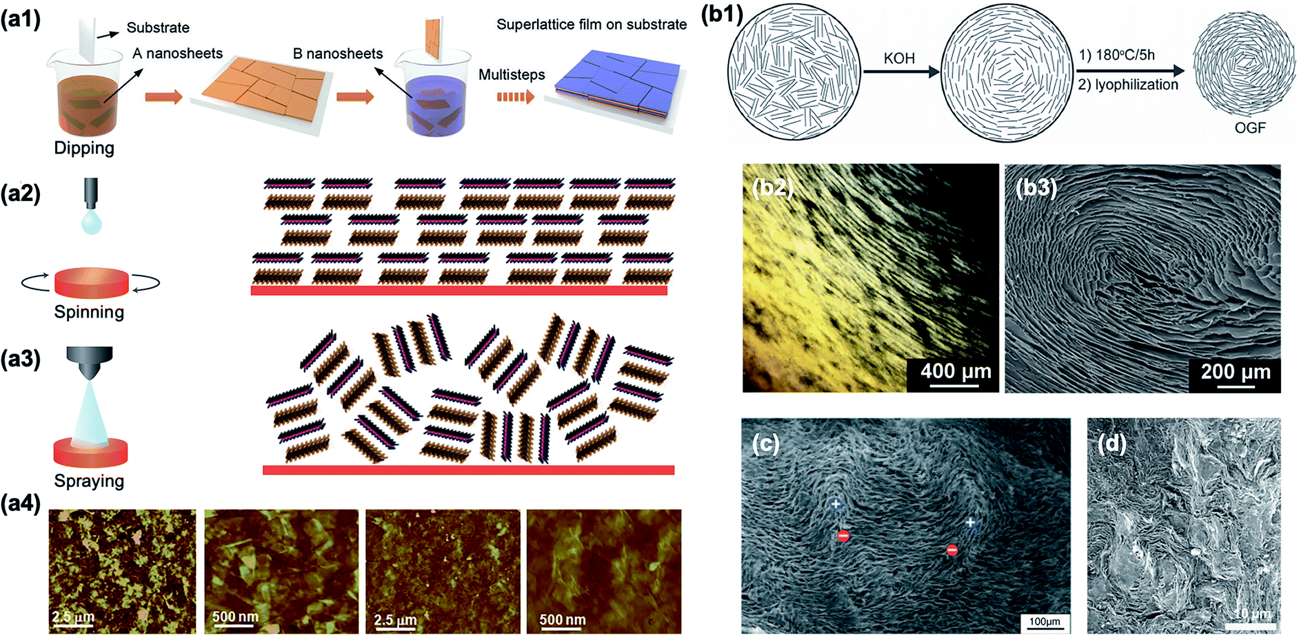
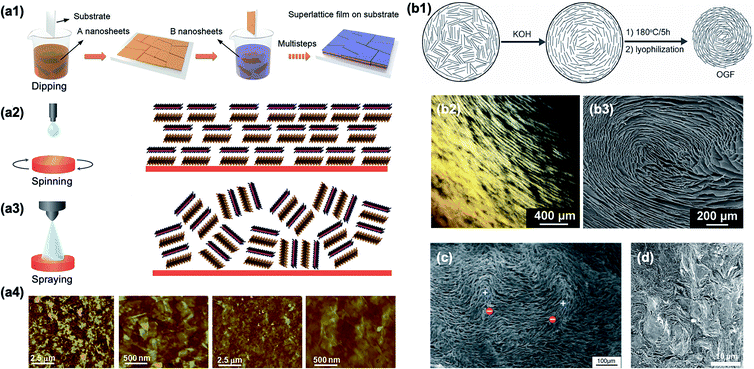
Layer-by-layer (LBL) assembly is one of the most extensively used methods for synthesizing nanocomposites with heterogeneous compositions and structures at high filler loadings. It consists in assembling individual layers of nanoparticles in a sequential manner, thereby allowing for the fabrication of building heterogeneous structures composed of different components. LBL assembly is thus a versatile approach to combine individual layers of various morphologies or different material types, where the film thickness can be precisely controlled.213–215 In practice, the LBL assembly is realized using dipping, spinning or spraying as shown in Fig. 14a1–a3. In a typical LBL dipping assembly procedure, a substrate is sequentially immersed into colloidal solutions containing nanosheets. A heterogeneous film with a multilayer structure can be formed by repeating the dipping process.320 The formation of a layered structure with high ordering is closely related to the strong interactions between individual components, such as electrostatic force, covalent bonding, hydrophobic interaction and so on.129,213 To guarantee high LBL packing, the deposited material components should be selected to bound together. This can be improved by introducing surface modifications such as functional groups or surfactants. For example, Lee et al. utilized the spin coating LBL method to assemble positively charged rGO and negatively charged rGO as one bilayer. A multilayer structure with 10 bilayers was obtained by repeating the procedures (Fig. 14a4).216 The size and thickness of the fabricated structures are set by the substrate dimensions and repeat times, respectively, which provide the possibility for scale-up applications.
 |
| | Fig. 14 Fabrication approaches of heterogeneous structures. (a1) LBL assembly of oppositely charged nanosheets by dipping. Reproduced from ref. 219 with permission from John Wiley and Sons. Schematic illustration of various LBL methods via (a2) spinning and (a3) spraying. Reproduced from ref. 213 with permission from Springer Nature. (a4) AFM images showing the surface morphologies of rGO multilayers fabricated by spin coating. Reproduced from ref. 216 with permission from the Royal Society of Chemistry. (b1) Schematic illustration of the self-assembly of ordered graphene foams (OGFs) by tuning the pH value. (b2) Polarized-light optical microscope (POM) image of GO suspension near the inner surface of the glass tube. (b3) SEM image showing the heterogeneous structure of OGFs. Reproduced from ref. 218 with permission from John Wiley and Sons. (c) SEM image of a graphene oxide liquid crystal treated by freeze-drying. Blue and red symbols represent +1/2 and −1/2 disclinations, respectively. Reproduced from ref. 220 with permission from John Wiley and Sons. (d) SEM image of a self-assembled MXene liquid crystal. Reproduced from ref. 116 with permission from Springer Nature. | |
3.3.4 Freeze-drying assisted self-assembly.
2D nanomaterials with high aspect ratios can be self-assembled into aligned domains when they are in the liquid crystal form. Liquid crystals (LCs) are particles in the intermediate state between an amorphous liquid and crystalline solid. LCs therefore exhibit mobility and self-assembled ordering under competing driving forces from packing and orientation entropies. The LC size, concentration, repulsion and solvent viscosity greatly influence their self-assembling behavior.217 Furthermore, with the assistance of freeze-drying, which provides rapid growth of ice crystals, the self-assembly of 2D nanosheets from dilute LC suspension can be induced by concentrating the LCs between the crystals. As an example, Yao et al. organized GO nanosheets into LCs with high heterogeneous orientations by increasing the pH value of their dispersion with potassium hydroxide (KOH) (Fig. 14b1).218 The self-assembled nanosheets exhibited an inherently interconnected microstructure. In strong alkaline bases such as KOH, the enhanced electrostatic repulsion between GO sheets could be increased, leading to higher fluidity and a highly ordered texture. After hydrothermal reduction of GO LCs and subsequent freeze-drying, a spiral microstructure with better aligned nanosheets was obtained mainly due to the alignment of GO nanosheets in LCs along the inner surface of the container (Fig. 14b2 and b3). More examples of self-assembled macroscopic orientation of liquid crystals can be found in Fig. 14c and d. Overall, the freeze-drying assisted self-assembly method involves simple procedures but may be limited in scalability and material diversity because it requires more strict control of nanomaterial selection and operation with a suitable size, aspect ratio, materials chemistry and fabrication parameters to achieve desirable assembled microstructures.
3.4 Arbitrary microstructures
The orientation and distribution of 2D nanomaterials are key factors that determine the macroscopic performances of films and bulk materials made from them due to their anisotropic properties. These performances include mechanical, electrical, thermal, optical properties and so on. Therefore, methods capable of controlling the microstructure in predesigned orientation patterns are highly desirable. The methods that can create arbitrary microstructures are therefore reviewed in this section, and their representative features are summarized in Table 5. Through these technologies, a variety of aligned patterns can be achieved within a single method, allowing materials with a highly tunable local orientation and versatile properties.
Table 5 Processing techniques for arbitrary orientation
| Method |
Alignment technique |
Achieved structure |
Advantages |
Limitations |
Ref |
| Magnetic field |
Application of external magnetic fields to align 2D nanosheets having anisotropic magnetic susceptibility |
Bulk/film, highly tunable localized orientation |
Low cost, applicable to a wide material type, any orientation angle |
Limited scaffold density, the sample dimension is limited by the magnet size |
42, 60, 222 and 225 |
| Electric field |
Application of an external electric field to align 2D nanosheets having anisotropic electric susceptibility |
Bulk/film, tunable control of local particle alignment |
Low cost, scalable, facile to tune electric field distribution |
Requires dielectric polarization and requires a multi-step process for complex patterns |
231–233
|
| Freeze casting |
Control nucleation and directional growth of ice crystals under temperature gradients to push the 2D nanosheets into patterns |
Bulk/film, porous scaffolds, well-orientated patterns |
Applicable to a wide range of materials, scalable, tunable microstructures of freeze-cast scaffolds |
Limited scaffold density, requires precise control of solidification front growth |
49, 240–242 and 255 |
| CVD |
Gaseous chemical reaction and solid deposition on a substrate surface |
Film, tunable aligned structure through growth conditions |
Scalable, high material quality |
Limited layer thickness, cannot change orientation angle freely |
55, 247–249, 251 and 252 |
3.4.1 Magnetic field assisted orientation.
A magnetic field is a powerful tool in precisely and remotely controlling the local orientation of anisotropic particles, including 2D nanomaterials.60,220,221 This approach utilizes external magnetic fields to align particles with anisotropic magnetic susceptibility suspended in a liquid matrix.222,223 As 2D nanomaterials are often diamagnetic, extremely high magnetic fields are usually required for alignment.222,224 To solve this problem, superparamagnetic nanoparticles such as iron oxide nanoparticles can be coated on the surface of the nanosheets to make them more responsive to magnetic fields.225,226 During magnetic alignment in suspension, the dynamics of particles is synergically controlled by torques generated from the magnetic, gravitational, and viscous forces. Several key factors can influence the particle orientation, including the particle geometry, magnetic field strength and gradient, particle concentration and fluid viscosity. After positioning the particles, the fluid is consolidated to fix the orientation, which can be achieved by solvent evaporation, light or temperature-controlled curing, depending on the solvent type.42,223,226–228 To create complex local assemblies, virtual magnetic molds can be used.319 These molds consist in placing a ferromagnetic material above a magnet. The ferromagnetic material then becomes magnetized and attract the particles locally. Combined with a dynamic magnetic field instead of a static field, 2D particle orientation in set directions with a local particle concentration can be achieved. Fig. 15a shows the alignment process of gelatin-based composites containing magnetically responsive reduced graphene oxide (m-rGO) flakes.60 By controlling the magnet placement and by using a virtual magnetic mold made of a Co or Ni template, both the orientation and spatial distribution of m-rGO flakes can be effectively tailored within the composites. By choosing predefined meshes as the template, the m-rGO flakes could be assembled into hierarchical double-percolating networks (Fig. 15b), enabling both optical transparency and electrical conductivity at a reduced percolation threshold of 0.65 to 0.85 vol% of rGO. In addition, Lin et al. demonstrated the magnetic response and alignment of graphene flakes, where the displayed patterns of graphene suspension were induced by different shapes and configurations of magnets (Fig. 15c–f).222 Later, when the static magnetic field was switched to a rotating magnetic field in the x–y direction (Fig. 15g), the graphene nanosheets were aligned in the planar direction, exhibiting much higher birefringence and anisotropic absorption/transmission capabilities than those without a magnetic field or with a static magnetic field (Fig. 15h–j). Overall, the magnetic orientation of 2D nanomaterials is applicable to a wide range of material chemistry and the orientation angle can be easily programmed by changing the direction of the magnetic field, while the sample dimension is usually limited by the magnet size.
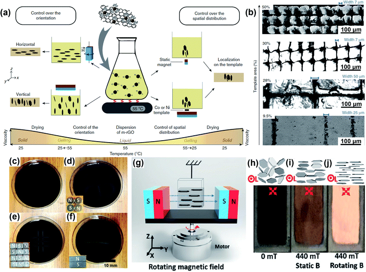 |
| | Fig. 15 Controlled orientation of 2D nanomaterials assisted by a magnetic field. (a) Schematic illustration of magnetic control over the orientation or spatial distribution of magnetized reduced graphene oxide (m-rGO) flakes. (b) Optical micrographs of patterned poly(2-acrylamido-2-methyl-1-propanesulfonic acid) (PAMPS) composites with 0.065 vol% magnetically responsive rGO flakes of decreasing template area and various line widths. Reproduced from ref. 60 with permission from Springer Nature. Photographs of 0.1 wt% graphene suspension with (c) no magnet field and (d–f) magnets of different shapes and configurations placed underneath for magnetic field sensing and display. Reproduced from ref. 222 with permission from John Wiley and Sons. (g) Schematic of the experimental setup to generate a rotating magnetic field for planar alignment of graphene sheets. (h–j) Schematic representation and snapshots of white light birefringence/transmission images of graphene suspension under different magnetic field conditions: (h) without a magnetic field, (i) under a static magnetic field in the x–y direction, and (j) under a rotating magnetic field in the x–y plane. The symbol L represents the incident white light in the x direction. Reproduced from ref. 221 with permission from John Wiley and Sons. | |
3.4.2 Electric field assisted orientation.
Similar to magnetic fields, electric fields can serve as an external driving force to align anisotropic particles in programmable directions. Electric field induced alignment is compatible with dielectric materials or electrically conductive fillers, such as graphene nanoplatelets, graphite, BNNSs or fluorohectorite nanosheets, which are typically mixed in a low viscosity, organic medium.229,230 These 2D nanomaterials can respond to the electric field and form oriented patterns because they can be polarized by the external field and acquire a dipole moment. During the electrical alignment, a high-frequency alternating current (AC) electric field is commonly used to orient 2D nanomaterials and also avoid the electrophoresis of nanosheets and the electrolysis of the medium.231,232 Under this alternating AC electric field, any solid inclusion suspended in a dielectric liquid will be polarized and acquire a dipole moment because of the mismatch in dielectric properties and electrical conductivity between the particles and their surrounding matrix. For 2D nanomaterials with considerable anisotropy, the polarization moment generally develops along their basal plane. When the polarization moment is not aligned along the electric field, a torque is created that rotates the particles and align their basal plane along the electric field direction to reach an equilibrium state. Once aligned, the polarized nanosheets can attract each other due to opposite surface charges, leading to an end-to-end chain configuration (Fig. 16a–d).233 Theoretically, similar to magnetic alignment, the electric field induced alignment method can achieve arbitrary orientation directions, simply by tuning the electric field. For example, complex and intricate ordered patterns can be fabricated by sequential electric field induced orientation and photolithographic consolidation (Fig. 16e–j).232 Moreover, the electric field induced alignment of 2D nanomaterials should be differentiated from the electrophoretic deposition (EPD) for materials like rGO or MXenes, in which the charged particles cannot be polarized but will move towards the electrode of opposite polarity and deposit on the surface.234–236
 |
| | Fig. 16 Controlled orientation induced by an electric field. (a–d) Optical micrograph images of graphene nanoplatelet alignment in liquid epoxy resin by an AC electric field (E) as a function of time (0 to 20 min). (a) Random orientation of graphene nanoplatelets before applying an electric field, and after applying an electric field for (b) 4 min, (c) 10 min and (d) 20 min. Reproduced from ref. 233 with permission from Elsevier. (e) Schematic representation of a patterned anisotropic hydrogel by multi-step electrical orientation and photolithographic polymerization with different electric field (E) directions and use of ultraviolet (UV) light. (f and g) Polarizing optical microscope (POM) images showing hydrogel patterns with different nanosheet alignments. A: analyzer, P: polarizer, and Z′: axis of the tint plate. (h–j) Photos of the patterned anisotropic hydrogels. Reproduced from ref. 232 with permission from Springer Nature. | |
3.4.3 Freeze casting.
Freeze casting, also known as ice templating, is a well-established technique that is utilized to fabricate arbitrarily oriented patterns, such as horizontal, vertical, gradient, layered, honeycomb, and radial structures.49,237–239 It is a versatile technique applicable to diverse material types not limited to 2D nanosheets. The four processing steps of a typical freeze casting procedure are liquid suspension preparation, solidification, sublimation and post-treatment as shown in Fig. 17a.240 A dispersant, plasticizer and binder are commonly added in the initial liquid suspension to ensure uniform dispersion of the 2D nanoparticles in the liquid medium. The microstructure is determined by the formation of ice dendrites during the solidification stage. After sublimation of the ice, the subsequent post-treatment, such as sintering densification, thermal reduction or pyrolysis, will transform the material into a porous scaffold. The desirable oriented patterns are thus set during the solidification, when the suspended particles are rejected by the moving solidification front, concentrated and entrapped between the ice crystals. Fig. 17b illustrates the freezing front progression at different velocities, where v is the particle freezing front velocity, and vcr is the ice critical freezing front velocity. At a very low solidification velocity (v ≪ vcr), the particles are not rejected by the ice front, so that no pattern forms. At v < vcr, the particles are generally rejected and assemble in a lamellar microstructure. And at v ≥ vcr, some particles could be further entrapped, leading to bridges between the lamellar structure. If the freezing rate is too high (v ≫ vcr), the particles are instead encapsulated within the ice front.49 Moreover, different thermal gradients can be introduced to control the growth direction of the ice dendrites.241 For example, Bai et al. compared the scaffolds prepared by unidirectional freeze casting and bidirectional freeze casting techniques using hydroxyapatite (HA).242 For unidirectional freeze casting, a single vertical temperature gradient was applied, leading to simultaneous crystal nucleation over the substrate (Fig. 17c). The obtained scaffold showed multiple domains with various orientations in the planar direction (Fig. 17d). For bidirectional freeze casting, a PDMS wedge was placed between the slurry and the cold substrate, leading the combination of both horizontal and vertical temperature gradients (Fig. 17e). The as-fabricated scaffold showed a well-aligned monodomain lamellar structure along the dual temperature gradients (Fig. 17f). Moreover, Shao et al. demonstrated the fabrication of 3D hierarchical porous graphene films by using freeze casting.243 GO as a precursor was partially reduced to micro-gels and filtered before freeze casting. Ideally, continuous ice crystals are formed and the GO nanosheets are rejected from the solidification front to get a highly porous microstructure. The obtained 3D porous GO films exhibited a high electrical conductivity of 1905 S m−1 and good mechanical stability with only 9% decay of discharge capacitance after 500 bending cycles. Bian et al. reported a direct freeze casting route for the fabrication of ultralight Ti3C2–MXene aerogels with density lower than 10 mg cm−3.244 The MXene aerogels showed a specific shielding effectiveness of 9904 dB cm3 g−1 with a reflection lower than 1 dB, which can be useful for EMI shielding applications. Additionally, more freeze casting control strategies such as radial freeze casting or external field assisted freeze casting have been implemented, providing controllable assembly methods for 2D material applications.36,245,246
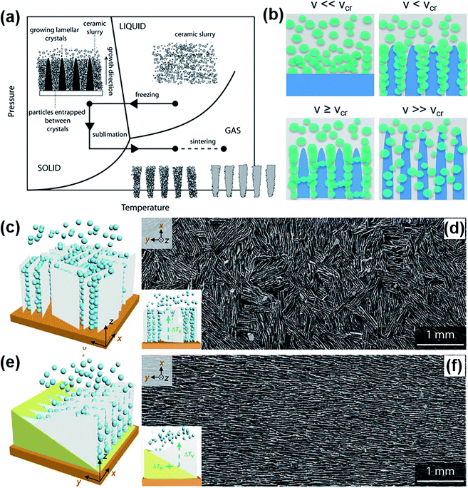 |
| | Fig. 17 Controlled oriented microstructures by freeze casting. (a) Schematic illustration of the four processing steps of the freeze casting technique including slurry preparation, solidification, sublimation and post-treatment. Reproduced from ref. 240 with permission from John Wiley and Sons. (b) Schematic representation of the freezing front progression at different velocities. Reproduced from ref. 49 with permission from John Wiley and Sons. The freezing front progression is decided by the particle freezing front velocity (v) and the ice critical freezing front velocity (vcr). (c and d) Scheme and obtained hydroxyapatite (HA) scaffold of unidirectional freezing casting with a single vertical temperature gradient (ΔTV). (e and f) Scheme of bidirectional freeze casting and the resulting HA scaffold with both the horizontal temperature gradient (ΔTH) and vertical gradient (ΔTV). Reproduced from ref. 242 with permission from the American Association for the Advancement of Science. | |
3.4.4 Chemical vapor deposition (CVD).
Chemical Vapor Deposition (CVD) is a widely used technique that involves a gaseous material reaction and subsequent solid deposition on a substrate. As a versatile bottom-up growth method to synthesize oriented 2D nanomaterials, the obtained material morphology and alignment can be tuned by controlling the growth parameters such as selective source materials, temperature, pressure, gas flow rate and so on.247 The CVD fabrication method is classified as an arbitrary alignment technique here because 2D nanomaterials can be formed into several types of alignment, typically including horizontal, vertical and heterogeneous alignment structures.55,248–253 The alignment of the grown 2D nanomaterials such as TMDCs can be tuned using different CVD growth conditions. Dumcenco et al. reported the morphological changes of MoS2 by tuning the sample temperature.254 When the gas injection temperature gradually decreased from 700 °C to 600 °C, the MoS2 domains went through the vertically aligned multilayers to a reduced longitudinal length, and finally changed into horizontally aligned monolayers. Cho and co-workers fabricated MoS2 films with different alignment directions by rapid sulfurization of CVD (Fig. 18a–d).55 The growth direction of the TMDC films could be controlled by the thickness of the pre-deposited metal seed layer.55,248,251 Horizontal (Fig. 18e), a mixture of horizontal and vertical (Fig. 18f), and vertical alignment (Fig. 18g) were achieved with increasing seed layer thickness. Later, Kumar et al. investigated the horizontal to vertical growth of MoS2 films by tailoring the supersaturation ratio of the S:MoO3 precursors.249 These various aligned structures obtained from direct growth by CVD indicate the possibility to better control the 2D nanomaterials. At the same time, CVD is a scalable method to fabricate diverse nanomaterials with high quality, which requires precise control over the grow parameters.
 |
| | Fig. 18 Controlled orientation of 2D MoS2 films by CVD growth. (a and b) Mo seed layers are predeposited on a substrate. (c) Growth of MoS2 films from horizontal to vertical alignment upon increasing the Mo seed layer thickness. (d) Deposition of an Au/Ti electrode for application. (e) Horizontal layer alignment from 1 nm seed thickness. (f) Horizontal and vertical heterogeneous alignment from 5 nm seed thickness. (g) Vertical film alignment grown from 15 nm seed layer thickness. Reprinted with permission from ref. 55. Copyright (2015) American Chemical Society. | |
In summary, the alignment of 2D nanomaterials can be well controlled through various processing methods involving self-driven or directed assembly. Based on the desired material and target orientation patterns required for specific properties and applications, people can select appropriate fabrication techniques. Furthermore, the selection of the most adequate fabrication process to achieve a target microstructure should also consider (i) the available material quantity and form. For example, all processes except CVD and hydrothermal and gelation require a well-disperse, stable dispersion of 2D nanosheets in a medium; (ii) the intended final relative density. For example, porous structures can easily be formed using freeze-casting, salt templating, or gel casting, whereas hot pressing or vacuum filtration, among others, lead to dense films; (iii) the intended properties and chemistry of 2D nanomaterials. Indeed, the processes requiring chemical reactions or intrinsic properties like anisotropic electric responses are chemically dependent, whereas others are mostly based on the physical properties of the nanosheets such as their dimensions, like magnetic fields, freeze-casting, filtration, etc. Furthermore, the methods reviewed here are representative of the most commonly used methods and have numerous variations in the literature. Although some can produce bulk samples, couple several materials or have heterogeneous alignment patterns, one common limitation of these methods is their inability so far, to decouple the final material shape with the local microstructure. This limits the potential for design and the fabrication of complex structures with tailored, local orientations. Also, in view of creating a multifunctional device containing particles of various chemistries, it is necessary to use a fabrication method that would be efficient independently of the material type. The freedom of shape, orientation, and composition is one of the many advantages that could be brought about by 3D printing. One recent and extremely exciting process with industrial potential is 3D printing. In the following section, how 3D printing can support the microstructure control using 2D nanomaterials is reviewed. The ability to create 3D shapes with locally controlled orientation of 2D nanomaterials in dense or porous packings would allow more design flexibility, giving a bright future for energy devices and others with boosted performances.
4. 2D nanomaterial alignment supported by 3D printing
Substantial efforts have been made to develop various processing techniques to achieve controlled orientations of 2D materials. To implement these achievements into a functional device with enhanced performance, a realistic 3D object or prototype is highly demanded. However, it is challenging to translate the exceptional properties of 2D materials into end structures for specific applications, because it involves assembling and upscaling the oriented microstructure for target properties. For example, it may be necessary to add a layer of glue between components processed separately, preventing intimate bonding between the functional parts and decrease in properties. In this area, 3D printing is a potential solution under the spotlight and a few reviews discuss about the 3D printing of 2D nanomaterials.256,257 However, these reviews miss the importance of 2D nanomaterial alignment and how the combination of 3D printing with alignment could further induce new and enhanced functionalities. In the following section, we therefore review 2D nanomaterial alignment supported by 3D printing and discuss how 3D printing can be expected to fabricate realistic devices with high performance and/or new functionalities.
4.1 Advances in 3D printing
3D printing, or interchangeably called additive manufacturing (AM), refers to the fabrication process of building a 3D structure in a layer-by-layer manner. This fabrication strategy allows customizable computer-aided design (CAD) and precise control of complex patterns from printable inks, for example, containing 2D nanosheets distributed in a matrix. One remarkable advantage of 3D printing over most conventional fabrication processes is the large design freedom. Indeed, the starting materials, 3D printing equipment, final structures, complexity, dimensions, and postprocessing methods can be tailored as desired. As a result, development in the field grows rapidly and has attracted increasing attention from both scientific and industrial communities in the latest decade. 3D printing also allows the fabrication of complex, hierarchical structures with as much diversity as found in biological materials such as those shown in Fig. 1. 2D nanomaterials can therefore be integrated into nano-, micro-, and macroscopic structures, as illustrated in Fig. 19. If some of the common processes have numerous advantages for specific applications, for example for producing homogeneous coatings, fast production of thin films, nearly defect-free 2D nanomaterials, etc., 3D printing technologies open the avenue for the design and fabrication of materials, using one single method, but for potentially any application. More specifically, when it comes to 2D nanomaterial assembly, 3D printing technology reveals unique advantages over the standard processes in the following aspects: (i) local microstructures: the embedded particles can be locally reoriented during the printing process or post-processing, with or without the assistance of external forces such as magnetic, electrical, or acoustic fields. (ii) Multimaterial structures: heterogeneous material compositions can be combined and fabricated synchronously during printing. (iii) Complex shapes: benefiting from the layer-by-layer printing manner, complexity and diversity of the shapes can be broadened, especially for those with hollow structures and intricate interconnections. (iv) Scale up: the dimensions and defined geometries of the printed architectures can be easily customized, enabling the fabrication of scalable products. The 3D printing methods used for 2D nanomaterials are presented in the following section.
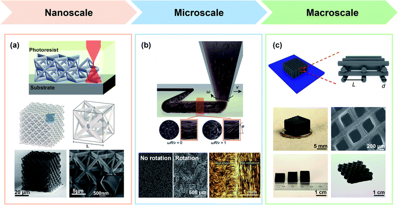 |
| | Fig. 19 Integration of materials into nanoscale, microscale and macroscale structures by 3D printing. (a) Fabrication of nano-sized hollow-tube alumina ceramic nanolattices using two-photon lithography. Reproduced from ref. 258 with permission from the American Association for the Advancement of Science. (b) Carbon fiber orientation during printing through rotational direct ink writing with fiber alignment controllable on a micro-scale. Reproduced from ref. 259 with permission from the National Academy of Science. The helical pattern is dictated by the rotational rate (ω), translational velocity (v), surface fiber orientation (φ) and dimensionless rotation rate (ωR/v). (c) 3D printed graphene aerogel microlattices with various structures and dimensions up to the centimeter scale. Reproduced from ref. 260 with permission from Springer Nature. | |
4.2 3D printing combined with alignment
First described in the 1980s by Charles Hull regarding the stereolithography (SLA) process, 3D printing technology has evolved into multiple printing forms such as inkjet printing, direct ink writing, powder bed fusion, selective laser sintering and so on.261–268 Overall, 3D printing techniques can mainly be classified into three types based on the material feedstock: slurry-based, powder-based and bulk solid-based. Each printing method possesses its own technical features in terms of the equipment setup, feedstock material requirement, and printing advantages and limitations. The recent progress in 3D printing has been summarized in a few comprehensive reviews.262–264,268–271 A few studies report the use of fused deposition modelling (FDM) using graphene but the fabrication of thermoplastic filaments with homogeneously distributed 2D nanosheets is challenging.272,273 In FDM, a thermoplastic filament is heated and extruded through a nozzle on a substrate, where it cools down to solidify. Inkjet printing has also been applied to 2D nanomaterial liquid suspensions but yields horizontal alignment.274 Obtaining vertically oriented nanosheets is difficult due to the capillary forces that develop during solvent evaporation in the deposited droplets. One recent paper reported on the drop-on-demand of purposely oriented 2D nanomaterials by adding a magnetic field. The success of the method depended on the concentration of particles in the ink deposited.275 Moreover, SLA has also been used with 2D nanomaterials.276,277 In SLA, a liquid suspension containing 2D nanosheets and a UV-curable liquid is locally cured using UV light. Using local, sequential curing, SLA has been successfully applied in conjunction with magnetic fields to locally orient 2D nanosheets.278 Also, in SLA, graphene could be horizontally oriented simply by gravitational force during printing.279
Furthermore, the orientation of 2D nanomaterials has been achieved by combining 3D printing techniques with an external magnetic field, electric field and temperature gradient, to introduce particle alignment in a programmable fashion.226,280 Martin et al. utilized the 3D magnetic printing method to fabricate complex oriented architectures using anisotropic 2D particles.281 The particles were oriented and patterned during printing using magnetic fields, where a digital light processor was used to cure the resin (Fig. 20a1–a3). Furthermore, applying a temperature gradient by freeze casting is also a feasible way to create desirable alignment in 3D printing.49 Zhang et al. developed the freeze casting assisted 3D printing of graphene aerogels from a drop-on-demand inkjet printer (Fig. 20b1–b4).282 Freeze casting provides rapid freezing and can manipulate the dispersed graphene orientation along the freezing direction. Thanks to the anisotropic ice crystal growth, the low viscous Newtonian graphene suspension can be printed into highly ordered assemblies as the graphene nanosheets are squeezed between the ice crystals. The printed graphene aerogel obtained presented ultralight densities with high compressibility, demonstrating excellent mechanical robustness. At the same time, the graphene macroscopic material with an aligned microstructure offers high electrical conductivity and potential anisotropic thermal insulation properties for future applications.
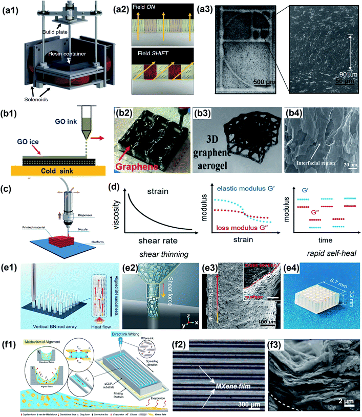 |
| | Fig. 20 Representative 3D printing techniques combined with 2D material alignment. (a1) Schematic representation of the 3D magnetic-printer setup. (a2) The 3D magnetic printing process with programmable magnetic field shift and selective polymerization. (a3) The printed micro-architectures showing complex particle orientation. Reproduced from ref. 281 with permission from Springer Nature. (b1) Schematic of freeze casting assisted 3D printing of graphene aerogel. (b2) 3D printing of graphene suspension. (b3) Thermally reduced 3D ultralight graphene aerogel. (b4) Cross-sectional SEM image showing the interfacial region along the deposition direction. Reproduced from ref. 282 with permission from John Wiley and Sons. (c) Schematic diagram of direct ink writing (DIW). Reproduced from ref. 298 with permission from the Royal Society of Chemistry. (d) Favored rheological properties of a typical DIW ink with shear thinning and rapid self-healing properties. Reproduced from ref. 287 with permission from John Wiley and Sons. (e1) Schematic illustration of the 3D vertical printing of a BN array through the DIW method. (e2) Schematic illustration of BNNS alignment by shear force from the fine nozzle during extrusion. (e3) Morphology of the printed BN rod showing vertically aligned BNNSs. (e4) Scalable BN array encapsulated into a PDMS matrix. Reprinted with permission from ref. 294. Copyright (2019) American Chemical Society. (f1) Schematic of the Ti3C2Tx MXene alignment by capillarity-driven DIW via microcontinuous liquid interface production (μCLIP). (f2) Representative top view of deposited MXene films on patterned substrates. (f3) Printed MXene films showing the alignment. Reprinted with permission from ref. 295. Copyright (2021) American Chemical Society. | |
The direct ink writing (DIW) 3D printing method is preferred for 2D nanomaterials given its ability to print from homogeneously dispersed liquid suspensions. In the following paragraphs, we discuss the DIW method applied to slurries containing 2D nanomaterials, showing multiple orientation control. DIW is an extrusion-based 3D printing technique. In this process, 2D nanosheets are first homogeneously dispersed in a liquid polymer or solvent to produce an ink. As shown in Fig. 20c, the as-prepared ink is extruded from a printing nozzle as a continuous filament, and deposited in a layer-by-layer manner following a predefined pattern, just as directly “writing”.268,283,284 Then, the printed filaments are consolidated by curing under heat or light, other chemical reactions, dried or frozen, depending on the matrix composition used in the ink. As the quality of final printed parts is entirely determined by the rheological properties of the ink, a wide range of 2D nanomaterials can be obtained. Pastes, solutions, and hydrogels have been shown to be printable using DIW.267,285,286 Obtaining appropriate rheological properties for the ink is paramount for successful printing, which is closely related to the filler concentration. To secure this printability, the ink has to exhibit the following key properties (Fig. 20d): shear thinning and viscoelasticity. Indeed, extrusion requires reasonably low viscosity of the ink. Thus, a viscosity decreasing with the applied shear rate is necessary. A viscosity ranging from 0.1 to 103 Pa s−1 is recommended to get smooth printing.269,283,287 In addition, the ink should have viscoelasticity to guarantee shape-retention and stability of the printed part. The elastic (or storage) modulus (G′) should be lower than the loss modulus (G′′) under shear, but should rapidly recover to the opposite (G′ > G′′) once the shear force is removed.288 The behavior of such a viscous ink flow is usually described by the Herschel–Bulkley model:289
where
τ is the shear stress,
τy is the yield stress,
K is the viscosity parameter,
γ is the shear rate, and
n is the shear shinning exponent (
n < 1). In this model, the yield stress is the minimum shear stress above which the ink flows. In the case of a shear stress lower than the yield stress, the fluid behaves like a solid material.
290–292
Having described the DIW printing method, we report how DIW has been used for 2D nanomaterial alignment. The 2D nanosheets dispersed in the ink can be manipulated by external forces or driven by self-assembly when the ink is still liquid, in the barrel, during extrusion, or in the printed parts and before consolidation by post-processing. The ability to locally control the orientation can in turn tune the local properties within the whole 3D part. For example, for 2D nanomaterials with a considerable aspect ratio, the alignment can be induced by shear force along the printing direction.293,294 Liang et al. proposed a general method to fabricate vertically aligned 2D materials on a multiscale by DIW.294 As shown in Fig. 20e1 and e2, the orientation of 2D BNNSs could be induced by the high shear force generated during the extrusion of the ink. As a result, the 2D BNNSs were assembled along the vertical direction, which demonstrated outstanding thermal conductivity in the out-of-plane direction (Fig. 20e3). This shear force assisted printing strategy has been expanded to other 2D nanomaterials such as graphene and MoS2 and can also be upscaled into macroscopic arrays (Fig. 20e4). In addition, Jambhulkar et al. demonstrated the orientation of 2D MXene nanoparticles by capillarity-driven DIW.295 In this case, a patterned substrate with microchannels was fabricated before printing, into which a MXene/ethanol suspension was spread (Fig. 20f1). The high capillary forces generated at the entry of the microchannels overcome the gravity, leading to the flow of MXenes in the microchannels. The Reynolds number, Re, is an index used to describe fluid flow and is key in this process.
| |  | (7) |
where
ρ is the fluid density,
ν is the fluid velocity,
L is the characteristic linear length, and
μ is the viscosity of the fluid. A low
Re (
Re ≪ 1) indicates a laminar flow within the microchannels and is suggested to be the main driving force to MXene nanosheet alignment retained after the subsequent evaporation of the solvent (
Fig. 20f2 and f3).
295–297
In summary, DIW is a highly tunable method that further expands the already large freedom degree of 3D printing by providing alignment control. This permits concomitant design of the shape and of the properties. Indeed, by providing a 3D shape with intricate microstructural features and design capabilities, these methods will enable us to make one step forward towards functional devices using 2D nanomaterials. One limitation however is the concentration of 2D nanosheets in the final material that is limited by the rheological properties. Indeed, it is known that increasing the concentration of nanoparticles leads to jamming of suspensions. In the case of anisotropic nanosheets of a high aspect ratio, this concentration is further decreased. Other points of improvement in DIW are interfilament binding that might compromise the performances of the 3D part, and nanosheet deformation which might reduce their intrinsic properties. Nevertheless, performing 3D objects can now be obtained and tested for real applications.
4.3 Beyond alignment control
The capability of harnessing local structures using 3D printing has potential for developing advanced materials and multifunctional devices. Indeed, we have seen in Section 2 of this review how orienting 2D materials into specific directions could enhance the performance of various functional devices. But the potential of 3D printing goes beyond its capability to create 3D shapes and controlling the local particle orientation. In view of creating multifunctional devices, another benefit of 3D printing is that inks of various chemical compositions can be printed in the same part. This is referred to as multimaterial 3D printing. This could for example lead to the fabrication of devices where the sensor is integrated in a device along with a battery or a supercapacitor, so as to release energy upon a specific external stimulus. It could also be used simply to create compact devices while maintaining low weight, to reduce the volume and payload for automobile or aerospace applications. In addition to this, 3D printed parts with a local orientation and composition can induce new properties in the object, which result from the microstructural control and not entirely from the intrinsic properties of the filler. The most obvious of these new properties is self-shaping. 3D printing with time-varying morphing or performance variations is referred to as 4D printing. With the local orientational and compositional control, it is therefore possible to talk about 6D printing.299 These aspects are reviewed and discussed in the following sections for the specific case of 2D nanomaterials.
4.3.1 Multimaterial fabrication.
Recent advances in 3D printing have revealed the possibility of multimaterial fabrication. Thanks to this unique capability, 3D printing is no longer limited to shaping and offers a broader imagination space for design and multifunctionality. Multimateriality in devices is thought as a means to increase sustainability thanks to the reduction of processing steps, waste material, and increase in functionalities within a small volume.284 For example, Kokkinis et al. established multimaterial magnetically assisted DIW with alumina platelet orientation.300 The DIW printer was equipped with individual syringes and a two-component dispenser to extrude different compositions during printing combined with local control over the building blocks (Fig. 21a). The inks, containing magnetized alumina platelets with fumed silica in resin (Fig. 21b and c), were designed to have printable rheological behaviors. The subsequent control of particle alignment was achieved by applying an external rotating magnetic field before consolidation (Fig. 21d). As a result, the printed macrostructure could be programmed with heterogeneous microstructures through locally tailored particle orientation and multimaterial compositions, as shown in Fig. 21e–g. Moreover, Skylar-Scott et al. achieved soft matter assembly by multimaterial multinozzle DIW.301 The ideal DIW system for multimaterial 3D printing possesses multiple printheads that extrude filaments of various compositions at a sufficiently high switching frequency between the compositions. The multimaterial nozzle can print different compositions within a single continuous filament, a pattern of filaments, or different parts in a macrostructure, which further broadens the design and manufacturing of complex motifs. Hardin et al. also demonstrated multimaterial 3D printing by developing a multimaterial microfluidic printhead for DIW.302 The microfluidic printhead design enabled printing multiple materials from the same nozzle in a seamlessly switching manner. This programmable multimaterial fabrication method demonstrates the chances for building architectures with encoded local compositions for multifunctional applications. Some issues still remain, such as local mixing between the different compositions, which can lead to desired or undesired compositional gradients. Also, interfacial bonding between the different inks is important to be maintained throughout the processing stages to prevent the delamination of the macrostructure at a later stage. More recently, the concept of introducing complex gradient design is implemented in multimaterial 3D printing to reduce the interface mismatches in heterogeneous materials. With a gradient structure, the local mechanical properties of printed products can be altered to prevent the premature failure of devices, for example, to relieve the stress concentration.321 The point of interfacial bonding is rather challenging when anisotropic, local orientations are added to it because of the anisotropic shrinkage that occurs due to temperature or curing, or other discrepancies between each material within the multimaterial composition. These challenges could be mitigated by using inks suspending 2D nanoparticles of various chemistries within the same matrix, and by consolidated the parts via methods that do not use temperature, curing, or drying. In addition, the gradient 3D printing provides the capability of better manipulating local material compositions from functionally graded materials (FGMs) where the material properties can vary spatially in 3D space, shedding light on wider design space and optimized functions in 3D printing.322
 |
| | Fig. 21 Possibility beyond 3D printing with multimaterial fabrication and shape morphing. (a) Schematic of the direct ink writing setup for multimaterial magnetically assisted 3D printing. (b) SEM image of fumed silica particles as a rheology modifier. (c) SEM image of alumina platelets as a functional component. (d) Alignment dynamics of alumina platelets under a rotating magnetic field. (e) Printed macroscopic structure with an internal helicoidal staircase. (f) Morphology of the bottom layer showing effective printing of domains with different local platelet orientations. (g) Printed key-lock structure before and after swelling shape change. Reproduced from ref. 300 with permission from Springer Nature. (h) Schematic of 4D direct ink writing for shear-induced alignment of cellulose fibrils with isotropic, unidirectional, and patterned microstructures. (i) Printed flower morphology changes during the swelling process generated with 90°/0° and 45°/45° bilayer orientation. (j) Print path and (k) printed swollen structure. Reproduced from ref. 314 with permission from Springer Nature. | |
4.3.2 4D printing.
The concept of 4D printing was initially established by Tibbits in 2013.303 4D printing allows the time-dependent evolution of the 3D printed shape or properties by intentionally encoding this time dependence into the part through the 3D printing process.269,270,304–307 Generally, the time-dependent change is triggered by an internal or external stimulus, such as temperature, magnetic field, electric field, particle orientation and pressure.228,308–313 For example, one typical strategy to encode shape change in a 3D printed object is by orienting nanofillers in perpendicular directions in a bilayer and using a matrix that changes its volume in response to an external stimulus. One illustration of such a shape change has been realized by 3D printing anisotropic cellulose fibrils in a soft acrylamide matrix.314 During printing, the cellulose fibrils within the hydrogel composite align due to the shear force (Fig. 21h). Therefore, the printed object had anisotropic elastic and swelling properties tailored thanks to the local control of the filler orientation, which leads to its morphing under hydration (Fig. 21i–k).
In summary, the rapid development of 3D printing technologies has the potential to further unlock the advantages of 2D nanomaterials from the nanoscale to the microscale and up to the macroscale. 3D printing can be efficiently combined with deliberate local 2D nanosheet orientations, multimaterial compositions and time-dependent properties. The capability of controlling local compositions and microstructural alignment in 3D parts of defined shapes could therefore allow the development of new advanced, smart and multifunctional devices. The following section discusses what could be the anticipated exciting prospects and what challenges still need to be faced to this aim.
5. Anticipated prospects and remaining challenges
The aforementioned processing techniques demonstrate the potential of harnessing 2D nanomaterial alignment into desirable assembly patterns, where the local orientation can be horizontal, vertical, heterogeneous, or purposely set in any orientation. Furthermore, 3D printing technologies enable upscaling with the possibility of using multiple local compositions or microstructural orientations. We have seen in Section 2 of this review that oriented 2D nanomaterials significantly boost the performance of sensing, thermoelectric and electrochemical devices. Given all these advances in manufacturing and local orientation and composition, we have to pose the question of how can these advances be leveraged for realistic, smart, multifunctional applications? What remains to be investigated or what could be the difficulties to overcome? These open questions are discussed in the following.
5.1 Anticipated prospects
3D printing of 2D nanomaterials already can create 3D shapes with local design, composition and time-dependent properties. 3D printing can even be further augmented with tunable density by controlling the porosity within the printed filaments in DIW, by adding a sacrificial porogen or a foaming agent, for example. Intentionally introducing nano- or micro-porosity could increase the surface area, contribute to efficient molecule transportation and diffusion, to further augment the functional properties. Therefore, appropriate addition of porosity could lead to objects with a lighter weight but similar, if not increased, performance. This would result in the use of less material feedstock and in turn allow less waste material generation. Another advantage of controlled local porosity, orientation, and composition is the ability to design entirely hierarchical structures from the nanoscopic scale to the macroscopic scale, in a fashion that can be paralleled with the natural materials discussed in Fig. 1 in the Introduction of this review. Hierarchical designs are indeed known to enhance simultaneously the functional and structural properties of natural materials by inducing microstructure-related mechanisms. One common example of hierarchical design is the helicoidal arrangement of nanoparticles in the so-called Bouligand structure in the Mantis shrimp, that provides strength and toughness, while nanochannels spread throughout the material allowing ion flow.315 One could imagine such a similar structure where the nanoparticles in the natural structure are replaced with vertically oriented 2D nanosheets. In this case it could be that the resulting materials could exhibit lower tortuosity, leading to the functionalities reported in Section 2 of this review, in combination to high mechanical performance. The dual presence of enhanced functional and structural properties is important in all devices. Indeed, in operation, devices also need to withstand loads, shocks, vibrations, stresses, etc.
Furthermore, local microstructural design capability also opens up new applications. One could imagine conformable batteries or supercapacitors with complex intricate shapes that integrate inside or around the apparatus to which they supply energy. To maintain the performance in curved designs, for example, the microstructure should be adapted accordingly. One could be interested in this capability when designing compact devices of a high surface to volume ratio and low weight. These kinds of demands are interesting in autonomous vehicles, portable biomedical devices and other robotic applications, for example. Finally, the multimaterial capability of 3D printing would permit the design of multiple devices integrated within one 3D object. Fig. 22 illustrates the design of a multifunctional smart device. Within one 3D device, multiple functionalities can be fused and cooperate automatically, for example, sensing an external heat stimulus, and then generating electrical energy from the waste heat through a thermoelectric module, and later harvesting the electrical energy by using a battery or a supercapacitor. To add more customizable functions, the individual devices could be simply printed next to each other using one unique process, thereby reducing time, manpower, and space for their fabrication. The devices could also be integrated more intimately at a smaller scale, nano or micro, so that their functions are related to each other. Other concrete examples of this concept might be a battery that changes shape depending on an external stimulus and that in turn changes its battery performance, or a supercapacitor with an integrated sensor able to inform on the status of the capacitor or to change its performance depending on external parameters. Materials with embodied and interacting functions are referred to as ‘robotic materials’ and could unlock numerous opportunities for passive actuation of functional device and material computation.316
 |
| | Fig. 22 Schematic illustration of smart functional device design with customizable multifunctionality. | |
The blooming studies on the synthesis and assembly processing of 2D nanomaterials in the past few decades have triggered explosive progress in this research community and brought about great opportunities in diverse application fields. Introducing alignment and designed microstructural patterns with 2D nanomaterials has shown unpredictable capabilities to further amplify the functionalities. Established, state-of-the-art advances demonstrate indeed the great potential of orientated 2D materials in future functional designs and applications. Although these developments lead to exciting, anticipated ideas, a number of challenges remain. Some of these challenges are now discussed.
5.2 Remaining challenges
The first challenge to realize the anticipated prospects is the obtention of a scalable material feedstock of high quality. In terms of 2D nanomaterial synthesis, the current nanomaterials produced through top-down exfoliation and bottom-to-up growth still have a yield far from what is needed for industrial application or commercialization. Furthermore, the quality of the produced 2D nanomaterials is greatly affected by the fabrication methods. For example, mechanical processes may lead to wrinkling of the nanosheets, reducing their properties in the plane. At the same time, chemical processes use harsh chemicals and solvents that are not sustainable or safe, for which waste management and cost are demanding. The synthesis of 2D nanomaterials also determines their dimensions, anisotropy, surface functionalization capability, etc. The 2D nanomaterial quality, composition, size, etc., greatly affect their nanoscopic intrinsic properties. Hence, managing high material quality and quantity are essential for good performances. To achieve high yield and quality, and limit the use of solvents and waste chemicals, biosynthesis and green synthesis should be further explored. Promising results have been obtained for the biosynthesis of graphene using biomolecules,317 and green synthesis of graphene via electrochemical processes,318 and should be transposed for other 2D nanomaterials.
Furthermore, to achieve ideal tunability and high performance of devices based on 2D nanomaterials oriented in multiple directions, it is necessary to unravel the related microstructure–property relationships. The complex relationships between the intrinsic material properties, defects, assembled structure, orientation degree, and connectivity are indeed intrinsically related to the final performances. For example, giving a specific application, suitable material selection, high material quality and a controlled defect level can bring about higher chances for desirable material performances. Moreover, the assembly strategy plays a critical role in further deciding how the final performances are yielded. With better understanding of the internal interactions, 2D nanomaterials could then be rationally modified and arranged into favorable structures using the advanced processing methods or printing technologies described in this review. Computation modelling and simulations, for example using density-functional theory (DFT) modelling, Monte-Carlo simulations and other computation methods should be further used to explore and understand the mechanisms at the nanoscopic and microscopic scales and enable hierarchical design.
Finally, the grand challenge as well as ultimate goal of designing oriented 2D nanomaterials locally and in 3D macrostructures is to leverage their exceptional properties for multifunctional devices. We have seen how 3D printing with local orientational control could open up the design capabilities by provide at least 6 degrees of freedom. How to make best use of such a large design space for target properties? How to open up all the possibilities to find among the best microstructure, composition, local orientation and so forth for realizing the highest performance? These are challenging questions to address which could be tackled with the establishment of open access databases, machine learning and artificial intelligence as well as smart reverse engineering optimization methods.
6. Conclusions
The emerging development of 2D nanomaterials such as graphene, BNNSs, MXenes, TMDCs, etc. sheds light on promising future applications. Controlled local orientation of 2D nanomaterials plays an increasingly important role in realizing high performances for multiple applications. In this paper, we first reported several examples that demonstrate the advantages of orienting 2D nanomaterials in specific directions for enhancing the performance of sensing, thermoelectric and electrochemical devices. We then systematically reviewed the state-of-the-art processing methods to induce controlled alignment of 2D nanomaterials in a desired manner, namely with horizontal, vertical, heterogeneous and arbitrary orientation. Recent advances in 3D printing techniques were then discussed and highlighted the possibility of upscaling 2D nanomaterial assembly from nano- to macro-scales, while further opening other advantages such as multimaterial fabrication and programmable time-dependent evolution. Although 2D nanomaterials with delicately designed local orientations have demonstrated their potential for inducing higher material performances in multiple functional applications, there are multiple challenges to overcome to really create the next generation of devices. We suggested enthusiastic future prospects in this research field as well as pinpointed a few challenges to solve to realize them. From the rapid development of 2D nanomaterials and orientation assembly technology, we can see the great potential in the currently established functional applications and a future breakthrough in harnessing the complexity and multifunctionality.
Author contributions
Hongying He: writing – original draft and conceptualization. Hortense Le Ferrand: conceptualization, supervision, writing – review and editing. Lizhi Guan: writing – review and editing.
Conflicts of interest
There are no conflicts to declare.
Acknowledgements
This research was supported by the National Research Foundation, Singapore under its National Research Foundation Fellowship scheme (award NRFF12-2020-0002).
References
- K. S. Novoselov, A. K. Geim, S. V. Morozov, D.-e. Jiang, Y. Zhang, S. V. Dubonos, I. V. Grigorieva and A. A. Firsov, Science, 2004, 306, 666–669 CrossRef CAS PubMed.
- K. S. Novoselov, A. K. Geim, S. V. Morozov, D. Jiang, M. I. Katsnelson, I. Grigorieva, S. Dubonos and A. A. Firsov, Nature, 2005, 438, 197–200 CrossRef CAS PubMed.
- P. Blake, E. Hill, A. Castro Neto, K. Novoselov, D. Jiang, R. Yang, T. Booth and A. Geim, Appl. Phys. Lett., 2007, 91, 063124 CrossRef.
- D. Akinwande, C. J. Brennan, J. S. Bunch, P. Egberts, J. R. Felts, H. Gao, R. Huang, J.-S. Kim, T. Li and Y. Li, Extreme Mech. Lett., 2017, 13, 42–77 CrossRef.
- S. Z. Butler, S. M. Hollen, L. Cao, Y. Cui, J. A. Gupta, H. R. Gutiérrez, T. F. Heinz, S. S. Hong, J. Huang and A. F. Ismach, ACS Nano, 2013, 7, 2898–2926 CrossRef CAS PubMed.
- Q. H. Wang, K. Kalantar-Zadeh, A. Kis, J. N. Coleman and M. S. Strano, Nat. Nanotechnol., 2012, 7, 699–712 CrossRef CAS PubMed.
- P. Sun, K. Wang and H. Zhu, Adv. Mater., 2016, 28, 2287–2310 CrossRef CAS PubMed.
- R. Mas-Balleste, C. Gomez-Navarro, J. Gomez-Herrero and F. Zamora, Nanoscale, 2011, 3, 20–30 RSC.
- J. Tang and Y. Yamauchi, Nat. Chem., 2016, 8, 638–639 CrossRef CAS PubMed.
- Y. Peng, Y. S. Li, Y. J. Ban, H. Jin, W. M. Jiao, X. L. Liu and W. S. Yang, Science, 2014, 346, 1356–1359 CrossRef CAS PubMed.
- Y. Peng, Y. S. Li, Y. J. Ban and W. S. Yang, Angew. Chem., Int. Ed., 2017, 56, 9757–9761 CrossRef CAS PubMed.
- K. S. Novoselov, A. K. Geim, S. V. Morozov, D. Jiang, M. I. Katsnelson, I. Grigorieva, S. Dubonos and a. Firsov, Nature, 2005, 438, 197–200 CrossRef CAS PubMed.
- A. K. Geim, Science, 2009, 324, 1530–1534 CrossRef CAS PubMed.
-
A. K. Geim and K. S. Novoselov, in Nanoscience and technology: a collection of reviews from nature journals, World Scientific, 2010, pp. 11–19 Search PubMed.
- C. Tan, X. Cao, X.-J. Wu, Q. He, J. Yang, X. Zhang, J. Chen, W. Zhao, S. Han and G.-H. Nam, Chem. Rev., 2017, 117, 6225–6331 CrossRef CAS PubMed.
- X. Zhang, Z. C. Lai, C. L. Tan and H. Zhang, Angew. Chem., Int. Ed., 2016, 55, 8816–8838 CrossRef CAS PubMed.
- H. T. Wang, H. T. Yuan, S. S. Hong, Y. B. Li and Y. Cui, Chem. Soc. Rev., 2015, 44, 2664–2680 RSC.
- V. Guerra, C. Wan and T. McNally, Prog. Mater. Sci., 2019, 100, 170–186 CrossRef CAS.
- K. L. Zhang, Y. L. Feng, F. Wang, Z. C. Yang and J. Wang, J. Mater. Chem. C, 2017, 5, 11992–12022 RSC.
- Y. Lin and J. W. Connell, Nanoscale, 2012, 4, 6908–6939 RSC.
- B. Anasori, M. R. Lukatskaya and Y. Gogotsi, Nat. Rev. Mater., 2017, 2, 16098 CrossRef CAS.
- K. Hantanasirisakul and Y. Gogotsi, Adv. Mater., 2018, 30, 1804779 CrossRef PubMed.
- C. Zhang, Y. L. Ma, X. T. Zhang, S. Abdolhosseinzadeh, H. W. Sheng, W. Lan, A. Pakdel, J. Heier and F. Nuesch, Energy Environ. Sci., 2020, 3, 29–55 CAS.
- M. Naguib, M. Kurtoglu, V. Presser, J. Lu, J. Niu, M. Heon, L. Hultman, Y. Gogotsi and M. W. Barsoum, Adv. Mater., 2011, 23, 4248–4253 CrossRef CAS PubMed.
- M. Naguib, V. N. Mochalin, M. W. Barsoum and Y. Gogotsi, Adv. Mater., 2014, 26, 992–1005 CrossRef CAS PubMed.
- N. San Ha and G. Lu, Composites, Part B, 2020, 181, 107496 CrossRef.
- H.-B. Yao, H.-Y. Fang, X.-H. Wang and S.-H. Yu, Chem. Soc. Rev., 2011, 40, 3764–3785 RSC.
- Y. Zhao, Z. Xie, H. Gu, C. Zhu and Z. Gu, Chem. Soc. Rev., 2012, 41, 3297–3317 RSC.
- R. P. Behera and H. Le Ferrand, Matter, 2021, 4, 2831–2849 CrossRef CAS.
- K. Liu and L. Jiang, Nano Today, 2011, 6, 155–175 CrossRef CAS.
- R. L. Antoniou Kourounioti, L. R. Band, J. A. Fozard, A. Hampstead, A. Lovrics, E. Moyroud, S. Vignolini, J. R. King, O. E. Jensen and B. J. Glover, J. R. Soc., Interface, 2013, 10, 20120847 CrossRef.
- H. Wang, Z. Lu, S. Xu, D. Kong, J. J. Cha, G. Zheng, P.-C. Hsu, K. Yan, D. Bradshaw and F. B. Prinz, Proc. Natl. Acad. Sci. U. S. A., 2013, 110, 19701–19706 CrossRef CAS PubMed.
- E. Reyssat and L. Mahadevan, J. R. Soc., Interface, 2009, 6, 951–957 CrossRef CAS PubMed.
- J. Deng, J. Li, P. Chen, X. Fang, X. Sun, Y. Jiang, W. Weng, B. Wang and H. Peng, J. Am. Chem. Soc., 2016, 138, 225–230 CrossRef CAS PubMed.
- D. Dogu, K. Tirak, Z. Candan and O. Unsal, BioResources, 2010, 5, 2640–2663 Search PubMed.
- C. Wang, X. Chen, B. Wang, M. Huang, B. Wang, Y. Jiang and R. S. Ruoff, ACS Nano, 2018, 12, 5816–5825 CrossRef CAS PubMed.
- J. Huang, X. Wang and Z. L. Wang, Nano Lett., 2006, 6, 2325–2331 CrossRef CAS PubMed.
- S. Gong, H. Ni, L. Jiang and Q. Cheng, Mater. Today, 2017, 20, 210–219 CrossRef CAS.
- E. M. Spiesz, D. T. Schmieden, A. M. Grande, K. Liang, J. Schwiedrzik, F. Natalio, J. Michler, S. J. Garcia, M. E. Aubin-Tam and A. S. Meyer, Small, 2019, 15, 1805312 CrossRef PubMed.
- J. Wang, Q. Cheng, L. Lin and L. Jiang, ACS Nano, 2014, 8, 2739–2745 CrossRef CAS PubMed.
- L. Grunenfelder, N. Suksangpanya, C. Salinas, G. Milliron, N. Yaraghi, S. Herrera, K. Evans-Lutterodt, S. Nutt, P. Zavattieri and D. Kisailus, Acta Biomater., 2014, 10, 3997–4008 CrossRef CAS PubMed.
- H. Le Ferrand, F. Bouville, T. P. Niebel and A. R. Studart, Nat. Mater., 2015, 14, 1172–1179 CrossRef CAS PubMed.
- B. Luo, G. Liu and L. Wang, Nanoscale, 2016, 8, 6904–6920 RSC.
- Z. Zhang, C. S. Lee and W. Zhang, Adv. Energy Mater., 2017, 7, 1700678 CrossRef.
- N. A. Yaraghi and D. Kisailus, Annu. Rev. Phys. Chem., 2018, 69, 23–57 CrossRef CAS PubMed.
- M. S. Cao, X. X. Wang, M. Zhang, J. C. Shu, W. Q. Cao, H. J. Yang, X. Y. Fang and J. Yuan, Adv. Funct. Mater., 2019, 29, 1807398 CrossRef.
- B. Xu, S. Qi, M. Jin, X. Cai, L. Lai, Z. Sun, X. Han, Z. Lin, H. Shao and P. Peng, Chin. Chem. Lett., 2019, 30, 2053–2064 CrossRef CAS.
- Q. Huang, S. Ni, M. Jiao, X. Zhong, G. Zhou and H. M. Cheng, Small, 2021, 2007676 CrossRef CAS PubMed.
- G. Shao, D. A. Hanaor, X. Shen and A. Gurlo, Adv. Mater., 2020, 32, 1907176 CrossRef CAS PubMed.
- C. Lei, Z. Xie, K. Wu and Q. Fu, Adv. Mater., 2021, 2103495 CrossRef CAS PubMed.
- Z. Zhang, J. Du, J. Li, X. Huang, T. Kang, C. Zhang, S. Wang, O. O. Ajao, W.-J. Wang and P. Liu, Prog. Polym. Sci., 2021, 101360 CrossRef CAS.
- D. Voiry, A. Mohite and M. Chhowalla, Chem. Soc. Rev., 2015, 44, 2702–2712 RSC.
- R. M. Ronchi, J. T. Arantes and S. F. Santos, Ceram. Int., 2019, 45, 18167–18188 CrossRef CAS.
- B. G. Compton and J. A. Lewis, Adv. Mater., 2014, 26, 5930–5935 CrossRef CAS PubMed.
- S.-Y. Cho, S. J. Kim, Y. Lee, J.-S. Kim, W.-B. Jung, H.-W. Yoo, J. Kim and H.-T. Jung, ACS Nano, 2015, 9, 9314–9321 CrossRef PubMed.
- J. R. Szczech, J. M. Higgins and S. Jin, J. Mater. Chem., 2011, 21, 4037–4055 RSC.
- J. Zhong, W. Sun, Q. Wei, X. Qian, H.-M. Cheng and W. Ren, Nat. Commun., 2018, 9, 1–11 CrossRef CAS PubMed.
- H. Li, J. Hou, T. D. Bennett, J. Liu and Y. Zhang, J. Mater. Chem. A, 2019, 7, 5811–5818 RSC.
- J. Y. Kim, J. Lim, H. M. Jin, B. H. Kim, S. J. Jeong, D. S. Choi, D. J. Li and S. O. Kim, Adv. Mater., 2016, 28, 1591–1596 CrossRef CAS PubMed.
- H. Le Ferrand, S. Bolisetty, A. F. Demirörs, R. Libanori, A. R. Studart and R. Mezzenga, Nat. Commun., 2016, 7, 1–9 Search PubMed.
- J. Zhu, E. Ha, G. Zhao, Y. Zhou, D. Huang, G. Yue, L. Hu, N. Sun, Y. Wang and L. Y. S. Lee, Coord. Chem. Rev., 2017, 352, 306–327 CrossRef CAS.
- H. He, X. Lu, E. Hanc, C. Chen, H. Zhang and L. Lu, J. Mater. Chem. C, 2020, 8, 1494–1516 RSC.
- H. He, X. Lu, M. Li, Y. Wang, Z. Li, Z. Lu and L. Lu, J. Mater. Chem. C, 2020, 8, 2411–2418 RSC.
- H. He, W. Lu, J. A. S. Oh, Z. Li, X. Lu, K. Zeng and L. Lu, ACS Appl. Mater. Interfaces, 2020, 12, 30548–30556 CrossRef CAS PubMed.
- X. Liu, T. Ma, N. Pinna and J. Zhang, Adv. Funct. Mater., 2017, 27, 1702168 CrossRef.
- G. H. Jeong, S. P. Sasikala, T. Yun, G. Y. Lee, W. J. Lee and S. O. Kim, Adv. Mater., 2020, 32, 1907006 CrossRef CAS PubMed.
- L. Zhang, K. Khan, J. Zou, H. Zhang and Y. Li, Adv. Mater. Interfaces, 2019, 6, 1901329 CrossRef.
- D. J. Buckley, N. C. Black, E. G. Castanon, C. Melios, M. Hardman and O. Kazakova, 2D Mater., 2020, 7, 032002 CrossRef CAS.
- M. Long, P. Wang, H. Fang and W. Hu, Adv. Funct. Mater., 2019, 29, 1803807 CrossRef.
- N. Huo and G. Konstantatos, Adv. Mater., 2018, 30, 1801164 CrossRef PubMed.
- J. J. Pyeon, I.-H. Baek, Y. G. Song, G. S. Kim, A.-J. Cho, G.-Y. Lee, J. H. Han, T.-M. Chung, C. S. Hwang and C.-Y. Kang, J. Mater. Chem. C, 2020, 8, 11874–11881 RSC.
- M. A. Islam, H. Li, S. Moon, S. S. Han, H.-S. Chung, J. Ma, C. Yoo, T.-J. Ko, K. H. Oh and Y. Jung, ACS Appl. Mater. Interfaces, 2020, 12, 53174–53183 CrossRef CAS PubMed.
- Z. Li, Y. Liu, D. Guo, J. Guo and Y. Su, Sens. Actuators, B, 2018, 271, 306–310 CrossRef CAS.
- E. Lee, A. VahidMohammadi, Y. S. Yoon, M. Beidaghi and D.-J. Kim, ACS Sens., 2019, 4, 1603–1611 CrossRef CAS PubMed.
- S. J. Kim, H.-J. Koh, C. E. Ren, O. Kwon, K. Maleski, S.-Y. Cho, B. Anasori, C.-K. Kim, Y.-K. Choi and J. Kim, ACS Nano, 2018, 12, 986–993 CrossRef CAS PubMed.
- D. J. Late, T. Doneux and M. Bougouma, Appl. Phys. Lett., 2014, 105, 233103 CrossRef.
- H. Tang, Y. Li, R. Sokolovskij, L. Sacco, H. Zheng, H. Ye, H. Yu, X. Fan, H. Tian and T.-L. Ren, ACS Appl. Mater. Interfaces, 2019, 11, 40850–40859 CrossRef CAS PubMed.
- A. Shokri and N. Salami, Sens. Actuators,
B, 2016, 236, 378–385 CrossRef CAS.
- H. J. Yoon, J. H. Yang, Z. Zhou, S. S. Yang and M. M.-C. Cheng, Sens. Actuators, B, 2011, 157, 310–313 CrossRef CAS.
- W. Yuan and G. Shi, J. Mater. Chem. A, 2013, 1, 10078–10091 RSC.
- L. Kou, T. Frauenheim and C. Chen, J. Phys. Chem. Lett., 2014, 5, 2675–2681 CrossRef CAS PubMed.
- S. Cui, H. Pu, S. A. Wells, Z. Wen, S. Mao, J. Chang, M. C. Hersam and J. Chen, Nat. Commun., 2015, 6, 1–9 Search PubMed.
- T. Pham, G. Li, E. Bekyarova, M. E. Itkis and A. Mulchandani, ACS Nano, 2019, 13, 3196–3205 CrossRef CAS PubMed.
- J.-H. Kim, A. Mirzaei, H. W. Kim and S. S. Kim, Sens. Actuators, B, 2020, 313, 128040 CrossRef CAS.
- K. Rathi and K. Pal, ACS Appl. Mater. Interfaces, 2020, 12, 38365–38375 CrossRef CAS PubMed.
- S. Kanaparthi and S. G. Singh, Mater. Sci. Energy Technol., 2020, 3, 91–96 CAS.
- Z. Jiang, J. Li, H. Aslan, Q. Li, Y. Li, M. Chen, Y. Huang, J. P. Froning, M. Otyepka and R. Zbořil, J. Mater. Chem. A, 2014, 2, 6714–6717 RSC.
- M. S. Dresselhaus, G. Chen, M. Y. Tang, R. Yang, H. Lee, D. Wang, Z. Ren, J. P. Fleurial and P. Gogna, Adv. Mater., 2007, 19, 1043–1053 CrossRef CAS.
-
G. J. Snyder and E. S. Toberer, Materials for sustainable energy: a collection of peer-reviewed research and review articles from Nature Publishing Group, 2011, pp. 101–110 Search PubMed.
- G. J. Snyder and T. S. Ursell, Phys. Rev. Lett., 2003, 91, 148301 CrossRef PubMed.
- Y. Zhou and L. D. Zhao, Adv. Mater., 2017, 29, 1702676 CrossRef PubMed.
- T. G. Novak, K. Kim and S. Jeon, Nanoscale, 2019, 11, 19684–19699 RSC.
-
H. Goldsmid, Thermoelectric refrigeration, Springer, 2013 Search PubMed.
- Y. M. Zuev, W. Chang and P. Kim, Phys. Rev. Lett., 2009, 102, 096807 CrossRef PubMed.
- Y. Xu, Z. Li and W. Duan, Small, 2014, 10, 2182–2199 CrossRef CAS PubMed.
- D. Dragoman and M. Dragoman, Appl. Phys. Lett., 2007, 91, 203116 CrossRef.
- D. Fan, H. Liu, L. Cheng, P. Jiang, J. Shi and X. Tang, Appl. Phys. Lett., 2014, 105, 133113 CrossRef.
- Y. Guo, C. Dun, J. Xu, P. Li, W. Huang, J. Mu, C. Hou, C. A. Hewitt, Q. Zhang and Y. Li, ACS Appl. Mater. Interfaces, 2018, 10, 33316–33321 CrossRef CAS PubMed.
- M. Khazaei, M. Arai, T. Sasaki, M. Estili and Y. Sakka, Phys. Chem. Chem. Phys., 2014, 16, 7841–7849 RSC.
- S. Sarikurt, D. Çakır, M. Keçeli and C. Sevik, Nanoscale, 2018, 10, 8859–8868 RSC.
- H.-C. Chang and C.-H. Chen, CrystEngComm, 2011, 13, 5956–5962 RSC.
- J. Oh, Y. Kim, S. Chung, H. Kim and J. G. Son, Adv. Mater. Interfaces, 2019, 6, 1901333 CrossRef CAS.
- K. Wu, Y. Zhang, F. Gong, D. Liu, C. Lei and Q. Fu, Chem. Eng. J., 2021, 421, 127764 CrossRef CAS.
- T. Zhu, Y. Liu, C. Fu, J. P. Heremans, J. G. Snyder and X. Zhao, Adv. Mater., 2017, 29, 1605884 CrossRef PubMed.
- L. Fu, T. Wang, J. Yu, W. Dai, H. Sun, Z. Liu, R. Sun, N. Jiang, A. Yu and C.-T. Lin, 2D Mater., 2017, 4, 025047 CrossRef.
- X. Peng, L. Peng, C. Wu and Y. Xie, Chem. Soc. Rev., 2014, 43, 3303–3323 RSC.
- R. Rojaee and R. Shahbazian-Yassar, ACS Nano, 2020, 14, 2628–2658 CrossRef CAS PubMed.
- M. Ghidiu, M. R. Lukatskaya, M.-Q. Zhao, Y. Gogotsi and M. W. Barsoum, Nature, 2014, 516, 78–81 CrossRef CAS PubMed.
- M. A. Hope, A. C. Forse, K. J. Griffith, M. R. Lukatskaya, M. Ghidiu, Y. Gogotsi and C. P. Grey, Phys. Chem. Chem. Phys., 2016, 18, 5099–5102 RSC.
- V. Augustyn and Y. Gogotsi, Joule, 2017, 1, 443–452 CrossRef CAS.
- M. R. Lukatskaya, S. Kota, Z. Lin, M.-Q. Zhao, N. Shpigel, M. D. Levi, J. Halim, P.-L. Taberna, M. W. Barsoum, P. Simon and Y. Gogotsi, Nat. Energy, 2017, 2, 17105 CrossRef CAS.
- M. M. Forouzan, M. Wray, L. Robertson and D. R. Wheeler, J. Electrochem. Soc., 2017, 164, A3117–A3130 CrossRef CAS.
- X. Wang, T. Wang, J. Borovilas, X. He, S. Du and Y. Yang, Nano Res., 2019, 12, 2002–2017 CrossRef.
- Y. Liu, Y. Zhu and Y. Cui, Nat. Energy, 2019, 4, 540–550 CrossRef.
- Z. Ju, X. Zhang, J. Wu and G. Yu, Nano Res., 2021, 14, 3562–3575 CrossRef CAS.
- Y. Xia, T. S. Mathis, M.-Q. Zhao, B. Anasori, A. Dang, Z. Zhou, H. Cho, Y. Gogotsi and S. Yang, Nature, 2018, 557, 409–412 CrossRef CAS.
- J. R. Miller, R. Outlaw and B. Holloway, Science, 2010, 329, 1637–1639 CrossRef CAS PubMed.
- Y. Yoon, K. Lee, S. Kwon, S. Seo, H. Yoo, S. Kim, Y. Shin, Y. Park, D. Kim and J.-Y. Choi, ACS Nano, 2014, 8, 4580–4590 CrossRef CAS PubMed.
-
J. Chen, Z. Bo and G. Lu, Vertically-Oriented Graphene, Springer International Publishing, Switzerland, 2015, vol. 10, pp. 978–973, DOI:10.1007/978-3-319-15302-5.
- J. Billaud, F. Bouville, T. Magrini, C. Villevieille and A. R. Studart, Nat. Energy, 2016, 1, 16097 CrossRef CAS.
- H. Chen, A. Pei, J. Wan, D. Lin, R. Vilá, H. Wang, D. Mackanic, H.-G. Steinrück, W. Huang, Y. Li, A. Yang, J. Xie, Y. Wu, H. Wang and Y. Cui, Joule, 2020, 4, 938–952 CrossRef CAS.
- X. Zhang, Z. Ju, L. M. Housel, L. Wang, Y. Zhu, G. Singh, N. Sadique, K. J. Takeuchi, E. S. Takeuchi, A. C. Marschilok and G. Yu, Nano Lett., 2019, 19, 8255–8261 CrossRef CAS PubMed.
- H. Chen, A. Pei, J. Wan, D. Lin, R. Vilá, H. Wang, D. Mackanic, H.-G. Steinrück, W. Huang and Y. Li, Joule, 2020, 4, 938–952 CrossRef CAS.
- Z. Zhao, M. Sun, W. Chen, Y. Liu, L. Zhang, N. Dongfang, Y. Ruan, J. Zhang, P. Wang, L. Dong, Y. Xia and H. Lu, Adv. Funct. Mater., 2019, 29, 1809196 CrossRef.
- R. Amin, B. Delattre, A. P. Tomsia and Y.-M. Chiang, ACS Appl. Energy Mater., 2018, 1, 4976–4981 CrossRef CAS.
- Z. Ju, Y. Zhu, X. Zhang, D. M. Lutz, Z. Fang, K. J. Takeuchi, E. S. Takeuchi, A. C. Marschilok and G. Yu, Chem. Mater., 2020, 32, 1684–1692 CrossRef CAS.
- L. Zhang, M. Zeng, Z. Liu, Q. Ma, Y. Lu, J. Ma and X. Yan, ACS Appl. Energy Mater., 2021, 4, 5590–5598 CrossRef CAS.
- W. Yang, J. J. Byun, J. Yang, F. P. Moissinac, Y. Peng, G. Tontini, R. A. W. Dryfe and S. Barg, Energy Environ. Mater., 2020, 3, 380–388 CrossRef CAS.
- K. W. Putz, O. C. Compton, M. J. Palmeri, S. T. Nguyen and L. C. Brinson, Adv. Funct. Mater., 2010, 20, 3322–3329 CrossRef CAS.
- K. W. Putz, O. C. Compton, C. Segar, Z. An, S. T. Nguyen and L. C. Brinson, ACS Nano, 2011, 5, 6601–6609 CrossRef CAS PubMed.
- K. Wu, J. Fang, J. Ma, R. Huang, S. Chai, F. Chen and Q. Fu, ACS Appl. Mater. Interfaces, 2017, 9, 30035–30045 CrossRef CAS PubMed.
- X. Lin, X. Shen, Q. Zheng, N. Yousefi, L. Ye, Y.-W. Mai and J.-K. Kim, ACS Nano, 2012, 6, 10708–10719 CrossRef CAS PubMed.
- Z. Ling, C. E. Ren, M.-Q. Zhao, J. Yang, J. M. Giammarco, J. Qiu, M. W. Barsoum and Y. Gogotsi, Proc. Natl. Acad. Sci. U. S. A., 2014, 111, 16676–16681 CrossRef CAS PubMed.
- L. Ding, Y. Wei, L. Li, T. Zhang, H. Wang, J. Xue, L.-X. Ding, S. Wang, J. Caro and Y. Gogotsi, Nat. Commun., 2018, 9, 1–7 CrossRef PubMed.
-
A. Buekenhoudt, A. Kovalevsky, J. Luyten, F. Snijkers and L. Giorno, Comprehensive Membrane Science and Engineering, ed. G. L. Enrico, Elsevier, Oxford, 2010, pp. 217–252 Search PubMed.
- B. Dan, G. C. Irvin and M. Pasquali, ACS Nano, 2009, 3, 835–843 CrossRef CAS PubMed.
- A. Akbari, P. Sheath, S. T. Martin, D. B. Shinde, M. Shaibani, P. C. Banerjee, R. Tkacz, D. Bhattacharyya and M. Majumder, Nat. Commun., 2016, 7, 1–12 Search PubMed.
- C. Simari, A. Enotiadis, C. L. Vecchio, V. Baglio, L. Coppola and I. Nicotera, J. Membr. Sci., 2020, 599, 117858 CrossRef CAS.
- Z. Liu, Z. Xu, X. Hu and C. Gao, Macromolecules, 2013, 46, 6931–6941 CrossRef CAS.
- R. Jalili, S. Aminorroaya-Yamini, T. M. Benedetti, S. H. Aboutalebi, Y. Chao, G. G. Wallace and D. L. Officer, Nanoscale, 2016, 8, 16862–16867 RSC.
- Q. Yang, Z. Xu, B. Fang, T. Huang, S. Cai, H. Chen, Y. Liu, K. Gopalsamy, W. Gao and C. Gao, J. Mater. Chem. A, 2017, 5, 22113–22119 RSC.
- S. Seyedin, E. R. S. Yanza and J. M. Razal, J. Mater. Chem. A, 2017, 5, 24076–24082 RSC.
- J. Bohacek, A. Kharicha, A. Ludwig and M. Wu, ISIJ Int., 2014, 54, 266–274 CrossRef CAS.
- Q. Wei, S. Pei, X. Qian, H. Liu, Z. Liu, W. Zhang, T. Zhou, Z. Zhang, X. Zhang and H. M. Cheng, Adv. Mater., 2020, 32, 1907411 CrossRef CAS PubMed.
- H. Li, P. Tang, H. Shen, T. Hu, J. Chen, K. Chen, F. Qi, H. Yang, L. Wen and F. Li, Carbon, 2021, 183, 840–849 CrossRef CAS.
- K. Wu, J. Wang, D. Liu, C. Lei, D. Liu, W. Lei and Q. Fu, Adv. Mater., 2020, 32, 1906939 CrossRef CAS PubMed.
- Z. Zhuang, Q. Peng and Y. Li, Chem. Soc. Rev., 2011, 40, 5492–5513 RSC.
- S. Han, L. Hu, Z. Liang, S. Wageh, A. A. Al-Ghamdi, Y. Chen and X. Fang, Adv. Funct. Mater., 2014, 24, 5719–5727 CrossRef CAS.
- K.-J. Huang, J.-Z. Zhang, G.-W. Shi and Y.-M. Liu, Electrochim. Acta, 2014, 132, 397–403 CrossRef CAS.
- Y. Deng, T. Shang, Z. Wu, Y. Tao, C. Luo, J. Liang, D. Han, R. Lyu, C. Qi and W. Lv, Adv. Mater., 2019, 31, 1902432 CrossRef CAS PubMed.
- Y. Xu, K. Sheng, C. Li and G. Shi, ACS Nano, 2010, 4, 4324–4330 CrossRef CAS PubMed.
- W. Chen and L. Yan, Nanoscale, 2011, 3, 3132–3137 RSC.
-
S.-H. Feng and G.-H. Li, in Modern inorganic synthetic chemistry, Elsevier, 2017, pp. 73–104 Search PubMed.
- W. Shi, S. Song and H. Zhang, Chem. Soc. Rev., 2013, 42, 5714–5743 RSC.
- N. Xu, J. Liang, T. Qian, T. Yang and C. Yan, RSC Adv., 2016, 6, 98581–98587 RSC.
- X. Yang, L. Qiu, C. Cheng, Y. Wu, Z. F. Ma and D. Li, Angew. Chem., Int. Ed., 2011, 50, 7325–7328 CrossRef CAS PubMed.
- D. Li, M. B. Müller, S. Gilje, R. B. Kaner and G. G. Wallace, Nat. Nanotechnol., 2008, 3, 101–105 CrossRef CAS PubMed.
- U. N. Maiti, J. Lim, K. E. Lee, W. J. Lee and S. O. Kim, Adv. Mater., 2014, 26, 615–619 CrossRef CAS PubMed.
- C. Chen, Y. Tan, X. Han, H. Luo, S. Zeng, S. Peng and H. Zhang, J. Eur. Ceram. Soc., 2018, 38, 5615–5619 CrossRef CAS.
- C. Yu, W. Gong, W. Tian, Q. Zhang, Y. Xu, Z. Lin, M. Hu, X. Fan and Y. Yao, Compos. Sci. Technol., 2018, 160, 199–207 CrossRef CAS.
- Y. Zhang, D. Li, X. Tan, B. Zhang, X. Ruan, H. Liu, C. Pan, L. Liao, T. Zhai and Y. Bando, Carbon, 2013, 54, 143–148 CrossRef CAS.
- J. Kang, S. Hwang, J. H. Kim, M. H. Kim, J. Ryu, S. J. Seo, B. H. Hong, M. K. Kim and J.-B. Choi, ACS Nano, 2012, 6, 5360–5365 CrossRef CAS PubMed.
- P. Liu, Z. Jin, G. Katsukis, L. W. Drahushuk, S. Shimizu, C.-J. Shih, E. D. Wetzel, J. K. Taggart-Scarff, B. Qing and K. J. Van Vliet, Science, 2016, 353, 364–367 CrossRef CAS PubMed.
- X. Zhang, K. Wu, Y. Liu, B. Yu, Q. Zhang, F. Chen and Q. Fu, Compos. Sci. Technol., 2019, 175, 135–142 CrossRef CAS.
- A. Pockels, Nature, 1891, 43, 437–439 Search PubMed.
- F. Rice and K. Herzfeld, J. Am. Chem. Soc., 1934, 56, 284–289 CrossRef CAS.
- M. Gleiche, L. F. Chi and H. Fuchs, Nature, 2000, 403, 173–175 CrossRef CAS PubMed.
- F. Kim, L. J. Cote and J. Huang, Adv. Mater., 2010, 22, 1954–1958 CrossRef CAS PubMed.
- H.-L. Nie, X. Dou, Z. Tang, H. D. Jang and J. Huang, J. Am. Chem. Soc., 2015, 137, 10683–10688 CrossRef CAS PubMed.
- J. Huang, A. R. Tao, S. Connor, R. He and P. Yang, Nano Lett., 2006, 6, 524–529 CrossRef CAS PubMed.
- A. R. Tao, J. Huang and P. Yang, Acc. Chem. Res., 2008, 41, 1662–1673 CrossRef CAS PubMed.
- J. Shen, G. Liu, Y. Ji, Q. Liu, L. Cheng, K. Guan, M. Zhang, G. Liu, J. Xiong and J. Yang, Adv. Funct. Mater., 2018, 28, 1801511 CrossRef.
- M. Zhang, K. Guan, Y. Ji, G. Liu, W. Jin and N. Xu, Nat. Commun., 2019, 10, 1–8 CrossRef PubMed.
- M. Jabbari, R. Bulatova, A. Tok, C. Bahl, E. Mitsoulis and J. H. Hattel, Mater. Sci. Eng., C, 2016, 212, 39–61 CrossRef CAS.
- H. Yuan, X. Liu, L. Ma, Z. Yang, H. Wang, J. Wang and S. Yang, Composites, Part A, 2017, 95, 220–228 CrossRef CAS.
- W. G. Chong, J. Q. Huang, Z. L. Xu, X. Qin, X. Wang and J. K. Kim, Adv. Funct. Mater., 2017, 27, 1604815 CrossRef.
- A. Azizi, M. R. Gadinski, Q. Li, M. A. AlSaud, J. Wang, Y. Wang, B. Wang, F. Liu, L. Q. Chen and N. Alem, Adv. Mater., 2017, 29, 1701864 CrossRef PubMed.
- X. Lin, J. Jia, N. Yousefi, X. Shen and J.-K. Kim, J. Mater. Chem. C, 2013, 1, 6869–6877 RSC.
- Q. Zheng, W. H. Ip, X. Lin, N. Yousefi, K. K. Yeung, Z. Li and J.-K. Kim, ACS Nano, 2011, 5, 6039–6051 CrossRef CAS PubMed.
- C. R. Safinya, E. B. Sirota, R. F. Bruinsma, C. Jeppesen, R. J. Plano and L. J. Wenzel, Science, 1993, 261, 588–591 CrossRef CAS PubMed.
- R. Narayan, J. E. Kim, J. Y. Kim, K. E. Lee and S. O. Kim, Adv. Mater., 2016, 28, 3045–3068 CrossRef CAS PubMed.
- J. Mang, S. Kumar and B. Hammouda, Europhys. Lett., 1994, 28, 489 CrossRef CAS.
- S. Pandit, K. Gaska, V. R. Mokkapati, E. Celauro, A. Derouiche, S. Forsberg, M. Svensson, R. Kádár and I. Mijakovic, Small, 2020, 16, 1904756 CrossRef CAS PubMed.
- C. Yang, Q. Li, M. Nie and Q. Wang, Compos. Sci. Technol., 2021, 215, 109034 CrossRef CAS.
- X. Shen, Q. Zheng and J.-K. Kim, Prog. Mater. Sci., 2021, 115, 100708 CrossRef CAS.
- S. Park, S. Ji, Y. Yoon, S. K. Kim, W. Song, S. Myung, J. Lim, H.-K. Jung, S. S. Lee and K.-S. An, Carbon, 2021, 182, 691–699 CrossRef CAS.
- R. Ye, D. K. James and J. M. Tour, Acc. Chem. Res., 2018, 51, 1609–1620 CrossRef CAS PubMed.
- H. Palneedi, J. H. Park, D. Maurya, M. Peddigari, G. T. Hwang, V. Annapureddy, J. W. Kim, J. J. Choi, B. D. Hahn and S. Priya, Adv. Mater., 2018, 30, 1705148 CrossRef PubMed.
- H. Zeng, X. W. Du, S. C. Singh, S. A. Kulinich, S. Yang, J. He and W. Cai, Adv. Funct. Mater., 2012, 22, 1333–1353 CrossRef CAS.
- L. Li, J. Zhang, Y. Wang, F. U. Zaman, Y. Zhang, L. Hou and C. Yuan, InfoMat, 2021, 3(12), 1393–1421 CrossRef CAS.
- F. Ye, D. Chang, A. Ayub, K. Ibrahim, A. Shahin, R. Karimi, S. Wettig, J. Sanderson and K. P. Musselman, Chem. Mater., 2021, 33(12), 4510–4521 CrossRef CAS.
- S. Z. Noby, K. K. Wong, A. Ramadoss, S. Siroky, M. Hagner, K. Boldt and L. Schmidt-Mende, RSC Adv., 2020, 10, 24119–24126 RSC.
- Z.-Y. Ma, Z.-L. Yu, Z.-L. Xu, L.-F. Bu, H.-R. Liu, Y.-B. Zhu, B. Qin, T. Ma, H.-J. Zhan and L. Xu, Matter, 2020, 2, 1270–1282 CrossRef.
- K. Byrappa and T. Adschiri, Prog. Cryst. Growth Charact. Mater., 2007, 53, 117–166 CrossRef CAS.
- M. K. Devaraju and I. Honma, Adv. Energy Mater., 2012, 2, 284–297 CrossRef CAS.
- J. Min, J. Liu, M. Lei, W. Wang, Y. Lu, L. Yang, Q. Yang, G. Liu and N. Su, ACS Appl. Mater. Interfaces, 2016, 8, 780–791 CrossRef CAS PubMed.
- M. P. Thomas, A. Ullah, R. H. Pham, H. Djieutedjeu, J. P. Selegue and B. S. Guiton, Cryst. Growth Des., 2020, 20, 5728–5735 CrossRef CAS.
- I. S. Neira, Y. V. Kolen’ko, O. I. Lebedev, G. Van Tendeloo, H. S. Gupta, F. Guitián and M. Yoshimura, Cryst. Growth Des., 2009, 9, 466–474 CrossRef CAS.
- G. Canu and V. Buscaglia, CrystEngComm, 2017, 19, 3867–3891 RSC.
- G. Ren, M. N. F. Hoque, X. Pan, J. Warzywoda and Z. Fan, J. Mater. Chem. A, 2015, 3, 10787–10794 RSC.
- J. Zhu, K. Sakaushi, G. Clavel, M. Shalom, M. Antonietti and T.-P. Fellinger, J. Am. Chem. Soc., 2015, 137, 5480–5485 CrossRef CAS PubMed.
- Y. Jiao, A. Mukhopadhyay, Y. Ma, L. Yang, A. M. Hafez and H. Zhu, Adv. Energy Mater., 2018, 8, 1702779 CrossRef.
- C. Lee, X. Wei, J. W. Kysar and J. Hone, Science, 2008, 321, 385–388 CrossRef CAS PubMed.
- P. Y. Chen, M. Liu, Z. Wang, R. H. Hurt and I. Y. Wong, Adv. Mater., 2017, 29, 1605096 CrossRef PubMed.
- J. Luo, H. D. Jang, T. Sun, L. Xiao, Z. He, A. P. Katsoulidis, M. G. Kanatzidis, J. M. Gibson and J. Huang, ACS Nano, 2011, 5, 8943–8949 CrossRef CAS PubMed.
- V. M. Pereira, A. C. Neto, H. Liang and L. Mahadevan, Phys. Rev. Lett., 2010, 105, 156603 CrossRef PubMed.
- J. Zang, S. Ryu, N. Pugno, Q. Wang, Q. Tu, M. J. Buehler and X. Zhao, Nat. Mater., 2013, 12, 321–325 CrossRef CAS PubMed.
- Z. Wang, D. Tonderys, S. E. Leggett, E. K. Williams, M. T. Kiani, R. S. Steinberg, Y. Qiu, I. Y. Wong and R. H. Hurt, Carbon, 2016, 97, 14–24 CrossRef CAS PubMed.
- X. Lei, D. Ye, J. Chen, S. Tang, P. Sun, L. Chen, A. Lu, Y. Du and L. Zhang, Chem. Mater., 2019, 31, 10032–10039 CrossRef CAS.
- H. Jiang, D.-Y. Khang, J. Song, Y. Sun, Y. Huang and J. A. Rogers, Proc. Natl. Acad. Sci. U. S. A., 2007, 104, 15607–15612 CrossRef CAS PubMed.
- Y. Wang, R. Yang, Z. Shi, L. Zhang, D. Shi, E. Wang and G. Zhang, ACS Nano, 2011, 5, 3645–3650 CrossRef CAS PubMed.
- J. Chen, X. Huang, B. Sun, Y. Wang, Y. Zhu and P. Jiang, ACS Appl. Mater. Interfaces, 2017, 9, 30909–30917 CrossRef CAS PubMed.
- E. Pomerantseva and Y. Gogotsi, Nat. Energy, 2017, 2, 1–6 Search PubMed.
- S. Srivastava and N. A. Kotov, Acc. Chem. Res., 2008, 41, 1831–1841 CrossRef CAS PubMed.
- P. T. Hammond, AIChE J., 2011, 57, 2928–2940 CrossRef CAS.
- D. W. Lee, T.-K. Hong, D. Kang, J. Lee, M. Heo, J. Y. Kim, B.-S. Kim and H. S. Shin, J. Mater. Chem., 2011, 21, 3438–3442 RSC.
- L. Schmidt-Mende, A. Fechtenkötter, K. Müllen, E. Moons, R. H. Friend and J. D. MacKenzie, Science, 2001, 293, 1119–1122 CrossRef CAS PubMed.
- B. Yao, J. Chen, L. Huang, Q. Zhou and G. Shi, Adv. Mater., 2016, 28, 1623–1629 CrossRef CAS PubMed.
- P. Xiong, B. Sun, N. Sakai, R. Ma, T. Sasaki, S. Wang, J. Zhang and G. Wang, Adv. Mater., 2020, 32, 1902654 CrossRef CAS PubMed.
- J. E. Kim, T. H. Han, S. H. Lee, J. Y. Kim, C. W. Ahn, J. M. Yun and S. O. Kim, Angew. Chem., 2011, 123, 3099–3103 CrossRef.
- F. Lin, G. Yang, C. Niu, Y. Wang, Z. Zhu, H. Luo, C. Dai, D. Mayerich, Y. Hu and J. Hu, Adv. Funct. Mater., 2018, 28, 1805255 CrossRef.
- F. Lin, Z. Zhu, X. Zhou, W. Qiu, C. Niu, J. Hu, K. Dahal, Y. Wang, Z. Zhao and Z. Ren, Adv. Mater., 2017, 29, 1604453 CrossRef PubMed.
- H. Le Ferrand, J. Eur. Ceram. Soc., 2021, 41, 24–37 CrossRef CAS.
- V. Shukla, Mater. Adv., 2020, 1, 3104–3121 RSC.
- R. M. Erb, R. Libanori, N. Rothfuchs and A. R. Studart, Science, 2012, 335, 199–204 CrossRef CAS PubMed.
- H. Le Ferrand, F. Bouville and A. R. Studart, Soft Matter, 2019, 15, 3886–3896 RSC.
-
H. L. Ferrand, 2021, arXiv preprint arXiv:2103.01440.
- F. L. Bargardi, H. Le Ferrand, R. Libanori and A. R. Studart, Nat. Commun., 2016, 7, 1–8 Search PubMed.
- G. Kim and Y. M. Shkel, J. Mater. Res., 2004, 19, 1164–1174 CrossRef CAS.
- G. Kim, Compos. Sci. Technol., 2005, 65, 1728–1735 CrossRef CAS.
- T. Inadomi, S. Ikeda, Y. Okumura, H. Kikuchi and N. Miyamoto, Macromol. Rapid Commun., 2014, 35, 1741–1746 CrossRef CAS PubMed.
- Q. L. Zhu, C. Du, Y. Dai, M. Daab, M. Matejdes, J. Breu, W. Hong, Q. Zheng and Z. L. Wu, Nat. Commun., 2020, 11, 1–11 CrossRef PubMed.
- S. Wu, R. B. Ladani, J. Zhang, E. Bafekrpour, K. Ghorbani, A. P. Mouritz, A. J. Kinloch and C. H. Wang, Carbon, 2015, 94, 607–618 CrossRef CAS.
- S. Kim, J.-S. Oh, M.-G. Kim, W. Jang, M. Wang, Y. Kim, H. W. Seo, Y. C. Kim, J.-H. Lee and Y. Lee, ACS Appl. Mater. Interfaces, 2014, 6, 17647–17653 CrossRef CAS PubMed.
- P. Collini, S. Kota, A. D. Dillon, M. W. Barsoum and A. T. Fafarman, J. Electrochem. Soc., 2017, 164, D573 CrossRef CAS.
- M. Talib, R. Tabassum, Abid, S. S. Islam and P. Mishra, ACS Omega, 2019, 4, 6180–6191 CrossRef CAS PubMed.
- I. Nelson and S. E. Naleway, J. Mater. Res. Technol., 2019, 8, 2372–2385 CrossRef.
- S. Deville, Scr. Mater., 2018, 147, 119–124 CrossRef CAS.
- W. Tang, S. Tang, X. Guan, X. Zhang, Q. Xiang and J. Luo, Adv. Funct. Mater., 2019, 29, 1900648 CrossRef.
- S. Deville, Adv. Eng. Mater., 2008, 10, 155–169 CrossRef CAS.
- H. Zhang, I. Hussain, M. Brust, M. F. Butler, S. P. Rannard and A. I. Cooper, Nat. Mater., 2005, 4, 787–793 CrossRef CAS PubMed.
- H. Bai, Y. Chen, B. Delattre, A. P. Tomsia and R. O. Ritchie, Sci. Adv., 2015, 1, e1500849 CrossRef PubMed.
- Y. Shao, M. F. El-Kady, C. W. Lin, G. Zhu, K. L. Marsh, J. Y. Hwang, Q. Zhang, Y. Li, H. Wang and R. B. Kaner, Adv. Mater., 2016, 28, 6719–6726 CrossRef CAS PubMed.
- R. Bian, G. He, W. Zhi, S. Xiang, T. Wang and D. Cai, J. Mater. Chem. C, 2019, 7, 474–478 RSC.
- M. M. Porter, P. Niksiar and J. McKittrick, J. Am. Ceram. Soc., 2016, 99, 1917–1926 CrossRef CAS.
- Y. Zhang, L. Hu and J. Han, J. Am. Ceram. Soc., 2009, 92, 1874–1876 CrossRef CAS.
- Z. Cai, B. Liu, X. Zou and H.-M. Cheng, Chem. Rev., 2018, 118, 6091–6133 CrossRef CAS PubMed.
- Y. Jung, J. Shen, Y. Liu, J. M. Woods, Y. Sun and J. J. Cha, Nano Lett., 2014, 14, 6842–6849 CrossRef CAS PubMed.
- P. Kumar and B. Viswanath, CrystEngComm, 2017, 19, 5068–5078 RSC.
- Y. Fang, I. S. Merenkov, X. Li, J. Xu, S. Lin, M. L. Kosinova and X. Wang, J. Mater. Chem. A, 2020, 8, 13059–13064 RSC.
- S. S. Han, J. H. Kim, C. Noh, J. H. Kim, E. Ji, J. Kwon, S. M. Yu, T.-J. Ko, E. Okogbue and K. H. Oh, ACS Appl. Mater. Interfaces, 2019, 11, 13598–13607 CrossRef CAS PubMed.
- B. Zheng, Y. Chen, F. Qi, X. Wang, W. Zhang, Y. Li and X. Li, 2D Mater., 2017, 4, 025092 CrossRef.
- N. Choudhary, H. S. Chung, J. H. Kim, C. Noh, M. A. Islam, K. H. Oh, K. Coffey, Y. Jung and Y. Jung, Adv. Mater. Interfaces, 2018, 5, 1800382 CrossRef.
- D. Dumcenco, D. Ovchinnikov, O. L. Sanchez, P. Gillet, D. T. Alexander, S. Lazar, A. Radenovic and A. Kis, 2D Mater., 2015, 2, 044005 CrossRef.
- Y. Wang, J. Li, X. Li, H. Jin, W. Ali, Z. Song and S. Ding, J. Mater. Chem. A, 2022, 10, 699–706 RSC.
- M. Das, R. S. Ambekar, S. K. Panda, S. Chakraborty and C. S. Tiwary, J. Mater. Res., 2021, 36, 4024–4050 CrossRef CAS.
- I. J. Gómez, N. Alegret, A. Dominguez-Alfaro and M. Vázquez Sulleiro, Chemistry, 2021, 3, 1314–1343 CrossRef.
- L. R. Meza, S. Das and J. R. Greer, Science, 2014, 345, 1322–1326 CrossRef CAS PubMed.
- J. R. Raney, B. G. Compton, J. Mueller, T. J. Ober, K. Shea and J. A. Lewis, Proc. Natl. Acad. Sci. U. S. A., 2018, 115, 1198–1203 CrossRef CAS PubMed.
- C. Zhu, T. Y.-J. Han, E. B. Duoss, A. M. Golobic, J. D. Kuntz, C. M. Spadaccini and M. A. Worsley, Nat. Commun., 2015, 6, 1–8 Search PubMed.
-
C. W. Hull, US Pat., Appl., No. 638905, Filed, 1984 Search PubMed.
- T. D. Ngo, A. Kashani, G. Imbalzano, K. T. Nguyen and D. Hui, Composites, Part B, 2018, 143, 172–196 CrossRef CAS.
- Z. Chen, Z. Li, J. Li, C. Liu, C. Lao, Y. Fu, C. Liu, Y. Li, P. Wang and Y. He, J. Eur. Ceram. Soc., 2019, 39, 661–687 CrossRef CAS.
- X. Wang, M. Jiang, Z. Zhou, J. Gou and D. Hui, Composites, Part B, 2017, 110, 442–458 CrossRef CAS.
-
T. Campbell, C. Williams, O. Ivanova and B. Garrett, Technologies, Potential, and Implications of Additive Manufacturing, Atlantic Council, Washington, DC, 2011, vol. 3 Search PubMed.
-
H. Lipson and M. Kurman, Fabricated: The new world of 3D printing, John Wiley & Sons, 2013 Search PubMed.
- H. Le Ferrand, MRS Bull., 2020, 45, 986 CrossRef.
- H. Le Ferrand, Acc. Mater. Res., 2020, 1, 123–125 CrossRef CAS.
- G. Liu, X. Zhang, X. Chen, Y. He, L. Cheng, M. Huo, J. Yin, F. Hao, S. Chen and P. Wang, Mater. Sci. Eng., R, 2021, 100596 CrossRef.
- Y. Zhang, F. Zhang, Z. Yan, Q. Ma, X. Li, Y. Huang and J. A. Rogers, Nat. Rev. Mater., 2017, 2, 1–17 CrossRef CAS.
- H. Le Ferrand, S. Chabi and S. Agarwala, Adv. Intell. Syst., 2020, 2, 1900151 CrossRef.
- S. Dul, L. Fambri and A. Pegoretti, Composites, Part A, 2016, 85, 181–191 CrossRef CAS.
- J. C. Camargo, Á. R. Machado, E. C. Almeida and E. F. M. S. Silva, Int. J. Adv. Manuf. Technol., 2019, 103, 2423–2443 CrossRef.
- T. Carey, S. Cacovich, G. Divitini, J. Ren, A. Mansouri, J. M. Kim, C. Wang, C. Ducati, R. Sordan and F. Torrisi, Nat. Commun., 2017, 8, 1–11 CrossRef CAS PubMed.
- V. H. Y. Chou, W. C. Liu, M. Wittwer, H. Le Ferrand and M. Seita, Acta Mater., 2022, 117798 CrossRef CAS.
- B. Huang, Z. Zhou, L. Wei, Q. Song, W. Yu, Y. Zhou, R. Hu, W. Zhang and C. Lu, Composites, Part B, 2021, 225, 109261 CrossRef CAS.
- J. O. Palaganas, N. B. Palaganas, L. J. I. Ramos and C. P. C. David, ACS Appl. Mater. Interfaces, 2019, 11, 46034–46043 CrossRef CAS PubMed.
- A. Gurijala, R. B. Zando, J. L. Faust, J. R. Barber, L. Zhang and R. M. Erb, Matter, 2020, 2, 1015–1024 CrossRef.
- K. Markandan, I. P. Seetoh and C. Q. Lai, J. Mater. Res., 2021, 36, 4262–4274 CrossRef CAS.
- H. Le Ferrand and A. F. Arrieta, Soft Matter, 2022, 18, 1054–1063 RSC.
- J. J. Martin, B. E. Fiore and R. M. Erb, Nat. Commun., 2015, 6, 1–7 Search PubMed.
- Q. Zhang, F. Zhang, S. P. Medarametla, H. Li, C. Zhou and D. Lin, Small, 2016, 12, 1702–1708 CrossRef CAS PubMed.
- J. A. Lewis, Adv. Funct. Mater., 2006, 16, 2193–2204 CrossRef CAS.
- V. G. Rocha, E. Saiz, I. S. Tirichenko and E. García-Tuñón, J. Mater. Chem. A, 2020, 8, 15646–15657 RSC.
- T. Billiet, M. Vandenhaute, J. Schelfhout, S. Van Vlierberghe and P. Dubruel, Biomaterials, 2012, 33, 6020–6041 CrossRef CAS PubMed.
- S.-z. Guo, X. Yang, M.-C. Heuzey and D. Therriault, Nanoscale, 2015, 7, 6451–6456 RSC.
- L. Li, Q. Lin, M. Tang, A. J. Duncan and C. Ke, Chem.–Eur. J., 2019, 25, 10768–10781 CrossRef CAS PubMed.
- A. M'barki, L. Bocquet and A. Stevenson, Sci. Rep., 2017, 7, 1–10 CrossRef PubMed.
- W. H. Herschel and R. Bulkley, Kolloid-Z., 1926, 39, 291–300 CrossRef.
- A. Saasen and J. D. Ytrehus, Energies, 2020, 13, 5271 CrossRef CAS.
- R. Yang, J. Zhou, C. Yang, L. Qiu and H. Cheng, Adv. Mater. Technol., 2020, 5, 1901066 CrossRef CAS.
- X. Wang and F. Gordaninejad, J. Intell. Mater. Syst. Struct., 1999, 10, 601–608 CrossRef.
- T. Gao, Z. Yang, C. Chen, Y. Li, K. Fu, J. Dai, E. M. Hitz, H. Xie, B. Liu and J. Song, ACS Nano, 2017, 11, 11513–11520 CrossRef CAS PubMed.
- Z. Liang, Y. Pei, C. Chen, B. Jiang, Y. Yao, H. Xie, M. Jiao, G. Chen, T. Li and B. Yang, ACS Nano, 2019, 13, 12653–12661 CrossRef CAS PubMed.
- S. Jambhulkar, S. Liu, P. Vala, W. Xu, D. Ravichandran, Y. Zhu, K. Bi, Q. Nian, X. Chen and K. Song, ACS Nano, 2021, 15, 12057–12068 CrossRef CAS PubMed.
- G. Xin, W. Zhu, Y. Deng, J. Cheng, L. T. Zhang, A. J. Chung, S. De and J. Lian, Nat. Nanotechnol., 2019, 14, 168–175 CrossRef CAS PubMed.
- M. Trebbin, D. Steinhauser, J. Perlich, A. Buffet, S. V. Roth, W. Zimmermann, J. Thiele and S. Förster, Proc. Natl. Acad. Sci. U. S. A., 2013, 110, 6706–6711 CrossRef CAS PubMed.
- A. Ambrosi and M. Pumera, Chem. Soc. Rev., 2016, 45, 2740–2755 RSC.
- S. K. Georgantzinos, G. I. Giannopoulos and P. A. Bakalis, J. Compos. Sci., 2021, 5, 119 CrossRef.
- D. Kokkinis, M. Schaffner and A. R. Studart, Nat. Commun., 2015, 6, 1–10 Search PubMed.
- M. A. Skylar-Scott, J. Mueller, C. W. Visser and J. A. Lewis, Nature, 2019, 575, 330–335 CrossRef CAS PubMed.
- J. O. Hardin, T. J. Ober, A. D. Valentine and J. A. Lewis, Adv. Mater., 2015, 27, 3279–3284 CrossRef CAS PubMed.
-
S. Tibbits, The emergence of “4D printing”, in TED conference, February 2013 Search PubMed.
- M. Zeng and Y. Zhang, J. Mater. Chem. A, 2019, 7, 23301–23336 RSC.
- F. Momeni, X. Liu and J. Ni, Mater. Des., 2017, 122, 42–79 CrossRef CAS.
- X. Kuang, D. J. Roach, J. Wu, C. M. Hamel, Z. Ding, T. Wang, M. L. Dunn and H. J. Qi, Adv. Funct. Mater., 2019, 29, 1805290 CrossRef.
- S. Tibbits, Archt. Des., 2014, 84, 116–121 Search PubMed.
- Y. Guo, Y. Liu, J. Liu, J. Zhao, H. Zhang and Z. Zhang, Composites, Part A, 2020, 135, 105903 CrossRef CAS.
- C. Yuan, D. J. Roach, C. K. Dunn, Q. Mu, X. Kuang, C. M. Yakacki, T. Wang, K. Yu and H. J. Qi, Soft Matter, 2017, 13, 5558–5568 RSC.
- P. Zhu, W. Yang, R. Wang, S. Gao, B. Li and Q. Li, ACS Appl. Mater. Interfaces, 2018, 10, 36435–36442 CrossRef CAS PubMed.
- Y. Kim, H. Yuk, R. Zhao, S. A. Chester and X. Zhao, Nature, 2018, 558, 274–279 CrossRef CAS PubMed.
- A. Chortos, E. Hajiesmaili, J. Morales, D. R. Clarke and J. A. Lewis, Adv. Funct. Mater., 2020, 30, 1907375 CrossRef CAS.
- F. B. Coulter, B. S. Coulter, E. Papastavrou and A. Ianakiev, 3D Print. Addit. Manuf., 2018, 5, 17–28 CrossRef.
- A. S. Gladman, E. A. Matsumoto, R. G. Nuzzo, L. Mahadevan and J. A. Lewis, Nat. Mater., 2016, 15, 413–418 CrossRef PubMed.
- S. Amini, M. Tadayon, J. J. Loke, A. Kumar, D. Kanagavel, H. Le Ferrand, M. Duchamp, M. Raida, R. M. Sobota and L. Chen, Proc. Natl. Acad. Sci. U. S. A., 2019, 116, 8685–8692 CrossRef CAS.
- M. A. McEvoy and N. Correll, Science, 2015, 347, 1261689 CrossRef CAS PubMed.
- J. Wen, B. K. Salunke and B. S. Kim, J. Chem. Technol. Biotechnol., 2017, 92, 1428–1435 CrossRef CAS.
- H.-L. Guo, X.-F. Wang, Q.-Y. Qian, F.-B. Wang and X.-H. Xia, ACS Nano, 2009, 3, 2653–2659 CrossRef CAS PubMed.
- A. F. Demirörs, P. P. Pillai, B. Kowalczyk and B. A. Grzybowski, Nature, 2013, 503, 99–103 CrossRef PubMed.
- F. Li, Z. Zheng, X. Wang, H. Li and Y. Yan, Chem. Eng. J., 2022, 135920 CrossRef CAS.
- D. Kokkinis, F. Bouville and A. R. Studart, Adv. Mater., 2018, 30, 1705808 CrossRef PubMed.
- L. Ren, Z. Song, H. Liu, Q. Han, C. Zhao, B. Derby, Q. Liu and L. Ren, Mater. Des., 2018, 156, 470–479 CrossRef CAS.
- R. M. Hensleigh, H. Cui, J. S. Oakdale, C. Y. Jianchao, P. G. Campbell, E. B. Duoss, C. M. Spadaccini, X. Zheng and M. A. Worsley, Mater. Horiz., 2018, 5, 1035–1041 RSC.
|
| This journal is © The Royal Society of Chemistry 2022 |
Click here to see how this site uses Cookies. View our privacy policy here. 
 Open Access Article
 This Open Access Article is licensed under a Creative Commons Attribution-Non Commercial 3.0 Unported Licence
 a,
Lizhi
Guan
a and
Hortense
Le Ferrand
a,
Lizhi
Guan
a and
Hortense
Le Ferrand