
 Open Access Article
 This Open Access Article is licensed under a Creative Commons Attribution-Non Commercial 3.0 Unported Licence
Perovskite nanocrystals stabilized in metal–organic frameworks for light emission devices
Wanyi
Nie
 *a and
Hsinhan
Tsai
ab
*a and
Hsinhan
Tsai
ab
aCenter for Integrated Nanotechnologies, Los Alamos National Laboratory, USA. E-mail: wanyi@lanl.gov
bDepartment of Chemistry, University of California, Berkeley, USA
First published on 7th June 2022
Abstract
Metal halide perovskite nanocrystals are recent emerging light emitters with high emission quantum yields and wide color tunability from the ultraviolet to near infrared regions. Perovskite nanocrystals have been applied in high-performance optoelectronics such as bright light-emitting diodes, high-resolution X-ray imaging and photo/radiation sensors, and have received wide attention in this field. However, key challenges such as the poor material stability in the ambient environment and the short operational lifetime under external stress such as an electrical field or illumination still hinder the further development of perovskite nanocrystal-based optoelectronics. Recent intriguing works have smartly incorporated perovskite nanocrystals in metal–organic framework (MOF) matrices to stabilize their emission properties. The resulting perovskite–MOF structures are bright light emitters that have enabled a variety of promising applications. This perspective provides an overview of the recent progress in perovskite/MOF heterostructures and their applications in photonic devices. It first introduces the challenges of stabilizing perovskite nanocrystals, and then discusses how perovskite/MOF structures overcome these problems. We then go over the development of photonic devices using perovskite/MOF as light emitters and describe their potential uses in clean energy conversion and sensing applications.
 Wanyi Nie | Wanyi Nie received her PhD from the Dept of Physics, Wake Forest University. She then joined Los Alamos National Laboratory (LANL) as a postdoctoral researcher. Since 2016, she has been employed as a staff scientist at LANL, and is now leading a team working on perovskite materials and optoelectronic devices. At work, she is passionate about experiments. After work, she likes outdoor activities in the beautiful mountains of Los Alamos and she likes to spend time with her lovely cat at home. |
 Hsinhan Tsai | Hsinhan Tsai is currently a post-doctoral associate at UC Berkeley, Chemistry, where he works with Prof. Jeffrey Long on controlling the crystal growth kinetics and nano-morphologies of MOFs for CO2 capture. He received his BS Degree in Chemistry (Fu Jen Catholic University) and MS Degree in Polymer Science (National Taipei University of Technology). He continued his PhD training in Materials Science and Nanoengineering at Rice University under the supervision of Prof. P. M. Ajayan and Prof. J. Lou, focusing on the development of 2D perovskite materials and their structure–function relationship in photovoltaics, LEDs and radiation detector devices. |
1. Introduction
Efficient photonic sources are in extensive demand for applications that have brought significant value to daily life. For example, among the rapidly growing energy demands across the world, lighting accounts for 20% of the total global energy consumption.1 Light-emitting diodes (LEDs), which use a luminescent semiconductor to convert electricity to light with very low heat loss, dramatically reduce the required energy input for bright light emission. LEDs also provide background lighting in displays in consumer electronics to save energy. Beyond lighting applications, finding a bright photonic source is essential to support applications such as optical communications, optical computer processors, and scintillating screens for medical imaging.Metal halide perovskites are recent wonder materials for high-efficiency photovoltaics,2–7 sensitive radiation sensors,8–18 and low-cost LEDs19–25 (Fig. 1). These materials have the general formula ABX3, where A is a cation, B refers to the metal core and X is a halide. Low-dimensional perovskites, such as 2D quantum wells, quantum dots, and nanocrystals, can be fabricated by adding organic ligands or bulky organic halides to confine the structures (Fig. 1a). Low dimensionality introduces quantum and dielectric confinements to the electronic band structure, where generated electron and hole carriers are strongly bonded at room temperature, promoting radiative recombination for light emission. By tuning their dimensions or composition, nano-structured perovskites show near-unity light emission quantum efficiency at room temperature.26 Attractively, perovskites are low-cost materials in which all the ingredients are earth-abundant elements (i.e., lead iodide and organo-halides), and expensive rare earth metal dopants are not always needed in perovskites to activate their light emission.
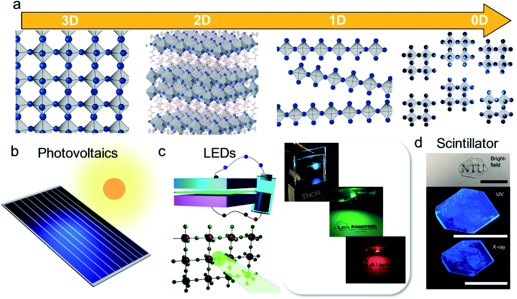 | ||
| Fig. 1 (a) Schematic illustration of the metal halide perovskite structures in 3D, 2D, 1D and 0D. (b) Cartoon illustrations of a perovskite photovoltaic panel. (c) The typical device structure for a perovskite light-emitting diode and photos of perovskite LEDs with tunable colors. (d) Photos of a 2D perovskite crystal that lights up upon UV light (middle panel) and X-ray (lower panel) irradiation. Reproduced from ref. 11 with permission from Springer Nature. | ||
Innovations in the fabrication of perovskite nanocrystals have been extensively reported in recent years. An open scientific problem is the stabilization of luminescent nanocrystals in the ambient environment or during device operation. Recently, an emerging structure by growing perovskite nanocrystals in metal–organic frameworks (MOFs), porous metal–organic matrices used to protect the perovskite nanocrystals, has been shown to achieve bright light emission with extended lifetimes under harsh conditions. Recently, the intriguing properties of perovskite/MOF (PeMOF) materials, in particular their outstanding stability, have been reported27–29 and photonic devices such as light-emitting diodes20,30 and radiation scintillators using PeMOF emitters have also been demonstrated in the past few years. It is noteworthy that a few review articles have comprehensively discussed the various synthetic approaches for PeMOF structures and summarized most of the PeMOF combinations reported in the literature.31–33 Thus, this perspective will not repeat summarizing the reported structures and properties from all aspects, rather we focus on discussing how PeMOF structures can address the challenging problems in perovskite nanocrystal-based photonic devices. Firstly, we introduce the perovskite nanocrystals for light-emitting devices and their instability problems, which must be overcome. Next, we summarize the established mechanisms responsible for the degradation of nanocrystal, and based on these mechanisms, we discuss how can PeMOF structures solve this issue. After summarizing the advances of PeMOF structures, we then review the progress in the use of PeMOFs in photonic devices. In particular, the challenges in making lighting devices and why PeMOFs are feasible to address these challenges will be discussed. Finally, we present an outlook of the future applications of PeMOF-based lighting devices.
1.1 Background of luminescent perovskite nanocrystals
Various methods have been explored for the synthesis of perovskite nanocrystals (Fig. 2). Colloidal perovskite quantum dots are typically grown by introducing a perovskite precursor in a non-coordinating solvent in the presence of a capping ligand such as oleic acid and oleyl amine (Fig. 2a). Tuning the precursor ratio and length of the ligands can control the nanocrystal size. This method results in nanocrystals with a narrow size distribution, usually in a few-nanometer range, with exceptional photoluminescence (PL) quantum efficiencies of over 80%.34,35 All-inorganic CsPbX3 quantum dots with 90% emission yield have been achieved by a newly developed “hot-injection” method.36 Other methods for nanocrystal growth have also been explored. For instance, encapsulating perovskites in a nanoshell also produces highly emissive nanomaterials (Fig. 2b). Perovskites in SiO2 nanoshells have been demonstrated with high luminescent properties. Interestingly, these crystals are bio-compatible, and thus promising for drug delivery.37 Also, a distorted non-perovskite structure such as Cs4PbX6 (ref. 38–40) and CsPb2Br5 (ref. 41–43) is smartly employed to encapsulate an ABX3 perovskite core, e.g., CsPbX3 crystal-forming a core–shell structure.38,40,42,44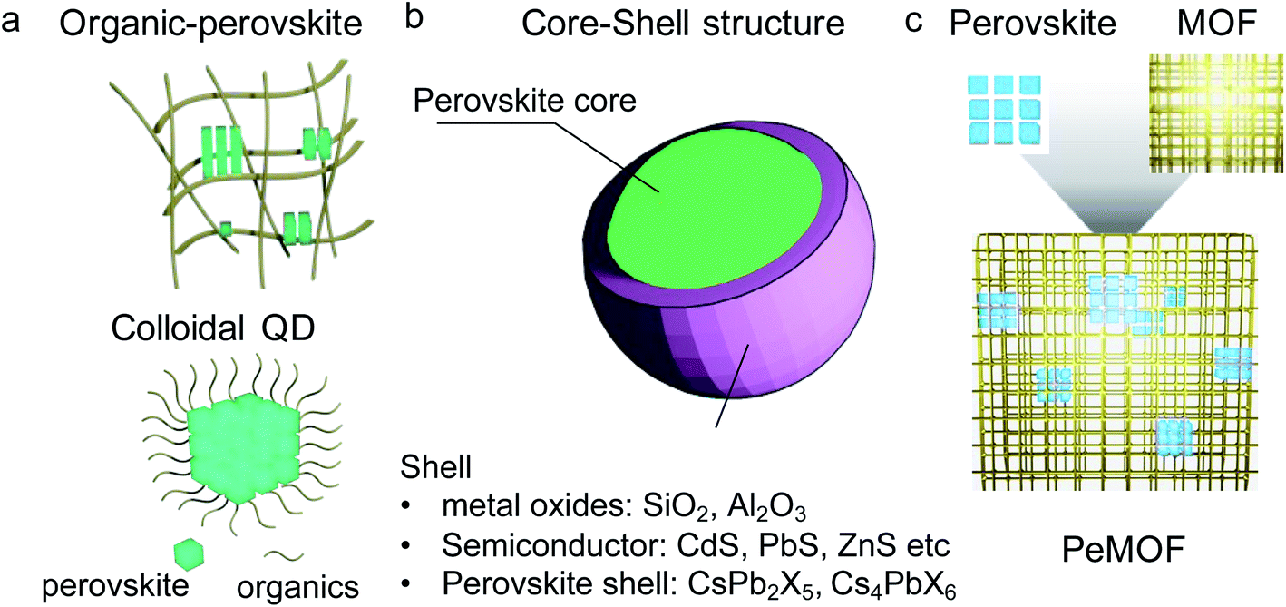 | ||
| Fig. 2 Perovskite nanocrystal developed in the field. Schematic illustration of (a) examples of organic-perovskite nanocrystal structures, (b) core–shell structure to confine the perovskite nanocrystals and (c) perovskite/MOF structure by confining the perovskite nanocrystal in a MOF matrix. | ||
Perovskite nanocrystals can be also confined in an organic matrix or metal–organic framework (Fig. 2c). The presence of the matrix will limit the perovskite crystal growth rate, and thus confine its shape, yielding highly emissive nanostructures. The perovskite/MOF structure will be introduced in detail in the next section.
Nano-structures such as CsPbBr3 quantum dots and 2D perovskite quantum wells have been integrated in photonic devices such as light-emitting diodes,40,45–47 scintillators15,48,49 and lasers.50–52 Uniquely, high-quality thin films can be produced by low-temperature solution-based methods, where printing techniques can be employed for large-scale manufacturing. Because of their high emission yields, LEDs fabricated using perovskite nanocrystals with outstanding electroluminescence quantum efficiencies of over 20% have been demonstrated. Perovskite nanocrystal-based LEDs delivered a high color purity in green23,53,54 and high electroluminescence (EL) of over 10![[thin space (1/6-em)]](https://www.rsc.org/images/entities/char_2009.gif) 000 cd m−2, meeting the industrial requirement of color purity and brightness, respectively.20
000 cd m−2, meeting the industrial requirement of color purity and brightness, respectively.20
1.2 Current challenge in stabilizing nanocrystals and their opto-electronic devices
Currently, one of the main obstacles associated with perovskite nanostructures is their poor stability, where several major degradation mechanisms have been identified. Firstly, nanocrystals are thermodynamically unstable and tend to merge back to the bulk phase, which quenches their emission efficiency. It is shown that perovskite nanocrystals merge to form larger aggregates55 upon heating or even being stored at room temperature, which shifts the peak position and reduces their emission intensity.56 Constant illumination can also age perovskite nanocrystals. Huang et al. found that crystal aggregation occurred under a constant illumination, exhibiting 10-times lower PL than the fresh materials.57 Secondly, similar to bulk perovskite materials, the ambient environment is detrimental to perovskite nanocrystals, where moisture or oxygen can accelerate the decomposition of their structure to the precursor phase. Pioneering works have found that moisture or oxygen can destroy the surface of nanocrystals by electro-chemical reaction, which removes their ligands and quenches their emission.58 Thirdly, external stress such as illumination and electrical field can drive the movement of ions in their structures, which shifts their emission peak position, and ultimately damages the material. It is worth noting that the ion migration effect is a major problem for almost all perovskite-based electronic devices.59 It was first recognized in perovskite photovoltaics, where the sweeping voltage from different polarity causes significant differences in the current–voltage characteristics even in a small voltage range (<2 V).60,61 Later, ion migration was determined to be a more severe problem in perovskite lighting devices, where higher biases (typically greater than 3 V) must be applied for electroluminescence.62,63 Consequently, the emissions of most LEDs decay by 50% within 20 min of continuous operation even under a moderate bias,58 which occurs even faster when driving the device at its maximum brightness. In addition, the ion migration problem also persists in perovskite nanocrystals,64 which is believed to occur near the surface of the crystal where defects are often located. Another challenge is the voltage-induced color instability of perovskite LEDs. Continuous color tunability is usually achieved by tuning the halide composition in the perovskite structure, such as adding iodide to bromide perovskites, which red-shifts their emission color by optical band gap narrowing. However, under an electrical field, the originally well-mixed halides tend to aggregate into individual domains, e.g., bromide-rich vs. iodide-rich domains, shifting the emission color.65 Vashishtha and Halpert66 showed that orange-colored LEDs made with CsPb(BrXI1−X)3 nanocrystals turned green after about 6 min of operation because of the halide segregation. In addition to ion migration, the aforementioned nanocrystal merging problem in thin films and their sensitivity to light and environmental factors further worsen the instability issue. This poor operational stability has hindered the further development of perovskite light-emitting devices, weakening their superior light emission properties.1.3 Strategies to stabilize perovskite nanocrystals
Motivated by these challenges, solving the instability problem becomes one of the core research directions in this field. Based on the mechanisms discussed in Section 1.2, the goal is to find novel structures to (1) effectively separate nanocrystals to avoid their merging in the thin film form, (2) protect the material from external degradation factors such as moisture and oxygen and (3) passivate surface defects to suppress ion migration. Besides the material stability, the operational stability of opto-electronic devices under a constant electrical field or light irradiation also needs to be considered. The electrical field-induced instability is related to the ion migration problems, which is often assisted by defects near the surface. The interface instability caused by the electro-chemical reaction between the perovskites and commonly used metal electrodes is also a severe problem. When an LED lights up, joule heating is inevitable when running a constant current through the device. Therefore, the thermal stability of nanocrystals should be greatly improved for their long-term operation.Recently, considerable efforts have been devoted to stabilizing perovskite nanocrystals in various matrices to protect them from degradation. Accordingly, several structures have been investigated for extending the lifetime of perovskite nanocrystals.
As mentioned in Section 1.1, perovskite–perovskite core–shell structures are also promising structures to stabilize the promising emission properties of NCs. For instance, a distorted CsPb2X5 or Cs4PbX6 shell can be grown on the CsPbX3 core to protect the NCs. Growing similar structures from solution is more straightforward, and the distorted shells have been proven to provide good protection against heat and other environmental factors.40 However, they have some shortcomings, such as the limited choice of distorted structures, and most studies are dedicated to CsPbX3 all-inorganic perovskite NCs.
2. Growing perovskite nanocrystals in MOFs is a promising strategy to stabilize the material
In this section, we summarize the possible mechanisms for the extended stability in PeMOF structures.2.1 Mechanism-1: MOF is a protective shell for perovskite nanocrystals to prevent them from merging
Perovskite nanocrystals can be in situ-grown inside the MOF structure, yielding a finely dispersed heterostructure. The porous structure of MOFs is a well-defined matrix to confine the growth of the crystals, resulting in the formation of ultra-small crystals. The nanocrystals are isolated by the robust MOF matrix, and thus the probability of crystal merging is greatly reduced. Fig. 3 illustrates a few reported TEM images of perovskite nanocrystals grown in MOFs. Perovskite nanocrystals ranging from 20 nm (Fig. 3a) down to 5 nm or smaller (Fig. 3c) were successfully fabricated in the MOF matrix. The emission peak position shown in Fig. 3b is 532 nm for the 10–20 nm crystals and that in Fig. 3d is 527 nm for the 5 nm crystals, exhibiting a small blue-shifted emission compared to the bulk, However, they did not reach the size limit for quantum confinement for a dramatic blue shift. As shown in Fig. 3e and f, very small MAPbI3 dots less than 5 nm in the oriented MOF matrix were achieved by Chen et al.,104 and because of the confinement effect, the emission peak position in PL spectrum of the MAPbI3 dots, as shown in Fig. 3g, blue-shifted by 80 nm compared to that for the bulk MAPbI3, providing a viable route to tune its emission colors. Alternatively, color tunability can be achieved by mixing the halides at the X site (Fig. 4a), as illustrated in Fig. 4b, where bright tunable emissions were demonstrated by Cha et al.105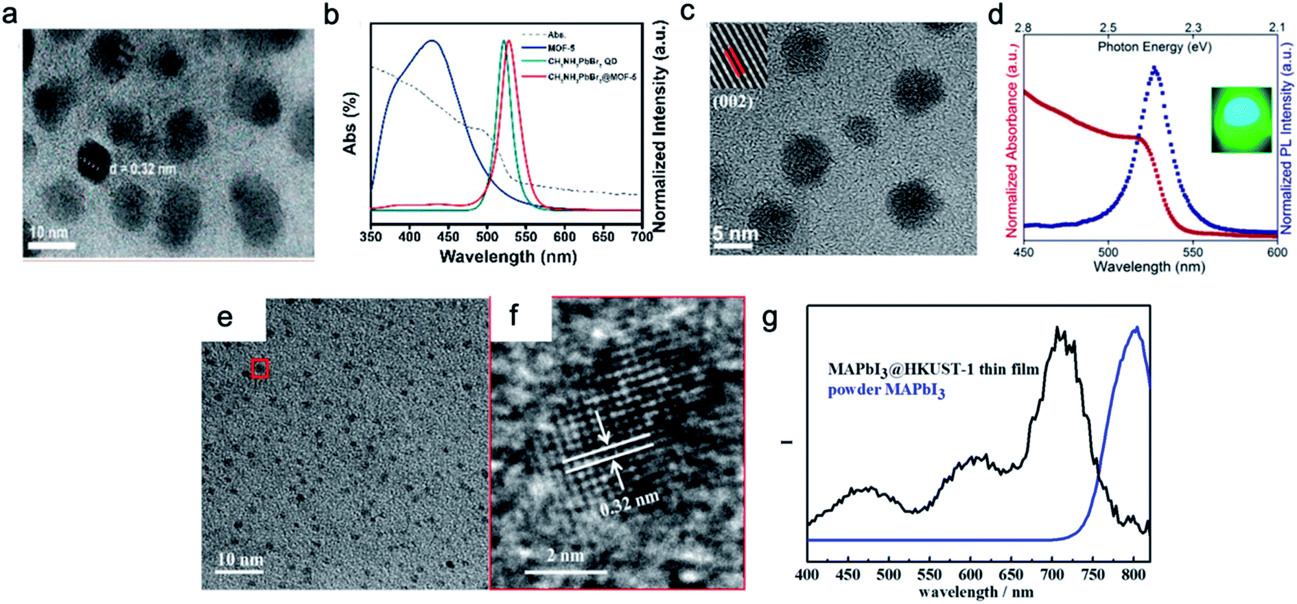 | ||
| Fig. 3 Perovskite nanocrystals grown in the MOF. (a and b) An example of 10–20 nm MAPbBr3 nanocrystals grown in MOF-5 and their UV/PL spectra. Reprinted with permission from ref. 102. Copyright 2018 American Chemical Society. (c and d) An example of ∼5 nm MAPbBr3 crystals grown in the ZIF-8 matrix and their UV/PL spectra. Reprinted with permission from ref. 103. Copyright 2019 American Chemical Society. (e and f) High-resolution TEM images of small perovskite dots grown in Cu-BTC MOF thin films and the typical photoluminescence spectrum for the PeMOF thin film plotted in (g). Reprinted with permission from ref. 104. Copyright 2016 American Chemical Society. | ||
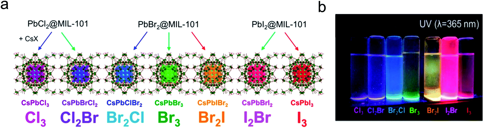 | ||
| Fig. 4 (a) Tunable colors can be achieved by mixing chloride with bromide, or bromide with iodide. (b) Photo of the mixed halide PeMOF nanocrystal suspensions showing different colors under UV irradiation. Reprinted from ref. 105 with permission. Copyright 2019 American Chemical Society. | ||
2.2 Mechanism 2: MOF matrix is a physical barrier to protect perovskite nanocrystals from oxygen and humidity
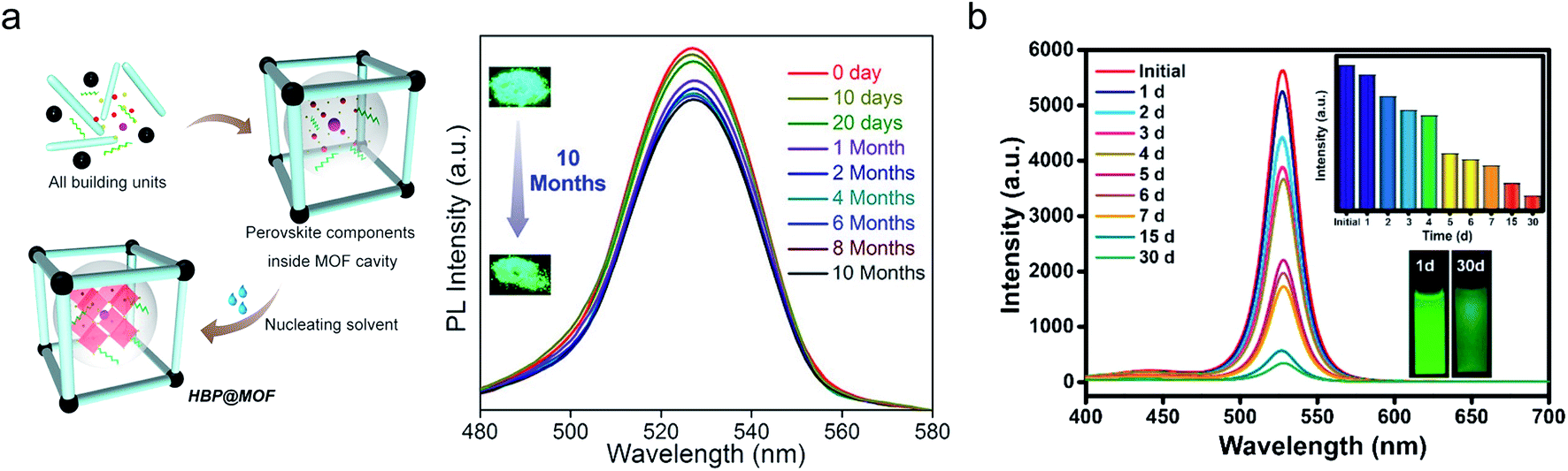
As discussed in Section 1.2, the exposure of perovskite nanocrystals to the ambient environment is detrimental, where moisture or oxygen can accelerate their aging. Because perovskite nanocrystals can be in situ grown in the MOF matrix, the heterostructure is on the nanoscale. Therefore, the MOF matrix can wrap the individual nanocrystals, forming a nano-phase heterostructure to prevent their direct contact with oxygen or moisture. This type of structure is more effective than microscopic composites, such as a mixture of nanocrystals in a polymer.In addition, a hydrophobic MOF matrix can be selected to further repel water from perovskite nanocrystals, allowing the materials to function in a moist environment. For instance, PCN-221(Fex) was used to protect MAPbI3 nanocrystals,106 which could function in an aqueous environment for the carbon dioxide reduction reaction. Similarly, Kong et al. developed a CsPbBr3-ZIF core–shell structure, which exhibited improved moisture stability.107 Water-resistant PeMOFs were also developed for photonic sources. Zhang et al. in situ grew MAPbBr3 nanodots in Zn8(Ad)4(BPDC)6O·2Me2NH2, where Ad refers to adeninate and BPDC is biphenyldicarboxylate, called bio-MOF-1. Bio-MOF-1 had micrometer-sized pores, which could encapsulate the perovskite dots, sustaining the perovskite light emission over 80 days in open air. In contrast, the emission from the bare perovskite sample diminished within 5 min.108 Similarly, as shown in Fig. 5a, Mollick and coworkers assembled MAPbBr3 quantum dots in ZIF-8, a well-known MOF, and tracked their photoluminescence signal over 10 months in the ambient environment, where merely less than 10% degradation was detected.103 Water-stable PeMOF have also been demonstrated by Zhang et al.102 Unprotected perovskites are water soluble and will instantaneously lose their perovskite structure in water. In contrast, the PeMOF developed by Zhang et al. was immersed in water and was still emissive after 30 days (Fig. 5b). Note that moisture has been identified as the key driving force that accelerates the degradations of perovskite materials and devices. For example, the current voltage hysteresis of perovskite photovoltaics and the rapid decay of the perovskite emission are often found to be worsened after exposure to moisture. Therefore, building water-resistant, functional PeMOF heterostructures will be a breakthrough in this field, which can overcome the fundamental challenge in all perovskite-based devices.
 | ||
| Fig. 5 Moisture stability of PeMOF. (a) PeMOF structures developed by Mollick et al., where the emission from the perovskite remains strong over 10 months of air exposure. Reprinted with permission from ref. 103. Copyright 2019 American Chemical Society. (b) Photoluminescence spectra of the PeMOF developed by Zhang et al., which exhibits robust emission when immersed in water for 30 days. Reprinted with permission from ref. 102. Copyright 2018 American Chemical Society. | ||
A recent breakthrough must be mentioned here, where Hou et al. demonstrated ultra-stable inorganic CsPbX3 pure and mixed halide perovskite nanocrystals sealed in a ZIF-62 MOF, i.e., Zn[(Im)1.95(bIm)0.05] (Im, imidazolate and bIm, benzimidazolate).109 Not only bright emissions with tunable colors were shown, the PeMOF crystals exhibited brilliant water resistance, where 80% of their initial PL was maintained after 10000 h in water.
2.3 Mechanism-3: MOF matrix retains the organo-halide salt to retard the water-induced decomposition
Taking organo-halide perovskite as an example, when water diffuses into the perovskite system, chemical decomposition occurs via a reversible reaction route, as follows: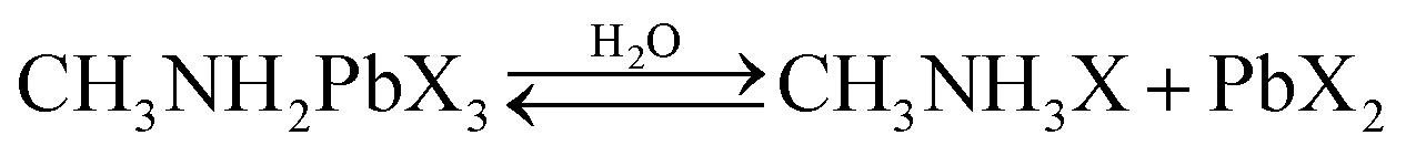 | (1) |
 | (2) |
The decomposition of the perovskite is a reversible process, where it decomposes into its precursors (from left to right), and subsequently can be re-formed from its precursors (from right to left). On the right side of the reaction, if there is a continuous loss of CH3NH3X via reaction (2), then reaction (1) will tend to move towards the right side of the equation towards decomposition. In the PeMOF structure, it is believed that the MOF matrix intimately contacting the nanocrystals can retain CH3NH3X, thus maintaining the reversible reaction (1).110
Besides moisture stability, the long-term stability of nanocrystals in various solvent systems and under constant UV irradiation is important for building reliable devices for displays or white light sources for indoor lighting. Here, the PeMOF maintained 80% of its PL intensity in various solvent environments (Fig. 6a), which suggests the strong solvent resistance due to the MOF protection. In addition, PeMOF structures have been proven to be tolerant to heat and UV irradiation. For instance, the same PeMOF structure demonstrated by Mollick and coworkers also exhibited good stability under constant UV irradiation (Fig. 6b). In particular, the PeMOF could maintain over 80% of its original PL intensity after 20 days of constant UV illumination, indicating that the nanostructures were well maintained in the MOF matrix.
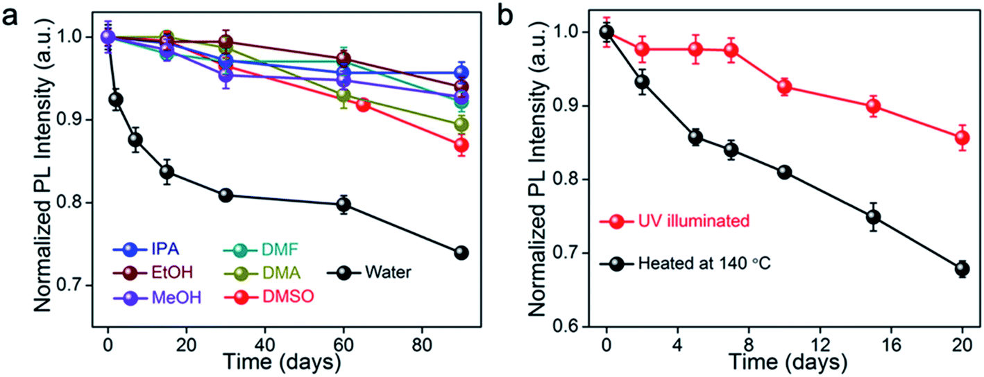 | ||
| Fig. 6 The normalized PL intensity of the PeMOF fabricated by Mollick et al. tested in (a) various solvent systems and (b) over 20 days with heat stress and under constant UV illumination. Reprinted with permission from ref. 103. Copyright 2019 American Chemical Society. | ||
To compare the PeMOF structures and the achieved material stabilities, we summarize the perovskite and MOF material structures, stability test conditions and achieved material lifetimes in Table 1.
| MOF | Perovskite | Stability test conditions | Property monitored for stability and lifetime | Application | Ref. |
|---|---|---|---|---|---|
| Eu-BTC | CsPbBr3 | Thermal cycling from 20 °C to 100 °C | PL peak position remained unchanged after thermal cycling | Temperature sensing | 110 |
| MOF-5 | MAPbBr3 | Thermal cycling from 30 °C to 230 °C | PL intensity retained a linear dependence with temperature after 7 cycles | Metal ion sensing | 102 |
| Expose to water | PL was still observable after 30 days | ||||
| MIL-101 | CsPbX3, X = Cl, Br, I | Ambient air exposure | PL emission intensity for Br3, Br/Cl mixture remained unchanged | Photonic source | 105 |
| ZIF-8 | MAPbBr3 | Immersion in water and various organic solvents | >90% PL emission retained after 90 day exposure to water | Heterogenous photocatalysis | 103 |
| Continuous heating at 140 °C with UV irradiation | >60% PL emission retained after 20 days | ||||
| HP-UiO-66 | CsPbI3 | 400 nm constant photoexcitation for 2 h | A slight decrease (15%) in the initial PL intensity was observed | White LED | 111 |
| Thermal cycling from 25 °C to 100 °C | The PL intensity was maintained at 91% after thermal cycling | ||||
| MOF-5 | CsPbX3 | Thermal stability: heating up to 120 °C | PeMOF preserved 72.8% of its original PL intensity@80 °C | White LED | 112 |
| Photo-stability tested under constant UV (400 nm) irradiation | 71.4% of PL intensity was maintained after 80 hour illumination | ||||
| Dark storage lifetime tested | PeMOF preserved 79.2% of its original PL after 60 days of storage | ||||
| Bio-MOF-1 | MAPbBr3 | Air exposure with constant UV irradiation (365 nm) | PeMOF powder maintained good fluorescence after 90 days of exposure | White LED | 108 |
| UiO-67 | CsPbBr3 | Thermal cycling from 30 °C to 200 °C | 85% of the PL intensity was retained after 9 cycles | White LED | 113 |
| Air exposure | PL emission intensity maintained after 30 days | ||||
| Pb-BTC | MAPbBr3, CsPbBr3 | Constant UV (256 nm) irradiation in air | 90% PL retained after 300 h irradiation | Green LEDs | 20 |
| Electrical current injection at 1.2 mA cm−2 | 50% of the original EL retained after 40 h continuous LED operation | ||||
| Pb-BTC | CsPb(BrCl)3 | Electrical bias stress at 4.2 V | 50% of the original EL retained after 8000 s operation | Blue LED | 30 |
| agZIF-62 | CsPbI3 | Immersion in milli-Q water | 80% PL retained after 105 h of water immersion | Colored and white LEDs | 109 |
According to this summary, four types of stabilities have been achieved in PeMOF structures. Firstly, moisture/water stability. The MOF matrix protects the perovskites from moisture and hydrophobic MOFs such as ag-ZIF-62, ZIF-8 and MOF-5 can repel water, enabling the NCs to function even under water. The second type is thermal stability, where the emission properties of the perovskite NCs are well preserved after several heating/cooling cycles up to 230 °C in the PeMOF structure. The third type of stability is photostability, where PeMOFs were exposed to constant UV irradiation (250 nm–400 nm). The NCs could sustain their emission yield and emission peak positions in MOFs, indicating the nanocrystal sizes were well preserved. This is particularly important when PeMOFs are used as a phosphor layer to produce white LEDs. The final stability tests were conducted under electrical field stress, when the PeMOF was integrated in LEDs. Green and blue LEDs were fabricated, where direct electroluminescence occurred from the PeMOF layer by charge injection. The perovskites in the Pb-BTC MOFs could withstand constant electrical field stress without a change in their peak position. Their emission intensity was also maintained for an extended period. Direct and indirect conversion LEDs will be discussed in detail in Section 4.
3. Perovskite-metal–organic framework structure fabrication mechanisms
To make a PeMOF structure, the MOF structure should be synthesized first. MOFs are porous organic–inorganic crystals, which consist of metal nodes connected by organic linkers, forming a framework. They have been used in diverse applications, including gas and liquid separation, energy storage, drug delivery, sensing and direct CO2 capture. These applications are highly dependent on the surface area and morphology of the crystal, where precise control of the material structure during the crystallization process is essential. Methods such as solvothermal,114,115 sonochemical,116,117 coordinate modulation96,118 are employed to grow MOF crystals from nanoscale to mm-scale single crystals.To growth high-quality PeMOF with a controllable size, optical and electrical properties, several approaches have been developed, which are nicely discussed in a few of review articles.31–33,119 Herein, we use the four categories described in these articles to briefly summarize the fabrication methods for PeMOF heterostructures (Table 2), as follows: (a) ship-in-bottle: this strategy utilizes the pore size of a pre-formed MOF as the host and provides controllable sites and size for perovskite nanocrystal nucleation; (b) bottle around ship: in this technique, the perovskite nanocrystals are synthesized first, and then the MOF precursors assembled in the solution; (c) in situ one-pot synthesis: in this method, the perovskite and MOF precursors are pre-mixed in solution, and simultaneously form a nanocrystal-MOF composite; and (d) in situ conversion: this is a simple approach where an MOF matrix with Pb as the metal node is synthesized first, and then organo-halide salts are introduced in the Pb-MOF for perovskite nanocrystal conversion and growth.20,30,120 The conversion of the perovskite material is normally completed by reacting PbX2 with halide salts at elevated temperature to complete the crystal formation. Here, the Pb-MOF provides the lead source for perovskite conversion, and because of the porous sites in the MOF matrix around the Pb sources, the crystal growth can be limited to the nanoscale.
| Method | MOF | Perovskite | MOF size (nm) | Protection mechanism | Stability | Ref. |
|---|---|---|---|---|---|---|
| Ship-in-bottle | UIO-66 | MAPbBr3 | 0.692 | Preserve PbBr2 in MOF | Reversible emission | 121 |
| UIO-67 | CsPbX3 (Br, I) | 2 | Confine the NC in MOF matrix | Prevent the NCs from merging | 113 | |
| Cu-BTC (HKUST-1) | MAPbX3 (Cl, Br, I) | N/A | Confine the NC in the MOF matrix | Moist air | 104 | |
| Eu-BTC | MAPbBr3 | 0.91 | Preserve PbBr2 in MOF | Reversible emission | 122 | |
| ZIF-8 | MAPbBr3 | N/A | Confined nanostructure | Chemical, photo, thermal | 103 | |
| MIL-101 | CsPbX3 (Cl, Br, I) | 2.9–3.4 | Confine in MOF to avoid halide inter-mixing | Preserved color in ambient air | 105 | |
| MOF-5 | CsPbX3 (Cl, Br, I) | 25 | MOF encapsulates NC | Thermal photo | 112 | |
| AMOF-1 | CsPbX3 (Cl, Br, I) | N/A | Preserve the NC size | Photo | 123 | |
| ZJU-28 | CsPbX3 (Cl, Br, I) | N/A | Separate/passivate NC | Photo | 124 | |
| ZIF-8 | CsPbX3 (Cl, Br, I) | 4 | Large pore allows in situ growth | Photo | 125 | |
| PCN-221(Fex) | MAPbI3 | 1.8 | Hydrophobic linker | Water immersion | 106 | |
| Bottle around ship | Eu-BTC | CsPbBr3 | N/A | Thermal | 110 | |
| ZIF-8 | CsPbBr3 | N/A | MOF is an encapsulation shell | Moisture | 107 | |
| ZIF-67 | CsPbBr3 | N/A | MOF is an encapsulation shell | Moisture | 107 | |
| One pot synthesis | ZIF-62 | CsPbX3 (Cl, Br, I) | N/A | Hydrophobic MOF matrix | Water immersion | 109 |
| MOG | EAPbBr3 | 2.5–10 | MOF encapsulation | Moisture, photo | 126 | |
| In situ conversion | Pb-BTC | CsPbX3 (Cl, Br) | N/A | Confine the NC in matrix | Photo, electrical | 30 |
| Pb-BTC | MAPbX3 (Cl, Br, I) | N/A | Confine the NC in matrix | Photo, electrical | 20 and 120 |
4. Light-emitting devices using PeMOF crystals and thin films
PeMOF structures have been demonstrated in various device applications. Notably, MOFs have been utilized for protecting the perovskite photo-absorbing layer to achieve stable solar cells and employed for capturing lead leakage from photovoltaic devices.27 Most impressively, water-stable PeMOFs have been developed as a photocatalyst for CO2 reduction and hydrogen generation to provide alternative renewable energy sources. More advanced applications such as security ink developed by PeMOF powder have been demonstrated.120 These various applications have been covered in the previously published review articles.31,33 In this section, we focus on perovskite lighting device applications.Because of the strong and robust light emission properties of PeMOF materials, the next step is to develop light-emitting devices to achieve electroluminescence. Two types of LEDs have been investigated using PeMOFs and their simplified structures are illustrated in Fig. 7. Fig. 7a shows a typical indirect conversion type in which a PeMOF layer is coated on a high energy (blue or UV) LED to down-convert photons to visible light. Fig. 7b shows a typical direct conversion-type LED, where the PeMOF layer is directly used as the active emission layer to accept electron/hole injection from the electrodes for EL. However, different challenges exist in these two types of devices, which have to be overcome for their reliable operation, and thus will be introduced in the following sub-sections.
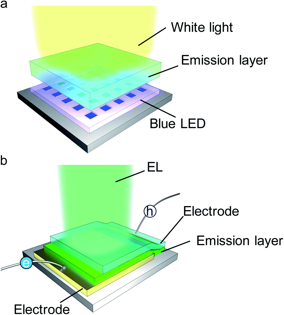 | ||
| Fig. 7 Cartoon illustrations of (a) a down-conversion LED and (b) a direct-conversion LED. | ||
4.1 PeMOF down-conversion layer for white LEDs
A typical down-conversion LED is generally composed of a high-brightness blue LED coated with one or several luminescent materials, where part of the blue light can be re-absorbed and visible photons are re-emitted. This is widely used technology for white indoor lighting and display panels for commercial electronics. White lighting devices are hard to achieve using direct-conversion LEDs because a multi-color emission layer is rarely available and balancing the colors to achieve the required white color appearance (i.e., warm white or cold white) is complicated in this structure. Therefore, down-conversion LEDs are a better choice for white LEDs, in which multiple emission dyes can be layered or mixed to tune the ratio of red-blue-green. Modern QD TVs are made with down-conversion LEDs, where QDs are coated on the backlighting panels to enhance the color output.127 Popular down-conversion materials include rare-earth phosphors, organic dyes and QDs.Here, the key challenge is to achieve stable brightness and tunable emission colors from a phosphor material under constant blue or UV LED irradiation. As mentioned in Section 1.2, perovskite nanocrystals without further protection are detrimental to constant illumination and humidity can accelerate their degradation. UV irradiation can initiate the merging of the nanocrystals, which destroys their emission intensity. Color tuning is normally achieved via halide mixing; however, based on the discussion in Section 1.2, halide segregation can occur under UV light irradiation, which will shift off the emission color. Both problems are unfavorable for building down-conversion devices.
This problem can be addressed using PeMOF materials. Recently, Guan et al. reported a highly luminescent CsPbX3/MOF (X = Br or I) nanostructure with 10%–45% photoluminescence quantum yield.111 In particular, they synthesized a hierarchically porous nanocrystalline MOF and guided the growth of CsPbX3 nanocrystals in the matrix. This PeMOF structure was coated on a commercial GaInN blue LED to assemble a white LED. Impressively, the CsPbX3/MOF delivered a bright emission with a stable spectrum over 72 h of continuous operation, which cannot be achieved with unprotected perovskite nanocrystals. Similarly, Zhang et al. assembled CsPbBr3 QDs in a UiO-67 MOF, which exhibited great thermal stability.113 They mixed the PeMOF with K2SiF6:Mn4+, forming a composite and achieving a white LED, as shown in Fig. 8a. Ren et al. developed a meso-porous MOF to encapsulate all-inorganic perovskite quantum dots, where the MOF formed a shell over the quantum dots, solving the thermal and photo instability issues.112 They fabricated PeMOF powders with bromides (green emission) and mixed halide perovskite crystals (Fig. 8b) and mixed both powders in a polymer binder. By coating this mixture on a blue LED, they built a warm white LED, as shown in Fig. 8c. The previously mentioned MAPbBr3/Bio-MOF-1 structure developed by Zhang et al., which could maintain its emission over 80 days in air, was also integrated with down-conversion LEDs with tunable colors. As illustrated in Fig. 8d, they achieved both a single-colored LED and warm white LED by mixing blue, green and red powders.108
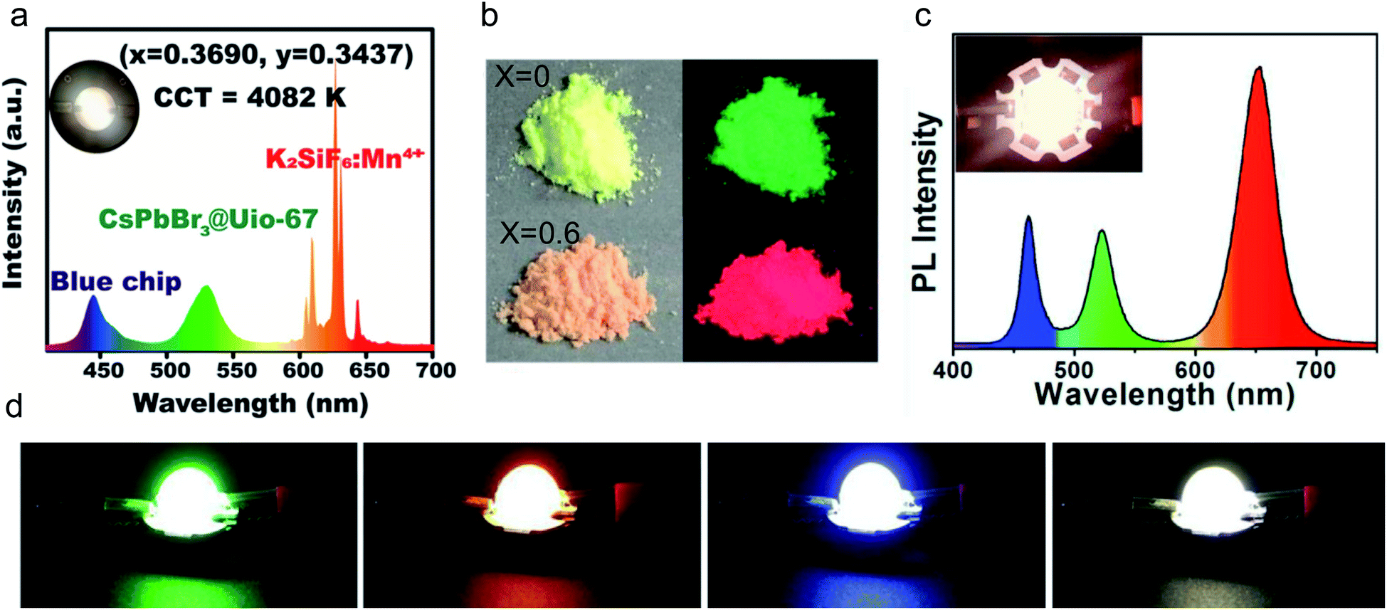 | ||
| Fig. 8 (a) PL spectra of the as-fabricated WLEDs with the CsPbBr3@Uio-67 composite and commercial K2SiF6:Mn4+ red phosphor deposited on the blue chip (InGaN, 455 nm). Inset: Photograph of the WLEDs. (b) Photographs of CsPbI3-xBrx/MOF-5 powders (x = 0 and 0.6) taken under daylight (left) and 365 nm UV illumination (right). Reprinted with permission from ref. 113. Copyright 2019 American Chemical Society. (c) The corresponding EL spectrum with a photo of the white LED in the inset. Reprinted from ref. 112. Copyright 2019, with permission from Elsevier. (d) Photograph of blue, green, red, and white LEDs, respectively, using Bio-MOF-1 developed by Zhang et al. Reprinted from ref. 108. Copyright 2019, with permission from Elsevier. | ||
4.2 PeMOF as the active emission layer for direct electroluminescence
The second type is the use of a PeMOF as the emission layer in an LED, where the EL comes directly from the electron hole recombination in the PeMOF layer by injecting charges from selective electrodes. A typical thin film LED is formed with a thin emission layer sandwiched between an electron injection electrode and a hole injection electrode. To make a high-performance thin film LED, several challenges exist. The first requirement is to find emissive materials with suitable electronic properties. In an ideal LED, electrons and holes are injected and travel at the same rate and recombine in the middle of the emission layer to deliver a high electroluminescence efficiency. Unbalanced charge injection will cause one type of carrier to travel faster than the other, and the faster carrier gets quenched near the interface, reducing the emission yield. Besides the electronic properties, achieving ultra-high uniformity of the emission layer is also critical. The emission layer is normally made to have a lower thickness (20–100 nm), where the surface roughness should be minimized to apply a uniform electrical field across the device. The presence of pinholes or non-uniformity will result in a large shunt current without producing electroluminescence, which diminishes the external quantum efficiency. The third challenge is specific to perovskite materials, where the migration of mobile ions has to be minimized during device operation to avoid a decay in brightness and color instabilities. PeMOF structures have the potential to overcome the third problem according to extensive material stability investigations, while their feasibility for the first and second requirements are unknown.Recently, we reported the preparation of a PeMOF thin film LED for direct-conversion electroluminescence for the first time.20,30 The PeMOF conversion is based on method (d) described in Section 2. Briefly, Pb-MOF was first synthesized,128 where the Pb metal coordinate center in the MOF provides the lead source for the conversion of the perovskite nanocrystal.120 We noticed that the poor solubility of MOF presents a major challenge in coating a high-quality thin film from solution. In our work, we employed a modified two-step method to fabricate a PeMOF thin film, as illustrated in Fig. 9, where in step (1) Pb-MOF is first dispersed in DMSO/HBr, and them the precursor is spin-coated on a substrate to form a thin layer. Here, we noticed that adding a trace amount of hydrobromic acid helped to dissolve the MOF in the organic solvent. In step (2), an MABr (or CsBr, FABr)-containing solution is spin-coated on the Pb-MOF thin film to convert the film into PeMOF. Finally, an annealing step is applied to complete the growth of the nanocrystal, where 8–13 nm crystals are formed in the MOF matrix.
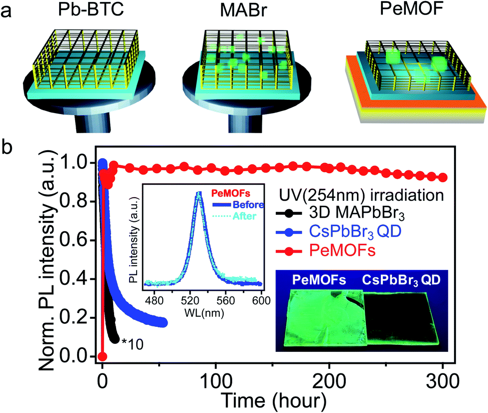 | ||
| Fig. 9 (a) Illustration of the PeMOF thin film fabrication process via a two-step spin coating method. (b) Time evolution of the normalized photoluminescence intensities of the 3D MAPbBr3 thin film, CsPbBr3 QD thin film and PeMOF thin film. The PL spectrum for a PeMOF thin film before and after UV irradiation is plotted in the inset, and a photo of the PeMOF versus QD thin films after aging is shown in the same plot. Reproduced from ref. 20 with permission. | ||
The resulting PeMOF thin film showed durable emission properties under constant UV irradiation. Fig. 9b shows a comparison of the PL intensities of the 3D CsPbBr3 perovskite, commercial CsPbBr3 QD and CsPbBr3 nanocrystal PeMOF thin films under UV lamp irradiation in air. The bulk perovskite film rapidly decayed almost instantaneously, whereas the QD film lost 80% of its PL within 50 h. In contrast, the PeMOF thin film maintained its emission over 300 h and its PL spectrum remained unchanged.
Finally, a direct conversion LED was demonstrated. The device structure is shown in Fig. 10a, where PeMOF is sandwiched between electron and hole injection electrodes for electroluminescence. The average external quantum efficiency, the emitted photons divided by injected electrons, of the PeMOF LED was about 14% (Fig. 10b). Importantly, the device showed much a better operational lifetime. While most of the reported perovskite LEDs decay within 20 min of continuous operation, the PeMOF device was stable over 20 h operation under a low injection current, as shown in Fig. 10c. All-inorganic nanocrystals have also been integrated in the PeMOF structure for LEDs. Recently, our group demonstrated the mixing of Br and Cl halides in CsPbX3 nanoparticles in MOFs to achieve blue colors. Fig. 10d shows the resulting blue PeMOF LEDs, which emitted brightly with sky-blue and deep-blue colors. The external quantum efficiencies for the blue LEDs were as high as 5.6%, as shown in Fig. 10e. Interestingly, by integrating all-inorganic perovskite nanocrystals in MOFs, e.g., CsPbBr3, the resulting lifetime of the LEDs was even longer under a higher injection current. The time evolution of the PeMOF LED EL using Cs-PeMOF as the emission layer is plotted in Fig. 10f, where the half-lifetime (T50) is the time when the device emission decays to 50% of its peak value, was over 50 h. We attributed the better lifetime to the thermal stability of the inorganic perovskite nanocrystals, which is more tolerant to the joule heating induced by constant current injection.
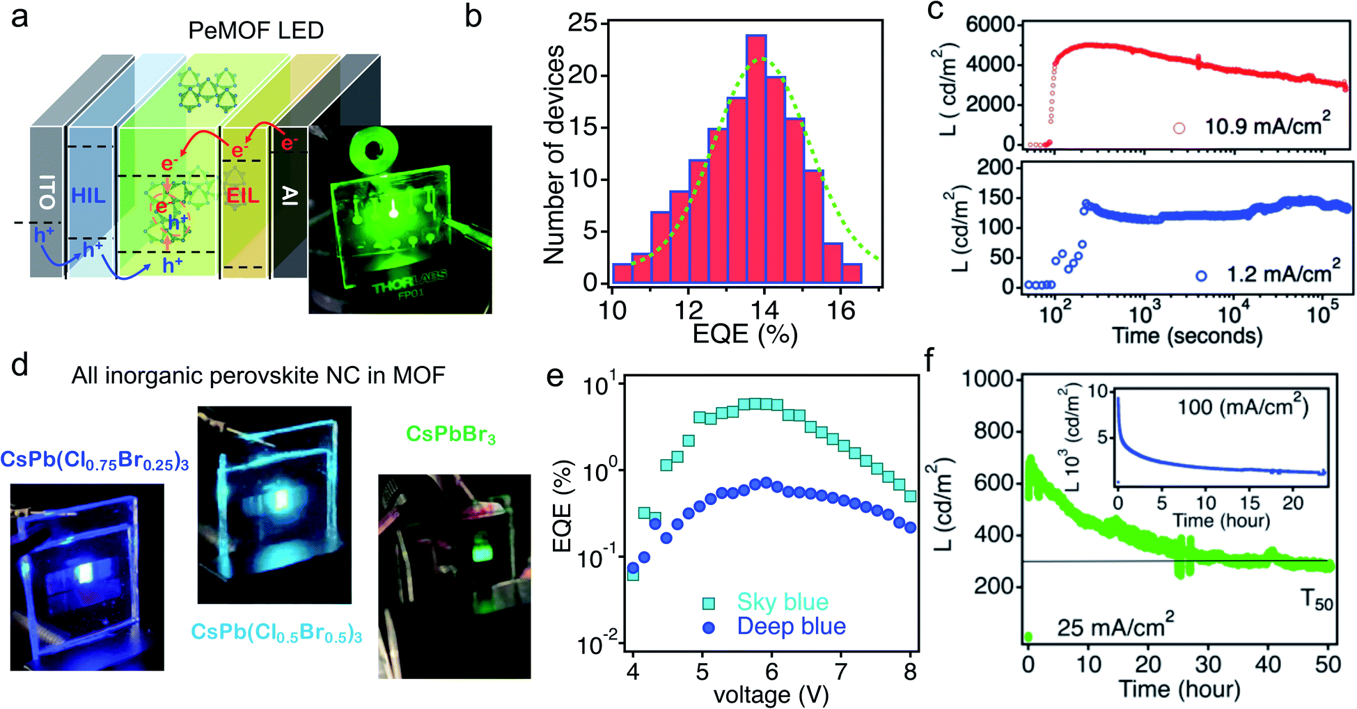 | ||
| Fig. 10 (a) A sketch of the device structure of the PeMOF LED used in this paper. (b) Device EQE histogram for over 50 devices. The inset is a photo of PeMOF LEDs. (c) Device luminance under various injection current densities. Reproduced from ref. 20 with permission. (d) Photos of LEDs made with all-inorganic CsPbX3 perovskite-based PeMOF emitters with tunable colors. (e) The external quantum efficiency as a function of driving voltage for sky-blue and deep-blue PeMOF LEDs. Reproduced from ref. 30 with permission. (f) EL lifetime of a CsPbBr3 PeMOF device under constant injection current. Reproduced from ref. 20 with permission. | ||
5. Concluding remarks and future perspectives
In summary, we reviewed the recent progress of novel perovskite/metal–organic framework heterostructures and their advanced application in photonic devices. Firstly, we overviewed the main challenges of stabilizing nanocrystals and identified three key mechanisms, as follows: (a) the nanocrystals are thermodynamically unstable and tend to merge. This process can be accelerated by external stress such as heat and UV irradiation. (b) Exposure of the perovskite nanocrystals to the external environment such as humidity or oxygen is detrimental, which can destroy the crystal from its surface. (c) The mobile ions in the nanocrystals can be driven by an external electrical field or light illumination and the ion migration is assisted by surface defects. These instability mechanisms must be mitigated for the use the perovskite nanocrystals in photonic devices. Secondly, we discussed how perovskite/MOF heterostructure can address these instability issues. MOFs provide a robust matrix to isolate the nanocrystals, preventing them from merging. Also, MOFs form a protective shell over the nanocrystals to avoid their contact with the ambient environment. Finally, we overviewed the main progress of integrating perovskite/MOF in photonic devices, in particular, light-emitting diodes. Two types of LEDs were introduced, where in both cases, PeMOF structures can address the major challenges to produce reliable light.Overall, PeMOF is an emerging heterostructure, combining the photoactive properties of perovskite nanocrystals and the unique porous nature of MOFs, to enable novel applications. Impressively, a water-stable PeMOF has been demonstrated, exhibiting great value in all perovskite-based device applications. Thus, we envision that PeMOF will be an important branch of nanostructures for high performance device integration with better operational lifetimes. Besides lighting devices, which are proven to be more stable using PeMOF emission layers, perovskite photovoltaics, photon sensors, and X-ray scintillators for medical imaging also need stable materials for reliable performances. We list the following promising directions that PeMOF can contribute to:
(1) Stabilizing lead-free perovskites for opto-electronics. Lead-free perovskites have been vigorously investigated in this field, where on one hand, this is to address the toxicity issue, and on the other hand, lead-free perovskites bring new possibilities in photonic devices. For instance, Ge can replace Pb in the structure, making LEDs with high quantum efficiency.19 Sn-based perovskites are promising low band gap materials for NIR light emitters,129,130 and they also have an ideal band gap (1.1 eV) similar to silicon to achieve high efficiency solar cells.131 However, this class of materials suffers from oxidation-induced instability in ambient air.132 In addition, copper-based perovskites are recent low-dimensional nanostructures for bright blue emitters.133 Although the recent efforts have mostly focused on the fabrication of lead-based PeMOF, we envision that PeMOF can be extended to a wide variety of perovskites with non-lead metal cores.
(2) Building water-stable blue light emitters. Bright blue emitters are one of the most important photonic sources, enabling white light illumination, background lighting for displays, photo-lithography and other applications. Finding a stable blue emitter that is robust to the ambient environment (e.g., moisture, oxygen, and illumination) is particularly challenging. Given its excellent moisture stability, PeMOF is a great candidate to overcome this barrier. Currently, most of the efforts in developing PeMOF LEDs are dedicated in visible and white emissions. In a very recent paper,30 researchers started to build a blue light-emitter in an MOF matrix, which suppressed ion segregation for bright sky-blue LEDs. Taking this one step further, it will be highly valuable to develop moisture- or water-stable blue photonic sources for lighting and other applications.
(3) Achieving bright scintillators with fast temporal response and high spatial resolutions. Lead-based perovskites have also been demonstrated as bright scintillators for X-ray imaging. The heavy elements (i.e., Cs, Pb, and halides) in perovskite structures can interact with X-rays to ionize a large density of electron/hole pairs for strong light emissions.15,134 Importantly, nanocrystals can be manufactured on a large scale at low cost, which are suitable for building large panels for medical imaging and security screening. A high-performance scintillating screen needs materials with high PL quantum yields for fine spatial resolution and fast temporal response for time-resolved X-ray spectroscopy technology, which can be achieved by PeMOF nanostructures. It has been shown that nanocrystals can be confined in an MOF matrix, where small perovskite dots are formed in the matrix. The dots with quantum confinement effect ensure strong emission and fast recombination.
PeMOF structures are still in their infancy for the development of photonic devices and there are numerous possibilities still to be explored by assembling perovskites in new MOF structures. Thus, more research is required to integrate these promising structures in photonic devices to utilize their intriguing properties.
Author contributions
Wanyi Nie: conceptualization, visualization, writing-original draft, Hsinhan Tsai: writing-original draft, writing-review & editing.Conflicts of interest
The authors declare no competing interest.Acknowledgements
W. N. acknowledge the support from the Exploratory Research project (20210783ER) funded by the Laboratory Directed Research and Development program office at Los Alamos National Laboratory (LANL). H. T. acknowledge the funding support from J. Robert Oppenheimer (JRO) Distinguished Postdoc Fellowship from LANL. This work was performed, in part, at the Center for Integrated Nanotechnologies, an Office of Science User Facility operated for the U. S. Department of Energy (DOE) Office of Science at Los Alamos National Laboratory (LANL).References
- T. Erdem and H. V. Demir, Nanophotonics, 2013, 2, 57–81 CAS.
- R. Lin, J. Xu, M. Wei, Y. Wang, Z. Qin, Z. Liu, J. Wu, K. Xiao, B. Chen, S. M. Park, G. Chen, H. R. Atapattu, K. R. Graham, J. Xu, J. Zhu, L. Li, C. Zhang, E. H. Sargent and H. Tan, Nature, 2022, 603, 73–78 CrossRef CAS PubMed.
- J. J. Yoo, G. Seo, M. R. Chua, T. G. Park, Y. Lu, F. Rotermund, Y.-K. Kim, C. S. Moon, N. J. Jeon, J.-P. Correa-Baena, V. Bulović, S. S. Shin, M. G. Bawendi and J. Seo, Nature, 2021, 590, 587–593 CrossRef CAS PubMed.
- H. Min, D. Y. Lee, J. Kim, G. Kim, K. S. Lee, J. Kim, M. J. Paik, Y. K. Kim, K. S. Kim, M. G. Kim, T. J. Shin and S. Il Seok, Nature, 2021, 598, 444–450 CrossRef CAS PubMed.
- J. Jeong, M. Kim, J. Seo, H. Lu, P. Ahlawat, A. Mishra, Y. Yang, M. A. Hope, F. T. Eickemeyer, M. Kim, Y. J. Yoon, I. W. Choi, B. P. Darwich, S. J. Choi, Y. Jo, J. H. Lee, B. Walker, S. M. Zakeeruddin, L. Emsley, U. Rothlisberger, A. Hagfeldt, D. S. Kim, M. Grätzel and J. Y. Kim, Nature, 2021, 592, 381–385 CrossRef CAS PubMed.
- Y.-H. Lin, N. Sakai, P. Da, J. Wu, C. Sansom Harry, J. Ramadan Alexandra, S. Mahesh, J. Liu, D. J. Oliver Robert, J. Lim, L. Aspitarte, K. Sharma, P. K. Madhu, B. Morales-Vilches Anna, K. Nayak Pabitra, S. Bai, F. Gao, R. M. Grovenor Chris, B. Johnston Michael, G. Labram John, R. Durrant James, M. Ball James, B. Wenger, B. Stannowski and J. Snaith Henry, Science, 2020, 369, 96–102 CrossRef CAS PubMed.
- S. Bai, P. Da, C. Li, Z. Wang, Z. Yuan, F. Fu, M. Kawecki, X. Liu, N. Sakai, J. T.-W. Wang, S. Huettner, S. Buecheler, M. Fahlman, F. Gao and H. J. Snaith, Nature, 2019, 571, 245–250 CrossRef CAS PubMed.
- Y. Zhou, L. Zhao, Z. Ni, S. Xu, J. Zhao, X. Xiao and J. Huang, Sci. Adv., 2021, 7, eabg6716 CrossRef CAS PubMed.
- Z. Wang, K. Anagnost, C. W. Barnes, D. M. Dattelbaum, E. R. Fossum, E. Lee, J. Liu, J. J. Ma, W. Z. Meijer, W. Nie, C. M. Sweeney, A. C. Therrien, H. Tsai and X. Yue, Rev. Sci. Instrum., 2021, 92, 043708 CrossRef CAS PubMed.
- Y. He, M. Petryk, Z. Liu, D. G. Chica, I. Hadar, C. Leak, W. Ke, I. Spanopoulos, W. Lin, D. Y. Chung, B. W. Wessels, Z. He and M. G. Kanatzidis, Nat. Photonics, 2021, 15, 36–42 CrossRef CAS.
- A. Xie, C. Hettiarachchi, F. Maddalena, M. E. Witkowski, M. Makowski, W. Drozdowski, A. Arramel, A. T. S. Wee, S. V. Springham, P. Q. Vuong, H. J. Kim, C. Dujardin, P. Coquet, M. D. Birowosuto and C. Dang, Commun. Mater., 2020, 1, 37 CrossRef.
- H. Tsai, F. Liu, S. Shrestha, K. Fernando, S. Tretiak, B. Scott, T. Vo Duc, J. Strzalka and W. Nie, Sci. Adv., 2020, 6, eaay0815 CrossRef CAS PubMed.
- F. Liu, M. Yoho, H. Tsai, K. Fernando, J. Tisdale, S. Shrestha, J. K. Baldwin, A. D. Mohite, S. Tretiak, D. T. Vo and W. Nie, Mater. Today, 2020, 37, 27–34 CrossRef CAS.
- M. Gandini, I. Villa, M. Beretta, C. Gotti, M. Imran, F. Carulli, E. Fantuzzi, M. Sassi, M. Zaffalon, C. Brofferio, L. Manna, L. Beverina, A. Vedda, M. Fasoli, L. Gironi and S. Brovelli, Nat. Nanotechnol., 2020, 15, 462–468 CrossRef CAS PubMed.
- Q. Chen, J. Wu, X. Ou, B. Huang, J. Almutlaq, A. A. Zhumekenov, X. Guan, S. Han, L. Liang, Z. Yi, J. Li, X. Xie, Y. Wang, Y. Li, D. Fan, D. B. L. Teh, A. H. All, O. F. Mohammed, O. M. Bakr, T. Wu, M. Bettinelli, H. Yang, W. Huang and X. Liu, Nature, 2018, 561, 88–93 CrossRef CAS PubMed.
- S. Shrestha, R. Fischer, G. J. Matt, P. Feldner, T. Michel, A. Osvet, I. Levchuk, B. Merle, S. Golkar, H. Chen, S. F. Tedde, O. Schmidt, R. Hock, M. Rührig, M. Göken, W. Heiss, G. Anton and C. J. Brabec, Nat. Photonics, 2017, 11, 436–440 CrossRef CAS.
- Y. C. Kim, K. H. Kim, D.-Y. Son, D.-N. Jeong, J.-Y. Seo, Y. S. Choi, I. T. Han, S. Y. Lee and N.-G. Park, Nature, 2017, 550, 87–91 CrossRef CAS PubMed.
- S. Yakunin, D. N. Dirin, Y. Shynkarenko, V. Morad, I. Cherniukh, O. Nazarenko, D. Kreil, T. Nauser and M. V. Kovalenko, Nat. Photonics, 2016, 10, 585–589 CrossRef CAS.
- D. Yang, G. Zhang, R. Lai, Y. Cheng, Y. Lian, M. Rao, D. Huo, D. Lan, B. Zhao and D. Di, Nat. Commun., 2021, 12, 4295 CrossRef CAS PubMed.
- H. Tsai, S. Shrestha, R. A. Vilá, W. Huang, C. Liu, C.-H. Hou, H.-H. Huang, X. Wen, M. Li, G. Wiederrecht, Y. Cui, M. Cotlet, X. Zhang, X. Ma and W. Nie, Nat. Photonics, 2021, 15, 843–849 CrossRef.
- D. Ma, K. Lin, Y. Dong, H. Choubisa, A. H. Proppe, D. Wu, Y.-K. Wang, B. Chen, P. Li, J. Z. Fan, F. Yuan, A. Johnston, Y. Liu, Y. Kang, Z.-H. Lu, Z. Wei and E. H. Sargent, Nature, 2021, 599, 594–598 CrossRef CAS PubMed.
- B. Zhao, Y. Lian, L. Cui, G. Divitini, G. Kusch, E. Ruggeri, F. Auras, W. Li, D. Yang, B. Zhu, R. A. Oliver, J. L. MacManus-Driscoll, S. D. Stranks, D. Di and R. H. Friend, Nat. Electron., 2020, 3, 704–710 CrossRef CAS.
- H. Liang, F. Yuan, A. Johnston, C. Gao, H. Choubisa, Y. Gao, Y.-K. Wang, L. K. Sagar, B. Sun, P. Li, G. Bappi, B. Chen, J. Li, Y. Wang, Y. Dong, D. Ma, Y. Gao, Y. Liu, M. Yuan, M. I. Saidaminov, S. Hoogland, Z.-H. Lu and E. H. Sargent, Adv. Sci., 2020, 7, 1903213 CrossRef CAS PubMed.
- W. Xu, Q. Hu, S. Bai, C. Bao, Y. Miao, Z. Yuan, T. Borzda, A. J. Barker, E. Tyukalova, Z. Hu, M. Kawecki, H. Wang, Z. Yan, X. Liu, X. Shi, K. Uvdal, M. Fahlman, W. Zhang, M. Duchamp, J.-M. Liu, A. Petrozza, J. Wang, L.-M. Liu, W. Huang and F. Gao, Nat. Photonics, 2019, 13, 418–424 CrossRef CAS.
- B. Zhao, S. Bai, V. Kim, R. Lamboll, R. Shivanna, F. Auras, J. M. Richter, L. Yang, L. Dai, M. Alsari, X.-J. She, L. Liang, J. Zhang, S. Lilliu, P. Gao, H. J. Snaith, J. Wang, N. C. Greenham, R. H. Friend and D. Di, Nat. Photonics, 2018, 12, 783–789 CrossRef CAS.
- G. H. Ahmed, J. Yin, O. M. Bakr and O. F. Mohammed, J. Chem. Phys., 2020, 152, 020902 CrossRef CAS PubMed.
- S. Wu, Z. Li, M.-Q. Li, Y. Diao, F. Lin, T. Liu, J. Zhang, P. Tieu, W. Gao, F. Qi, X. Pan, Z. Xu, Z. Zhu and A. K. Y. Jen, Nat. Nanotechnol., 2020, 15, 934–940 CrossRef CAS PubMed.
- C.-C. Lee, C.-I. Chen, Y.-T. Liao, K. C. W. Wu and C.-C. Chueh, Adv. Sci., 2019, 6, 1801715 CrossRef PubMed.
- T.-H. Chang, C.-W. Kung, H.-W. Chen, T.-Y. Huang, S.-Y. Kao, H.-C. Lu, M.-H. Lee, K. M. Boopathi, C.-W. Chu and K.-C. Ho, Adv. Mater., 2015, 27, 7229–7235 CrossRef CAS PubMed.
- H. Tsai, H.-H. Huang, J. Watt, C.-H. Hou, J. Strzalka, J.-J. Shyue, L. Wang and W. Nie, Adv. Sci., 2022, 9, 2105850 CrossRef CAS PubMed.
- C. Zhang, W. Li and L. Li, Angew. Chem., Int. Ed., 2021, 60, 7488–7501 CrossRef CAS PubMed.
- S. K. Yadav, G. K. Grandhi, D. P. Dubal, J. C. de Mello, M. Otyepka, R. Zbořil, R. A. Fischer and K. Jayaramulu, Small, 2020, 16, 2004891 CrossRef CAS PubMed.
- J. Hou, Z. Wang, P. Chen, V. Chen, A. K. Cheetham and L. Wang, Angew. Chem., Int. Ed., 2020, 59, 19434–19449 CrossRef CAS PubMed.
- S. Gonzalez-Carrero, R. E. Galian and J. Pérez-Prieto, J. Mater. Chem. A, 2015, 3, 9187–9193 RSC.
- L. C. Schmidt, A. Pertegás, S. González-Carrero, O. Malinkiewicz, S. Agouram, G. Mínguez Espallargas, H. J. Bolink, R. E. Galian and J. Pérez-Prieto, J. Am. Chem. Soc., 2014, 136, 850–853 CrossRef CAS PubMed.
- L. Protesescu, S. Yakunin, M. I. Bodnarchuk, F. Krieg, R. Caputo, C. H. Hendon, R. X. Yang, A. Walsh and M. V. Kovalenko, Nano Lett., 2015, 15, 3692–3696 CrossRef CAS PubMed.
- P. Kumar, M. Patel, C. Park, H. Han, B. Jeong, H. Kang, R. Patel, W.-G. Koh and C. Park, J. Mater. Chem. B, 2020, 8, 10337–10345 RSC.
- C. Jia, H. Li, X. Meng and H. Li, Chem. Commun., 2018, 54, 6300–6303 RSC.
- X. Chen, D. Chen, J. Li, G. Fang, H. Sheng and J. Zhong, Dalton Trans., 2018, 47, 5670–5678 RSC.
- J. Xu, W. Huang, P. Li, D. R. Onken, C. Dun, Y. Guo, K. B. Ucer, C. Lu, H. Wang, S. M. Geyer, R. T. Williams and D. L. Carroll, Adv. Mater., 2017, 29, 1703703 CrossRef PubMed.
- Y. Zhou, Y. Yu, Y. Zhang, X. Liu, H. Yang, X. Liang, W. Xia and W. Xiang, Inorg. Chem., 2021, 60, 3814–3822 CrossRef CAS PubMed.
- Z.-P. Huang, B. Ma, H. Wang, N. Li, R.-T. Liu, Z.-Q. Zhang, X.-D. Zhang, J.-H. Zhao, P.-Z. Zheng, Q. Wang and H.-L. Zhang, J. Phys. Chem. Lett., 2020, 11, 6007–6015 CrossRef CAS PubMed.
- B.-S. Zhu, H.-Z. Li, J. Ge, H.-D. Li, Y.-C. Yin, K.-H. Wang, C. Chen, J.-S. Yao, Q. Zhang and H.-B. Yao, Nanoscale, 2018, 10, 19262–19271 RSC.
- B. Qiao, P. Song, J. Cao, S. Zhao, Z. Shen, G. Di, Z. Liang, Z. Xu, D. Song and X. Xu, Nanotechnology, 2017, 28, 445602 CrossRef PubMed.
- W. Zheng, Q. Wan, M. Liu, Q. Zhang, C. Zhang, R. Yan, X. Feng, L. Kong and L. Li, J. Phys. Chem. C, 2021, 125, 3110–3118 CrossRef CAS.
- Y.-K. Wang, D. Ma, F. Yuan, K. Singh, J. M. Pina, A. Johnston, Y. Dong, C. Zhou, B. Chen, B. Sun, H. Ebe, J. Fan, M.-J. Sun, Y. Gao, Z.-H. Lu, O. Voznyy, L.-S. Liao and E. H. Sargent, Nat. Commun., 2020, 11, 3674 CrossRef CAS PubMed.
- H. Wang, X. Zhang, Q. Wu, F. Cao, D. Yang, Y. Shang, Z. Ning, W. Zhang, W. Zheng, Y. Yan, S. V. Kershaw, L. Zhang, A. L. Rogach and X. Yang, Nat. Commun., 2019, 10, 665 CrossRef CAS PubMed.
- K. Děcká, J. Král, F. Hájek, P. Průša, V. Babin, E. Mihóková and V. Čuba, Nanomaterials, 2022, 12(1), 14 CrossRef PubMed.
- V. B. Mykhaylyk, H. Kraus, V. Kapustianyk, H. J. Kim, P. Mercere, M. Rudko, P. Da Silva, O. Antonyak and M. Dendebera, Sci. Rep., 2020, 10, 8601 CrossRef CAS PubMed.
- C.-Y. Huang, C. Zou, C. Mao, K. L. Corp, Y.-C. Yao, Y.-J. Lee, C. W. Schlenker, A. K. Y. Jen and L. Y. Lin, ACS Photonics, 2017, 4, 2281–2289 CrossRef CAS.
- W. Eaton Samuel, M. Lai, A. Gibson Natalie, B. Wong Andrew, L. Dou, J. Ma, L.-W. Wang, R. Leone Stephen and P. Yang, Proc. Natl. Acad. Sci. U. S. A., 2016, 113, 1993–1998 CrossRef CAS PubMed.
- S. Yakunin, L. Protesescu, F. Krieg, M. I. Bodnarchuk, G. Nedelcu, M. Humer, G. De Luca, M. Fiebig, W. Heiss and M. V. Kovalenko, Nat. Commun., 2015, 6, 8056 CrossRef CAS PubMed.
- J.-N. Yang, T. Chen, J. Ge, J.-J. Wang, Y.-C. Yin, Y.-F. Lan, X.-C. Ru, Z.-Y. Ma, Q. Zhang and H.-B. Yao, J. Am. Chem. Soc., 2021, 143, 19928–19937 CrossRef CAS PubMed.
- S. Kumar, J. Jagielski, N. Kallikounis, Y.-H. Kim, C. Wolf, F. Jenny, T. Tian, C. J. Hofer, Y.-C. Chiu, W. J. Stark, T.-W. Lee and C.-J. Shih, Nano Lett., 2017, 17, 5277–5284 CrossRef CAS PubMed.
- L. Gomez, J. Lin, C. de Weerd, L. Poirier, S. C. Boehme, E. von Hauff, Y. Fujiwara, K. Suenaga and T. Gregorkiewicz, ACS Appl. Mater. Interfaces, 2018, 10, 5984–5991 CrossRef CAS PubMed.
- X. Yuan, X. Hou, J. Li, C. Qu, W. Zhang, J. Zhao and H. Li, Phys. Chem. Chem. Phys., 2017, 19, 8934–8940 RSC.
- S. Huang, Z. Li, B. Wang, N. Zhu, C. Zhang, L. Kong, Q. Zhang, A. Shan and L. Li, ACS Appl. Mater. Interfaces, 2017, 9, 7249–7258 CrossRef CAS PubMed.
- D. Yang, X. Li and H. Zeng, Adv. Mater. Interfaces, 2018, 5, 1701662 CrossRef.
- Y. Yuan and J. Huang, Acc. Chem. Res., 2016, 49, 286–293 CrossRef CAS PubMed.
- Z. Li, C. Xiao, Y. Yang, S. P. Harvey, D. H. Kim, J. A. Christians, M. Yang, P. Schulz, S. U. Nanayakkara, C.-S. Jiang, J. M. Luther, J. J. Berry, M. C. Beard, M. M. Al-Jassim and K. Zhu, Energy Environ. Sci., 2017, 10, 1234–1242 RSC.
- P. Calado, A. M. Telford, D. Bryant, X. Li, J. Nelson, B. C. O'Regan and P. R. F. Barnes, Nat. Commun., 2016, 7, 13831 CrossRef CAS PubMed.
- Q. Dong, L. Lei, J. Mendes and F. So, J. Phys. Mater., 2020, 3, 012002 CrossRef CAS.
- T. Cheng, G. Tumen-Ulzii, D. Klotz, S. Watanabe, T. Matsushima and C. Adachi, ACS Appl. Mater. Interfaces, 2020, 12, 33004–33013 CrossRef CAS PubMed.
- H. Wang, X. Zhang, N. Sui, Y. Hu, V. L. Colvin, X. Bai, Y. Zhang, A. L. Rogach and W. W. Yu, J. Phys. Chem. Lett., 2020, 11, 6168–6175 CrossRef CAS PubMed.
- P. V. Kamat and M. Kuno, Acc. Chem. Res., 2021, 54, 520–531 CrossRef CAS PubMed.
- P. Vashishtha and J. E. Halpert, Chem. Mater., 2017, 29, 5965–5973 CrossRef CAS.
- G. Jiang, C. Guhrenz, A. Kirch, L. Sonntag, C. Bauer, X. Fan, J. Wang, S. Reineke, N. Gaponik and A. Eychmüller, ACS Nano, 2019, 13, 10386–10396 CrossRef CAS PubMed.
- S. Pathak, N. Sakai, F. Wisnivesky Rocca Rivarola, S. D. Stranks, J. Liu, G. E. Eperon, C. Ducati, K. Wojciechowski, J. T. Griffiths, A. A. Haghighirad, A. Pellaroque, R. H. Friend and H. J. Snaith, Chem. Mater., 2015, 27, 8066–8075 CrossRef CAS.
- S. N. Raja, Y. Bekenstein, M. A. Koc, S. Fischer, D. Zhang, L. Lin, R. O. Ritchie, P. Yang and A. P. Alivisatos, ACS Appl. Mater. Interfaces, 2016, 8, 35523–35533 CrossRef CAS PubMed.
- D. K. Sharma, S. Hirata, V. Biju and M. Vacha, ACS Nano, 2019, 13, 624–632 CrossRef CAS PubMed.
- Y. Liu, T. Chen, Z. Jin, M. Li, D. Zhang, L. Duan, Z. Zhao and C. Wang, Nat. Commun., 2022, 13, 1338 CrossRef CAS PubMed.
- J. H. Park, A.-y. Lee, J. C. Yu, Y. S. Nam, Y. Choi, J. Park and M. H. Song, ACS Appl. Mater. Interfaces, 2019, 11, 8428–8435 CrossRef CAS PubMed.
- X. Di, L. Shen, J. Jiang, M. He, Y. Cheng, L. Zhou, X. Liang and W. Xiang, J. Alloys Compd., 2017, 729, 526–532 CrossRef CAS.
- X. Di, J. Jiang, Z. Hu, L. Zhou, P. Li, S. Liu, W. Xiang and X. Liang, Dyes Pigm., 2017, 146, 361–367 CrossRef CAS.
- X. Tang, J. Yang, S. Li, Z. Liu, Z. Hu, J. Hao, J. Du, Y. Leng, H. Qin, X. Lin, Y. Lin, Y. Tian, M. Zhou and Q. Xiong, Adv. Sci., 2019, 6, 1900412 CrossRef CAS PubMed.
- G. H. Ahmed, J. Yin, O. M. Bakr and O. F. Mohammed, ACS Energy Lett., 2021, 6, 1340–1357 CrossRef CAS.
- S. Wang, C. Bi, A. Portniagin, J. Yuan, J. Ning, X. Xiao, X. Zhang, Y. Y. Li, S. V. Kershaw, J. Tian and A. L. Rogach, ACS Energy Lett., 2020, 5, 2401–2410 CrossRef CAS.
- R. L. Siegelman, E. J. Kim and J. R. Long, Nat. Mater., 2021, 20, 1060–1072 CrossRef CAS PubMed.
- J. Kim Eugene, L. Siegelman Rebecca, Z. H. Jiang Henry, C. Forse Alexander, J.-H. Lee, D. Martell Jeffrey, J. Milner Phillip, M. Falkowski Joseph, B. Neaton Jeffrey, A. Reimer Jeffrey, C. Weston Simon and R. Long Jeffrey, Science, 2020, 369, 392–396 CrossRef CAS PubMed.
- R. L. Siegelman, P. J. Milner, E. J. Kim, S. C. Weston and J. R. Long, Energy Environ. Sci., 2019, 12, 2161–2173 RSC.
- R. L. Siegelman, P. J. Milner, A. C. Forse, J.-H. Lee, K. A. Colwell, J. B. Neaton, J. A. Reimer, S. C. Weston and J. R. Long, J. Am. Chem. Soc., 2019, 141, 13171–13186 CrossRef CAS PubMed.
- S. Wu, H. Min, W. Shi and P. Cheng, Adv. Mater., 2020, 32, 1805871 CrossRef CAS PubMed.
- A. C. Forse, K. A. Colwell, M. I. Gonzalez, S. Benders, R. M. Torres-Gavosto, B. Blümich, J. A. Reimer and J. R. Long, Chem. Mater., 2020, 32, 3570–3576 CrossRef CAS.
- M. K. Taylor, T. Runčevski, J. Oktawiec, J. E. Bachman, R. L. Siegelman, H. Jiang, J. A. Mason, J. D. Tarver and J. R. Long, J. Am. Chem. Soc., 2018, 140, 10324–10331 CrossRef CAS PubMed.
- D.-M. Shin, J. E. Bachman, M. K. Taylor, J. Kamcev, J. G. Park, M. E. Ziebel, E. Velasquez, N. N. Jarenwattananon, G. K. Sethi, Y. Cui and J. R. Long, Adv. Mater., 2020, 32, 1905771 CrossRef CAS PubMed.
- M. R. Lukatskaya, D. Feng, S.-M. Bak, J. W. F. To, X.-Q. Yang, Y. Cui, J. I. Feldblyum and Z. Bao, ACS Nano, 2020, 14, 15919–15925 CrossRef PubMed.
- D. Feng, T. Lei, M. R. Lukatskaya, J. Park, Z. Huang, M. Lee, L. Shaw, S. Chen, A. A. Yakovenko, A. Kulkarni, J. Xiao, K. Fredrickson, J. B. Tok, X. Zou, Y. Cui and Z. Bao, Nat. Energy, 2018, 3, 30–36 CrossRef CAS.
- H. Fan, M. Peng, I. Strauss, A. Mundstock, H. Meng and J. Caro, Nat. Commun., 2021, 12, 38 CrossRef CAS PubMed.
- H. S. Cho, J. Yang, X. Gong, Y.-B. Zhang, K. Momma, B. M. Weckhuysen, H. Deng, J. K. Kang, O. M. Yaghi and O. Terasaki, Nat. Chem., 2019, 11, 562–570 CrossRef CAS PubMed.
- B. Li, H.-M. Wen, H. Wang, H. Wu, M. Tyagi, T. Yildirim, W. Zhou and B. Chen, J. Am. Chem. Soc., 2014, 136, 6207–6210 CrossRef CAS PubMed.
- R. Herm Zoey, M. Wiers Brian, A. Mason Jarad, M. van Baten Jasper, R. Hudson Matthew, P. Zajdel, M. Brown Craig, N. Masciocchi, R. Krishna and R. Long Jeffrey, Science, 2013, 340, 960–964 CrossRef CAS PubMed.
- H. Hu, Z. Wang, L. Cao, L. Zeng, C. Zhang, W. Lin and C. Wang, Nat. Chem., 2021, 13, 358–366 CrossRef CAS PubMed.
- C. A. Trickett, T. M. Osborn Popp, J. Su, C. Yan, J. Weisberg, A. Huq, P. Urban, J. Jiang, M. J. Kalmutzki, Q. Liu, J. Baek, M. P. Head-Gordon, G. A. Somorjai, J. A. Reimer and O. M. Yaghi, Nat. Chem., 2019, 11, 170–176 CrossRef CAS PubMed.
- X. Zhang, Z. Huang, M. Ferrandon, D. Yang, L. Robison, P. Li, T. C. Wang, M. Delferro and O. K. Farha, Nat. Catal., 2018, 1, 356–362 CrossRef CAS.
- W.-H. Chen, M. Vázquez-González, A. Zoabi, R. Abu-Reziq and I. Willner, Nat. Catal., 2018, 1, 689–695 CrossRef CAS.
- F. Vermoortele, B. Bueken, G. Le Bars, B. Van de Voorde, M. Vandichel, K. Houthoofd, A. Vimont, M. Daturi, M. Waroquier, V. Van Speybroeck, C. Kirschhock and D. E. De Vos, J. Am. Chem. Soc., 2013, 135, 11465–11468 CrossRef CAS PubMed.
- L. Ma, J. M. Falkowski, C. Abney and W. Lin, Nat. Chem., 2010, 2, 838–846 CrossRef CAS PubMed.
- A. Uliana Adam, T. Bui Ngoc, J. Kamcev, K. Taylor Mercedes, J. Urban Jeffrey and R. Long Jeffrey, Science, 2021, 372, 296–299 CrossRef CAS PubMed.
- K. W. Nam, S. S. Park, R. dos Reis, V. P. Dravid, H. Kim, C. A. Mirkin and J. F. Stoddart, Nat. Commun., 2019, 10, 4948 CrossRef PubMed.
- S. Kitagawa, R. Kitaura and S.-i. Noro, Angew. Chem., Int. Ed., 2004, 43, 2334–2375 CrossRef CAS PubMed.
- S. L. Brock, N. Duan, Z. R. Tian, O. Giraldo, H. Zhou and S. L. Suib, Chem. Mater., 1998, 10, 2619–2628 CrossRef CAS.
- D. Zhang, Y. Xu, Q. Liu and Z. Xia, Inorg. Chem., 2018, 57, 4613–4619 CrossRef CAS PubMed.
- S. Mollick, T. N. Mandal, A. Jana, S. Fajal, A. V. Desai and S. K. Ghosh, ACS Appl. Nano Mater., 2019, 2, 1333–1340 CrossRef CAS.
- Z. Chen, Z.-G. Gu, W.-Q. Fu, F. Wang and J. Zhang, ACS Appl. Mater. Interfaces, 2016, 8, 28737–28742 CrossRef CAS PubMed.
- J.-H. Cha, K. Noh, W. Yin, Y. Lee, Y. Park, T. K. Ahn, A. Mayoral, J. Kim, D.-Y. Jung and O. Terasaki, J. Phys. Chem. Lett., 2019, 10, 2270–2277 CrossRef CAS PubMed.
- L.-Y. Wu, Y.-F. Mu, X.-X. Guo, W. Zhang, Z.-M. Zhang, M. Zhang and T.-B. Lu, Angew. Chem., Int. Ed., 2019, 58, 9491–9495 CrossRef CAS PubMed.
- Z.-C. Kong, J.-F. Liao, Y.-J. Dong, Y.-F. Xu, H.-Y. Chen, D.-B. Kuang and C.-Y. Su, ACS Energy Lett., 2018, 3, 2656–2662 CrossRef CAS.
- Q. Zhang, H. Wu, W. Lin, J. Wang and Y. Chi, J. Solid State Chem., 2019, 272, 221–226 CrossRef CAS.
- J. Hou, P. Chen, A. Shukla, A. Krajnc, T. Wang, X. Li, R. Doasa, H. G. Tizei Luiz, B. Chan, N. Johnstone Duncan, R. Lin, U. Schülli Tobias, I. Martens, D. Appadoo, S. Ari Mark, Z. Wang, T. Wei, S.-C. Lo, M. Lu, S. Li, B. Namdas Ebinazar, G. Mali, K. Cheetham Anthony, M. Collins Sean, V. Chen, L. Wang and D. Bennett Thomas, Science, 2021, 374, 621–625 CrossRef CAS PubMed.
- J. Liu, Y. Zhao, X. Li, J. Wu, Y. Han, X. Zhang and Y. Xu, Cryst. Growth Des., 2020, 20, 454–459 CrossRef CAS.
- J. Cuan, D. Zhang, W. Xing, J. Han, H. Zhou and Y. Zhou, Chem. Eng. J., 2021, 425, 131556 CrossRef.
- J. Ren, T. Li, X. Zhou, X. Dong, A. V. Shorokhov, M. B. Semenov, V. D. Krevchik and Y. Wang, Chem. Eng. J., 2019, 358, 30–39 CrossRef CAS.
- D. Zhang, J. Zhao, Q. Liu and Z. Xia, Inorg. Chem., 2019, 58, 1690–1696 CrossRef CAS PubMed.
- P. Pachfule, R. Das, P. Poddar and R. Banerjee, Cryst. Growth Des., 2011, 11, 1215–1222 CrossRef CAS.
- O. K. Farha and J. T. Hupp, Acc. Chem. Res., 2010, 43, 1166–1175 CrossRef CAS PubMed.
- C. G. Carson, A. J. Brown, D. S. Sholl and S. Nair, Cryst. Growth Des., 2011, 11, 4505–4510 CrossRef CAS.
- W.-J. Son, J. Kim, J. Kim and W.-S. Ahn, Chem. Commun., 2008, 6336–6338, 10.1039/B814740J.
- K. A. Colwell, M. N. Jackson, R. M. Torres-Gavosto, S. Jawahery, B. Vlaisavljevich, J. M. Falkowski, B. Smit, S. C. Weston and J. R. Long, J. Am. Chem. Soc., 2021, 143, 5044–5052 CrossRef CAS PubMed.
- H. L. B. Boström and A. L. Goodwin, Acc. Chem. Res., 2021, 54, 1288–1297 CrossRef PubMed.
- C. Zhang, B. Wang, W. Li, S. Huang, L. Kong, Z. Li and L. Li, Nat. Commun., 2017, 8, 1138 CrossRef PubMed.
- L. Shi, J. Wang, L. Zhou, Y. Chen, J. Yan and C. Dai, J. Solid State Chem., 2020, 282, 121062 CrossRef CAS.
- D. Zhang, W. Zhou, Q. Liu and Z. Xia, ACS Appl. Mater. Interfaces, 2018, 10, 27875–27884 CrossRef CAS PubMed.
- S. Bhattacharyya, D. Rambabu and T. K. Maji, J. Mater. Chem. A, 2019, 7, 21106–21111 RSC.
- H. Wu, L. Yao, W. Cao, Y. Yang, Y. Cui, D. Yang and G. Qian, J. Mater. Chem. C, 2022, 10, 5550–5558 RSC.
- C. Chen, L. Nie, Y. Huang, S. Xi, X. Liu, X. Zhang, T. Shi, G. Liao, S. Liu and Z. Tang, Nanotechnology, 2022, 33, 175603 CrossRef PubMed.
- S. Mollick, T. N. Mandal, A. Jana, S. Fajal and S. K. Ghosh, Chem. Sci., 2019, 10, 10524–10530 RSC.
- A. K. Srivastava, W. Zhang, J. Schneider, J. E. Halpert and A. L. Rogach, Adv. Sci., 2019, 6, 1901345 CrossRef CAS PubMed.
- H. Sadeghzadeh and A. Morsali, J. Coord. Chem., 2010, 63, 713–720 CrossRef CAS.
- W. Qiu, Z. Xiao, K. Roh, N. K. Noel, A. Shapiro, P. Heremans and B. P. Rand, Adv. Mater., 2019, 31, 1806105 CrossRef PubMed.
- J. Lu, X. Guan, Y. Li, K. Lin, W. Feng, Y. Zhao, C. Yan, M. Li, Y. Shen, X. Qin and Z. Wei, Adv. Mater., 2021, 33, 2104414 CrossRef CAS PubMed.
- P. K. Patel, Sci. Rep., 2021, 11, 3082 CrossRef CAS PubMed.
- S. A. U. Hasan, D. S. Lee, S. H. Im and K.-H. Hong, Sol. RRL, 2020, 4, 1900310 CrossRef.
- R. Lin, Q. Guo, Q. Zhu, Y. Zhu, W. Zheng and F. Huang, Adv. Mater., 2019, 31, 1905079 CrossRef CAS PubMed.
- J. H. Heo, D. H. Shin, J. K. Park, D. H. Kim, S. J. Lee and S. H. Im, Adv. Mater., 2018, 30, 1801743 CrossRef PubMed.
| This journal is © The Royal Society of Chemistry 2022 |