
Vertically oriented SnS2 on MoS2 nanosheets for high-photoresponsivity and fast-response self-powered photoelectrochemical photodetectors
Yuqi
Liu†
,
Chunhui
Lu†
,
Mingwei
Luo
,
Taotao
Han
,
Yanqing
Ge
,
Wen
Dong
,
Xinyi
Xue
,
Yixuan
Zhou
 * and
Xinlong
Xu
*
* and
Xinlong
Xu
*
Shaanxi Joint Lab of Graphene, Laboratory of Photon-Technology in Western China Energy, International Collaborative Center on Photoelectric Technology and Nano Functional Materials, Institute of Photonics & Photon-Technology, School of Physics, Northwest University, Xi’an 710069, China. E-mail: yxzhou@nwu.edu.cn; xlxuphy@nwu.edu.cn; Tel: +86 029-88303667
First published on 29th July 2022
Abstract
Van der Waals heterostructures have great potential for the emerging self-powered photoelectrochemical photodetectors due to their outstanding photoelectric conversion capability and efficient interfacial carrier transportation. By considering the band alignment, structural design, and growth optimization, the heterostructures of vertically oriented SnS2 with different densities on MoS2 nanosheets are designed and fabricated using a two-step epitaxial growth method. Compared with SnS2, MoS2, and low density–vertical SnS2/MoS2 heterostructure, the high density–vertical SnS2/MoS2 heterostructure exhibits largely enhanced self-powered photodetection performances, such as a giant photocurrent density (∼932.8 μA cm−2), an excellent photoresponsivity (4.66 mA W−1), and an ultrafast response/recovery time (3.6/6.4 ms) in the ultraviolet-visible range. This impressive enhancement of high density–vertical SnS2/MoS2 photodetectors is mainly ascribed to the essentially improved charge transfer and carrier transport of type-II band alignment heterostructures and the efficient light absorption from the unique light-trapping structure. In addition, the photoelectrocatalytic water splitting performance of the high density–vertical SnS2/MoS2 heterostructure also benefits from the type-II band alignment and the light-trapping structure. This work provides valuable inspiration for the design of two-dimensional optoelectronic and photoelectrochemical devices with improved performance by the morphology and heterostructure design.
New conceptsBy considering the band alignment, structural design, and growth optimization, this study proposed a self-powered photoelectrochemical photodetector based on the SnS2/MoS2 heterostructure with trap-like vertically oriented nanostructures. To the best of our knowledge, this is the first report in which different morphologies of SnS2/MoS2 by a chemical vapor deposition method and a self-powered photoelectrochemical photodetector based on SnS2/MoS2 were studied systematically. In comparison to most existing photodetectors, this self-powered photoelectrochemical photodetector exhibits high-photoresponsivity and fast-response without power supply such as a giant photocurrent density (∼932.8 μA cm−2), an excellent photoresponsivity (4.66 mA W−1), and an ultrafast response/recovery time (3.6/6.4 ms) in the ultraviolet-visible range, which have great potential in various harsh and complex environments. This work provides valuable inspiration for the design of two-dimensional optoelectronic and photoelectrochemical devices with improved performance by the morphology and heterostructure design. |
Introduction
Photoelectrochemical (PEC)-type photodetectors have recently received great attention for broad applications in many fields1–3 due to their simple and low-cost fabrication processes, environmentally friendly nature, high photoresponsivity, and fast response speed. These PEC-type photodetectors can accelerate the separation of photoexcited carriers because of the energy barrier at the interface between the photoelectrode material and the electrolyte, and the electrolyte plays the role of an ion channel to finish the whole current loop in the process.4 Thus, the PEC-type photodetectors have been widely considered as novel self-powered photodetectors even without an external power supply, which have great potential in various harsh and complex environments5 such as depopulated zones and rescue after disaster. Recently, many traditional semiconductors such as ZnO and TiO2 have been chosen as photoelectrode materials for self-powered photodetectors, but they can only perform in the ultraviolet region.6–8 Compared with these traditional electrode materials, two-dimensional (2D) layered semiconductor materials like BP become promising building blocks for self-powered PEC photodetection devices due to their unique physicochemical properties9 such as broad optical absorption and high carrier mobility. However, these photodetectors need to be further optimized because of irreversible oxidation,10 low photocurrent density, or low photoresponsivity.2 Subsequently, with the development of synthesis methods and nanostructure research, transition metal dichalcogenide (TMD) with excellent optical and electrical properties become a spotlight as key components for the next generation of optoelectronic devices.Atomic-scale molybdenum disulfide (MoS2) is the first extensively studied TMD material with high carrier mobility and a broad absorption range from the visible to the mid-infrared region.11,12 Thanks to these outstanding optical and electrical properties, a MoS2-based photoconducting photodetector has shown a broadband photoresponse (445–2717 nm) and a maximum responsivity (50.7 mA W−1).13 However, the photodetection capacity of monolayer MoS2 is still limited by the low absorption (less than 8% in the visible region)14 and a relatively long response time (∼1.5 s),15 which severely affects the application of self-powered photodetectors. Researchers have tried lots of methods to improve the photoelectric response, including the phase,16 element doping,17 defect engineering,18,19 and heterostructure construction.20,21 Among these strategies, the formation of van der Waals (vdW) heterostructures is the most promising way because of the rich designability of band alignment.22,23 Tin dichalcogenide (SnS2) exhibits a superior absorption coefficient in the ultraviolet-visible (UV-Vis) region,24,25 a rapid diffusion rate of electron–hole pairs,26 and large carrier mobility (18–760 cm2 V−1 s−1),27 and has been viewed as a possible candidate to remedy the shortcomings of MoS2-based photodetectors. More importantly, SnS2-based photodetectors have demonstrated a fast response time (∼5 μs).28 The vertical bilayer heterostructures of SnS2/MoS2 have been reported to have a type-II band alignment, which supports a high photoresponsivity of ∼1.36 A W−1 with a field-effect transistor (FET) structure.29 Nevertheless, the weak total absorption limited by the inherent ultrathin structure is a common problem for 2D materials in practical applications. Increasing film thickness directly is not a good option because of the structural transition from 2D to bulk. Therefore, constructing SnS2/MoS2 heterostructures with special morphology is expected to enhance light absorption. High-density vertically oriented SnS2 nanosheet arrays30 and monolayer MoS2 nanosheets31 can be obtained by vdW epitaxial growth. Such complementarity in SnS2 and MoS2 is expected for designing self-powered PEC photodetectors with outstanding photodetection performances. Moreover, this PEC-type photodetector collects the electrons at the conductive substrate, and then the electrons go into the counter electrode (Pt foil) and are combined with H+ in the electrolyte, thus producing hydrogen. The reported studies predict in theory that the conduction and valence band edges of SnS2 and MoS2 could straddle the electrochemical potentials for water splitting,32,33 which are also desirable in PEC applications.
In this work, vertically oriented SnS2 nanosheet arrays with different structural densities are deposited on MoS2 nanosheets by a two-step vdW epitaxial growth method using a chemical vapor deposition (CVD) technique. A series of characterization studies and PEC measurements have been used to investigate the photodetection properties and physical and chemical mechanisms of the devices. The results confirm that the high density–vertical (HV) SnS2/MoS2 heterostructure possesses greatly enhanced self-powered photodetection performances compared with SnS2, MoS2, and low density–vertical (LV) SnS2/MoS2 heterostructures. Specifically, the photocurrent density and photoresponsivity reach ∼932.8 μA cm−2 and ∼4.66 mA W−1 under zero bias voltage, and the response/recovery time is only ∼3.6/6.4 ms. Additionally, these heterostructures also have relatively good hydrogen evolution reactions. This improvement in photodetection and water splitting comes from the special morphology improving light absorption and the type-II heterostructure accelerating the separation of electron–hole pairs. Our work paves the way for fabricating high-performance self-powered PEC photodetectors by constructing SnS2/MoS2 heterostructures with effective structural design, which is also a valuable reference for the design of 2D heterostructures in other potential optoelectronic and PEC applications.
Fabrication of SnS2/MoS2
HV-SnS2/MoS2 and LV-SnS2/MoS2 van der Waals heterostructures were grown by a two-step CVD method (Fig. 1). MoS2 nanosheets were synthesized on indium tin oxide (ITO) substrates in the first step. As precursors, 3.5 mg MoO3 (molybdenum oxide, 99.998%, Alfa) and 1 g S (sulfur, ≥98%, Aladdin) powders were placed in the vacuum tube furnace. The ITO substrates were positioned at the downstream part of the quartz tube, which was purged with a high-purity Ar (argon, 99.9%) gas. Then, the temperatures of zone 1 and zone 2 were ramped up to 200 °C (S) and 680 °C (MoO3) in 20 minutes, respectively. After maintaining the temperatures for 10 minutes in the Ar atmosphere with a constant flow of 100 sccm, the system was cooled down spontaneously. For the second step, HV-SnS2 and LV-SnS2 were prepared on the as-grown MoS2 nanosheets on ITO glass substrates. For the preparation of HV-SnS2/MoS2, 3 mg SnO (Tin oxide, 99.9%, Alfa) and 1 g S powders were chosen as precursors. The temperature zones 1 and 2 were heated to 200 °C (S) and 650 °C (SnO) in 20 minutes, respectively. The growth time is 20 minutes, and the atmosphere is Ar gas with a flow of 30 sccm. To prepare LV-SnS2/MoS2, 0.5 g SnCl4·5H2O (stannic chloride hydrated, 99.0%, Aladdin) and 1 g S powders as precursors were heated to 450 °C and 200 °C in 25 minutes, respectively. The growth temperature is 15 minutes, and the flow rate Ar is 60 sccm. As reference samples, HV-SnS2 and LV-SnS2 are also prepared on ITO substrates directly using the heterostructure growth parameters.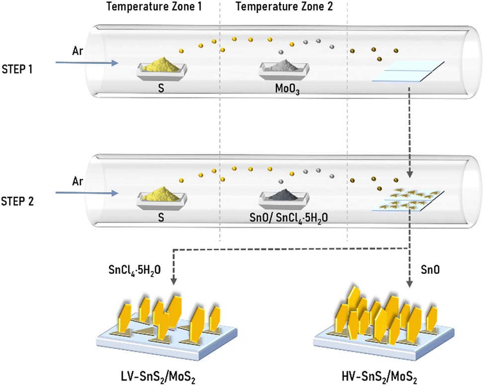 | ||
| Fig. 1 Schematic of two-step direct vdW epitaxial growth of low density-vertical (LV) and high density-vertical (HV) SnS2/MoS2 heterostructures. | ||
Characterization of SnS2/MoS2
The optical micrograph of MoS2 nanosheets on an ITO glass substrate is shown in Fig. 2(a). The randomly deposited island-shaped nanosheets have large areas with diameters of ∼10–20 μm and cover almost 70% of the ITO surface. The sectional-view morphology of the HV-SnS2 sample is characterized by scanning electron microscopy (SEM, Thermo Fisher, Apreo S) in Fig. 2(b). The nanosheets are vertically oriented with a height of ∼500 nm. The SnS2 nanosheets tend to grow out-of-plane on ITO substrate due to the higher surface energy of vertical (100) planes in SnS2.34 Similarly, it is found that SnS2 nanosheets also vertically grow on the ITO with MoS2 nanosheets, which can be observed from SEM images in Fig. 2(c) and (d). Fig. 2(c) and (d) show the top SEM images of LV-SnS2/MoS2 and HV-SnS2/MoS2 heterostructure samples, respectively. These SnS2 nanosheets are well-aligned on MoS2 nanosheets with an edge length of ∼500 nm. Compared with the LV-SnS2/MoS2 heterostructure, the HV-SnS2/MoS2 sample has a higher density, which provides a much larger exposed surface area of HV-SnS2 and a better contact interface between HV-SnS2 and MoS2 nanosheets.26 This heterostructure could accelerate the interfacial charge transportation, which is beneficial for the design of high-performance PEC devices.35,36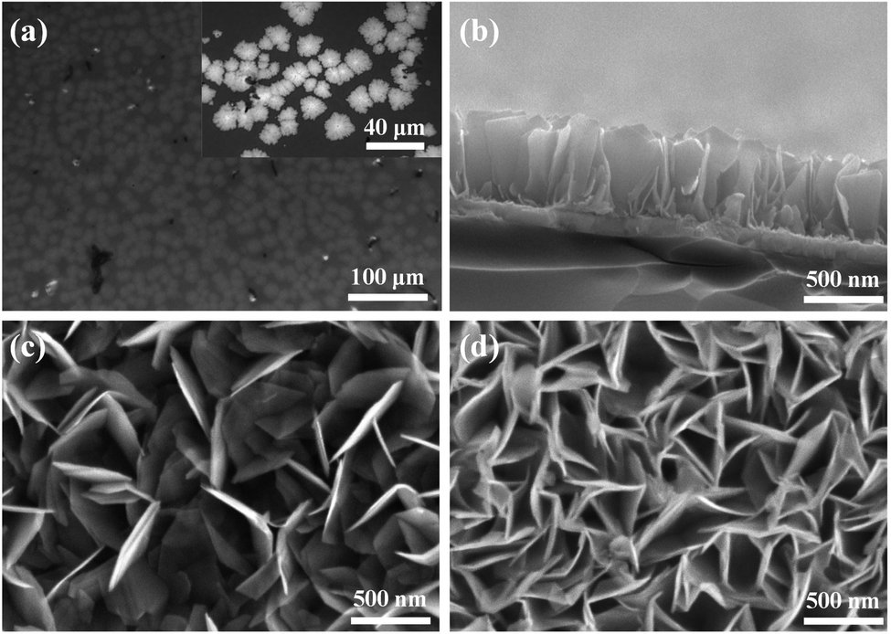 | ||
| Fig. 2 (a) Top optical image of the MoS2 nanosheets. The inset is a high magnification optical image. (b) Sectional-view SEM image of HV-SnS2. (c) Top SEM image of LV-SnS2/MoS2. (d) Top SEM image of HV-SnS2/MoS2. | ||
X-ray diffraction (XRD, Bruker, D8 Advance) is used to analyze the crystallographic structure of the samples, as shown in Fig. 3(a). The main diffraction peaks of HV-SnS2/MoS2 located at 15.05, 28.29, 30.39, 32.09, 41.79, and 46.23° could be attributed to the (001), (100), (002), (011), (012), and (003) crystal planes from 2H-SnS2 (JCPDS 89-2358), respectively. The peak at 35.9° comes from the (102) crystal plane of 2H-MoS2 (JCPDS 37-1492). In the LV-SnS2/MoS2 heterostructure, the (001) and (002) crystal planes of SnS2 and the (102) crystal plane of MoS2 can be observed. The XRD results demonstrate the coexistence and the good crystallinity of SnS2 and MoS2 in the heterostructures.
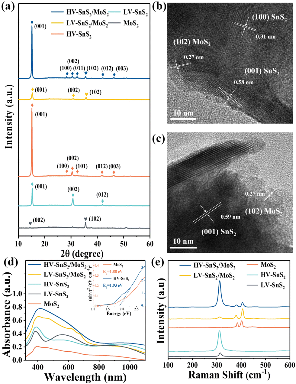 | ||
| Fig. 3 (a) XRD pattern of HV-SnS2/MoS2, LV-SnS2/MoS2, HV-SnS2, LV-SnS2, and MoS2. (b) TEM image of HV-SnS2/MoS2. (c) TEM image of LV-SnS2/MoS2. (d) UV-Vis absorption spectroscopy of all samples. The inset is Tauc plot for estimating the bandgap energies (Eg) of MoS2 and HV-SnS2. (e) Raman spectra of all samples. | ||
To further investigate the crystallinity and internal structure of the vdW heterostructure, a transmission electron microscope (TEM, FEI Tecnai G2 F20) is measured in Fig. 3(b) and (c). The lattice fringes of 0.58 and 0.31 nm can be assigned to the (001) and (100) planes of SnS2, respectively. The lattice fringe of 0.27 nm corresponds to the (102) plane of MoS2. In comparison to the TEM image of HV-SnS2/MoS2, only the (001) plane of SnS2 can be observed in LV-SnS2/MoS2. This result suggests that HV-SnS2/MoS2 might form high density-vertical nanosheets more easily than LV-SnS2/MoS2. The TEM characterization reveals the successful formation of the SnS2/MoS2 heterostructure.
The linear absorption properties of all samples are analyzed by UV-Vis absorption spectroscopy (R1, Ideaoptics) in Fig. 3(d). The result shows that MoS2 nanosheets exhibit a broadband absorption from UV to near-infrared light regions, while HV-SnS2 samples show strong absorption in the UV-Vis region. The superior absorption property of HV-SnS2 nanosheet arrays is related to their excellent light-trapping structure, which could promote internal light scattering and improve the light-harvesting ability.25 For the LV-SnS2/MoS2 sample, the absorption is greatly enhanced in the UV-Vis region due to the construction of the heterostructure. Moreover, the increased nanosheet array density induced an even more significant absorption of HV-SnS2/MoS2. The Eg values of MoS2 and HV-SnS2 are 1.88 and 1.93 eV, respectively, obtained from the Tauc plots as shown in the illustration of Fig. 3(d).
Raman spectra of HV-SnS2, LV-SnS2, MoS2, and heterostructure samples are measured by using the SmartRaman confocal-micro-Raman module (developed by the Institute of Semiconductors, Chinese Academy of Sciences). As shown in Fig. 3(e), the characteristic resonance peak at 311.1 cm−1 corresponds to the A1g mode of SnS2,37 and the characteristic resonance peaks at 383.9 cm−1 and 402.6 cm−1 agree well with the in-plane E2g mode and the out-of-plane A1g mode vibrational modes of MoS2, respectively.31,38 For both HV-SnS2/MoS2 and LV-SnS2/MoS2 heterostructures, the E2g and A1g peaks of MoS2 and the A1g peaks of SnS2 can be identified. These Raman results demonstrate that the HV-SnS2, LV-SnS2, MoS2, and heterostructure samples are successfully prepared.
X-Ray photoelectron spectroscopy (XPS, Thermo Fisher, ESCALAB Xi+) is applied to analyze the bonding configuration, chemical composition, and electronic structure of the samples. The XPS full spectrum of HV-SnS2/MoS2 heterostructure reveals that Sn, Mo, S, O, and C elements coexist in the sample with a very low content of impurities. Fig. 4(a) shows the binding energy peaks of Sn 3d at ∼495.47 and ∼497 eV, which are attributed to Sn 3d3/2 and Sn 3d5/2, respectively, in accordance with the reported values of Sn4+.39 The Sn 3d5/2 peak positions of the HV-SnS2/MoS2 heterostructure and HV-SnS2 have a slight shift of ∼0.1 eV, owing to the strong interaction at the HV-SnS2/MoS2 interface in the heterostructure. Fig. 4(b) shows the peaks of Mo 3d at 232.57 and 229.37 eV, which originate from Mo 3d3/2 and Mo 3d5/2, respectively.40 It can be noted that the Mo 3d5/2 peak in the HV-SnS2/MoS2 heterostructure is absent, probably because of the shielding of the HV-SnS2 and the heterostructure interaction.
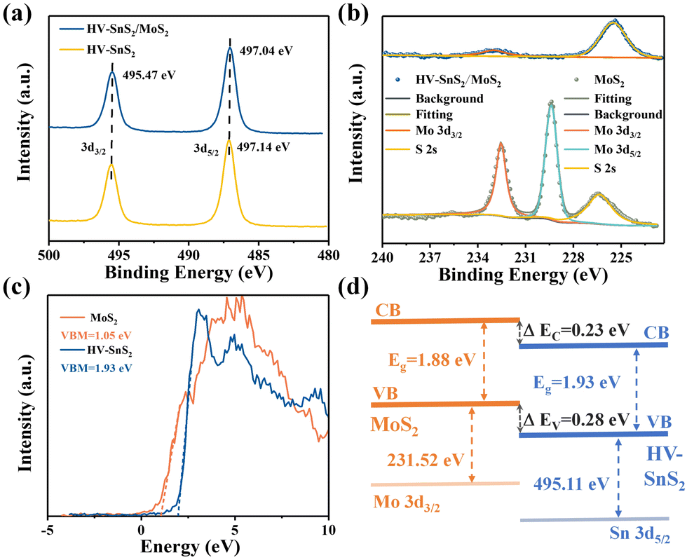 | ||
| Fig. 4 (a) XPS spectra of Sn 3d3/2 and Sn 3d5/2. (b) XPS spectra of Mo 3d3/2 and Mo 3d5/2. (c) VB spectra and VBM fitting of HV-SnS2 and MoS2. (d) Band alignment information of HV-SnS2/MoS2. | ||
To analyze the carrier transportation properties at the heterostructure interface, high-resolution XPS spectra and the valence band maximum (VBM) are measured in Fig. 4(c). Here, the VBM values of HV-SnS2 and MoS2 are obtained to be 1.93 and 1.05 eV, respectively. The type of HV-SnS2/MoS2 heterostructure can be determined by the valence band offset parameter ΔEV and the conduction band offset parameter ΔEC. The ΔEV for the HV-SnS2/MoS2 heterostructure can be calculated via the method from Kraut et al. as41
 | (1) |
The ΔEC can be calculated by
 | (2) |
The band alignment information of HV-SnS2/MoS2 is integrated in Fig. 4(d). The results suggest HV-SnS2/MoS2 forms a type-II heterostructure, which could efficiently promote the interfacial charge separation and improve the performance of optoelectronic devices.42
Photodetector performance of SnS2/MoS2
The photoelectric responses of the samples are measured by a conventional PEC-type system equipped with an electrochemical workstation (CHI660e, Shanghai Chenhua) and a xenon lamp (PLS-SXE300/300UV, Beijing Perfectlight). A platinum (Pt) wire, a mercurous sulfate electrode, and the prepared samples are used as the counter, reference, and working electrodes, respectively. The electrolyte is 1 mol L−1 Na2SO4 neutral solution. The effective illumination area of the photoelectrode is 0.7 cm2.To investigate the light power intensity-dependent photoresponse, the amperometric I–t curves without bias voltage are recorded in Fig. 5(a). By tuning the simulated solar power intensity (P) from level I to level VI (P = 200, 150, 100, 75, 50, 20 mW cm−2), the photocurrent shows a downward trend for all the MoS2, HV-SnS2, LV-SnS2, and heterostructure samples. Meanwhile, the photoresponse of the HV-SnS2/MoS2 heterostructure is far more significant than those of LV-SnS2/MoS2, MoS2, HV-SnS2, and LV-SnS2. More specifically, the values of photocurrent density (Iph) can be extracted by
| Iph = (Ilight − Idark)/S | (3) |
 | ||
| Fig. 5 Photoresponse performances of all samples as photoanodes in 1 M Na2SO4 under 0 V. (a) The amperometric I–t curves irradiated by different simulated solar light power intensities (From I to VI: 200, 150, 100, 75, 50, 20 mW cm−2). (b) Photocurrent density (Iph) and photoresponsivity (Rph) as a function of the light power intensity. (c) The time constants of HV-SnS2/MoS2 for the response (tres) and recovery (trec). (d) The tres and trec of the samples. | ||
Here, we highlight that the excellent photoresponse of the heterostructure samples is obtained without a bias voltage. This advantage implies a potential self-powered photodetector application. Therefore, the photoresponsivity parameter (Rph) is introduced to quantitatively evaluate the self-powered photodetection performance, as defined by
| Rph = Iph/P | (4) |
The Rph values as a function of P are shown in Fig. 5(b) on the right axis. Under the simulated solar light of 200 mW cm−2, the Rph value of the HV-SnS2/MoS2 heterostructure reaches 4.66 mA W−1, which is 2.6, 39.8, 155.3, and 582.5 times higher than those of LV-SnS2/MoS2, MoS2, HV-SnS2, and LV-SnS2, respectively. Even with a weak light of ∼20 mW cm−2, the Rph of the HV-SnS2/MoS2 heterostructure still retains a high value of ∼2.85 mA W−1. For comparison, the previously reported Rph values of many 2D and heterostructure materials are summarized in Table 1. These results reveal that the HV-SnS2/MoS2 heterostructure sample has a superior Rph, which is 1000, 28, 71, 2, and 300 times larger than those of BP,2 PbO,43 Te@Bi,44 and BP/MoS2.45
| Materials | Measurement conditions | I ph (μA cm−2) | R ph (mA W−1) | τ res (ms) | τ rec (ms) | Ref. |
|---|---|---|---|---|---|---|
| HV-SnS2/MoS2 | 1 M Na2SO4, 0 V | 932.8 | 4.7 | 3.6 | 6.4 | This work |
| LV-SnS2/MoS2 | 1 M Na2SO4, 0 V | 357.4 | 1.8 | 3.8 | 8.5 | This work |
| MoS2 | 1 M Na2SO4, 0 V | 33.4 | 0.1 | 5 | 16.3 | This work |
| HV-SnS2 | 1 M Na2SO4, 0 V | 9.3 | 0.03 | 4.1 | 32.8 | This work |
| LV-SnS2 | 1 M Na2SO4, 0 V | 2.47 | 0.008 | 4.2 | 300 | This work |
| BP | 0.1 M Na2SO4, 0 V | 0.26 | 0.002 | 500 | 500 | 2 |
| PbO | 0.01 M KOH, 0 V | 9.8 | 0.1 | — | — | 43 |
| Te@Bi | 0.5 M KOH, 0 V | 4.7 | 0.03 | 80 | 80 | 44 |
| SnS2/TiO2 | 0.5 M Na2SO4, 0 V | 10 | — | — | — | 46 |
| BP/MoS2 | 1 M KOH, 0 V | 2.68 | 0.02 | 51 | — | 45 |
| InSe/Ge-doped InSe | 1 M KOH, 0 V | 0.41 | 0.003 | 95 | 91 | 47 |
| V-SnS2/gra phene | 0.5 M Na2SO4, 0 V | 130 | — | — | — | 48 |
| V-SnS2 | 0.5 M Na2SO4, 1.4 V | 1730 | — | — | — | 34 |
| SnS | 0.1 M Na2SO4, 0.6 V | 1.59 | 0.06 | 300 | — | 49 |
| SnS2/Bi2Se3 | 0.2 M Na2SO3, −0.1 V | 170 | 2.43 | — | — | 30 |
| TiO2/SnS2/CoOx | 0.5 M Na2SO4, 0.65 V | 1050 | — | — | — | 50 |
| V-SnS2 | FET, 490 nm Vds = 2 V | 0.043 | — | 43.4 | 64.4 | 51 |
| SnS2/MoS2 | FET, visible Vds = 1 V | 4 × 10⁵ | 2.3 | 100 | — | 52 |
| SnS2/perovskite | FET, 445 nm Vds = −3 V | 1050 | — | 0.02 | 0.03 | 53 |
In addition to Rph, the response time (tres) and recovery time (trec) are essential parameters for assessing the response speed of photodetectors. The tres and trec could be assigned to the time interval of photocurrent density change from 10% to 90% and from 90% to 10% of its peak value, respectively.43 From Fig. 5(c), the HV-SnS2/MoS2 sample exhibits a remarkably fast response with tres = 3.6 ms and trec = 6.4 ms as the self-powered PEC photodetector. Additionally, the summarized time constants of HV-SnS2, LV-SnS2, MoS2, and heterostructure samples are shown in Fig. 5(d), and the previously reported results of other 2D materials are listed in Table 1. These results suggest HV-SnS2/MoS2 has a superior response speed compared with BP2, Te@Bi,44 SnS,49 BP/MoS2,45 SnS2 (FET),54 and SnS2/MoS2 (FET)52 based photodetectors. Meanwhile, compared with voltage-driven photodetectors based on MoS2 and SnS2 heterostructures,34,48,50–53,55,56 the HV-SnS2/MoS2 self-powered photodetector shows a fast response time but relatively lower photocurrent density and responsivity. To improve the photodetection capability of HV-SnS2/MoS2, applying an external bias may be an efficient way to accelerate the charge transport process.
To further explore the sensitivity this self-powered photodetector, the wavelength-dependent response is measured. Fig. 6(a) shows the wavelength dependence of the photocurrent density under quasi-monochromatic light irradiation at 350, 380, 420, 450, 475, 500, 520, 550, 600, and 650 nm. The light power intensity maintains a constant of 10 mW cm−2. Moreover, the Iph values are extracted as shown in Fig. 6(b) to give a clear comparison. All these samples show the highest Iph at 420 nm, according well with the absorption spectra in UV-Vis results (Fig. 3(a)). The HV-SnS2/MoS2 heterostructure exhibits the largest Iph under all the measured wavelengths, and the maximum Iph of HV-SnS2/MoS2 at 420 nm reaches ∼118.25 μA cm−2, which is 1.9, 9.1, 11.5, and 11.6 times larger than those of LV-SnS2/MoS2, MoS2, HV-SnS2, and LV-SnS2, respectively. The result originates from the special morphology improving light absorption and type-II heterostructure accelerating separation of electron–hole pairs. To make a more general comparison, the Rph values that do not contain the power intensity are calculated and shown in Fig. 6(b) on the right axis. The changing of Rph is proportional to Iph because the P is a constant 10 mW cm−2 in the measurement. The HV-SnS2/MoS2 sample also exhibits the highest sensitivity at 420 nm with the maximum Rph of 11.82 mA W−1, which is much more significant than the reported 0.76, 0.54, 0.37, and 0.41 of graphdiyne (∼400 nm),57 Bi2Te3 (∼400 nm),58 Bi/Te (∼400 nm),59 and ZnO/NiO (∼350 nm),60 respectively. These results suggest that the HV-SnS2/MoS2-based photodetector can be used in the UV-Vis region.
 | ||
| Fig. 6 (a) The amperometric I–t curves irradiated by light at different wavelengths. (b) Iph and Rph as a function of wavelength. (c) The amperometric I–t curves irradiated by light in 400+ and 420+ nm. (d) The amperometric I–t curves irradiated by light in 700+ and 800+ nm. | ||
In the following part, we verify the self-powered photoresponse properties of HV-SnS2/MoS2 for visible and infrared detection applications. Different wavelength bands of 400+, 420+, 700+, and 800+ nm are achieved by using cut-off filters. Fig. 6(c) shows the visible light detection performances of the samples under 400+ and 420+ nm irradiation. The HV-SnS2/MoS2 heterostructure offers the best performance, with the photocurrent density reaching 205.9 μA cm−2 under 400+ nm irradiation, which is 4.7, 10.3, 13.4, and 36.4 times larger than those of LV-SnS2/MoS2, MoS2, HV-SnS2, and LV-SnS2, respectively. It is worth mentioning that the HV-SnS2/MoS2 heterostructure can also be used as an infrared photodetector. As proved in Fig. 6(d), relatively high photocurrent densities of approximately 2.63 and 0.92 μA cm−2 are achieved by HV-SnS2/MoS2 heterostructure under 700+ and 800+ nm irradiation, respectively. The below bandgap absorption may be from the intrinsic defects, such as S vacancies13 and the surface oxidation.61
To understand the charge and mass transfer processes at the photoelectrode/electrolyte interface, electrochemical impedance spectra (EIS) were measured from 10−2 to 105 Hz, as shown in Fig. 7(a). The inset shows the equivalent circuit consisting of Rs, Rct, and CPE, which represent the electrolyte solution resistance, the charge transfer resistance, and the interfacial capacitance, respectively. The HV-SnS2/MoS2 heterostructure possesses the smallest semicircle radius, suggesting the lowest charge transfer impedance and the highest charge transfer efficiency at the interface between the photoelectrode and the electrolyte. Additionally, the EIS Bode phase plots (Fig. 7(b)) also can reveal the interfacial mass and charge transfer in the low and middle-frequency range (10−2 to 103 Hz). The frequency (fmax) corresponding to the characteristic peak shifts toward lower frequency region after the construction of type-II HV-SnS2/MoS2 heterostructure, suggesting a high-efficiency channel for charge transfer and ion diffusion at the interface between the photoelectrode and the electrolyte.62
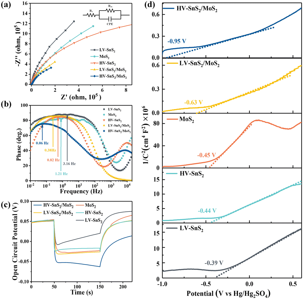 | ||
| Fig. 7 (a) EIS-Nyquist plots of all samples. The illustration is an equivalent circuit model. (b) EIS-Bode phase plots of all samples. (c) Open circuit potential of all samples. (d) Mott–Schottky curves of all samples. | ||
In order to characterize the generation, accumulation, and recombination of electron–hole pairs,25 the open-circuit potential (Voc) is carried out by monitoring the photoelectrode from a light irradiated quasi-equilibrium state to a dark state. Under light illumination, the photoexcited electrons transfer and accumulate into the conduction band (CB) of the material, leading to a downswing of the Fermi level to a more negative potential.63 Under the dark state, the Voc decays rapidly because the accumulated electrons will be consumed by holes.64 As shown in Fig. 7(c), the HV-SnS2/MoS2 has a potential of −0.05 V, which is more negative than those of LV-SnS2/MoS2 (−0.029 V), MoS2 (−0.026 V), HV-SnS2 (−0.017 V), and LV-SnS2 (−0.007 V). These results suggest that the accumulation of photoexcited electrons in the CB from MoS2 to HV-SnS2 could be accelerated by the interfacial separation of electron–hole pairs in the heterostructure.
Mott–Schottky plots of the photoelectrodes are measured in Fig. 7(d). All the samples are n-type semiconductors inferred from the positive slope of the curves.65 The charge carrier density (ND) of semiconductors can be calculated using the formula66
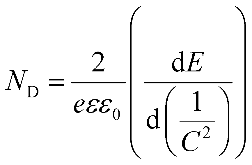 | (5) |
 | (6) |
Furthermore, we have also investigated the PEC photodetection performances of these samples under non-zero voltages. Previous studies have revealed that the bias voltage is an efficient way to accelerate the charge transport process. The photoresponses of the HV-SnS2/MoS2 sample under different bias voltages are shown in Fig. 8(a). To evaluate the performance of the photodetector, the Iph and Rph values are extracted as shown in Fig. 8(b). Under 0.8 V, the Iph of HV-SnS2/MoS2 reaches a maximum of 213 μA cm−2, which is 25, 1.9, 1.6, and 1.2 times higher than those values measured at −0.2, 0, 0.4, and 0.9 V. Similarly, the values of Rph are proportional to Iph due to the same measured Pλ (100 mW cm−2). The external applied positive voltage could establish a potential gradient within the samples, thus accelerating the charge transport and carrier separation68 and leading to a better PEC performance. Under the optimal condition of 0.8 V, the photoresponses of HV-SnS2/MoS2, LV-SnS2/MoS2, MoS2, HV-SnS2, and LV-SnS2 are measured in Fig. 8(c), and the calculated Iph and Rph values are shown in Fig. 8(d). This result suggests that the HV-SnS2/MoS2 heterostructure offers more active sites and efficient charge transportation, benefitting PEC water splitting.
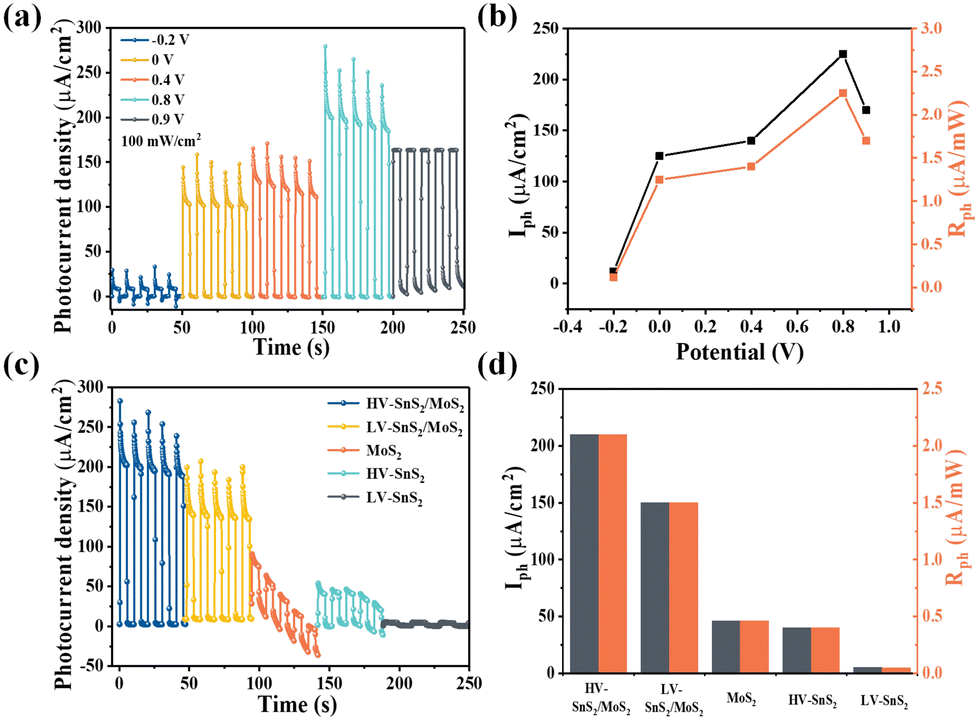 | ||
| Fig. 8 (a) The amperometric I–t curves of HV-SnS2/MoS2 under different bias voltages. (b) Iph and Rph of HV-SnS2/MoS2 as a function of bias voltage. (c) The amperometric I–t curves of different photoelectrodes under 0.8 V. (d) Iph and Rph of different photoelectrodes under 0.8 V. | ||
Photoelectrocatalytic hydrogen production
The current loop in PEC photodetectors is connected by exchanging electrons with the electrolyte, which may produce hydrogen (H2) and oxygen (O2) evolution at the electrode/electrolyte interface. In order to investigate the PEC water splitting mechanism and photoelectric process, we investigate the PEC water splitting and photoelectrocatalytic H2 evolution of the multifunctional HV-SnS2/MoS2-based PEC photodetector. The photoelectrocatalytic H2 production measurements of these samples are performed in a quartz glass reaction cell equipped with a gas analysis vacuum system (Labsolar-6A, Beijing Perfectlight). The reaction unit is a conventional three-electrode system under a 100 mW cm−2 simulated solar light irradiation (300 W, PLS-SXE300, Beijing Perfectlight). The electrolyte is 100 mL 1 M Na2SO4 aqueous solution without adding any sacrificial reagent. The amount of the generated H2 is analyzed using a gas chromatograph (GC9790II, Fuli instrument).Fig. 9(a) shows the H2 evolution of the samples and the ITO reference gated at 0.8 V. The ITO has no evident H2 production, indicating that the measured H2 contributes to the electrode. The produced H2 from the HV-SnS2/MoS2 heterostructure reaches 6.8 μmol cm−2 within 2.5 h, which is 1.4, 3.4, 3.6, and 5.6 times higher than those from LV-SnS2/MoS2 (4.9 μmol cm−2), MoS2 (2.0 μmol cm−2), HV-SnS2 (1.9 μmol cm−2), and LV-SnS2 (1.2 μmol cm−2). This improvement of H2 production in the HV-SnS2/MoS2 heterostructure might be due to the efficient electron charge transportation at the interface between HV-SnS2 and MoS2 and the low recombination rate of electron–hole pairs. Conversely, the weak photoelectrocatalytic for H2 production of pure LV-SnS2, HV-SnS2, and MoS2 is mainly because of the high recombination rate of the electron–hole pairs.69 However, the H2 production rate is higher in the first cycle than in the latter, which could be induced by the degraded photo-activity70 and/or the gradual degradation71 of the photoanode.
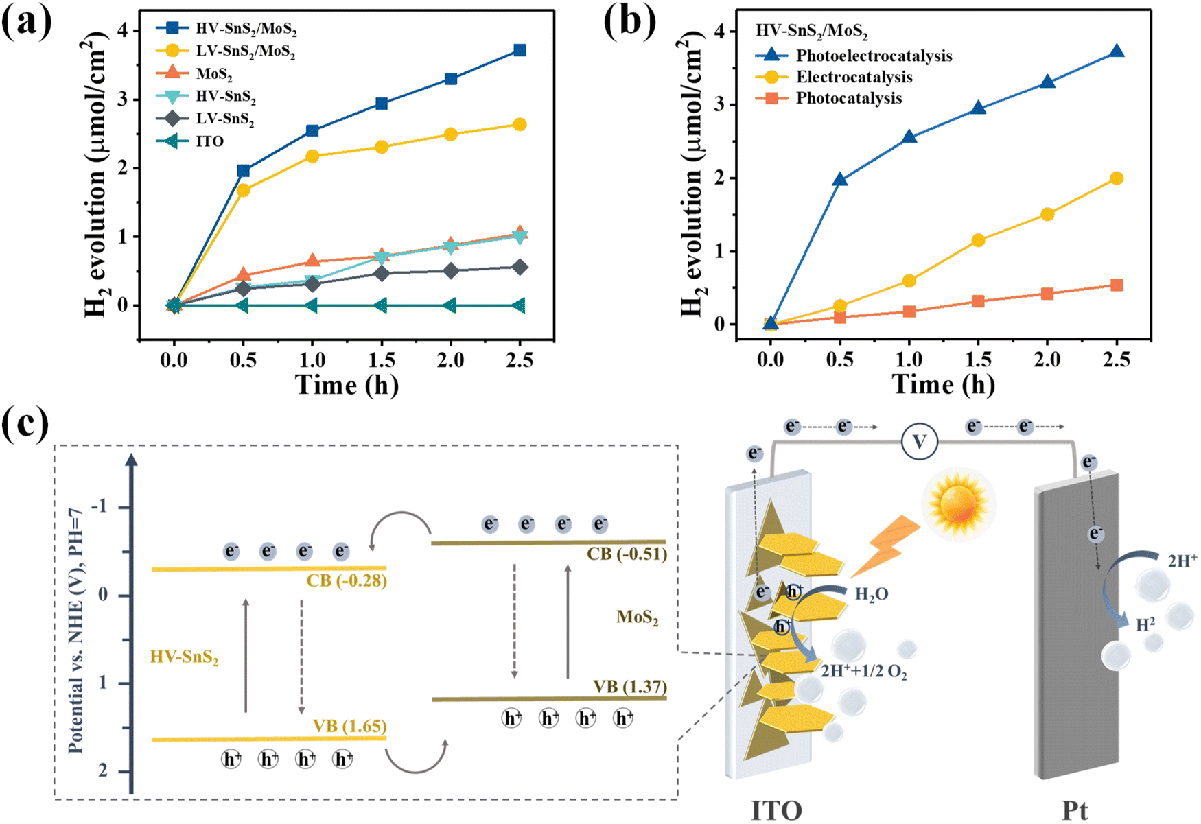 | ||
| Fig. 9 (a) Photoelectrocatalytic H2 production of different photoanodes in 1 M Na2SO4 under 0.8 V. (b) Photocatalytic (100 mW cm−2), electrocatalytic (0.8 V), and photoelectrocatalytic (100 mW cm−2, 0.8 V) H2 production of HV-SnS2/MoS2 photoanode. (c) The schematic plot of charge transfer pathways in HV-SnS2/MoS2 heterostructure as an effective photoelectrode for PEC water splitting. | ||
To further explore the contribution of photocatalysis and electrocatalysis, the H2 production of the HV-SnS2/MoS2 heterostructure under 0.8 V without light illumination (electrocatalysis) and under 100 mW cm−2 without applied bias potential (photocatalysis) are measured and shown in Fig. 9(b). The electrocatalytic H2 production within 2.5 h is 3.74 μmol cm−2, which is superior to 1.18 μmol cm−2 from photocatalytic H2 production. The mechanism of electrocatalytic H2 production can be attributed to the higher applied bias voltage (0.997 VNHE, calculated by ENHE = E(Ag/AgCl) + 0.197) than the potential of the cathodic (Pt) H2 evolution reaction.72 The effect of photocatalytic H2 production is mainly due to the enhanced separation of the photoexcited charge and the more negative CB potential of samples than the H+/H2 potential (0 VNHE).73 Notably, the photoelectrocatalytic H2 production of HV-SnS2/MoS2 is 6.79 μmol cm−2, which is larger than the total H2 production of photocatalysis and electrocatalysis processes. This result suggests that the synergistic effect of input light activation and applied voltage may accelerate the charge separation and transportation processes.74
Based on the above-mentioned results and discussion, the PEC water splitting mechanism of the HV-SnS2/MoS2 heterostructure is investigated in Fig. 9(c). Because the CB potential is approximately 0.3 V lower than the VFB of the n-type semiconductor,75 the corresponding CB potential of MoS2 and HV-SnS2 are calculated as −0.51 and −0.28 V vs. NHE (vs. the H+/H2 potential of 0.0 VNHE76,77), respectively. According to the band alignment of HV-SnS2/MoS2, the energy level arrangement and charge transfer pathways of HV-SnS2/MoS2 are depicted in Fig. 9(c). With simulated light irradiation, the photoexcited electrons are excited from VB to CB in both MoS2 and HV-SnS2. At the interface of the HV-SnS2/MoS2 heterostructure, the electrons transfer from MoS2 to HV-SnS2 in the CB, then flow to the Pt electrode, and reduce H+ ions to form H2 (2h+ + 2e− → H2). In this process, the charge transfer could be accelerated by the bias voltages, thus boosting the electron transfer to the Pt electrode and improving the H2 production. In contrast, the hole-transfer pathway is from HV-SnS2 to MoS2 in the VB. Then, the holes move to the photoelectrode/electrolyte interface and oxidize OH− ions for producing O2 (2H2O + 2h+ → O2 + 4e− + 4H+). Therefore, the reverse transmission direction of electrons and holes in HV-SnS2/MoS2 will efficiently separate electron–hole pairs and decrease their recombination at the heterostructure interface, thus leading to higher H2 production.
Conclusions
SnS2/MoS2 heterostructures with trap-like vertically oriented nanostructures were synthesized through a two-step CVD method. The synthesized HV-SnS2/MoS2-based PEC photodetector demonstrates excellent self-powered performances, including significantly enhanced photocurrent densities, sensitivity, and stability than those of HV-SnS2, LV-SnS2, MoS2, and LV-SnS2/MoS2 heterostructures. The UV-Vis, EIS, V–t, and Mott–Schottky results show that the HV-SnS2/MoS2 heterostructure has the optimal light absorption range and capacity, the smallest electron transfer impedance, and the highest carrier density. The greatly improved PEC performance of heterostructures could be ascribed to two reasons: (i) the outstanding type-II band alignment at the SnS2/MoS2 interface of the heterostructure, which can accelerate the separation and transport of photoexcited charge carriers; (ii) the abundant active sites of high-density vertical SnS2 on MoS2 nanosheets, which contribute to more enhanced light absorption. The results could enrich exploration ideas for 2D material-based optoelectronic and PEC applications for photodetection, solar cell, water splitting, and photocatalysis.Conflicts of interest
There are no conflicts to declare.Acknowledgements
This work was supported by the National Natural Science Foundation of China (No. 11974279 and 12074311).References
- J. Zhou, L. Chen, Y. Wang, Y. He, X. Pan and E. Xie, Nanoscale, 2016, 8, 50–73 RSC.
- X. Ren, Z. Li, Z. Huang, D. Sang, H. Qiao, X. Qi, J. Li, J. Zhong and H. Zhang, Adv. Funct. Mater., 2017, 27, 1606834 CrossRef.
- X. Ren, W. Zheng, H. Qiao, L. Ren, S. Liu, Z. Huang, X. Qi, Z. Wang, J. Zhong and H. Zhang, Mater. Today Energy, 2020, 16, 100401 CrossRef.
- H. Qiao, Z. Huang, X. Ren, S. Liu, Y. Zhang, X. Qi and H. Zhang, Adv. Opt. Mater., 2019, 8, 1900765 CrossRef.
- L. Peng, L. F. Hu and X. S. Fang, Adv. Funct. Mater., 2014, 24, 2591–2610 CrossRef CAS.
- S. M. Hatch, J. Briscoe and S. Dunn, Adv. Mater., 2013, 25, 867–871 CrossRef CAS PubMed.
- Y. Yang, W. Guo, J. Qi, J. Zhao and Y. Zhang, Appl. Phys. Lett., 2010, 97, 223113 CrossRef.
- Y. Xie, L. Wei, G. Wei, Q. Li, D. Wang, Y. Chen, S. Yan, G. Liu, L. Mei and J. Jiao, Nanoscale Res. Lett., 2013, 8, 188 CrossRef PubMed.
- C. Jin, E. Y. Ma, O. Karni, E. C. Regan, F. Wang and T. F. Heinz, Nat. Nanotechnol., 2018, 13, 994–1003 CrossRef CAS PubMed.
- J. Zhang, S. Chen, Y. Ma, D. Wang, J. Zhang, Y. Wang, W. Li, Z. Yu, H. Zhang, F. Yin and Z. Li, J. Mater. Chem. B, 2018, 6, 4065–4070 RSC.
- B. Radisavljevic, A. Radenovic, J. Brivio, V. Giacometti and A. Kis, Nat. Nanotechnol., 2011, 6, 147–150 CrossRef CAS PubMed.
- C. Choi, M. K. Choi, S. Liu, M. S. Kim, O. K. Park, C. Im, J. Kim, X. Qin, G. J. Lee, K. W. Cho, M. Kim, E. Joh, J. Lee, D. Son, S.-H. Kwon, N. L. Jeon, Y. M. Song, N. Lu and D.-H. Kim, Nat. Commun., 2017, 8, 1664 CrossRef PubMed.
- Y. Xie, B. Zhang, S. Wang, D. Wang, A. Wang, Z. Wang, H. Yu, H. Zhang, Y. Chen, M. Zhao, B. Huang, L. Mei and J. Wang, Adv. Mater., 2017, 29, 1605972 CrossRef PubMed.
- S. M. Bahauddin, H. Robatjazi and I. Thomann, ACS Photonics, 2016, 3, 853–862 CrossRef CAS.
- P. Gant, P. Huang, D. Pérez de Lara, D. Guo, R. Frisenda and A. Castellanos-Gomez, Mater. Today, 2019, 27, 8–13 CrossRef CAS.
- R. Yalavarthi, A. Naldoni, Š. Kment, L. Mascaretti, H. Kmentová, O. Tomanec, P. Schmuki and R. Zbořil, Catalysts, 2019, 9, 204 CrossRef.
- I. S. Cho, C. H. Lee, Y. Feng, M. Logar, P. M. Rao, L. Cai, D. R. Kim, R. Sinclair and X. Zheng, Nat. Commun., 2013, 4, 1723 CrossRef PubMed.
- K. Jarasiunas, L. Bastiene, J. C. Launay, P. Delaye and G. Roosen, Semicond. Sci. Technol., 1999, 14, 48–57 CrossRef CAS.
- J. Shi, H. n Cui, Z. Liang, X. Lu, Y. Tong, C. Su and H. Liu, Energy Environ. Sci., 2011, 4, 466–470 RSC.
- Y. Zhang, W. Xu, X. Xu, W. Yang, S. Li, J. Chen and X. Fang, Nanoscale Horiz., 2019, 4, 452–456 RSC.
- E. Lopriore, E. G. Marin and G. Fiori, Nanoscale Horiz., 2022, 7, 41–50 RSC.
- Y. Xiao, C. Feng, J. Fu, F. Wang, C. Li, V. F. Kunzelmann, C.-M. Jiang, M. Nakabayashi, N. Shibata, I. D. Sharp, K. Domen and Y. Li, Nat. Catal., 2020, 3, 932–940 CrossRef CAS.
- P. Guo, J. Jiang, S. Shen and L. Guo, Int. J. Hydrogen Energy, 2013, 38, 13097–13103 CrossRef CAS.
- B. Thangaraju and P. Kaliannan, J. Phys. D: Appl. Phys., 2000, 33, 1054–1059 CrossRef CAS.
- J. Mu, H. Miao, E. Liu, J. Feng, F. Teng, D. Zhang, Y. Kou, Y. Jin, J. Fan and X. Hu, Nanoscale, 2018, 10, 11881–11893 RSC.
- H. Zhong, G. Yang, H. Song, Q. Liao, H. Cui, P. Shen and C.-X. Wang, J. Phys. Chem. C, 2012, 116, 9319–9326 CrossRef CAS.
- B. Giri, M. Masroor, T. Yan, K. Kushnir, A. D. Carl, C. Doiron, H. Zhang, Y. Zhao, A. Mcclelland and G. A. J. A. E. M. Tompsett, Adv. Energy Mater., 2019, 9, 1901236 CrossRef.
- G. Su, V. G. Hadjiev, P. E. Loya, J. Zhang, S. Lei, S. Maharjan, P. Dong, P. M. Ajayan, J. Lou and H. Peng, Nano Lett., 2015, 15, 506–513 CrossRef CAS PubMed.
- B. Li, L. Huang, M. Z. Zhong, Y. Li, Y. Wang, J. B. Li and Z. M. Wei, Adv. Electron. Mater., 2016, 2, 1600298 CrossRef.
- M. Luo, C. Lu, Y. Liu, T. Han, Y. Ge, Y. Zhou and X. Xu, Sci. China Mater., 2022, 65, 1000–1011 CrossRef CAS.
- K. Chen, X. Wan, J. Wen, W. Xie, Z. Kang, X. Zeng, H. Chen and J.-B. Xu, ACS Nano, 2015, 9, 9868–9876 CrossRef CAS PubMed.
- Y. Zhang, Y. Liu, R. Li, M. Saddam Khan, P. Gao, Y. Zhang and Q. Wei, Sci. Rep., 2017, 7, 4629 CrossRef PubMed.
- D. B. Seo, T. N. Trung, S. S. Bae and E. T. Kim, Nanomaterials, 2021, 11, 1585 CrossRef CAS PubMed.
- G. Liu, Z. Li, T. Hasan, X. Chen, W. Zheng, W. Feng, D. Jia, Y. Zhou and P. Hu, J. Mater. Chem. A, 2017, 5, 1989–1995 RSC.
- X. Tan, X. Wang, L. Zhang, L. Liu, G. Zheng, H. Li and F. Zhou, Anal. Chem., 2019, 91, 8274–8279 CrossRef CAS PubMed.
- L. Chen, E. Liu, F. Teng, T. Zhang, J. Feng, Y. Kou, Q. Sun, J. Fan, X. Hu and H. Miao, Appl. Surf. Sci., 2019, 467-468, 698–707 CrossRef CAS.
- Q. Yang, K. B. Tang, C. R. Wang, D. Y. Zhang and Y. T. Qian, J. Solid State Chem., 2002, 164, 106–109 CrossRef CAS.
- H. Li, Q. Zhang, C. C. R. Yap, B. K. Tay, T. H. T. Edwin, A. Olivier and D. Baillargeat, Adv. Funct. Mater., 2012, 22, 1385–1390 CrossRef CAS.
- C. Z. Yong, N. D. Zhen, K. W. Li, Z. J. S. Ming and P. Technology, Sep. Purif. Technol., 2011, 81, 101–107 CrossRef.
- C. H. Lu, J. Y. Ma, K. Y. Si, X. Xu, C. J. Quan, C. He and X. L. Xu, Phys. Status Solidi A, 2019, 216, 1900544 CrossRef CAS.
- E. A. Kraut, R. W. Grant, J. R. Waldrop and S. P. J. P. R. L. Kowalczyk, Phys. Rev. Lett., 1980, 44, 1620–1623 CrossRef CAS.
- S. Han, Y.-C. Pu, L. Zheng, J. Z. Zhang and X. Fang, J. Mater. Chem. A, 2015, 3, 22627–22635 RSC.
- C. Xing, X. Chen, W. Huang, Y. Song, J. Li, S. Chen, Y. Zhou, B. Dong, D. Fan, X. Zhu and H. Zhang, ACS Photonics, 2018, 5, 5055–5067 CrossRef CAS.
- Y. Zhang, F. Zhang, L. Wu, Y. Zhang, W. Huang, Y. Tang, L. Hu, P. Huang, X. Zhang and H. Zhang, Small, 2019, 15, e1903233 CrossRef PubMed.
- H. Qiao, Z. Li, Z. Huang, X. Ren, J. Kang, M. Qiu, Y. Liu, X. Qi, J. Zhong and H. Zhang, Appl. Mater. Today, 2020, 20, 100765 CrossRef.
- L. Sun, Z. Zhao, S. Li, Y. Su, L. Huang, N. Shao, F. Liu, Y. Bu, H. Zhang and Z. Zhang, ACS Appl. Nano Mater., 2019, 2, 2144–2151 CrossRef CAS.
- L. Liao, B. Wu, E. Kovalska, F. M. Oliveira, J. Azadmanjiri, V. Mazanek, L. Valdman, L. Spejchalova, C. Xu, P. Levinsky, J. Hejtmanek and Z. Sofer, Nanoscale, 2022, 14, 5412–5424 RSC.
- D.-B. Seo, M.-S. Kim, T. N. Trung and E.-T. Kim, Electrochim. Acta, 2020, 364, 137164 CrossRef CAS.
- W. Huang, Z. Xie, T. Fan, J. Li, Y. Wang, L. Wu, D. Ma, Z. Li, Y. Ge, Z. N. Huang, X. Dai, Y. Xiang, J. Li, X. Zhu and H. Zhang, J. Mater. Chem. C, 2018, 6, 9582–9593 RSC.
- Z. Cao, Y. Yin, P. Fu, D. Li, Y. Zhou, Y. Deng, Y. Peng, W. Wang, W. Zhou and D. Tang, Nanoscale Res. Lett., 2019, 14, 342 CrossRef PubMed.
- G. Liu, Z. Li, X. Chen, W. Zheng, W. Feng, M. Dai, D. Jia, Y. Zhou and P. Hu, Nanoscale, 2017, 9, 9167–9174 RSC.
- C. S. R. Kolli, V. Selamneni, B. A. Muñiz Martínez, A. Fest Carreno, D. Emanuel Sanchez, M. Terrones, E. Strupiechonski, A. De Luna Bugallo and P. Sahatiya, ACS Appl. Mater. Interfaces, 2022, 14, 15415–15425 CrossRef CAS PubMed.
- L. Shooshtari, A. Esfandiar, Y. Orooji, M. Samadpour and R. Rahighi, Sci. Rep., 2021, 11, 19353 CrossRef CAS PubMed.
- Q. Fu, H. Mo, K. Ostrikov, X. Gu, H. Nan and S. Xiao, CrystEngComm, 2021, 23, 2563–2571 RSC.
- D.-B. Seo, T. N. Trung, D.-O. Kim, D. V. Duc, S. Hong, Y. Sohn, J.-R. Jeong and E.-T. Kim, Nano-Micro Lett., 2020, 12, 172 CrossRef CAS PubMed.
- L. Shooshtari, S. Ghods, R. Mohammadpour, A. Esfandiar and A. Iraji zad, Sci. Rep., 2022, 12, 7227 CrossRef CAS PubMed.
- Y. Zhang, P. Huang, J. Guo, R. Shi, W. Huang, Z. Shi, L. Wu, F. Zhang, L. Gao, C. Li, X. Zhang, J. Xu and H. Zhang, Adv. Mater., 2020, 32, e2001082 CrossRef PubMed.
- Y. Zhang, Q. You, W. Huang, L. Hu, J. Ju, Y. Ge and H. Zhang, Nanoscale Adv., 2020, 2, 1333–1339 RSC.
- Y. Zhang, J. Guo, Y. Xu, W. Huang, C. Li, L. Gao, L. Wu, Z. Shi, C. Ma, Y. Ge, X. Zhang and H. Zhang, Nanoscale Horiz., 2020, 5, 847–856 RSC.
- C. Wei, J. Xu, S. Shi, R. Cao, J. Chen, H. Dong, X. Zhang, S. Yin and L. Li, J. Mater. Chem. C, 2019, 7, 9369–9379 RSC.
- Y.-R. Chang, P.-H. Ho, C.-Y. Wen, T.-P. Chen, S.-S. Li, J.-Y. Wang, M.-K. Li, C.-A. Tsai, R. Sankar, W.-H. Wang, P.-W. Chiu, F.-C. Chou and C.-W. Chen, ACS Photonics, 2017, 4, 2930–2936 CrossRef CAS.
- C. J. Liu, Y. H. Yang, W. Z. Li, J. Li, Y. M. Li, Q. L. Shi and Q. Y. Chen, ACS Appl. Mater. Interfaces, 2015, 7, 10763–10770 CrossRef CAS PubMed.
- Y. Yin, E. Liu, H. Li, J. Wan, J. Fan, X. Hu, J. Li, C. Tang and C. J. C. I. Pu, Ceram. Int., 2016, 9387–9395 CrossRef CAS.
- H. Yang, C. Guo, G. H. Guai, Q. Song, S. P. Jiang and C. M. Li, ACS Appl. Mater. Interfaces, 2011, 3, 1940–1945 CrossRef CAS PubMed.
- Y. Liu, F. Le Formal, F. Boudoire, L. Yao, K. Sivula and N. Guijarro, J. Mater. Chem. A, 2019, 7, 1669–1677 RSC.
- F. Cao, J. Xiong, F. Wu, Q. Liu, Z. Shi, Y. Yu, X. Wang and L. Li, ACS Appl. Mater. Interfaces, 2016, 8, 12239–12245 CrossRef CAS PubMed.
- Q. Liu, H. Lu, Z. Shi, F. Wu, J. Guo, K. Deng and L. Li, ACS Appl. Mater. Interfaces, 2014, 6, 17200–17207 CrossRef CAS PubMed.
- Z. J. Li, H. Qiao, Z. N. Guo, X. H. Ren, Z. Y. Huang, X. Qi, S. C. Dhanabalan, J. S. Ponraj, D. Zhang, J. Q. Li, J. L. Zhao, J. X. Zhong and H. Zhang, Adv. Funct. Mater., 2018, 28, 1705237 CrossRef.
- J. Xu and X. Cao, Chem. Eng. J., 2015, 260, 642–648 CrossRef CAS.
- J. Kim, W. Yang, Y. Oh, H. Lee, S. Lee, H. Shin, J. Kim and J. Moon, J. Mater. Chem. A, 2017, 5, 2180–2187 RSC.
- F. Jiang, Gunawan, T. Harada, Y. Kuang, T. Minegishi, K. Domen and S. Ikeda, J. Am. Chem. Soc., 2015, 137, 13691–13697 CrossRef CAS PubMed.
- X. Li, X. Hao, A. Abudula and G. Guan, J. Mater. Chem. A, 2016, 4, 11973–12000 RSC.
- X. Wang, X. Wang, J. Huang, S. Li, A. Meng and Z. Li, Nat. Commun., 2021, 12, 4112 CrossRef CAS PubMed.
- J. Zhang, X. Zhang and L. Lei, Sci. Bull., 2008, 53, 1929–1932 CrossRef CAS.
- W. Yin, L. Bai, Y. Zhu, S. Zhong, L. Zhao, Z. Li and S. Bai, ACS Appl. Mater. Interfaces, 2016, 8, 23133–23142 CrossRef CAS PubMed.
- M. Faraji, M. Yousefi, S. Yousefzadeh, M. Zirak, N. Naseri, T. H. Jeon, W. Choi and A. Z. Moshfegh, Energy Environ. Sci., 2019, 12, 59–95 RSC.
- R. Sathre, J. B. Greenblatt, K. Walczak, I. D. Sharp, J. C. Stevens, J. W. Ager and F. A. Houle, Energy Environ. Sci., 2016, 9, 803–819 RSC.
Footnote |
| † Yuqi Liu and Chunhui Lu contributed equally to this work. |
| This journal is © The Royal Society of Chemistry 2022 |