DOI:
10.1039/D1NH00481F
(Communication)
Nanoscale Horiz., 2022,
7, 299-310
Versatile memristor for memory and neuromorphic computing†
Received
14th September 2021
, Accepted 14th January 2022
First published on 14th January 2022
Abstract
The memristor is a promising candidate to implement high-density memory and neuromorphic computing. Based on the characteristic retention time, memristors are classified into volatile and non-volatile types. However, a single memristor generally provides a specific function based on electronic performances, which poses roadblocks for further developing novel circuits. Versatile memristors exhibiting both volatile and non-volatile properties can provide multiple functions covering non-volatile memory and neuromorphic computing. In this work, a versatile memristor with volatile/non-volatile bifunctional properties was developed. Non-volatile functionality with a storage window of 4.0 × 10⁵ was obtained. Meanwhile, the device can provide threshold volatile functionalities with a storage window of 7.0 × 10⁴ and a rectification ratio of 4.0 × 10⁴. The leaky integrate-and-fire (LIF) neuron model and artificial synapse based on the device have been studied. Such a versatile memristor enables non-volatile memory, selectors, artificial neurons, and artificial synapses, which will provide advantages regarding circuit simplification, fabrication processes, and manufacturing costs.
New concepts
There is an important demand for novel memristive devices enabling non-volatile memory and neuromorphic computing. Particularly, the device emulates both short- and long-term synaptic plasticity, as well as neuron-like threshold switching. This novel memristor would simplify circuit design, lower energy consumption, and increase the scalability of memory and computation hardware, paving the way for edge computing applications. In this work, a versatile memristor covering the multiple roles of non-volatile memory, selectors, artificial neurons, and artificial synapses was developed for the first time. Ag atom dynamics in the CuInSe2 (CIS) have been investigated to reveal appealing properties. The results benefit the development of memristive physics, advanced data storage, and neuromorphic computing systems.
|
1. Introduction
Modern computers need higher-density memory and more effective computation for integration into numerous areas of societal importance, including healthcare, education, and the economy. The memristor has been investigated to develop memory and computation systems due to its fast operation speed, low energy consumption, and small feature size.1 A memory density of up to 4.5 terabits per square inch was reported with a single-layer configuration, which is comparable to that of multilevel 3D-NAND flash memory.2 The memristor is also considered an excellent emulator of biological synapses and neurons that are fundamental elements for brain-inspired neuromorphic computing. The novel memory and computation systems can revolutionize current computer capacity.3,4
Versatile memristors enabling multiple functions simultaneously are very attractive for memory and computing systems. So far, few previous reports have addressed multifunctional memristors. A single type of memristor taking multiple roles in circuits can provide many advantages in terms of circuit simplification, lowing energy consumption, and lowering manufacturing costs.5,6 Memristors are classified into non-volatile memory switching (MS) and volatile threshold switching (TS) based on the retention time.7 In the non-volatile MS, both low resistance state (LRS) and high resistance state (HRS) can be maintained for a long time after removing the bias until a SET voltage or a RESET voltage is applied to modulate resistance states. In comparison, the volatile TS cannot maintain the LRS after the voltage is removed.8,9 The non-volatile MS shows promising prospects in developing high-density memory and in-memory computing.10 On the other hand, the volatile TS can be employed for synapse emulators, selectors, hardware security, and artificial neurons.9,11 Interestingly, Min Ji Yu et al. demonstrated memristive devices based on a Ag/Ag–GeTe/Ag structure, which can provide multi-functions of memory, selectors, and artificial synapses.12 However, the concentration of Te needs to be adjusted for different electronic functions. Volatile/non-volatile bifunctional memristors may endow chips with both data storage and computing abilities, indicating great prospects in novel circuits. For advanced data storage, a single system with volatile/non-volatile bifunctional memristors can provide both volatile and non-volatile performance, enabling multifunctional data processing strategies. Furthermore, bifunctional memristors can mimic both functions of artificial synapses and neurons for neuromorphic computing. Volatile/non-volatile bifunctional memristors with one or two functions have been studied, as shown in Table 1.13–30 However, versatile memristors covering multiple functions, such as non-volatile memory, selectors, artificial neurons, and artificial synapses have not been investigated. It is difficult to guarantee large storage windows (both volatile and non-volatile models), excellent endurance, and multiple functions simultaneously. More efforts regarding materials selection, device structure design, fabrication process, and physical models are needed to develop versatile memristors for multi-function circuits.
Table 1 The summary of the memristors with multiple functions
| Device structure |
Volatile HRS/LRS |
Volatile switch cycles |
Non-volatile HRS/LRS |
Non-volatile switch cycles |
Non-volatile retention time (s) |
Applications |
Ref. |
| Ag/CuInSe2/Mo |
7 × 10⁴ |
400 |
4 × 10⁵ |
160 |
104 |
Synapse, neuron, selector, memory |
This work |
| Cu/TaOx/δ-Cu/Pt |
102 |
— |
105 |
— |
106 |
Memory |
13
|
| Au/Ti/h-BN/Cu |
— |
50 |
105 |
50 |
120 |
Synapse, memory |
14
|
| Ag/HfO2/Pt |
105 |
300 |
105 |
300 |
2 × 10⁴ |
Synapse, memory |
15
|
| Cu/ZrO2/TiO2/Ti |
— |
— |
102 |
100 |
104 |
Selector, memory |
16
|
| Ag/InGaZnO/(MnO)/Pt |
103 |
200 |
106 |
200 |
5 × 10⁴ |
Selector, memory |
17
|
| Cu/ZrO2/Pt |
102 |
100 |
10 |
100 |
104 |
Selector, memory |
18
|
| Cu/ZnO2/ZnO/ITO |
10 |
100 |
40 |
100 |
104 |
Memory |
19
|
| Cu/SiOx/p++Si |
45 |
50 |
103 |
50 |
105 |
Synapse, memory |
20
|
| Ag/AIZS(QDs)/TiO2/Pt |
105 |
200 |
105 |
120 |
104 |
Synapse, memory |
21
|
| Au/Ti/TiO2/Hf/Au |
105 |
— |
102 |
30 |
2 × 10³ |
Selector, memory |
22
|
| Ag/CoFe2O4/Pt |
102 |
100 |
103 |
500 |
103 |
Selector, memory |
23
|
| Ag/MXene/SiO2/Pt |
— |
100 |
103 |
100 |
104 |
Synapse, memory |
24
|
| Cu/AlN/TiN |
— |
— |
10 |
100 |
104 |
Synapse, memory |
25
|
| Al/MnO2/stainless-steel |
— |
— |
— |
500 |
104 |
Synapse, memory |
26
|
| Pt/Co3O4/Pt |
— |
— |
— |
75 |
103 |
Synapse, memory |
27
|
| Al/Ti3C2/Pt |
— |
— |
6 × 10³ |
1000 |
104 |
Synapse, memory |
28
|
| Ag/f-MWCNTs-TiO2/FTO |
— |
— |
100 |
500 |
104 |
Synapse, memory |
29
|
| Pt/nickel cobaltite/Pt |
— |
— |
— |
100 |
104 |
Synapse, memory |
30
|
To obtain volatile/non-volatile bifunctional memristors, the dynamics of Ag and Cu in the dielectric layer (active layer) are crucial.31 Particularly, the active layer significantly influences the diffusion of Ag or Cu ions, which is vital for both short- and long-term resistive switching properties. CuInSe2 (CIS) has been extensively investigated in thin-film solar cells due to its excellent electronic and optical properties. Previous experimental results reported that Ag ions shows good diffusivity in CIS layers.32,33 Besides, the injected Ag atoms can be stably reserved instead of reacting with the CIS host material, which is also crucial for reversible resistive switching behaviors. Therefore, we hypothesize that the dynamics of Ag ions in the CIS can be explored to develop CIS-based versatile memristors.
Here, a versatile memristor (Ag/CIS/Mo) array was demonstrated. Non-volatile functionalities with a storage window of 4.0 × 10⁵ and a retention time of 10![[thin space (1/6-em)]](https://www.rsc.org/images/entities/char_2009.gif) 000 s were obtained, which can be used for non-volatile memory. Meanwhile, the device can provide diode-like volatile functionalities with a storage window of 7.0 × 10⁴ and a rectification ratio of 4.0 × 10⁴. This feature enables the device to be potentially utilized as selectors integrated with non-volatile memristors to alleviate sneak currents. The device can be operated for 400 switching cycles, ensuring the mean HRS/LRS ratio of over 104. The leaky integrate-and-fire (LIF) neuron model due to its neuron-like threshold switching and artificial synapse properties were investigated, demonstrating the applications of neuromorphic computing. The versatile memristor can play multiple roles of non-volatile memory, selectors, artificial neurons, and artificial synapses. The results will benefit the development of advanced data storage and neuromorphic computing systems.
000 s were obtained, which can be used for non-volatile memory. Meanwhile, the device can provide diode-like volatile functionalities with a storage window of 7.0 × 10⁴ and a rectification ratio of 4.0 × 10⁴. This feature enables the device to be potentially utilized as selectors integrated with non-volatile memristors to alleviate sneak currents. The device can be operated for 400 switching cycles, ensuring the mean HRS/LRS ratio of over 104. The leaky integrate-and-fire (LIF) neuron model due to its neuron-like threshold switching and artificial synapse properties were investigated, demonstrating the applications of neuromorphic computing. The versatile memristor can play multiple roles of non-volatile memory, selectors, artificial neurons, and artificial synapses. The results will benefit the development of advanced data storage and neuromorphic computing systems.
2. Result and discussion
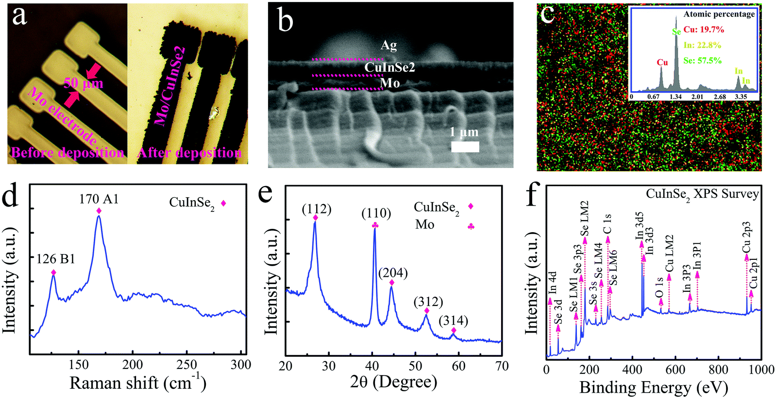
Fig. 1 shows the results of material characterizations. Device fabrication and characterization methods can be found in the Experimental section (ESI†). Fig. 1a presents the optical micrograph of the device. The left image in Fig. 1a shows the patterned Mo bottom electrode with a width of approximately 50 μm. The Mo electrode covered with the CIS film is shown in the right image in Fig. 1a. Only the areas covered with the Mo layer grew CIS, demonstrating a high materials utilization efficiency. The optical micrograph of the devices with a crossbar array configuration is shown in Fig. S7 (ESI†). The cross-section scanning electron microscopy (SEM) image is exhibited in Fig. 1b. The thickness of the CIS thin film was approximately 400 nm. The good adhesiveness exhibited in the image benefits electrical performances. To investigate the composition of the deposited CIS film, energy-dispersive X-ray spectroscopy (EDX) mapping is shown in Fig. 1c. The composition deviated slightly from the stoichiometric ratio (Cu:In:Se = 1:1:2).34 Atomic percentages of Cu and In are lower than the stoichiometric ratio (25%), meanwhile, a slightly high content of Se was obtained. The surface topography of the CIS is shown in Fig. S8 (ESI†). The CIS grew into a flower-like shape consisting of small grains. Some tiny voids that slightly increased the film roughness were observed, which may benefit the device performance due to the formation of guided conductive filaments.35 To Further confirm the elements were distributed uniformly in the flower-like shape grain. The zoom-in SEM image and EDX mapping are shown in Fig. S9 (ESI†). It can be found that the three elements were distributed uniformly in the grain.
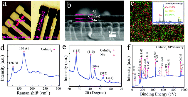 |
| | Fig. 1 Materials characterizations on the Ag/CIS/Mo device. (a) Optical micrograph of the device. (b) Cross-section SEM image of the device with a sandwich structure. (c) Surface composition EDX mapping of the deposited CIS thin film. The inset table presents the composition percentage (d) Raman spectrum of the deposited CIS. (e) GIXRD spectrum of the CIS/Mo. (f) Wide-scan XPS spectrum of the CIS thin film. | |
The Raman spectrum, Grazing Incidence X-ray Diffraction (GIXRD), and X-ray photoelectron spectrum (XPS) were employed to investigate the crystalline structure and surface chemical states of the CIS. The Raman spectrum is shown in Fig. 1d. The A1 vibration mode at 170 cm−1 and B1 vibration mode at 126 cm−1 were observed, corresponding to the tetragonal CIS structure.36 The GIXRD spectrum is shown in Fig. 1e. The characteristic peaks of tetragonal CIS at 26.6°, 44.1°, 52.4°, 59.7° corresponding to the (112), (204), (312), (314) planes respectively (JCPDS file: 03-065-4869) were found.37 The GIXRD confirms the crystalline structure of CIS, which is consistent with the Raman Spectrum result. Meanwhile, a relatively strong peak at 40.5° was observed. This peak is assigned to the (110) plane of the Mo electrode (JCPDS file: 01-089-5156). The surface chemical states of CIS were analysed by XPS. The wide-scan XPS spectrum of the CIS thin-film is exhibited in Fig. 1f. The characteristic peaks of Cu 2p, In 3d, and Se 3d can be observed. High-resolution XPS spectra of the three main elements are shown in Fig. S10 (ESI†). The Cu 2p peaks were located at 932.16 eV (2p3/2) and 952.09 eV (2p1/2) with the splitting orbital of 19.9 eV. This result confirms the oxidation state of Cu was +1.38 Meanwhile, the peak positions of In were 444.75 eV (3d5/2) and 452.3 eV (3d3/2), indicating the oxidation state of In+3. The Se 3d peak at 54.71 eV (3d5/2) and 55.53 eV (3d3/2) demonstrated that the valence state of Se was −2.38 Additionally, two impurity peaks at 284.69 eV and 531.6 eV indicated the contamination of carbon and oxygen due to the sample exposure to the atmosphere.38 Moreover, the permittivity ε of the CIS film was measured based on electrochemical impedance spectroscopy (EIS).39 The Nyquist plot and Bode plot are shown in Fig. S11 (ESI†), a permittivity ε of 7.9 was calculated based on the fitting parameters. The permittivity value slightly deviated from the reported value 13.6 ± 0.8 due to the different status of the material, including composition, crystalline status, fabrication process, etc.40 The materials characterization results confirm that the single CIS phase has been formed by the single-bath electrodeposition at room temperature. The electrodeposition can construct CIS-based memristor arrays, which shows remarkable advantages. The electrodeposition process is much cheaper than vacuum-based processes. In addition, electrodeposition is based on oxidation/reduction processes on the electrodes driven by electrical potentials. The film selectively grows on areas where charge exchange occurs. This method enables high utilization efficiency of materials because all reacted elements are utilized to form films.
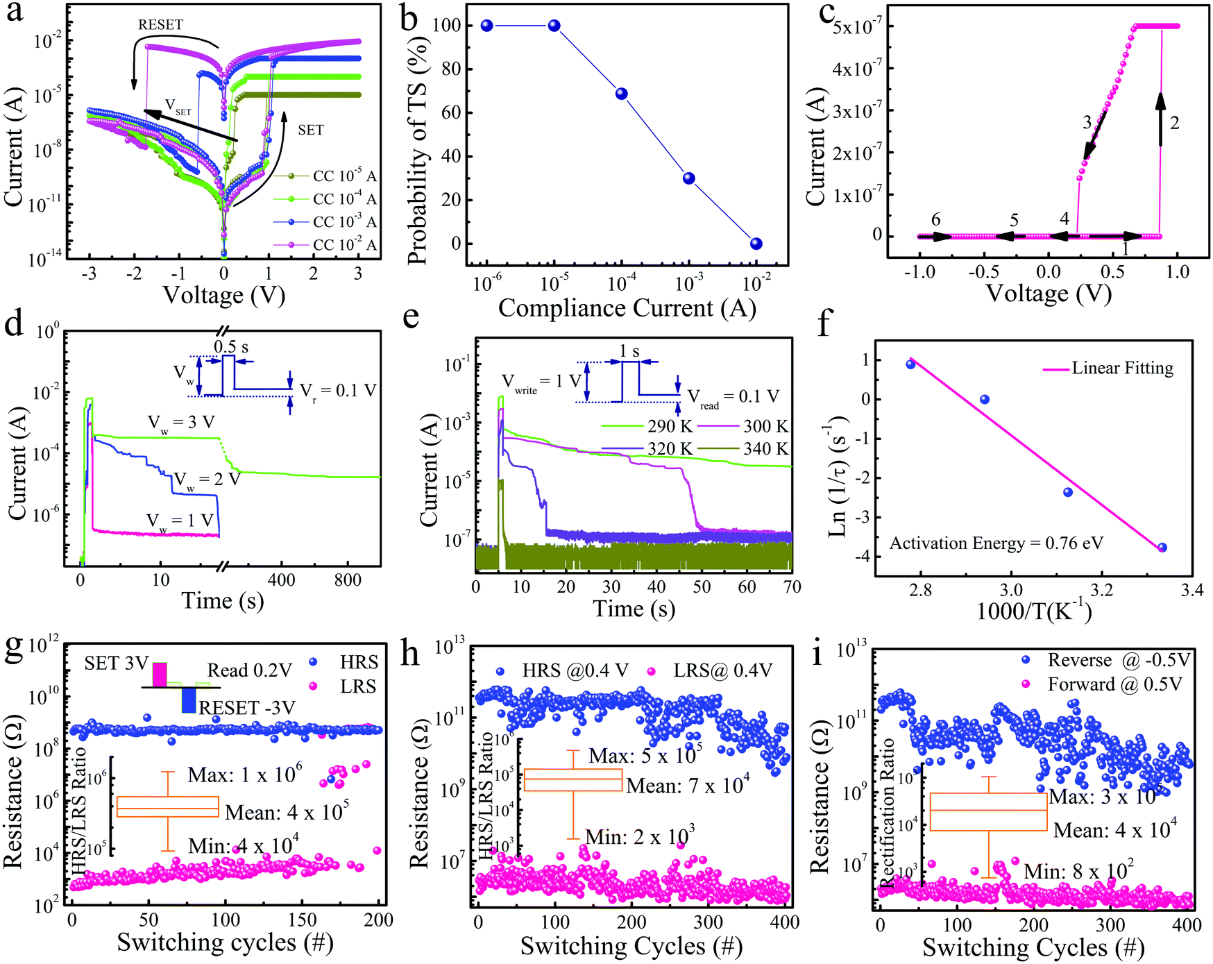
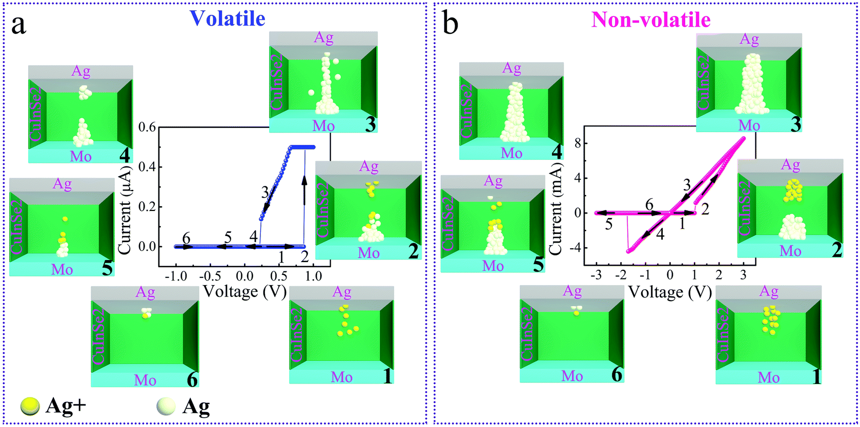
Systematic analysis of the resistive switching behaviours of the device is shown in Fig. 2. The direct current (DC) switching cycle test results of the device under different compliance currents (CCs) are shown in Fig. 2a, the voltage swept from −3 V to 3 V. The pristine device showed high resistance. When the voltage swept from 0 V to 3 V, the current abruptly increased under the voltages of approximately 0.9 V. The device switched from the original HRS to LRS, corresponding to a SET process. As the voltage swept from 3 V to 0 V, the I–V curves under different CCs showed different characterizations. As the CC ≤ 10−4 A, the device switched back to the HRS spontaneously when the applied voltage stress was close to zero, demonstrating a signature feature of volatile TS performance.7 In comparison, the device switched back to the HRS under the negative region when higher CCs were applied. The result means that the LRS can be maintained after the voltage is removed and a negative voltage was required to RESET the device, indicating a non-volatile MS performance.7 Additionally, the RESET voltage shifted from positive to negative with the increase of CCs, demonstrating the transition from the volatile TS to the non-volatile MS. Fig. 2b exhibits the probability for volatile TS as a function of CCs. The device can be switched between volatile TS and non-volatile MS modes by controlling the CCs. Note that the resistive switching behaviour is ascribed to the formation and rupture of Ag conductive filaments, which is discussed in detail in the mechanism discussion part. The transition between volatile TS and non-volatile MS is due to the controllable lifetime of conductive filaments. Moreover, I–V curves and RESET voltage changes over the different thicknesses of CIS layers are shown in Fig. S12 (ESI†). Under the same voltage stress, devices evolved from non-volatile to volatile characteristics when increasing the thickness of CIS, which is attributed to the different accumulations features of Ag atoms. Thicker and stronger conductive filaments were easier to form in thinner active layers, resulting in the RESET voltage shifting to negative regions. The non-volatile MS characteristics demonstrate the application for non-volatile memory. In the non-volatile mode, the HRS/LRS resistance distributions over 80 operation cycles (DC switching cycle test, the voltage swept from −3 V to 3 V) are shown in Fig. S13 (ESI†). An HRS/LRS ratio of 9 × 10⁶ (Mean value) was obtained. Notably, the device can provide diode-like volatile properties (Fig. 2c). When the voltage swept from 0 V to 1 V, the current abruptly increased under the voltages of approximately 0.9 V. The device switched from HRS to LRS, corresponding to a SET process. As the voltage swept from 1 V to 0 V, the LRS transformed to HRS under the voltages of approximately 0.2 V spontaneously, corresponding to a RESET process. This diode-like feature can be used as a selector that co-integrates with non-volatile memory devices to suppress sneak currents in crossbar arrays.41 Besides, the volatile properties indicate promising prospects as artificial neurons.
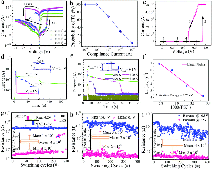 |
| | Fig. 2 Systematic analysis on resistive switching. (a) Typical I–V curve of the device under different compliance currents (CCs). (b) Probability for volatile TS as a function of CC, demonstrating the transition from volatile TS to non-volatile MS as increasing the CC. (c) Typical I–V curve of the device under a linear scale over the sweep voltage of −1 V to 1 V. (d) Retention time under different voltage amplitudes. (e) Retention time under different temperatures. (f) The Arrhenius plot of the retention time depending on the temperature. (g) Non-volatile switching under a pulsed-voltage operation. The operation voltage pulse was ±3 V with a duration of 1 s. The read voltage was 0.2 V. The duty cycle of the pulse was 50%. The box plot was based on the first 165 cycles. (h) The HRS/LRS resistance distribution over 400 switching cycles. The data was extracted from the result of the DC switching cycle test. The sweep voltage was −1 V to 1 V, the read voltage was 0.4 V. (i) The distribution of the device resistance under forward and reverse biasing over 400 switching cycles. The data was extracted from the result of the DC switching cycle test. After the device is SET to LRS, read the current at 0.5 V to get the forward resistance. After the device is RESET to HRS, read the current at −0.5 V to get the reverse resistance. The rectification ratio is (reverse resistance)/(forward resistance). | |
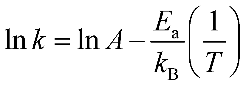
The retention time of the Ag/CIS/Mo device under different voltages and temperatures has been studied. To measure the retention time, a short pulse was used to switch the device to the LRS. Then, a small read voltage of 0.1 V was applied to monitor the resistance evolution. The influence of pulse voltage amplitudes on the retention time was studied with a pulse duration of 0.5 s, as shown in Fig. 2d. When using the operation-pulse voltage of 1.0 V, the device went back to the HRS closely following the end of the pulse. In comparison, when the voltage was 2.0 V, the retention time extended to approximately 17 s. More interestingly, the retention time was significantly extended when the pulse voltage amplitude was 3.0 V. As shown in Fig. S14 (ESI†), the LRS can be maintained for over 10,000 s when a pulse voltage of 3.0 V with a pulse duration of 1 s was applied, demonstrating non-volatile switching characteristics.42 This is because the higher voltage and longer pulse duration can induce thicker and stronger conductive filaments due to more Ag atoms being pumped into the active layer.43 Those stable Ag conductive filaments have a long lifetime and led to a long retention time. Fig. 2e shows the retention time under different temperatures. The retention time decreased with the increase of temperatures. This is due to the increased mobility of Ag atoms at higher temperatures.44 Hence, the conductive filaments are easier to rupture and lead to the resistance states transition, which is consistent with previously reported results.45 The Arrhenius plot of the relaxation time vs temperature is shown in Fig. 2f. The Arrhenius equation is used to analyse the relationship between rate constants and temperature. Here, it is used to investigate the minimum energy of molecules reaction, which is related to the interaction of Ag atoms and host materials.46 The Arrhenius equation is shown below:
| |  | (1) |
where
k is the rate constant that equals 1/
τ;
τ is the retention time of LRS.
A represents the pre-exponential factor,
kB represents the Boltzmann constant.
Ea represents the activation energy.
T represents the temperature. Taking a natural logarithm on the previous
eqn (1) gives the
eqn (2):
| | 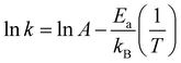 | (2) |
Eqn (2) was used to calculate the activation energy in the material system.
47 The fitting result matched well with experimental results (
Fig. 2f). The activation energy was 0.76 eV that is higher than those in SiO
xN
y:Ag (0.27 eV) and Ag/silk (0.52 eV).
45 The activation energy is related to the energy barrier of Ag diffusion, which may benefit the stability of the device. The above results demonstrate that the device can be modulated between the volatile and non-volatile switching models.
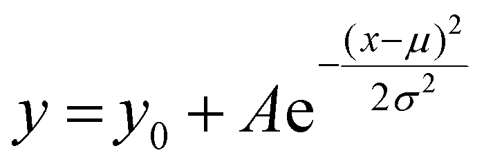
The endurance and stability of the device were investigated on both non-volatile and volatile switching models. For the non-volatile MS model, to mimic the voltage stresses applied on memory devices in practical applications, the resistance distribution under pulsed-voltage operation was carried out, as shown in Fig. 2g. The device was operated normally for around 165 cycles, giving an HRS/LRS ratio of 4 × 10⁵ (the mean value over 165 cycles). Then, abnormal resistive switching behaviours showed up, including invalid SET/RESET operation (the storage window was ≈ 0) and a small HRS/LRS ratio (approximately 100). The device degradation was due to the heat damage over the switch operation. As can be seen in Fig. 2g, the device was stuck in HRS after a few hundred cycles, which resulted in resistive switching failure. The CIS decomposes at a temperature higher than 600 K, indicating relatively low stability.48 During the pulsed operation process, the generated heat will be accumulated. The heat may damage the structure of the CIS film, which hinders the diffusion of Ag atoms, and the device cannot switch to LRS. Ma et al. reported that repeated switching operation can cause phase segregation in the active layer, resulting in resistive switching failure by stuck-in-HRS, which is similar here.49 There is still room to improve the endurance of the device for practical application. Future work is necessary to improve the device endurance for practical applications, such as the electronic packaging process (prevent the damage of humidity and oxygen), optimization of the active layer (such as thickness, roughness, crystal phase, etc.), heat management of the device, and adjusting the device structure. For the volatile TS model, Fig. S15 (ESI†) exhibits the DC switching cycle test for 400 operation cycles. The sweep voltage was from −1 V to 1 V. The distribution of LRS and HRS is shown in Fig. 2h, the read voltage was 0.4 V. The overall HRS/LRS ratio was 7 × 10⁴ (mean value over 400 cycles). No obvious degradation was observed for the first 250 cycles. When further operating the device, the device degenerated gradually, but it still can hold the HRS/LRS ratio of 1.5 × 10⁴ (the mean value of the last 20 cycles). Moreover, the switching speed was tested, as shown in Fig. S16 (ESI†). A switching speed of 400 μs was obtained. Fig. S17 (ESI†) shows the distribution of SET and RESET voltages. The results were fitted with the Gaussian equation eqn (3).
| |  | (3) |
where
A is a constant,
σ is the standard deviation and
μ represents the mean value. The
σSET/
μSET and
σRESET/
μRESET were 11% and 16%.
Fig. 2i shows the forward and reverse resistance at ± 0.5 V over 400 operation cycles, the results elaborate the stability of the volatile TS regarding the rectification characteristic. The rectification ratio was as high as 4.0 × 10
4. The selector with a high rectification ratio can efficiently alleviate sneak currents in crossbar memristors. A crossbar of 4 × 5 was fabricated in this paper. 12 of 20 devices can be operated over 100 cycles (DC switching cycle test, −1 V to 1 V). The yield was 60%. Fig. S18 (ESI
†) a–d exhibit the
I–
V curves of four typical devices. The LRS and HRS revolution over switching cycles are shown in Fig. S19 (ESI
†). The statistics analysis summary of the HRS/LRS ratio is shown in Table S1 (ESI
†). The mean ratio of HRS/LRS varied between 3.4 × 10
4 and 1.7 × 10
5. Indeed, the device yield in this paper is lower than wafer-scale integrated memristor arrays (a high yield of 98%).
50 Future work is needed to optimize the fabrication processes and device structures to realize practical applications.
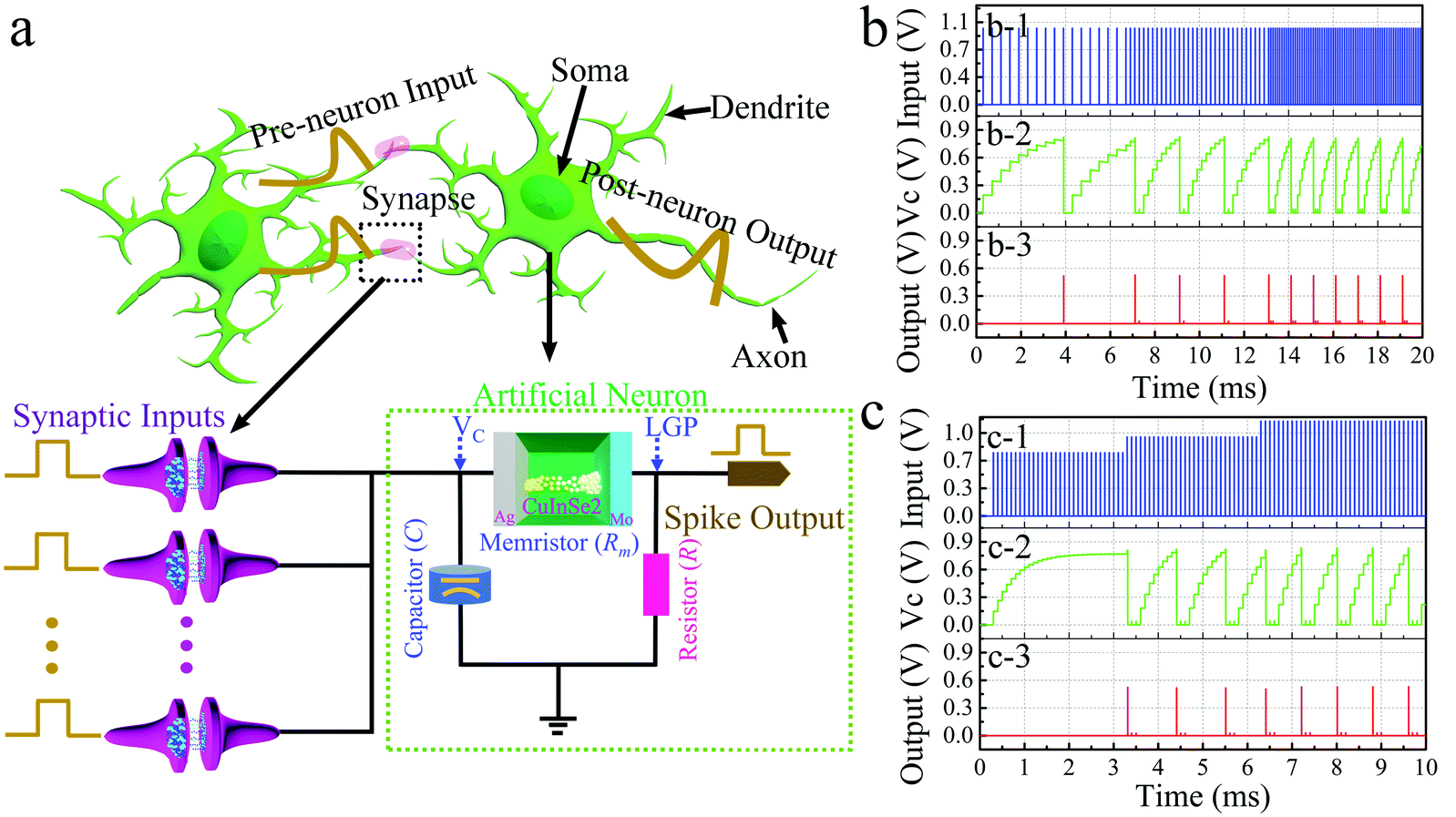
Human brain activities rely on neural networks consisting of ∼1015 synapses and ∼1011 neurons. The working principle of neural networks and the equivalent hardware circuit are shown in Fig. 3a. To mimic the functions of biological systems with artificial neural networks, the artificial neuron and artificial synapse are two main components. Artificial neurons generate spiking signals. Meanwhile, artificial synapses are connectors linking different neurons. The connection strength between neurons is determined by synapse weights (presented by the conductance of memristors).51 To realize neural functions by artificial devices, several neural models have been developed, including the Hodgkin–Huxley (HH) model, the integrate-and-fire (IF), and the leaky integrate-and-fire (LIF) model.51 Among them, the LIF model has been widely investigated due to its simplicity, reliability, and capturing the biological dynamics. The LIF neuron hardware is a combination of a “leaky” resistor term and a capacitor as shown in the schematic diagram of Fig. 3a. The LIF neuron model is described by eqn (4).52
| |  | (4) |
where
C is the capacitance of the capacitor. The capacitor receives charges from synaptic inputs.
53Vc(
t) is the voltage across the capacitor reflecting the dynamic change of membrane potential.
I(
t) is the current inputs from artificial synapses.
R is the series resistor.
Rm is the resistance of the volatile TS memristor. The
R +
Rm is the “leaky” term. In a neural network, neurons receive inputs from other neurons with various amplitudes and frequencies through synapses. The received charges are stored and accumulated in the capacitor. The accumulation of charges in the capacitor will increase the voltage attributed to the memristor (
M1). The SET process on the memristor occurs once the voltage applied on the memristor is higher than the SET voltage (
VSET). The voltage across the resistor
R4 increase drastically due to the resistance reduction of
M1. Thus, a spiking action will be generated and sent out.
52 Notably, the memristor used in the artificial neuron system should endow volatile properties so that it can go back to the initial state spontaneously after the spiking action.
9 More details about the working principle of LIF neurons can be found in the simulation method (ESI
†). The neuron responses under different input frequencies (with a fixed input voltage of 1 V) are shown in
Fig. 3b. Under a low frequency of 2.5 kHz, only 1 firing event happened with
VOUT ≈ 0.55 V. In comparison, the spiking frequency increase when the input frequency increased to 5 kHz. This was because the accumulation of charges in the
C1 capacitor was faster so that the memristor (
M1) can be switched to LRS more frequently. Meanwhile, as the input signal frequency further increased to 10 kHz, the frequency of output spike signals increased correspondingly, demonstrating an input-controlled spiking behaviour. On the other hand, the influence of input amplitudes (with a fixed frequency of 10 kHz) on neuron spiking performance has also been studied, as shown in
Fig. 3c. Neuron spiking was not generated under the input voltage of 0.8 V, because the charge accumulation was insufficient. Hence, the voltage on
M1 was not high enough to transform
M1 into LRS and generate an output spike. In comparison, stable neuron spiking signals were obtained when the input voltage amplitude was 1 and 1.2 V. This neuron spiking under different frequencies and amplitudes can mimic the actions in biological neuron systems to implement neuromorphic computing.
 |
| | Fig. 3 Schematic diagram of artificial neuron system and LIF neuron simulation results. (a) Diagram of biological artificial neuron system and the LIF neuron circuit. (b) The simulation of neural spiking response under different excitation frequencies. The b-1 shows the input signals with different frequencies. The b-2 shows the Vc under different input signals. The b-3 shows the output signals. (c) The simulation of neural spiking response under different excitation amplitudes. The c-1 shows the input signals with different amplitudes. The c-2 shows the Vc under different input signals. The b_3 shows the output signals. | |
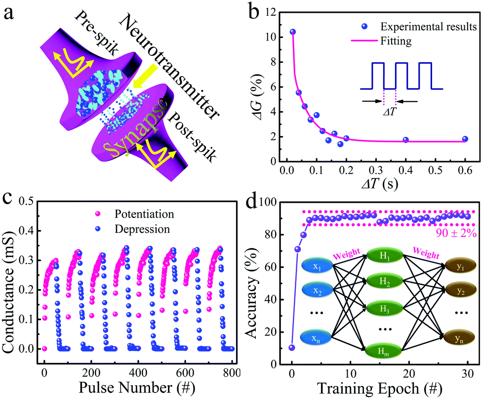
The synapse is crucial in biosystems, which have been investigated in the Ag/CIS/Mo device. The schematic diagram of a biological synapse is shown in Fig. 4a. Biological synapses connect neurons by controlling the absorption and extrusion of neurotransmitters (e.g. K+, Na+, Ca+), inducing plasticity reactions. Synaptic plasticity is the change of synaptic strength under external stimuli over time. This phenomenon is the foundation of memory and learning activities in human brains. In artificial neural networks, synaptic plasticity can be mimicked by the memristor with adjustable conductance.45 When two spikes occur in rapid succession, synaptic strength change by the second spike is enhanced, which is because that the interval time is too short for carriers to go back to their initial equilibrium states, namely paired-pulse facilitation (PPF). The plasticity of PPF is described by eqn (5).54
| |  | (5) |
where
G1 and
G2 are the conductance of the device after the first pulse and the second pulse, respectively. The PPF has been successfully simulated in the Ag/CIS/Mo device as shown in
Fig. 4b. The interval time between two pulses is denoted as Δ
T. The voltage amplitude was 1.0 V. Conductance (synaptic weight) changes depending on Δ
T were obtained. A typical current curve under two consecutive pulses is shown in Fig. S20 (ESI
†). The second pulse induced a larger conductance increase. Besides, the conductance returned to its original state gradually after the pulsed excitation. As the Δ
T increases from 20 ms to 600 ms, the conductance change decreased accordingly. A shorter interval between two stimuli can reinforce the memory effects, demonstrating agreement with biological synapses. This follows an exponential relationship described by
eqn (6).
55| |  | (6) |
where
c1,
c2, and
y0 are constants treated as fitting parameters.
τ1 and
τ2 are the fast and slow decaying terms, respectively. The fitting result is shown in
Fig. 4b (the pink line). The fast (
τ1) and slow (
τ2) decaying terms were 2.4 ms and 54.8 ms, respectively. Notably, long-term potentiation and depression behaviours under pulsed-voltage programming schemes were obtained as shown in
Fig. 4c. The conductance increased as the positive pulsed voltage was used, corresponding to the potentiation process. In comparison, the conductance decreased under negative pulses, indicating the depression process. To demonstrate the feasibility of the Ag/CIS/Mo artificial synapse for neuromorphic computing, the backpropagation algorithm for pattern recognition was simulated based on a three-layer artificial neural network (ANN). An 8 × 8 version of UCI Small images was employed as the training and test dataset.
56 The recognition accuracy reached over 90% after four training epochs as shown in
Fig. 4d. The pattern recognition accuracy was 90 ± 2% over 30 training epochs. The small accuracy fluctuation is due to the nature of the algorithm.
57 The simulation results claim that the potential and practicability of the artificial synapse for neuromorphic computing. Based on the above results, the versatile memristor can provide the functions of non-volatile memory, selectors, artificial neurons, and artificial synapses.
 |
| | Fig. 4 Artificial synaptic performance. (a) Schematic diagram of a synapse. (b) Experimental result of short-term synaptic PPF behavior. (c) The potentiation and depression behaviors of the device. The pulse amplitudes for potentiation and depression operations were +1 V and −1 V respectively. The pulse duration was 50 ms. The read voltage was 0.1 V. 50 consecutive pulses were applied for both potentiation and depression operations. (d) Simulations of backpropagation algorithm for UCI Small images recognition (images size is 8 × 8 version). | |
The resistive mechanism has been investigated systematically. To confirm that Ag dynamics dominated the resistive switching, the devices with different top electrodes, operation temperatures, and active layer thicknesses were studied. The electrical performance of the device with inert electrodes is shown in Fig. S21 (ESI†). No resistive switching was observed in the Mo/CIS/Mo device, confirming that Ag is essential for resistive switching. Furthermore, the LRS values of the Ag/CIS/Mo device under different temperatures were measured, as shown in Fig. S22 (ESI†). The resistance of LRS increased with the increase of temperature, which is the signature feature of metallic conducting, claiming that the metallic conductive filaments governed the LRS.58 The distribution of the RESET voltages of the device with different CIS thicknesses is shown in Fig. S23 (ESI†). The volatile and non-volatile transition with different active layers is investigated based on the Overdamped Langevin equation (ESI†). A thicker conductive is more likely induced in the device with thin active layers, demonstrating better stability. This theory explained the evolution phenomenon of non-volatile/volatile properties in devices with different CIS thicknesses. The thickness-modulated volatile/non-volatile memristor has been reported in the HfO2-based device, which is consistent with the results in this paper.15
Moreover, the electrical mechanism of the versatile memristor was investigated. Ohmic conduction was observed in memristor devices.59 The current value is proportional to the applied electric field. Ohm's law is described by eqn (7):60
where
σ represents the electrical conductivity.
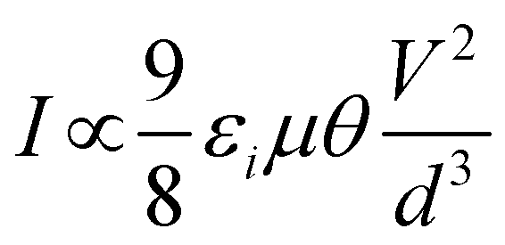
V is the applied voltage. The space-charge-limited-conduction (SCLC) and the Schottky emission are the two main conduction mechanisms found in the device. SCLC is described by the following
eqn (8).
61| |  | (8) |
where
I and
V are the current and voltage, respectively.
εi represents the permittivity.
θ represents the ratio of free and trapped charges.
μ represents electron mobility.
d is the thickness of the active layer in the memristor. The active layer of CIS is a p-type semiconductor.
37 A Schottky barrier was formed at the interface of metal electrodes and the active layer. Schottky emission describes the injection of electrons overcoming the energy barrier at metal–semiconductor junctions. The Schottky equation is shown below:
62| |  | (9) |
where
S is the device area;
k is the Boltzmann's constant;
m* represents the electron effective mass.
T describes the value of absolute temperature.
E represents the electric field across the active layer.
h represents Planck's constant.
ϕB represents the height of the junction energy barrier, and
ε is the permittivity.
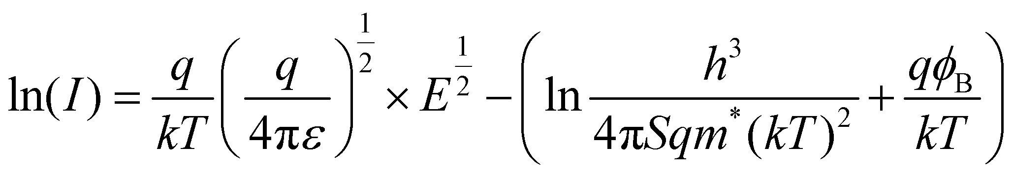
Eqn (9) can be transformed into
eqn (10).
| |  | (10) |
Then, the relationship between the applied voltage denoted by V and the electric field denoted by E is described by eqn (11)
| |  | (11) |
where
L is the thickness of the active layer. One can get the
eqn (12) from
eqn (10) and (11).
| |  | (12) |
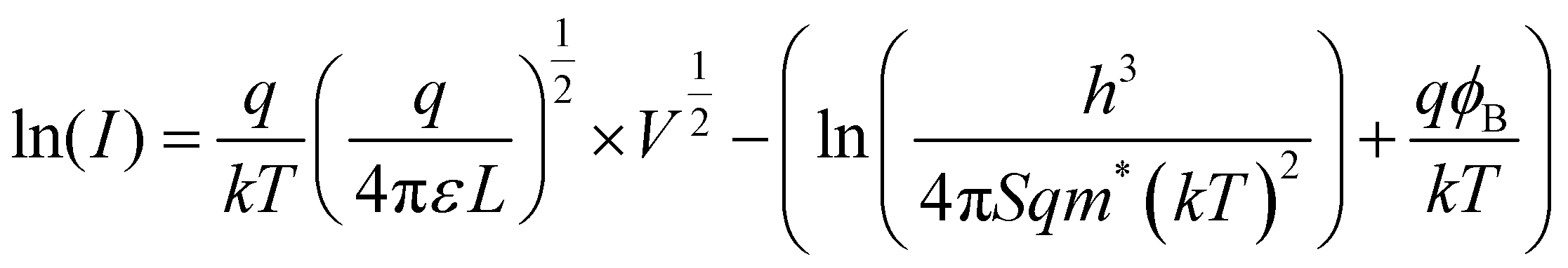
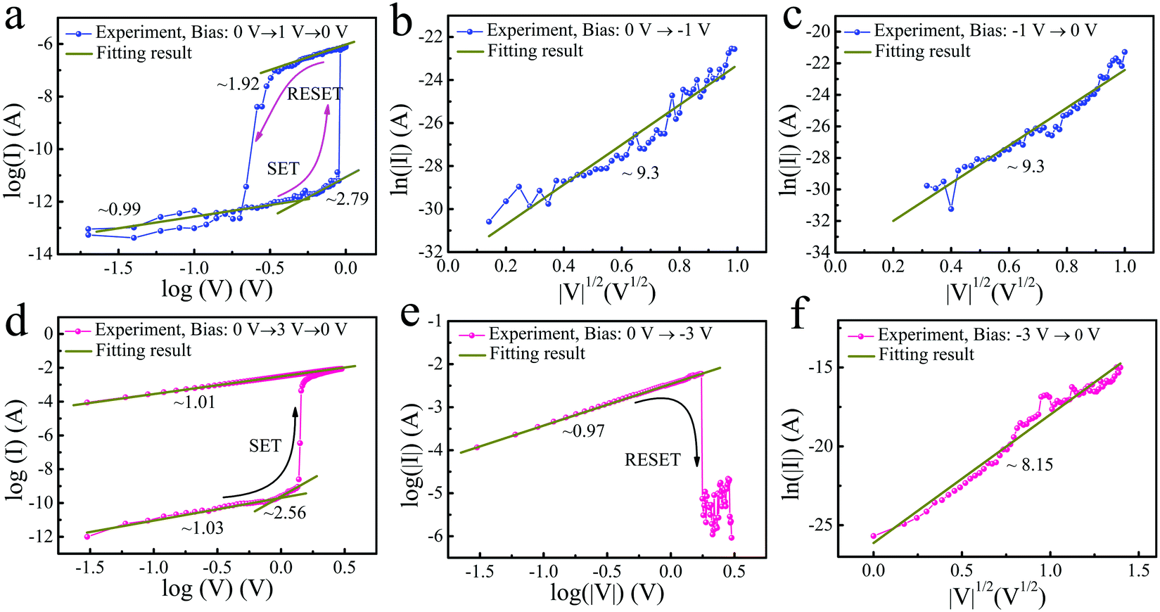
To confirm the conduction mechanism of Schottky emission, the fitting of ln (|I|)–V1/2 curves was carried out. A linear relationship can be expected since other variables in the equation are constants. Fig. 5 summarizes the fitting results to elaborate conduction mechanisms in the Ag/CIS/Mo device with the volatile and non-volatile performance. Fig. 5a shows the typical log (I)–log(V) curve under positive bias (0 V → 1 V → 0 V). When applying the voltage from 0 V to 1 V, the slope was 0.99, close to 1, at the low voltage region (0 V to approximately 0.6 V). The current increased proportionally with the increase of voltage, indicating Ohmic conduction. Afterward, the slope increased to 2.79 at a voltage range of approximately 0.6 V to 0.9 V. The concentration of injected electrons exceeded the equilibrium concentration, indicating the SCLC effects.17 Further increasing the voltage led to an abrupt current increase. This is due to the formation of Ag conductive filaments. After the device was switched to LRS, the slope was about 1.92 instead of 1.0. It did not follow Ohmic conduction due to the dynamic diffusion of Ag conductive filaments. When the voltage decreased to a certain value (approximately 0.2 V), the current decreased abruptly, demonstrating the rupture of Ag conductive filaments. When reversing the applied voltage, the device remained at the HRS. The ln (|I|)–V1/2 curves of the device at the negative region are shown in Fig. 5b and c. A linear fit was obtained, indicating the conduction mechanism was governed by Schottky emission.62 This is mainly attributed to the heterojunction of Ag/CIS. The work function of Ag and Mo are 4.26 eV and 4.60 eV, respectively.63 Meanwhile, the work function of CIS is about 4.85 eV.64 A schematic diagram of energy band alignment is shown in Fig. S24 (ESI†). The work function of CIS is close to that of Mo so that the barrier height at the CIS/Mo interface is small with a barrier height of 0.25 eV. In comparison, the gap between the work functions of CIS and Ag is relatively large with a barrier height of 0.59 eV. Therefore, the Schottky barrier height at the Ag/CIS interface is more significant in the device and determines the conduction mechanism at HRS. When a positive voltage was applied (positive voltage on Ag terminal while Mo terminal is grounded), the barrier height at the Ag/CIS interface increased. Thus, Schottky emission was difficult to occur. Hence, the Ohmic conduction dominates the conduction mechanism. Whereas, when a negative voltage was applied (negative voltage on Ag terminal while Mo terminal is grounded), the barrier height at the Ag/CIS interface decreased. In this case, electrons are easier to overcome the barrier, the Schottky emission dominates the conduction mechanism.
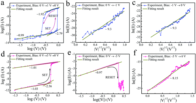 |
| | Fig. 5 Conduction mechanisms of the volatile TS and non-volatile MS in the Ag/CIS/Mo device. (a) log (I)–log(V) curve, the voltage swept from 0 V → 1 V → 0 V. (b) Ln(|I|)–|V|1/2 curve, the voltage swept from 0 V → −1 V. (c) Ln(|I|)–|V|1/2 curve, the voltage swept from −1 V → 0 V. (d) log(I)–log(V) curve, the voltage swept from 0 V → 3 V → 0 V. (e) Ln(|I|)–|V|1/2, the voltage swept from 0 V → −3 V. (f) Ln(|I|)–|V|1/2, the voltage swept from −3 V → 0 V. | |
For the non-volatile MS performance in the device, the log (I)–log(V) curve under positive bias (0 V → 3 V → 0 V) is shown in Fig. 5d. The slope over the low voltage region of 0 V to approximately 0.7 V was 1.03, indicating Ohmic conduction. Then, a slope of 2.56 showed up over the high voltage region (from approximately 0.7 V to 1.0 V), indicating the SCLC conduction model. Further increasing the voltage, a sharp current increase was observed due to the formation of Ag conductive filaments. For the LRS, the slope was 1.01 following the Ohmic conduction mechanism. The abrupt change was not found when the voltage swept from 3 V to 0 V. When reversing the voltage to the negative region, the slope was 0.97 in the low voltage region (0 V to approximately −1.7 V), which indicates the Ag conductive filament was stable and the device was still at LRS, as shown in Fig. 5e. When the absolute value of voltage exceeded 1.7 V, the current decreased suddenly. The conductive filament ruptured, and the device RESET to HRS. Fig. 5f shows the ln(|I|)–V1/2 curve as the voltage sweeps from −3 V to 0 V. The linear behaviour demonstrated that the conduction mechanism was governed by Schottky emission.
To elaborate on the conductivity evolution of the Ag/CIS/Mo device under different voltages, schematic diagrams of the resistive switching mechanism are shown in Fig. 6. Based on the above discussion, the dynamics of Ag conductive filaments are responsible for the resistance switching. Additionally, the volatile and non-volatile behaviours are due to the different stability of conductive filaments, which are determined by voltage stress.43 For volatile resistive switching, as shown in Fig. 6a, Ag atoms from the top electrode are oxidized into Ag+ under positive voltages (Fig. 6a1). This is described by eqn (13).58
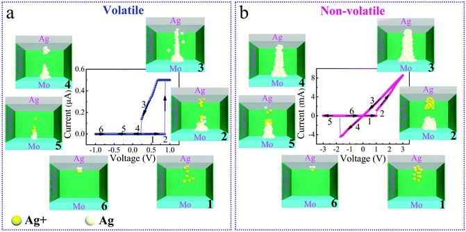 |
| | Fig. 6 Illustration diagram of the volatile/non-volatile resistive switching. (a) Mechanism of conductive filament evolution for the volatile TS behaviour. (b) Mechanism of conductive filament evolution for the non-volatile MS behaviour. | |
The ionized Ag+ penetrates the CIS film and migrates to the Mo electrode under the force of the electrical field, as shown in Fig. 6a2. Then the Ag+ ions are reduced into Ag atoms, eqn (14):65
Conductive filaments connect the top and bottom electrodes will form when sufficient Ag atoms are accumulated in the active layer as shown in Fig. 6a3. The resistance of the device will decrease suddenly owing to the high-conductive Ag filament. However, the conductive filament is relatively slim and unstable, resulting in filament rupture due to the minimization of filament surface energy when the applied bias is small,7 as shown in Fig. 6a4. When a reversed voltage is applied to the device, it remains at HRS since the inert Mo electrode cannot induce conductive filaments (Fig. 6a5 and a6). Thus, the device shows volatile TS characterizations.
With a higher operational voltage, more Ag atoms are oxidized into ions and then reduced into atoms, as shown in Fig. 6b1 and b2. Hence, the conductive filament is thicker and stronger, as shown in Fig. 6b3 and b4. The stable filaments do not break until the reversed voltage reaches a certain value. Ag atoms will be oxidized into Ag+ under negative voltages, inducing the dissolution of conductive filaments and the transition from LRS to HRS (Fig. 6b5). As the negative voltage is further applied, the residual Ag atoms in the active layer will be further dissolved and the device recovers to the initial condition (Fig. 6b6). Thus, the device shows non-volatile MS behaviours. The versatile memristor with the adjustable retention time enables multi-functions for memory and computation.
3. Conclusions
In summary, a versatile memristor (Ag/CIS/Mo) array covering multiple functions was developed. Non-volatile functionalities with a storage window of 4.0 × 10⁵ and a retention time of 10,000s were obtained, indicating the application of non-volatile memory. Besides, the Ag/CIS/Mo device showed diode-like volatile functionalities with a storage window of 7.0 × 10⁴ and a rectification ratio of 4.0 × 10⁴. The high rectification ratio can be used as selectors to suppress sneaky currents in memristor arrays. The device can be operated stably over 400 cycles, ensuring the mean HRS/LRS ratio of over 104. The leaky integrate-and-fire (LIF) neuron model based on the device has been studied, demonstrating potential as artificial neurons. Furthermore, the short-term synaptic PPF and long-term potentiation/depression performances were obtained in the same device. The image recognition simulation with the accuracy of 90 ± 2% was achieved, indicating the practicability of the artificial synapse for neuromorphic computing. A versatile memristor taking the multiple roles of non-volatile memory, selectors, artificial synapses, and artificial neurons will provide many advantages regarding circuit simplification, fabrication processes, and manufacturing costs. The devices with different top electrodes, operation temperatures, active layer thicknesses, and conduction mechanisms were investigated to reveal the resistive switching mechanism. It has been confirmed that the volatile/non-volatile bifunctional resistive switching is attributed to the dynamics of Ag atoms. Moreover, this work presents a novel bottom-up approach to fabricate crossbar array structure, where the CIS was grown locally by electrodeposition to form a patterned active layer. This method can potentially decrease manufacturing costs and achieve high utilization efficiency of materials. The results will promote the development of advanced data storage and neuromorphic computing systems in terms of the physical resistive mechanism and device fabrication.
Author contributions
Tao Guo: conceptualization, investigation, roles/writing – original draft, data curation. Kangqiang Pan: software. Yixuan Jiao, investigation. Bai Sun methodology. Cheng Du: investigation. Zuolong Chen: review & editing. Joel P. Mills: review & editing. Xiaoye Zhao: investigation. Lan Wei: conceptualization, review. Y. Norman Zhou: supervision. Yimin A. Wu: supervision, review, editing. All authors participated in the analysis and discussions of the results.
Conflicts of interest
There are no conflicts to declare.
Acknowledgements
This research was supported by the Natural Sciences and Engineering Research Council of Canada (NSERC) (RGPIN-2020-05903, GECR-2020-00476) and Canada Research Chairs (CRC) Programs.
Notes and references
- Q. Xia, M. D. Pickett, J. J. Yang, X. Li, W. Wu, G. Medeiros-Ribeiro and R. S. Williams, Adv. Funct. Mater., 2011, 21, 2660–2665 CrossRef CAS.
- S. Pi, C. Li, H. Jiang, W. Xia, H. Xin, J. J. Yang and Q. Xia, Nat. Nanotechnol., 2019, 14, 35–39 CrossRef CAS PubMed.
- Z. Lv, Y. Wang, J. Chen, J. Wang, Y. Zhou and S.-T. Han, Chem. Rev., 2020, 120, 3941–4006 CrossRef CAS PubMed.
- W. Huang, X. Xia, C. Zhu, P. Steichen, W. Quan, W. Mao, J. Yang, L. Chu and X. Li, Nano-Micro Lett., 2021, 13, 85 CrossRef CAS PubMed.
- Y. Wang, Y. Gong, L. Yang, Z. Xiong, Z. Lv, X. Xing, Y. Zhou, B. Zhang, C. Su, Q. Liao and S.-T. Han, Adv. Funct. Mater., 2021, 31, 2100144 CrossRef CAS.
- Z. Lv, Y. Wang, Z. Chen, L. Sun, J. Wang, M. Chen, Z. Xu, Q. Liao, L. Zhou, X. Chen, J. Li, K. Zhou, Y. Zhou, Y.-J. Zeng, S.-T. Han and V. A. L. Roy, Adv. Sci., 2018, 5, 1800714 CrossRef PubMed.
- W. Wang, M. Wang, E. Ambrosi, A. Bricalli, M. Laudato, Z. Sun, X. Chen and D. Ielmini, Nat. Commun., 2019, 10, 81 CrossRef CAS PubMed.
- Y. Wang, Y. Gong, S. Huang, X. Xing, Z. Lv, J. Wang, J.-Q. Yang, G. Zhang, Y. Zhou and S.-T. Han, Nat. Commun., 2021, 12, 5979 CrossRef CAS PubMed.
- R. Wang, J.-Q. Yang, J.-Y. Mao, Z.-P. Wang, S. Wu, M. Zhou, T. Chen, Y. Zhou and S.-T. Han, Adv. Intell. Syst., 2020, 2, 2000055 CrossRef.
- Z. Lv, Y. Zhou, S.-T. Han and V. A. L. Roy, Mater. Today, 2018, 21, 537–552 CrossRef CAS.
- R. Midya, Z. Wang, S. Asapu, X. Zhang, M. Rao, W. Song, Y. Zhuo, N. Upadhyay, Q. Xia and J. J. Yang, Adv. Intell. Syst., 2019, 1, 1900084 CrossRef.
- M. J. Yu, K. R. Son, A. C. Khot, D. Y. Kang, J. H. Sung, I. G. Jang, Y. D. Dange, T. D. Dongale and T. G. Kim, J. Mater. Res. Technol., 2021, 15, 1984–1995 CrossRef CAS.
- T. Liu, M. Verma, Y. Kang and M. Orlowski, Appl. Phys. Lett., 2012, 101, 073510 CrossRef.
-
Y. Shi, C. Pan, V. Chen, N. Raghavan, K. L. Pey, F. M. Puglisi, E. Pop, H.-S. P. Wong and M. Lanza, in 2017 IEEE International Electron Devices Meeting (IEDM), IEEE, San Francisco, CA, USA, 2017, p. 5.4.1–5.4.4.
- H. Abbas, Y. Abbas, G. Hassan, A. Sergeevich Sokolov, Y.-R. Jeon, B. Ku, C. Jung Kang and C. Choi, Nanoscale, 2020, 12, 14120–14134 RSC.
- Y. Li, P. Yuan, L. Fu, R. Li, X. Gao and C. Tao, Nanotechnology, 2015, 26, 391001 CrossRef PubMed.
- H. Abbas, A. Ali, J. Jung, Q. Hu, M. R. Park, H. H. Lee, T.-S. Yoon and J. Kang, Appl. Phys. Lett., 2019, 6 Search PubMed.
- G. Du, H. Li, Q. Mao and Z. Ji, J. Phys. D: Appl. Phys., 2016, 49, 445105 CrossRef.
- F. M. Simanjuntak, S. Chandrasekaran, B. Pattanayak, C.-C. Lin and T.-Y. Tseng, Nanotechnology, 2017, 28, 38LT02 CrossRef PubMed.
- S. J. Yoon, J.-H. Ryu, M. Ismail, Y.-C. Chen, Y.-F. Chang, M. J. Yun, H.-D. Kim and S. Kim, Appl. Phys. Lett., 2019, 115, 212102 CrossRef.
- N. He, L. Tao, Q. Zhang, X. Liu, X. Lian, X. Wan, E.-T. Hu, L. He, Y. Sheng, F. Xu and Y. Tong, ACS Appl. Nano Mater., 2021, acsanm.0c03180 Search PubMed.
- I. Michelakaki, P. Bousoulas, S. Stathopoulos, N. Boukos and D. Tsoukalas, J. Phys. D: Appl. Phys., 2017, 50, 045103 CrossRef.
- S. Munjal and N. Khare, Nanotechnology, 2021, 32, 185204 CrossRef CAS PubMed.
- X. Lian, X. Shen, J. Fu, Z. Gao, X. Wan, X. Liu, E. Hu, J. Xu and Y. Tong, Electronics, 2020, 9, 2098 CrossRef CAS.
- H. Cho and S. Kim, Nanomaterials, 2020, 10, 1709 CrossRef CAS PubMed.
- G. U. Kamble, A. V. Takaloo, A. M. Teli, Y. J. Kim, P. Sonar, T. D. Dongale, D. Kim and T. W. Kim, J. Alloys Compd., 2021, 872, 159653 CrossRef CAS.
- T. D. Dongale, A. C. Khot, A. V. Takaloo, K. R. Son and T. G. Kim, J. Mater. Sci. Technol., 2021, 78, 81–91 CrossRef.
- A. C. Khot, T. D. Dongale, J. H. Park, A. V. Kesavan and T. G. Kim, ACS Appl. Mater. Interfaces, 2021, 13, 5216–5227 CrossRef CAS PubMed.
- A. A. Patil, S. V. Wagh, T. D. Dongale and D. Kim, Mater. Lett., 2020, 280, 128587 CrossRef CAS.
- T. D. Dongale, A. C. Khot, A. V. Takaloo and T. G. Kim, NPG Asia Mater., 2021, 13, 16 CrossRef CAS.
- Z. Wang, M. Rao, R. Midya, S. Joshi, H. Jiang, P. Lin, W. Song, S. Asapu, Y. Zhuo, C. Li, H. Wu, Q. Xia and J. J. Yang, Adv. Funct. Mater., 2018, 28, 1704862 CrossRef.
- D. Soltz, G. Dagan and D. Cahen, Solid State Ionics, 1988, 28, 1105–1110 CrossRef.
- L. Chernyak, K. Gartsman, D. Cahen and O. M. Stafsudd, J. Phys. Chem. Solids, 1995, 56, 1165–1191 CrossRef CAS.
- Y. Aida, V. Depredurand, J. K. Larsen, H. Arai, D. Tanaka, M. Kurihara and S. Siebentritt, Prog. Photovoltaics, 2015, 23, 754–764 CAS.
- Y. Sun, C. Song, J. Yin, X. Chen, Q. Wan, F. Zeng and F. Pan, ACS Appl. Mater. Interfaces, 2017, 9, 34064–34070 CrossRef CAS PubMed.
- C. Rincón and F. J. Ramírez, J. Appl. Phys., 1992, 72, 4321–4324 CrossRef.
- J. Lauth, J. Marbach, A. Meyer, S. Dogan, C. Klinke, A. Kornowski and H. Weller, Adv. Funct. Mater., 2014, 24, 1081–1088 CrossRef CAS.
- Y. Zhao, S. Yuan, D. Kou, Z. Zhou, X. Wang, H. Xiao, Y. Deng, C. Cui, Q. Chang and S. Wu, ACS Appl. Mater. Interfaces, 2020, 10 Search PubMed.
- J.-B. Jorcin, M. E. Orazem, N. Pébère and B. Tribollet, Electrochim. Acta, 2006, 51, 1473–1479 CrossRef CAS.
- P. W. Li, R. A. Anderson and R. H. Plovnick, J. Phys. Chem. Solids, 1979, 40, 333–334 CrossRef CAS.
- D. Liu, H. Cheng, G. Wang, X. Zhu and N. Wang, J. Appl. Phys., 2013, 114, 154906 CrossRef.
- Z. Lv, M. Chen, F. Qian, V. A. L. Roy, W. Ye, D. She, Y. Wang, Z.-X. Xu, Y. Zhou and S.-T. Han, Adv. Funct. Mater., 2019, 29, 1902374 CrossRef.
- H. Sun, Q. Liu, C. Li, S. Long, H. Lv, C. Bi, Z. Huo, L. Li and M. Liu, Adv. Funct. Mater., 2014, 24, 5679–5686 CrossRef CAS.
- D. C. Schlößer, K. Morgenstern, L. K. Verheij, G. Rosenfeld, F. Besenbacher and G. Comsa, Surf. Sci., 2000, 465, 19–39 CrossRef.
- Z. Wang, S. Joshi, S. E. Savel’ev, H. Jiang, R. Midya, P. Lin, M. Hu, N. Ge, J. P. Strachan, Z. Li, Q. Wu, M. Barnell, G.-L. Li, H. L. Xin, R. S. Williams, Q. Xia and J. J. Yang, Nat. Mater., 2017, 16, 101–108 CrossRef CAS PubMed.
- K. J. Laidler, J. Chem. Educ., 1984, 61, 494 CrossRef CAS.
- F. Jensen, Qual. Reliab. Eng. Int., 1985, 1, 13–17 CrossRef.
- S. M. Chauhan, S. H. Chaki, M. P. Deshpande, T. J. Malek and J. P. Tailor, Int. J. Thermophys., 2018, 39, 18 CrossRef.
- Y. Ma, P. P. Yeoh, L. Shen, J. M. Goodwill, J. A. Bain and M. Skowronski, J. Appl. Phys., 2020, 128, 194501 CrossRef CAS.
- S. Chen, M. R. Mahmoodi, Y. Shi, C. Mahata, B. Yuan, X. Liang, C. Wen, F. Hui, D. Akinwande, D. B. Strukov and M. Lanza, Nat. Electron., 2020, 3, 638–645 CrossRef CAS.
- R. Yang, H.-M. Huang and X. Guo, Adv. Electron. Mater., 2019, 5, 1900287 CrossRef.
- H.-M. Huang, R. Yang, Z.-H. Tan, H.-K. He, W. Zhou, J. Xiong and X. Guo, Adv. Mater., 2019, 31, 1803849 CrossRef PubMed.
- Z. Wang, M. Rao, J.-W. Han, J. Zhang, P. Lin, Y. Li, C. Li, W. Song, S. Asapu, R. Midya, Y. Zhuo, H. Jiang, J. H. Yoon, N. K. Upadhyay, S. Joshi, M. Hu, J. P. Strachan, M. Barnell, Q. Wu, H. Wu, Q. Qiu, R. S. Williams, Q. Xia and J. J. Yang, Nat. Commun., 2018, 9, 3208 CrossRef PubMed.
- W. Huang, P. Hang, Y. Wang, K. Wang, S. Han, Z. Chen, W. Peng, Y. Zhu, M. Xu, Y. Zhang, Y. Fang, X. Yu, D. Yang and X. Pi, Nano Energy, 2020, 73, 104790 CrossRef CAS.
- I. Valov, E. Linn, S. Tappertzhofen, S. Schmelzer, J. van den Hurk, F. Lentz and R. Waser, Nat. Commun., 2013, 4, 1771 CrossRef CAS PubMed.
-
D. Dua and C. Graff (2019). UCI Machine Learning Repository http://[http://archive.ics.uci.edu/ml]. Irvine, CA: University of California, School of Information and Computer Science.
- Y. van de Burgt, E. Lubberman, E. J. Fuller, S. T. Keene, G. C. Faria, S. Agarwal, M. J. Marinella, A. A. Talin and A. Salleo, Nat. Mater., 2017, 16, 6 CrossRef PubMed.
- Y. Yang, P. Gao, S. Gaba, T. Chang, X. Pan and W. Lu, Nat. Commun., 2012, 3, 732 CrossRef PubMed.
- Z. Lv, X. Xing, S. Huang, Y. Wang, Z. Chen, Y. Gong, Y. Zhou and S.-T. Han, Matter, 2021, 4, 1702–1719 CrossRef CAS.
- N. Croitoru, M. Lazarescu, C. Popescu, M. Telnic and L. Vescan, J. Non-Cryst. Solids, 1972, 8–10, 781–786 CrossRef CAS.
- S. Kim, H. Y. Jeong, S.-Y. Choi and Y.-K. Choi, Appl. Phys. Lett., 2010, 97, 033508 CrossRef.
- B. J. Choi, J. Zhang, K. Norris, G. Gibson, K. M. Kim, W. Jackson, M.-X. M. Zhang, Z. Li, J. J. Yang and R. S. Williams, Adv. Mater., 2016, 28, 356–362 CrossRef CAS PubMed.
- H. B. Michaelson, J. Appl. Phys., 1977, 48, 6 CrossRef.
- T. Maeda, W. Gong and T. Wada, Jpn. J. Appl. Phys., 2016, 55, 04ES15 CrossRef.
- Y. Yang and R. Huang, Nat. Electron., 2018, 1, 274–287 CrossRef.
Footnote |
| † Electronic supplementary information (ESI) available. See DOI: 10.1039/d1nh00481f |
|
| This journal is © The Royal Society of Chemistry 2022 |

 c,
Cheng
Du
a,
Joel P.
Mills
a,
Zuolong
Chen
a,
Xiaoye
Zhao
ad,
Lan
Wei
b,
Y. Norman
Zhou
c,
Cheng
Du
a,
Joel P.
Mills
a,
Zuolong
Chen
a,
Xiaoye
Zhao
ad,
Lan
Wei
b,
Y. Norman
Zhou