
 Open Access Article
 This Open Access Article is licensed under a
 Creative Commons Attribution 3.0 Unported Licence
Thermally-driven formation method for growing (quantum) dots on sidewalls of self-catalysed thin nanowires
Yunyan
Zhang
 *abd,
H. Aruni
Fonseka
c,
Hui
Yang
*e,
Xuezhe
Yu
b,
Pamela
Jurczak
b,
Suguo
Huo
f,
Ana M.
Sanchez
c and
Huiyun
Liu
b
*abd,
H. Aruni
Fonseka
c,
Hui
Yang
*e,
Xuezhe
Yu
b,
Pamela
Jurczak
b,
Suguo
Huo
f,
Ana M.
Sanchez
c and
Huiyun
Liu
b
aSchool of Micro-Nano Electronics, Zhejiang University, Hangzhou, Zhejiang 311200, China. E-mail: yunyanzhang@zju.edu.cn
bDepartment of Electronic and Electrical Engineering, University College London, London WC1E 7JE, UK
cDepartment of Physics, University of Warwick, Coventry CV4 7AL, UK
dDepartment of Physics, Paderborn University, Warburger Straße 100, Paderborn, 33098, Germany
eDepartment of Materials, Imperial College London, Exhibition Road, London SW7 2AZ, UK. E-mail: h.yang.14@ucl.ac.uk
fLondon Centre for Nanotechnology, University College London, WC1H 0AH, UK
First published on 4th February 2022
Abstract
Embedding quantum dots (QDs) on nanowire (NW) sidewalls allows the integration of multi-layers of QDs into the active region of radial p–i–n junctions to greatly enhance light emission/absorption. However, the surface curvature makes the growth much more challenging compared with growths on thin-films, particularly on NWs with small diameters (Ø < 100 nm). Moreover, the {110} sidewall facets of self-catalyzed NWs favor two-dimensional growth, with the realization of three-dimensional Stranski–Krastanow growth becoming extremely challenging. Here, we have developed a novel thermally-driven QD growth method. The QD formation is driven by the system energy minimization when the pseudomorphic shell layer (made of QD material) is annealed under high-temperature, and thus without any restriction on the NW diameter or the participation of elastic strain. It has demonstrated that the lattice-matched Ge dots can be grown defect-freely in a controllable way on the sidewall facets of the thin (∼50 nm) self-catalyzed GaAs NWs without using any surfactant or surface treatment. This method opens a new avenue to integrate QDs on NWs, and can allow the formation of QDs in a wider range of materials systems where the growth by traditional mechanisms is not possible, with benefits for novel NWQD-based optoelectronic devices.
New conceptsThis work developed a novel technique to grow QDs onto the sidewall of NWs, using thermally-driven mechanism. In the growth, the system energy minimization can drive the pseudomorphic shell layer into defect-free QDs when it is annealed under high-temperature. Thus, it is unlike the traditional QD growth methods and has no restrictions on the NW diameter or the participation of elastic strain. It has demonstrated that the lattice-matched Ge dots can be uniformly grown in a controllable way on the sidewalls facets of the thin (∼50 nm) self-catalyzed GaAs NWs without using any surfactant or surface treatment. This method is different from the traditional Stranski–Krastanov or Volmer–Weber growth modes, which opens a new avenue to integrate QDs on NWs. |
Introduction
Nanowires (NWs) have novel mechanical, optical and electronic characteristics that are not observed in thin films, for example operating as an optical cavity for light emitters and enhancing light absorption for photovoltaics.1–5 Hybrid structures, designed by integrating quantum dots (QDs) with NWs, further improves their performance compared with homogeneous NWs. QDs provide a unique semiconductor structure with fully quantised electronic states for the fabrication of both high-efficiency classical and non-classical photon emitters/absorbers. Examples include low threshold current density lasers with reduced sensitivity to temperature variation, trains of regularly spaced single photon emitters, and entangled photon pair sources.6–8Research on QD/NW integration has gained increasing attention in recent years. Especially, the ability to grow QDs on NW sidewalls can allow easy control of the thickness of shells beneath and above the QD layers, which is advantageous for sandwiching QDs into the intrinsic active region of radial p–i–n junctions. Besides, many optoelectronic devices such as lasers and intermediate band solar cells require multilayer QDs to obtain higher gain or light absorption.9 This can be achieved by growing multilayer QDs on the NW sidewalls, with many reports available on the realization of this type of structures, such as Ge QDs on Si NWs, MnAs QDs on InAs QDs, and In(Ga)As QDs on GaAs NWs.9–13 A majority of these studies are based on the strain-driven Stranski–Krastanov (SK) growth mode,9–14 although dot formation at the junction of branched NWs15 and as a result of phase separation16 have also been observed. The SK growth mode is responsible for the 2D to 3D transition in heteroepitaxial growth and it has been successfully applied in low-threshold lasers, light emitting diodes, and solar cells.6,17 However, the implementation of the SK growth mode on NWs faces significant challenges.
The SK growth mechanism occurs to relieve the strain energy of lattice mismatched hetero-epitaxy through the formation of islands. Thus, for example in the InAs/GaAs system, with 7.2% lattice mismatch between InAs and GaAs, InAs QDs are formed as follows. Initially, a complete two-dimensional InAs pseudomorphic wetting layer (WL) on the GaAs surface forms, followed by the growth of three dimensional InAs islands. The WL thickness depends on the nature of the system, thus above a critical thickness of the WL, the strain energy stored in the epilayer causes the surface morphology to change from 2-dimensional (2D) layer growth to an island mode (3D).
In the case of epitaxial growth on NWs, the NW can share strain caused by the lattice mismatch of the QD on its facets when the NW thickness is similar in size to the QD width.18,19 Therefore, QD growth on NWs requires a much thicker critical wetting layer thickness for island formation than that on a planar substrate.9,20 The presence of a thick WL interconnecting QDs on thinner wires can greatly degrade QD performance. It has been found that QDs form more readily on a thicker NW in comparison with a thinner one, because less material contributes to the wetting layer shell and more contributes to the formation of QDs.9 For very thin NWs, the growth may only follow the Frank–van der Merwe (FM) thin-film growth mechanism due to the good radial strain relaxation ability, which completely prevents the growth of QDs.21,22 It has been proposed that the critical diameter of a GaAs NW to form InAs QDs is larger than 120 nm.20
Moreover, the SK growth mode is very sensitive to surface orientation. Gold-catalysed NWs commonly exhibit {112} sidewall facets, which are generally favourable for the SK QD growth. However, these NWs are incompatible with Si-based electronics, as Au can be incorporated into Si substrates23,24 as well as NWs25,26 at levels of the order of 1015–1018 cm−3. In the case of Au-free NWs, such as the self-catalysed NWs, {110} sidewall facets are commonly observed in the NWs.27 Due to the non-favourable {110} surface, QDs do not form on these surfaces, and micrometer-sized triangular structures containing dislocations are commonly observed.28–31 To the best of our knowledge, there is just one report on successful QDs growth on {110} NWs sidewalls so far. This was achieved by modifying the NW surface using an AlAs layer prior to QDs growth.12 For QDs of nanometer size, a direct growth technique without complex surface treatment is preferred to simplify the growth procedure and avoid the degradation of QD performance by additional layers.
On the other hand, a NW's ability to facilitate defect-free integration of different material families can be used to combine material systems that are highly advantageous for enhancing the performance of existing devices, and also creating new applications.32 Especially, the integration between the two most powerful semiconductor groups, group IVs and group III–Vs, is particularly relevant for expanding the wealth of optical and electronic applications.33,34 For instance, the growth of GeSn QDs with a direct band gap can cover the working wavelength from near, middle to far infrared, which can be so important to infrared detection and illumination.35 The application covers from optical data communication, bio-detection, sensing, fire prevention, geography monitoring, atmosphere monitoring, and military defence and so on. So, it is very useful and linked to a large market.
In this article, we report the formation of lattice-matched Ge dots on self-catalysed thin GaAs nanowires by a thermally-driven mechanism, providing a novel approach to form high-quality QDs on the {110} NW sidewalls regardless of the NW size and free from the formation of wetting layers.
Results and discussion
GaAs core NWs with a diameter ∼50 nm were grown by self-catalyzed mode on Si substrates. These NWs exhibited dominantly zinc blende crystal structure and smooth {110} sidewalls dominating this NWs. Single twins were presents just at the very tip and bottom parts (see ref. 36 and 37 for more details on these same GaAs core NWs). A Ge shell, with a nominal thickness of ∼50 nm (calibrated according to thin-film growth rate), was then grown on the GaAs core NWs at three different temperatures. The morphology and crystal quality of these Ge/GaAs NWs were analysed by scanning electron microscopy (SEM) and transmission electron microscopy (TEM) imaging respectively (Fig. 1). When the Ge shell is grown at 450 °C, the {110} NW facets parallel to the growth direction form flat sidewalls (Fig. 1a). The occasional twin defects (indicated by red arrows in Fig. 1d) commonly observed at the tip and bottom of the GaAs core NW has no apparent influence on the morphology of the {110} sidewalls (Fig. 1d). The increase on Ge growth temperature to 500 °C results in nano-scale sidewalls roughness, giving a wavy appearance (Fig. 1b), as clearly observed in Fig. 1e. Further increase of the growth temperature up to 550 °C, causes the surface to roughen even further and large island-like features are form on NW sidewall surfaces (Fig. 1c and f). Energy-dispersive X-ray spectroscopy (EDX) was performed on these NWs to ascertain the elemental distribution. Fig. 1g correspond to the annular dark field image and As, Ga, and Ge elemental distribution in a NW with the Ge shell grown at 550 °C. As can be observed, both Ga and As maps agrees with a smooth sidewall of the GaAs core NWs, whilst the Ge elemental distribution corroborates that the sidewall roughness is mainly caused by the Ge shell grown at 550 °C. Despite different morphology, all the Ge layers grown with different temperatures copied the template of GaAs core NWs, adopting cubic crystal structure that is the same as Fig. 1h and i.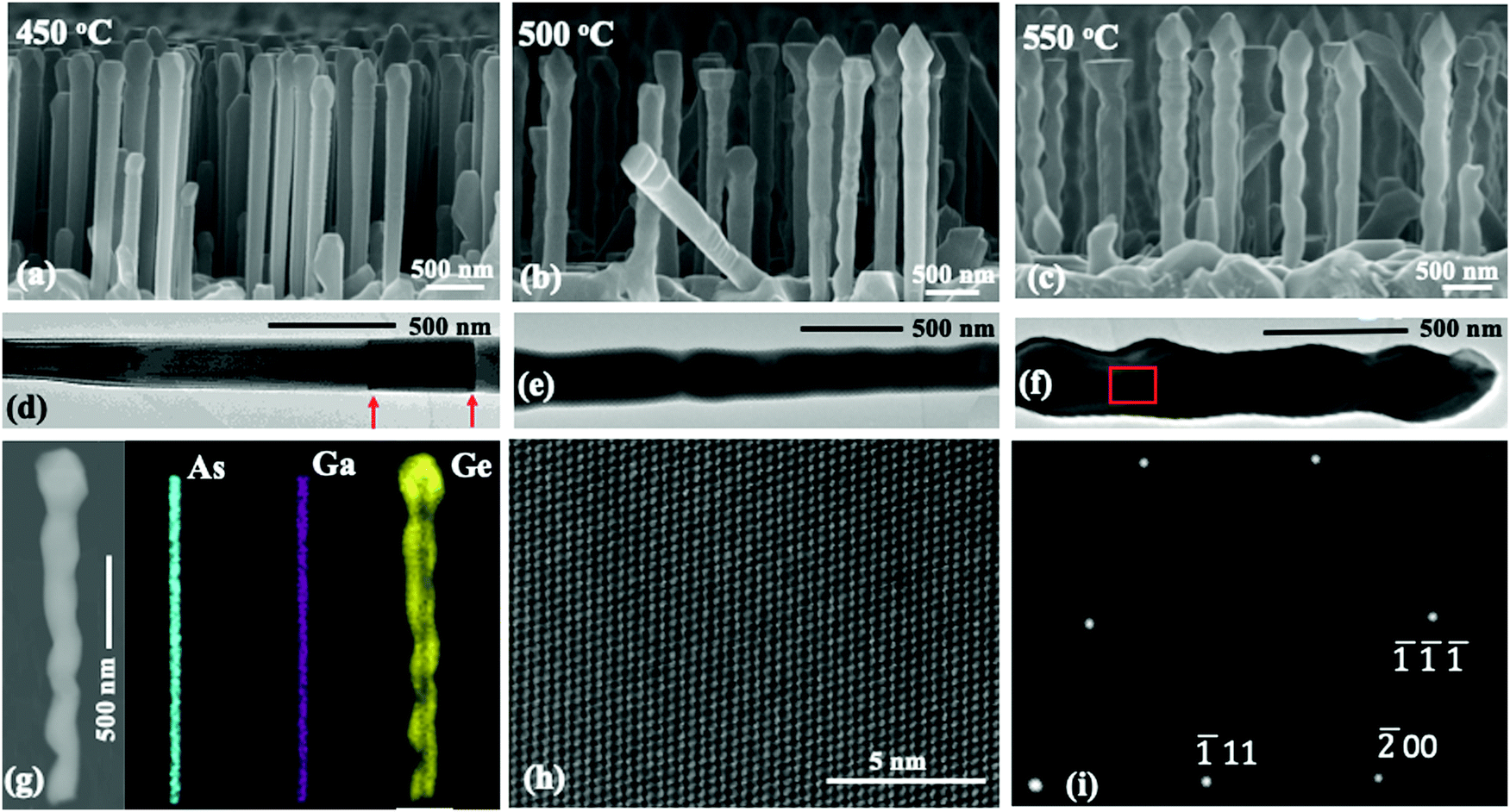 | ||
| Fig. 1 SEM and TEM images of GaAs NWs with a Ge shell. Ge shell grown at (a and d) 450 °C, (b and e) 500 °C, and (c and f) 550 °C. EDX maps of (g) a GaAs/Ge NW from (c) showing the distribution of As (cyan), Ga (magenta), and Ge (yellow) elements. (h) A representative atomic-resolution STEM image and (i) SAED pattern of the regions marked by a red square in (f). | ||
Large lattice mismatch between different materials results in structure defects and lattice distortion. Misfit accommodation can be also accommodated by the introduction of island or surface roughness, commonly associated to the large islands. Since the strain energy stored in mismatched layer increases usually with the square of the film thickness, and QDs formation is often considered as a form of strain relief. Thus, in SK growth mode, the formation of QD is a strain-driven process during which a 2D–3D transition occurs, with reorganization of the growing surface. In our system, the lattice mismatch between Ge and GaAs is <0.1%, ruling out strain-driven dots formation or surface roughness as revealed in Fig. 1f. Another factor that can lead to surface roughness is the presence of planar defects such as twins and stacking faults.38 Nevertheless, the island-like features also emerge in NWs segments which are stacking fault free, as presented in Fig. 1h and further confirmed by the selected area electron diffraction (SAED) pattern in Fig. 1i.
To elucidate the thermally-driven nature of the surface roughness and island-like features observed in our system when the entire NW is fully covered by Ge, theoretical calculations were performed using plane-wave pseudopotential density functional theory (DFT) formalism implemented in Vienna Ab initio Simulation Package (VASP).39 The structural stability is characterized by the crystal binding energy (ΔE), i.e. the system energy change before and after the Ge–GaAs integration, defined as:
| ΔE = EGaAs/2Ge − EGaAs − 2EGe |
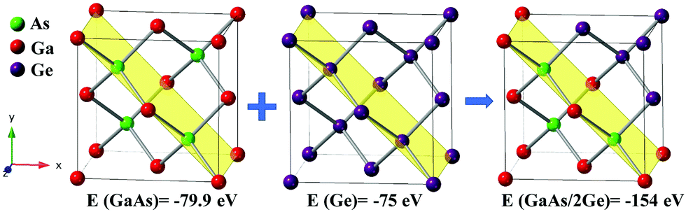 | ||
| Fig. 2 The crystal structure illustration of bulk GaAs, Ge and integrated GaAs/2Ge. The (110) lattice plane is showed in yellow. The total free energies are labelled per computational cell and the combined system is higher in energy by 8.28 meV Å−2. | ||
At a low temperature of 450 °C, 2-dimensional Ge thin-film growth (pseudomorphic mode) occurs under non-thermodynamic equilibrium conditions. Here, the Ge shell grows in a quasi-FM mode and the morphology is determined by a random but uniform deposition. When the growth temperature increases, so does the ad-atom mobility, enabling the ad-atoms diffuse to the energetically preferred state and the system reach an energetically more stable state. The atoms of the Ge film are more strongly coupled with each other than with the GaAs. This leads to 3D islands nucleation and growth directly on the surface of the NW, lowering the total system energy by allowing excess Ge to exist in an electronic state similar to bulk Ge. Thus, the substrate (i.e. NW) influences the overlayer not through strain but rather electronically.40 It needs to be mentioned that Erik Bakkers et al.41 also achieved uniform Ge shell growth on GaAs at quite high temperature, which could be due to the large growth rate of MOCVD that can greatly shorten the ad-atom diffusion length, which do not give them enough time to diffuse to the energetically preferred state.
As experimentally and theoretically demonstrated above, thermally-driven surface corrugation occurs in Ge/GaAs NWs. This phenomenon can provide a successful route to generate three-dimensional island on self-catalyzed NWs sidewalls. Thus, this is a very promising process to solve long-term difficulties in growing QDs on self-catalyzed small NWs. To demonstrate this, a Ge shell with a nominal thickness of ∼10 nm was grown on GaAs core NWs of smooth surfaces (Fig. 3a) at 350 °C.36 Since the shell growth at 450 °C produces highly uniform Ge shell (Fig. 1a), the growth temperature of 350 °C is beneficial for uniform shell layer formation. Then, the NWs was annealed at 600 °C for 15 min. The high temperature and long annealing time are beneficial for the Ge atoms to diffuse to the energetically preferred states, which is different from the samples shown in Fig. 1 with relative low temperatures and a continual growth environment that are disturbing the Ge ad-atom diffusion.
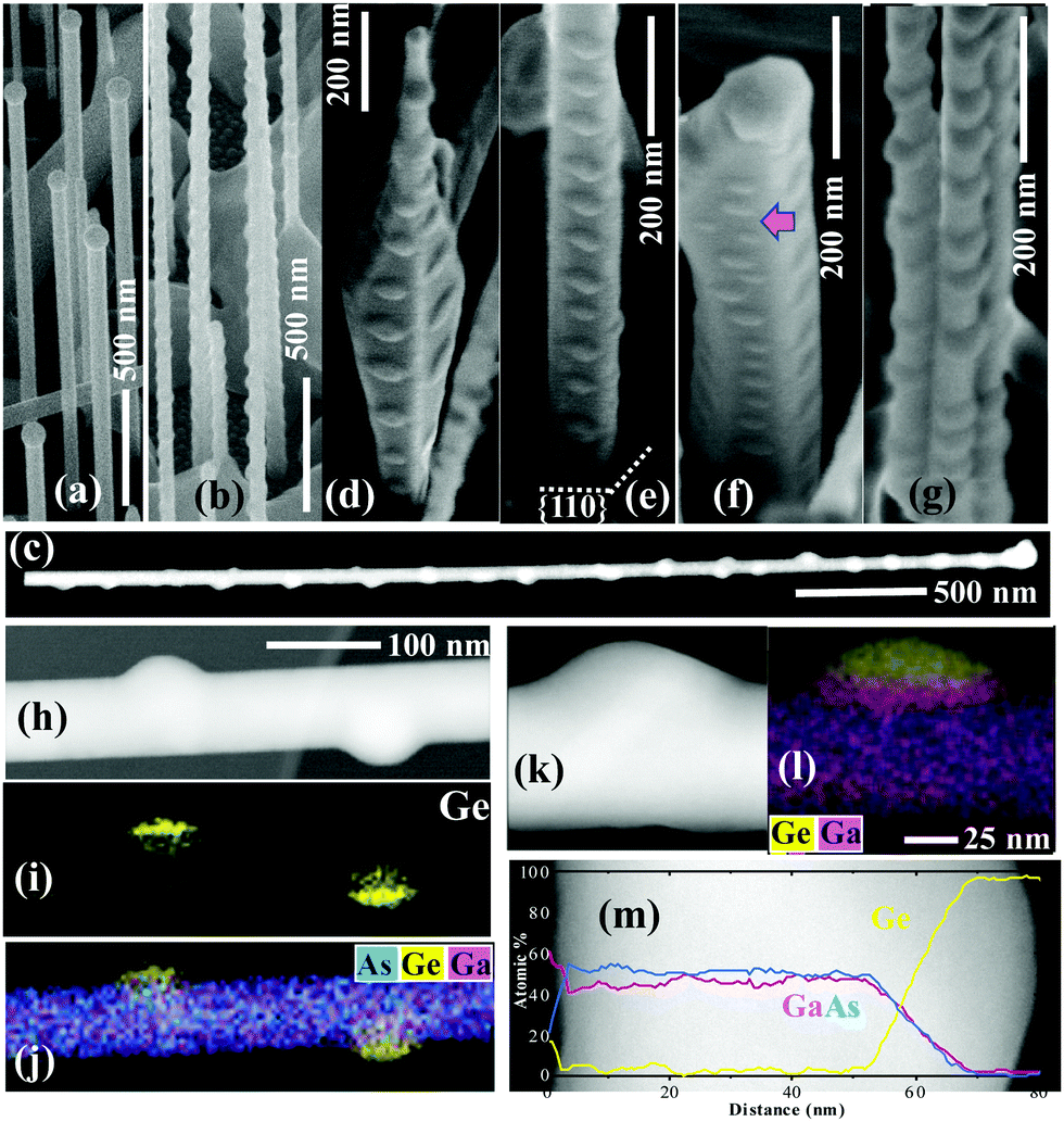 | ||
| Fig. 3 Ge dots grown on GaAs NWs. (a) SEM image of the core-only NWs. (b, d–f and g) are SEM images of the NWs with different facet sizes. Low magnification TEM shows (c) the entire NW and (h) a NW segment. EDX mapping of (i) Ge and (j) composition overlay of the NW segment shown in (g). (k) TEM and (l) corresponding EDX mapping of a Ge dot. (m) EDX line profile across the NW at a Ge dot. | ||
As can be seen in Fig. 3b and c, the GaAs NW surface is decorated with strings of dots from bottom to tip. These dots are preferentially located on the sidewall facets rather than on the corners, and the dot size is larger at the locations where the facet is wider, which is shown in Fig. 3d. If the side facet width is uniform along the NW length, the dots are relatively uniform in size and equally-distanced as can be seen in Fig. 3e. When the NW width is too large, it forms multiple dots (Fig. 3f). In thinner wires, the dots are spanning over to the two facets on the sides (Fig. 3g), which could be avoided by reducing the Ge deposition thickness. The EDX elemental maps demonstrate that the dots are mainly Ge in composition (Fig. 3h–j). A more detailed image and compositional analysis is shown in Fig. 3k and l. Here, it is clearly observed that Ge agglomerates to form dots on the NW sidewalls. Compositional line profile across the NWs in Fig. 3m shows that only the dot region of NWs has the detectable Ge; while the rest has the Ge signal at background level.
The high temperature annealing enhanced the Ge atoms mobility, beneficial for the minimization of system energy and gathering the Ge atoms into dots formation. Normally, the fast diffusion rate is beneficial for epi-growth, as the adatom can find the best location with the lowest energy.42 However, the film epi-growth temperature is normally not high enough to allow the material to diffuse freely. In contrast, the annealing temperature for Ge dot formation is much higher than the growth temperature, which gives the atoms very large energy to diffuse around, and leads to the growth of dots. The preferred location on the facet planes rather than the corner may be related to the small contact area of the dots with NWs and hence have a lower system energy. The increase in the dot size with the facet width is due to the larger facet being able to provide a larger amount of material for the formation of dots. Therefore, the dot size and density control can be achieved through the control of the material collection area, the material deposition amount and the annealing temperature. The larger material deposition amount and material collection area should yield larger dots, and the higher annealing temperature should reduce the dot density by enhancing the material diffusion.
It needs to be noted that Volmer–Weber (VW) growth mode can also lead to the formation of dots/clusters.43–45 However, the process is distinct from what we are using here. In the VW growth, the dot/cluster formation happens along with the growth, which means the material agglomeration already happens at the beginning of the growth; while in our growth, the 2D film was grown first and then annealed to form dots, in which the dot formation is after the material growth. Besides, in VW growth, the dot formation is commonly un-uniform and the shape is un-regular,43–45 which is in stark contrast to the uniform and round dots grown here (Fig. 3e, h and l) with good size controllability through material collection area (Fig. 3d). Besides, this method could be extended to synthesize other hybrid nanostructures. Different materials have different cohesive energies. In principle, materials of the same species tend to gather together as long as the energy added is enough to allow the atom diffusion inside the material, which is commonly called “compositional phase segregation”.46 For example, when growing InGaN with high In content, InN tends to gather together.46
Ge dots formed during the annealing process are epitaxial with respect to the core NWs as shown in Fig. 4a and b. The Ge dots atomic arrangement follows the zinc blende crystal structure observed in the GaAs. No dislocation was observed in the Ge dot or at the dots/core NW interface, confirmed by the strain map of the interface region shown in Fig. 4c. The strain map analysis using the geometric phase algorithm did not expose any detectable strain.47 When grown on a twin plane region (Fig. 4d), the dots follow completely the core NW crystal template, resulting in Ge dots contain also twin planes (Fig. 4e), without having any influence on their shape. We have not found any correlation between the dot formation and the presence of stacking faults, i.e. the defects did not act as preference site on the dot formation. The dots can be grown on twin planes (Fig. 4e), but without specific preference to grow on them. As can be seen in Fig. 3f and g, the dots are not pinned to twin planes despite being only a few nanometres away.
 | ||
| Fig. 4 TEM images of Ge dots. (a) Low-resolution image of a defect-free dot. (b) Atomic resolution image of the region shown in the blue region of (a). (c) Strain map in the horizontal direction of a dot. (d) A low magnification image of a dot containing two single twins. (e) Atomic resolution image of the region shown in (d). Low magnification image of dots grown (f) between and (g) next to two single twins. | ||
Conclusions
In summary, we have demonstrated for the first time the growth of strain-free dots on the {110} sidewalls of self-catalyzed thin NWs using the lattice-matched GaAs/Ge material system. The Ge dot formation on the GaAs NW is thermally-driven to minimize the system energy, which has much less restrictions on the requirement on the facet size than the SK growth mode. The dots can have relatively uniform size and inter-dot distance when grown on facets with a uniform width along the NW length. Benefitting from this growth mode, the dot formation does not need the assistance of the wetting layer that is commonly seen in SK dots, which can provide better quantum confinement. There is no observation of defects in these dots or at the dot/NW interface, and there is no direct correlation between the dot growth and the stacking faults of the core NW. This study provides an solution to the long-term issue of growing high-quality QDs onto the sidewall of NWs, and the strain-free growth mode can allow the construction of QDs from a much wider range of materials than traditional SK growth mode, allowing the development of novel QD devices. Besides, this also demonstrates the integration of high-quality group-IV materials with self-catalyzed III–V NWs in the form of QDs, which is promising for the construction of novel optical and electronic devices.Experimental section
NW growth
The self-catalyzed GaAs NWs were grown directly on p-type Si substrates by means of solid-source III–V molecular beam epitaxy (MBE).48 GaAs NWs were grown with a Ga beam equivalent pressure, V/III flux ratio, substrate temperature, growth duration and Be flux (equivalent to a nominal thin-film doping concentration) of 8.41 × 10⁻⁸ torr, 44, ∼630 °C, 1 hour and 0–1.28 × 1019 cm−3, respectively. After cooling down, the samples were transferred to the solid-source group-IV MBE for Ge growth using the ultrahigh-vacuum transfer chamber connecting the two MBE systems, which can keep a minimum contamination and surface damage of GaAs NWs when without exposing samples to air. The thick Ge shell (shown in Fig. 1) was grown at different temperatures (450, 500, and 550 °C) with a flux rate of 1.57 × 10⁻⁷ torr for 1 h. The Ge dots was grown by depositing 10 nm Ge at 350 °C and then annealed at 600 °C for 15 min.Density functional theory modeling
The starting points for our calculations were the experimentally determined structures of GaAs49 and Ge50 shown in Fig. 2. The model cells have been generated by projecting their primitive cubic cell on the lattice plane with Miller indices (h = 1, k = 1, l = 0) to accomplish combining the two-parental crystal. The crystal transformation and the images were generated using CrystalMaker.51 As a result, the number of atoms (see Table 1) are 16, 16 and 32 atoms in the lattice energy minimization simulations for GaAs, Ge and GaAs/2Ge, respectively. The blender interface is in ab plane in the transformed system.| No. of atom/unit cell | a | b | c | Free energy (eV) | |
|---|---|---|---|---|---|
| Ge | 16 | 5.76 | 8.15 | 8.15 | −79.90 |
| GaAs | 16 | 5.75 | 8.13 | 8.13 | −75.00 |
| GaAsGe | 32 | 5.75 | 8.13 | 16.26 | −154.00 |
For DFT calculations, Perdew–Burke–Ernzerhof (PBE) functional52 was used alongside dispersion correction of the Grimme's method (DFT-D3)53 for geometry optimization. Γ-Centered Monkhorst–Pack k-point meshes with 3 × 2 × 2 subdivisions were used for Ge and GaAs, while a 3 × 2 × 1 mesh was used for GaAs/Ge2 system because the combined crystal has a more anisotropic unit cell. The energy cutoff for the plane-wave basis set was set to 600 eV, and projector augmented-wave pseudopotentials54 were used. During the geometric optimization, the total energy was converged to within 1 meV per atom, and a force tolerance of 0.001 eV Å−1 was set for convergence of the ion positions to ensure accurate atomic positions and lattice parameters.
Scanning electron microscope (SEM)
The NW morphology was measured using Zeiss XB 1540 FIB/SEM and Zeiss Gemini 500 SEM systems.Transmission electron microscopy (TEM)
Simple mechanical transfer of the NWs onto lacey carbon support grids was used to prepare TEM specimens. The TEM measurements were performed using doubly-corrected ARM200F and Jeol 2100 microscopes, operating at 200 kV. EDX measurements were performed using an Oxford instruments 100 mm2 windowless detector installed within the ARM200F microscope.Conflicts of interest
There are no conflicts to declare.Acknowledgements
The authors acknowledge the support of Leverhulme Trust, EPSRC (grant no. EP/P000916/1 and EP/P000886/1), and EPSRC National Epitaxy Facility.References
- C. M. Lieber and Z. L. Wang, Functional nanowires, MRS Bull., 2007, 32, 99–108, DOI:10.1557/mrs2007.41.
- Y. Zhang, J. Wu, M. Aagesen and H. Liu, III–V nanowires and nanowire optoelectronic devices, J. Phys. D: Appl. Phys., 2015, 48, 463001, DOI:10.1088/0022-3727/48/46/463001.
- R. Yan, D. Gargas and P. Yang, Nanowire photonics, Nat. Photonics, 2009, 3, 569–576, DOI:10.1038/nphoton.2009.184.
- N. P. Dasgupta, J. Sun, C. Liu, S. Brittman, S. C. Andrews, J. Lim and P. Yang, 25th anniversary article: semiconductor nanowires–synthesis, characterization, and applications, Adv. Mater., 2014, 26, 2137–2184, DOI:10.1002/adma.201305929.
- P. Yang, R. Yan and M. Fardy, Semiconductor nanowire: what's next?, Nano Lett., 2010, 10, 1529–1536, DOI:10.1021/nl100665r.
- S. Chen, W. Li, J. Wu, Q. Jiang, M. Tang, S. Shutts, S. N. Elliott, A. Sobiesierski, A. J. Seeds, I. Ross, P. M. Smowton and H. Liu, Electrically pumped continuous-wave III–V quantum dot lasers on silicon, Nat. Photonics, 2016, 10, 307–311, DOI:10.1038/nphoton.2016.21.
- N. Akopian, N. H. Lindner, E. Poem, Y. Berlatzky, J. Avron, D. Gershoni, B. D. Gerardot and P. M. Petroff, Entangled photon pairs from semiconductor quantum dots, Phys. Rev. Lett., 2006, 96, 130501, DOI:10.1103/PhysRevLett.96.130501.
- M. J. Holmes, K. Choi, S. Kako, M. Arita and Y. Arakawa, Room-temperature triggered single photon emission from a III-nitride site-controlled nanowire quantum dot, Nano Lett., 2014, 14, 982–986, DOI:10.1021/nl404400d.
- X. Yan, X. Zhang, X. Ren, X. Lv, J. Li, Q. Wang, S. Cai and Y. Huang, Formation mechanism and optical properties of InAs quantum dots on the surface of GaAs nanowires, Nano Lett., 2012, 12, 1851–1856, DOI:10.1021/nl204204f.
- X. Yan, X. Zhang, X. Ren, J. Li, X. Lv, Q. Wang and Y. Huang, Growth and photoluminescence of InxGa1−xAs quantum dots on the surface of GaAs nanowires by metal organic chemical vapor deposition, Appl. Phys. Lett., 2012, 101, 023106, DOI:10.1063/1.4734391.
- X. Yan, X. Zhang, X. Ren, J. Li, J. Cui, L. Li, S. Wang, Q. Wang and Y. Huang, Realization of Stranski–Krastanow InAs quantum dots on nanowire-based InGaAs nanoshells, J. Mater. Chem. C, 2013, 1, 7914–7919, 10.1039/C3TC31758G.
- E. Uccelli, J. Arbiol, J. R. Morante and A. Fontcuberta i Morral, InAs quantum dot arrays decorating the facets of GaAs nanowires, ACS Nano, 2010, 4, 5985–5993, DOI:10.1021/nn101604k.
- L. Pan, K.-K. Lew, J. M. Redwing and E. C. Dickey, Stranski–Krastanow growth of germanium on silicon nanowires, Nano Lett., 2005, 5, 1081–1085, DOI:10.1021/nl050605z.
- V. G. Dubrovskii, G. E. Cirlin and V. M. Ustinov, Kinetics of the initial stage of coherent island formation in heteroepitaxial systems, Phys. Rev. B: Condens. Matter Mater. Phys., 2003, 68, 075409, DOI:10.1103/PhysRevB.68.075409.
- Y. Yu, M.-F. Li, J.-F. He, Y.-M. He, Y.-J. Wei, Y. He, G.-W. Zha, X.-J. Shang, J. Wang, L.-J. Wang, G.-W. Wang, H.-Q. Ni, C.-Y. Lu and Z.-C. Niu, Single InAs quantum dot grown at the junction of branched gold-free GaAs nanowire, Nano Lett., 2013, 13, 1399–1404, DOI:10.1021/nl304157d.
- M. Heiss, Y. Fontana, A. Gustafsson, G. Wüst, C. Magen, D. D. O’Regan, J. W. Luo, B. Ketterer, S. Conesa-Boj, A. V. Kuhlmann, J. Houel, E. Russo-Averchi, J. R. Morante, M. Cantoni, N. Marzari, J. Arbiol, A. Zunger, R. J. Warburton and A. Fontcuberta i Morral, Self-assembled quantum dots in a nanowire system for quantum photonics, Nat. Mater., 2013, 12, 439–444, DOI:10.1038/nmat3557.
- S. Chan, D. Kim, A. M. Sanchez, Y. Zhang, M. Tang, J. Wu and H. Liu, InAs/GaAs quantum dot solar cells with quantum dots in the base region, IET Optoelectron., 2019, 13, 215–217, DOI:10.1049/iet-opt.2018.5069.
- X. Li and G. Yang, Strain self-releasing mechanism in heteroepitaxy on nanowires, J. Phys. Chem. C, 2009, 113, 12402–12406, DOI:10.1021/jp9019766.
- H. Wang, M. Upmanyu and C. V. Ciobanu, Morphology of epitaxial core–shell nanowires, Nano Lett., 2008, 8, 4305–4311, DOI:10.1021/nl8020973.
- X. Yan, X. Zhang, X. Ren, H. Huang, J. Guo, X. Guo and Y. Huang, Growth of InAs quantum dots on GaAs nanowires by metal organic chemical vapor deposition, Nano Lett., 2011, 11, 3941–3945, DOI:10.1021/nl202190n.
- X. Li and G. Yang, Modification of Stranski–Krastanov growth on the surface of nanowires, Nanotechnology, 2014, 25, 435605, DOI:10.1088/0957-4484/25/43/435605.
- M. V. Nazarenko, N. V. Sibirev, K. W. Ng, F. Ren, W. S. Ko, V. G. Dubrovskii and C. Chang-Hasnain, Elastic energy relaxation and critical thickness for plastic deformation in the core–shell InGaAs/GaAs nanopillars, J. Appl. Phys., 2013, 113, 104311, DOI:10.1063/1.4795168.
- W. M. Bullis, Properties of gold in silicon, Solid-State Electron., 1966, 9, 143–168, DOI:10.1016/0038-1101(66)90085-2.
- G. J. Sprokel and J. M. Fairfield, Diffusion of gold into silicon crystals, J. Electrochem. Soc., 1965, 112, 200, DOI:10.1149/1.2423495.
- M. Bar-Sadan, J. Barthel, H. Shtrikman and L. Houben, Direct imaging of single Au atoms within GaAs nanowires, Nano Lett., 2012, 12, 2352–2356, DOI:10.1021/nl300314k.
- D. E. Perea, J. E. Allen, S. J. May, B. W. Wessels, D. N. Seidman and L. J. Lauhon, Three-dimensional nanoscale composition mapping of semiconductor nanowires, Nano Lett., 2006, 6, 181–185, DOI:10.1021/nl051602p.
- Y. Zhang, A. M. Sanchez, J. Wu, M. Aagesen, J. V. Holm, R. Beanland, T. Ward and H. Liu, Polarity-driven quasi-3-fold composition symmetry of self-catalyzed III–V–V ternary core–shell nanowires, Nano Lett., 2015, 15, 3128–3133, DOI:10.1021/acs.nanolett.5b00188.
- G. W. Zha, X. J. Shang, H. Q. Ni, Y. Yu, J. X. Xu, S. H. Wei and Z. C. Niu, In situ probing and integration of single self-assembled quantum dots-in-nanowires for quantum photonics, Nanotechnology, 2015, 26, 385706, DOI:10.1088/0957-4484/26/38/385706.
- B. A. Joyce, J. L. Sudijono, J. G. Belk, H. Yamaguchi, X. M. Zhang, H. T. Dobbs and T. S. Jones, A scanning tunneling microscopy-Reflection high energy electron diffraction-Rate equation study of the molecular beam epitaxial growth of InAs on GaAs (001), (110) and (111) A–quantum dots and two-dimensional modes, Jpn. J. Appl. Phys., 1997, 36, 4111, DOI:10.1143/JJAP.36.4111.
- B. A. Joyce, T. S. Jones and J. G. Belk, Reflection high-energy electron diffraction/scanning tunneling microscopy study of InAs growth on the three low index orientations of GaAs: Two-dimensional versus three-dimensional growth and strain relaxation, J. Vac. Sci. Technol., B: Microelectron. Nanometer Struct.--Process., Meas., Phenom., 1998, 16, 2373–2380, DOI:10.1116/1.590177.
- J. G. Belk, D. W. Pashley, C. F. McConville, J. L. Sudijono, B. A. Joyce and T. S. Jones, Surface Atomic Configurations Due to Dislocation Activity in InAs/GaAs(110) Heteroepitaxy, Phys. Rev. B: Condens. Matter Mater. Phys., 1997, 56, 10289–10296, DOI:10.1103/PhysRevB.56.10289.
- M. Hocevar, S. Conesa-Boj and E. Bakkers, in Hybrid III–V/Silicon Nanowires, in Semiconductors and Semimetals, ed. A. F. I. Morral, S. A. Dayeh and C. Jagadish, Elsevier, 2015, vol. 93, pp. 231–248 DOI:10.1016/bs.semsem.2015.07.006.
- S. Conesa-Boj, H. I. T. Hauge, M. A. Verheijen, S. Assali, A. Li, E. P. A. M. Bakkers and A. Fontcuberta i Morral, Cracking the Si Shell growth in hexagonal GaP–Si core–shell nanowires, Nano Lett., 2015, 15, 2974–2979, DOI:10.1021/nl504813e.
- M. Hocevar, G. Immink, M. Verheijen, N. Akopian, V. Zwiller, L. Kouwenhoven and E. Bakkers, Growth and optical properties of axial hybrid III–V/Si nanowires, Nat. Commun., 2012, 3, 1266, DOI:10.1038/ncomms2277.
- S. Wirths, R. Geiger, N. von den Driesch, G. Mussler, T. Stoica, S. Mantl, Z. Ikonic, M. Luysberg, S. Chiussi, J. M. Hartmann, H. Sigg, J. Faist, D. Buca and D. Grützmacher, Lasing in direct-bandgap GeSn alloy grown on Si, Nat. Photonics, 2015, 9, 88–92, DOI:10.1038/nphoton.2014.321.
- Y. Zhang, A. M. Sanchez, Y. Sun, J. Wu, M. Aagesen, S. Huo, D. Kim, P. Jurczak, X. Xu and H. Liu, Influence of droplet size on the growth of self-catalyzed ternary GaAsP nanowires, Nano Lett., 2016, 16, 1237–1243, DOI:10.1021/acs.nanolett.5b04554.
- Y. Zhang and H. Liu, Self-catalyzed GaAs (P) nanowires and their application for solar cells, J. Phys. D: Appl. Phys., 2020, 53, 233001, DOI:10.1088/1361-6463/ab77dd.
- S. G. Ghalamestani, M. Heurlin, L. E. Wernersson, S. Lehmann and K. A. Dick, Growth of InAs/InP core–shell nanowires with various pure crystal structures, Nanotechnology, 2012, 23, 285601, DOI:10.1088/0957-4484/23/28/285601.
- G. Kresse and J. Furthmüller, Efficient Iterative Schemes for Ab Initio Total-Energy Calculations Using a Plane-Wave Basis Set, Phys. Rev. B: Condens. Matter Mater. Phys., 1996, 54, 11169–11186, DOI:10.1103/PhysRevB.54.11169.
- J. H. van der Merwe, Crit. Rev. Solid State Mater. Sci., 1991, 17, 187–209, DOI:10.1080/10408439108243751.
- E. M. T. Fadaly, A. Dijkstra, J. R. Suckert, D. Ziss, M. A. J. van Tilburg, C. Mao, Y. Ren, V. T. van Lange, K. Korzun, S. Kölling, M. A. Verheijen, D. Busse, C. Rödl, J. Furthmüller, F. Bechstedt, J. Stangl, J. J. Finley, S. Botti, J. E. M. Haverkort and E. P. A. M. Bakkers, Direct-bandgap emission from hexagonal Ge and SiGe alloys, Nature, 2020, 580, 205, DOI:10.1038/s41586-020-2150-y.
- Y. Xia, X. Xia and H. C. Peng, Shape-controlled synthesis of colloidal metal nanocrystals: thermodynamic versus kinetic products, J. Am. Chem. Soc., 2015, 137(25), 7947–7966, DOI:10.1021/jacs.5b04641.
- G. Abadias, L. Simonot, J. J. Colin, A. Michel, S. Camelio and D. Babonneau, Volmer–Weber growth stages of polycrystalline metal films probed by in situ and real-time optical diagnostics, Appl. Phys. Lett., 2015, 107, 183105, DOI:10.1063/1.4935034.
- E. Placidi, M. Fanfoni, F. Arciprete, F. Patella, N. Motta and A. Balzarotti, Scaling law and dynamical exponent in the Volmer–Weber growth mode: silver on GaAs(001) 2 × 4, Mater. Sci. Eng., B, 2000, 69, 243, DOI:10.1016/S0921-5107(99)00303-7.
- G.-F. Liang, J. Jiao, X.-G. Luo and Q. Zhao, Measurement and analysis of the surface roughness of Ag film used in plasmonic lithography, Chin. Phys. B, 2017, 26, 016801, DOI:10.1088/1674-1056/26/1/016801.
- M. Rao, D. Kim and S. Mahajan, Compositional dependence of phase separation in InGaN layers, Appl. Phys. Lett., 2004, 85(11), 1961–1963, DOI:10.1063/1.1791327.
- M. J. Hÿtch, J.-L. Putaux and J.-M. Pénisson, Measurement of the displacement field of dislocations to 0.03 Å by electron microscopy, Nature, 2003, 423, 270–273, DOI:10.1038/nature01638.
- Y. Zhang, A. M. Sanchez, M. Aagesen, S. Huo, H. A. Fonseka, J. A. Gott, D. Kim, X. Yu, X. Chen, J. Xu, T. Li, H. Zeng, G. Boras and H. Liu, Growth and Fabrication of High-Quality Single Nanowire Devices with Radial p-i-n Junctions, Small, 2019, 15, 1803684, DOI:10.1002/smll.201803684.
- K. Persson, Materials Data on GaAs by Materials Project, United States, 2020 DOI:10.17188/1200591, https://www.osti.gov/servlets/purl/1200591.
- A. Mahmood and G. Rahman, Structural and electronic properties of two-dimensional hydrogenated Xenes, J. Phys.: Condens. Matter, 2020, 32, 205501, DOI:10.1088/1361-648X/ab6cbd.
- Crystalmaker software, crystalmaker, on-linehttp://www.crystalmaker.com.
- J. P. Perdew, K. Burke and M. Ernzerhof, Generalized gradient approximation made simple, Phys. Rev. Lett., 1996, 77, 3865–3868, DOI:10.1103/PhysRevLett.77.3865.
- S. Grimme, S. Ehrlich and L. Goerigk, Effect of the damping function in dispersion corrected density functional theory, J. Comput. Chem., 2011, 32, 1456–1465, DOI:10.1002/jcc.21759.
- P. E. Blöchl, Projector augmented-wave method, Phys. Rev. B: Condens. Matter Mater. Phys., 1994, 50, 17953, DOI:10.1103/PhysRevB.50.17953.
| This journal is © The Royal Society of Chemistry 2022 |