
 Open Access Article
 This Open Access Article is licensed under a Creative Commons Attribution-Non Commercial 3.0 Unported Licence
Quantum dot photolithography using a quantum dot photoresist composed of an organic–inorganic hybrid coating layer†
Seungmin
Myeong‡
a,
Bumsoo
Chon‡
 b,
Samir
Kumar
a,
Ho-Jin
Son
b,
Sang Ook
Kang
*b and
Sungkyu
Seo
*a
b,
Samir
Kumar
a,
Ho-Jin
Son
b,
Sang Ook
Kang
*b and
Sungkyu
Seo
*a
aDepartment of Electronics and Information Engineering, Korea University, Sejong 30019, Republic of Korea. E-mail: sseo@korea.ac.kr
bDepartment of Advanced Materials Chemistry, Korea University, Sejong 30019, Republic of Korea. E-mail: sangok@korea.ac.kr
First published on 12th January 2022
Abstract
Quantum dots (QDs) have emerged as an important class of materials for diverse applications such as solid-state lighting, energy conversion, displays, biomedicine, and plasmonics due to their excellent photonic properties and durability. Soft lithography, inkjet printing, nanoimprinting, and polymer deep-pen lithography are primary lithography techniques employed to implement micro-patterns with QDs, however, there are limited reports on QD photolithography using conventional photolithography processes suitable for mass production. This study reports a QD photolithography technique using a custom-developed QD photoresist made of an organic–inorganic hybrid coating layer. Using this QD photoresist, various QD micro-patterns, including red or green micro lines, RGB color filters for smartphone displays at 340 ppi, and atypical micro logo patterns of the Korea University, were successfully fabricated. Furthermore, various process parameters were developed for the QD photolithography with this custom QD photoresist, and the optical properties of the QD films were also investigated. To demonstrate its applicability in contemporary smartphone displays, the color coordinates of the QD films were compared to those of the BT.2020 standard. The chromaticity of the QD photoresist in CIE 1931 color space covered 98.7% of the NTSC (1987) area while providing more expansive color space. Overall, the QD photoresist and its photolithography techniques reported in this study hold great promise in various fields of QD-based applications, including bio-labeling, optical detectors, and solar cells.
Introduction
Quantum dots (QDs) are semiconductor crystals with a nanocrystalline structure, a diameter of approximately 2–10 nm, and good optical properties, such as easy wavelength control based on the controllable size and narrow full width at half maximum (FWMH) of the emission wavelength.1,2 The optoelectronic properties of QDs are determined by the size of the crystal, which is described as the quantum confinement effect.3,4 In bulk semiconductors, the energy levels overlap because of the countless adjacent atoms, thereby forming an almost continuous energy band. Owing to the overlaps, the continuous energy band decreases gradually, and the bandgap increases with decreasing size of the semiconductor material. Therefore, a discrete energy level occurs when the size of the semiconductor material becomes smaller than the exciton Bohr radius, and the electrons inside the semiconductor are confined to this energy level. As a result, the energy gap of QDs and the wavelength of the light emitted can be controlled by changing the particle size.QDs easily lose their efficiency with elevated moisture or temperature in the unprotected state. Thus, QDs usually have a structure surrounded mainly by a shell and ligands to protect their efficiency. The shell prevents oxidation of the core, increases the stability, and increases the quantum efficiency by reducing the trap energy level on the core surface by controlling the energy barrier between the two materials. The ligand determines the polarity and solubility of QDs and can prevent them from being easily aggregated. Various core and shell materials have been studied to increase the luminous efficiency and secure stability. Accordingly, studies on suitable ligand materials have also been conducted.5,6
The good optoelectronic properties of QDs, such as an adjustable emission wavelength, narrow FWHM, and bright photoluminescence (PL) intensity, have been studied in various applications, such as biolabeling, optical detectors, and solar cells.7–9 One of the most actively studied application fields is displays, which require various micro-patterned QD thin film forms to replace conventional color filters. For a schematic representation of the LCD with QD enhanced backlighting that is commercially available, see Fig. 1(a). These commercially available QLEDs use a LED backlight, a layer of QDs, a LCD matrix, and a color filter to create an image.10 The QD liquid crystal display (LCD) employs red-green (RG) QDs in the form of a film on a backlight unit (BLU) to express a wider color gamut, and it has already been commercialized. On the other hand, the lack of QD micro-patterning technology has prevented the commercialization of the QD organic light-emitting diode (OLED) display, which is believed as the next-generation display.
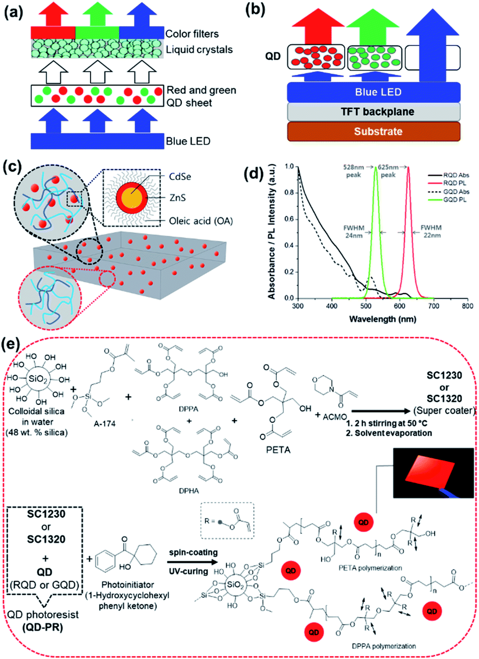 | ||
| Fig. 1 (a) Schematic representation of (a) the commercially available QLED and (b) the QD display developed in this study. (c) Schematic representation of the “QD photoresist (QD-PR)” or “KU-QD-photoresist,” which is the final blend of QDs (zoomed black dotted square) and a super coater (zoomed dotted red circle). The QDs have a core–shell structure of CdSe and ZnS surrounded by an oleic acid ligand. (d) Absorption spectra (solid and dotted black curve) and fluorescence spectra (red and green curve) for red and green QDs, respectively. (e) Materials and protocol for the synthesis of the specially designed super coater. | ||
Because the size of the QD micro-pattern directly affects the resolution of the QD OLED display, the fabrication technology of QD micro-patterns is crucial for next generation displays. Moreover, the dispersion of QDs in a micro-pattern is another key issue to deliver uniform color and stability. Several approaches have been developed to realize QD micro-patterns, including soft lithography, stamping,11,12 inkjet printing,13–15 3D printing,16 and the lift-off process.17 However, all of them are still incompatible with standard semiconductor processes, limiting their applications in mass production.
This study reports QD photolithography using a custom-developed QD photoresist composed of an organic–inorganic hybrid coating layer. There are limited reports on QD photolithography using conventional photolithography processes suitable for mass production. Hence, the proposed study firstly demonstrates the development of the QD photoresist, the QD photolithography process steps, and all the process parameters. We have utilized a basic structure of the color-by-blue approach to develop QD subpixels for display applications.18 The blue sub-pixel is transparent to blue light emission, while the green and red sub-pixels with QDs absorb blue light and convert it to green and red light, respectively (Fig. 1b). Based on all these developments, various QD micropatterns including red or green microlines, RGB color filters for smartphone displays at 340 ppi and atypical Korea University micrologo patterns have been successfully fabricated and demonstrated, highlighting their potential for display, semiconductor and biosensor applications.
Experimental section
Fabrication of the QD photoresist
The QD photoresist used in photolithography was a composite of QDs and a photocurable nano-silica acrylate ceramer. The photocurable ceramer composite developed in this study was named ‘Super Coater’. The final blend of QDs and the super coater was named the 'QD photoresist (QD-PR) ‘or’ KU-QD photoresist'. The red and green QDs were purchased from Dong-A Carbon Tech (Chilgok, Republic of Korea). The QDs had a core–shell structure of CdSe and ZnS wrapped in an oleic acid ligand (Fig. 1c). During exposure, a component of the super coater, the photoactive compound (PAC), produces free electrons in the exposed area, and the acrylate begins to bond and is cured. By contrast, the unexposed area covered by the photomask remains in the solution state (Fig. 1). After exposure, the cured portion remains on the substrate during the development process, while the unexposed part in the solution state is washed off to accomplish selective photocuring, allowing a QD micro-patterning with a sharp FWHM in the green (λpeak = 528 nm) or red (λpeak = 625 nm) color region (Fig. 1d).In this study, we developed two types of super-coaters based on the mixing ratio of silica and acrylate: SC1230 and SC1320, as listed in Table 1.
| Super coater | Components | ||||
|---|---|---|---|---|---|
| DPPA/DPHA (wt%) | PETA (wt%) | Colloidal silica suspension (wt%) | A-174 (wt%) | ACMO (wt%) | |
| SC1230 | 5 | 35 | 48 | 6 | 6 |
| SC1320 | 8 | 56 | 16 | 10 | 10 |
SC1230 was prepared by stirring (for 2 h at 50 °C) and solvent evaporation of the following mixture of 48 wt% colloidal silica suspension in water (Sigma-Aldrich, USA), 6 wt% silane compound 3-(methacryloyloxy) propyltrimethoxysilane (A-174, Alfa Aesar, USA), 5 wt% dipentaerythritol penta-/hexa-acrylate (DPPA/DPHA) (Sigma-Aldrich, USA), 35 wt% pentaerythritol triacrylate (PETA) stabilized with 300–400 ppm 4-methoxyphenol (MEHQ) (Alfa Aesar, USA), and 6 wt% 4-acryloylmorpholine (ACMO) stabilized with MEHQ (Tokyo Chemical Industry, Japan) (Fig. 1e). In a similar manner, SC1320 was fabricated based on the following reagents: 16 wt% colloidal silica, 10 wt% A-174, 8 wt% DPPA/DPHA, 56 wt% PETA, and 10 wt% ACMO. For the UV curing process, 3 wt% photoinitiator (1-hydroxycyclohexyl phenyl ketone, Tokyo Chemical Industry, Japan) was added to each QD-PR mixture which is prepared from mixing of QDs (RQDs or GQDs) and super coater (SC1230 or SC1320). Fig. 1 shows the absorbance and PL spectra of the QDs used for the development of the QD-PR. The absorbance and PL spectra were measured using a Cary 5000 UV-vis-NIR Spectrometer (Agilent Technologies, USA) and Cary Eclipse Fluorescence Spectrophotometer (Agilent Technologies, USA), respectively. The fluorescence intensity of the red QD had a half-width of 22 nm at a peak of 625 nm, and a half-width of 30 nm when mixed with a super coater. The fluorescence intensity of the blue QD had a FWHM of 24 nm at a 528 nm peak and a FWHM of 29 nm when mixed with a super coater. QDs were stored and dispersed in chloroform. QD aggregation occurred when many QDs were introduced into the super coater, causing the FWHM to increase by a small amount.19,20
Optimization of QD photolithography techniques
In this study, the QD-PR was used as a negative photoresist. In the exposed region, the free electrons generated by the photo-initiator bonded with the acrylate, thereby curing the QD-PR. The unexposed mask-covered region remained in the liquid state and was washed away during the development process.In a typical photoresist process, the target substrate was coated with a photoresist by spin coating, followed by soft baking to remove the excess photoresist solvent. After baking, the photoresist film was exposed to ultraviolet light through a photomask to transfer the geometric pattern. The light exposure causes a chemical reaction between the resist and the light. Only those areas unprotected by the mask undergo a chemical reaction, and the mask pattern is transferred to the target substrate during the development process. The procedure using the QD-PR was identical to that described above. A thin film was formed by spin coating on the target substrate. Soft baking was conducted when there was solvent, and development was applied after exposure to complete the QD pattern. An evaporation process applying soft baking was required by including chloroform in the mixture because the purpose was to implement a thin film and the pattern thickness through a process when using the QD-PR with SC1320. On the other hand, all solvents were evaporated during the QD-PR fabrication process because the purpose of the QD-PR using SC1230 was to improve the dispersion of QDs mixed at a high weight ratio. Therefore, the soft baking process during photolithography was omitted for the QD-PR using SC1230.
Fig. S1† presents the spin curves of the QD-PR fabricated using SC1320 and SC1230. Both materials were spin-coated for 120 s, 150 s, and 180 s at 3000 rpm, 4000 rpm, and 5000 rpm, respectively. For the formation of a smooth thin film, the surface was plasma treated before the spin-coating procedure. The thickness of the cured film was measured using a KLA-Tencor Alpha-Step IQ Surface Profilometer. The process was repeated three times under each spin coating condition. Under the same spin coating conditions, the SC1320 film thickness ranged from 1.2 μm to 2.6 μm, whereas the SC1230 film thickness ranged from 5.6 μm to 9.2 μm. The viscosity of the super coater can be controlled by adjusting the acrylate-to-nano silica ratio. SC1320 has a low viscosity, resulting in a thin layer. By contrast, SC1230 has a high viscosity, resulting in a thicker coating. The spin-coating film thicknesses can be modeled using a power-law equation, such as h = Aωn.21 In this expression, h is the thickness of the produced film; ω is the spin speed; A is a constant given by the conditions of the object, such as the structure of the material, the ratio of the solution, and evaporation rate; n is the power-law coefficient.
Fig. S2† shows the double logarithmic representation of the spin curves of SC1320 and SC1230, i.e., both x values (spin speed in rpm) and y values (thickness in nm) are plotted on a logarithmic scale. A linear approximation was used to fit the spin curve data (on a log–log scale). Here, n represents the slope of the linearly fitted curve in Fig. S2,† and was −1.43 at 120 s, −1.39 at 150 s, and −1.46 at 180 s for SC1320, and −0.71 at 120 s, −0.69 at 150 s, and −0.67 at 180 s for SC1230. The slope in the log scale remained constant despite the varying spin coating time for the two different materials.
The degree of dispersion of QDs in the QD film had to be checked first because aggregation of QDs can lead to luminescence quenching of QDs due to increased reabsorption and light scattering, Fig. S3†.22 It was found that the SC1230 film was more uniform than the SC1320 film despite the higher wt% of QDs. Aggregation was observed in SC1320 due to the low weight ratio of colloidal silica, although the QDs were mixed in a low weight ratio.
During the exposure process, an MDS-400S mask aligner (MIDAS, Republic of Korea) was used in conjunction with an Osram 350 W UV lamp as the light source. Furthermore, experiments were performed to optimize the exposure step, which follows the spin coating process. When exposed for 200 s, the pattern transferred most of the photomask, and the sample exposed for 150 s formed a pattern thinner than the photomask. A broad line pattern was formed in the sample exposed for 300 s, and the unexposed part between the patterns was also cured and did not develop, remaining as a defect. Overall, exposure conditions of 200 s at 300 W produced the best results, and these conditions could be fine-tuned by the film thickness.
Experiments with various liquids were performed to choose a developer for the development process. Initially, the QD-PR solution was not washed away when the development process was conducted with DI water, and it remained in the unexposed area. The development process was then carried out using organic solvents, such as chloroform, methyl alcohol, and isopropyl alcohol, with varying results depending on the organic solvent used. Although chloroform effectively removed the uncured QD-PR, the pattern collapsed partly because of the decrease in adhesion between the cured QD pattern and the glass substrate. On the other hand, the pattern in isopropyl alcohol was difficult to distinguish because the QD-PR between the line patterns remained. The use of methanol and acetone during the development process allowed the uncured QD-PR to be washed cleanly, and the line patterns were clearly defined. Among these two solvents, methanol was chosen as a developer because it can conduct a blow-drying process cleanly while simultaneously achieving development and rinsing.
Fabrication processes for the QD color filter
Fig. 2 shows a schematic diagram of the steps involved in the production of a QD color filter. In the first step, a quartz substrate was ion coated with a 100 nm chrome layer. After spin coating a photoresist onto the coated chromium layer, a photomask was then used to define the black matrix pattern. The photoresist (AZ-5214E) was developed by immersing it in an AZ-300 MIF developer solution for 20 s after exposing it to 200 W for 12 s using a mask aligner. The photoresist of the black matrix pattern produced by photolithography was hard-baked at 100 °C for 60 s to serve as the etching mask. The exposed chromium layer was etched by immersing it in a chromium etchant for 25 s and then rinsing it with deionized water. The remaining photoresist after chromium etching was removed with acetone to complete the chromium black matrix layer and the entire pixel pattern. Depending on the optical measurement result, a 10 wt% QD-PR was used to fabricate the red pixel pattern, and the exposure process was conducted after spin coating on a black matrix. The substrate was spin-coated for 90 s at 7000 rpm to achieve a film thickness of 5 μm. After aligning the red pixel photomask, the red QD-PR was exposed for 180 s at 300 W, a condition obtained through the optimization process. The cured QD-PR patterns adhered to the substrate, and the uncured QD-PR was washed away easily with methanol injection. Methanol was used for both development and rinsing, and the remaining solution was blow-dried with nitrogen gas. | ||
| Fig. 2 A diagram depicting the steps involved in the fabrication of QD OLEDs. (a) Production of pixel definition by coating a 100 nm chromium layer and creating a black mask pattern; (b) exposure and development of the photoresist (c) etching of the Cr layer; (d) washing of the photoresist to obtain the pixel pattern; (e) spin-coating the red QD-PR and alignment of the photomask; (f) red pixel obtained after exposure, development and washing process; (g) spin coating and mask alignment of the green QD-PR; (h) green pixel obtained after exposure, development and washing processes. | ||
The method used to express the green pixels was similar to that used to express the red pixels. A 40 wt% QD-PR was used, and a 5 μm thick QD film was obtained by spin coating for 90 s at 7000 rpm. After aligning the green pixel photomask, the green QD-PR was exposed for 150 seconds at 300 W. A QD micro-pattern was obtained after completing the development and rinsing processes with methanol. Blue light illumination was used to form an RGB pixel pattern. The chromium etchant was purchased from Sigma-Aldrich. Acetone (99.5%) and methyl alcohol (99.5%) were purchased from Samchun Pure Chemicals.
Fig. S4† presents a layout of the design using a layout editor called K-layout for the photomask used in the red and green QD process. The four photomask layouts in Fig. S4a† are a black matrix pattern and an RGB pixel pattern for etching a chromium layer, respectively. Although four photomask steps were produced, the photomask for the blue QD was not used because it was not patterned. Each photomask layout was composed of an RGBG pixel pattern (Pentile structure), an RGB pixel pattern (a line structure), a KU symbol, and a normal line width of 1–10 μm. To produce the RGBG pixels, a display image of a Samsung Galaxy S9, shown in Fig. S4b,† was referenced and arranged in a layer suitable for each color after implementation with a layout editor (Fig. S4c†). The red pixel length was 25 μm, the green pixel length was 17 μm, and the blue pixel length was 29 μm. In addition, the dot pitch representing the distance between the adjacent pixels for the same color was 75 μm and achieved 340 ppi. The dot pitch of a Samsung Galaxy S10+ referenced in developing the pixel layout was 48 μm and had a 526 ppi.
Results and discussion
Optical properties of QD films
More QDs can be mixed in the QD-PR owing to the high viscosity of SC1230, allowing optical and electrical measurements at various wt%. The lumens, CIE 1931 color space, and external quantum efficiency (EQE) of the 10 μm QD film fabricated with different QD weight percentages were measured after applying 60 mA. Moreover, EQE(B) denotes the EQE of the blue LED, and EQE(QD) denotes the EQE of the QD film, expressed as| EQE(T) = EQE(B) + EQE(QD) | (1) |
In addition, photoluminescence quantum efficiency PLQE(QD) is expressed as
| EQE(QD)wt%/EQE(B)bare − EQE(B)wt% | (2) |
which is a value with a ratio of EQE(QD) and a reduction of EQE(B) when a QD film from EQE(B) is used with only an LED. A 450 nm LED was used as the light source for all measurements. Fig. S5 and S6† show the optical characteristics of a QD film made with a QD-PR containing 5, 10, 20, and 40 wt% red and green QDs, respectively. For SC1230, EQE(B) was significantly lower, and EQE(QD) was significantly higher than that of SC1320. This may be because of the increased number of QDs absorbing photons from the LEDs inside the film. Furthermore, green QDs had a higher PL intensity than the previous experiment using SC1320. The EQE(B) of the green film showed a higher overall value than the EQE(B) of the red film. The EQE of the green film (QD) showed an overall lower value than that of the red film compared to the EQE(B) and EQE(QD) of the red QD film and the green QD film. As a result, the absorption and PL intensity of the green QDs were lower than those of the red QDs, despite having the same thickness and weight ratio. Because the goal of this study was to use the QD pattern implemented using the QD-PR in the display field, it was necessary to choose a condition suitable for this purpose from the different measurement results. In this study, a 40 wt% green QD-PR, which had the lowest EQE(B) (28.15) and the highest EQE(QD) (11.50), and a 10 wt% red QD-PR, which was closest to the EQE(B) (23.32) and EQE(QD) (16.70) of the green QD-PR, were selected because they emit light with the same intensity at the same thickness by minimizing the difference in intensity PL between the two QD films, and hence will have similar luminance values, see Fig. 3. Furthermore, lm W−1, which is a measure of brightness versus power, showed the highest value for the 10 wt% red and 40 wt% green QD-PR, which was also used as a selection criterion.
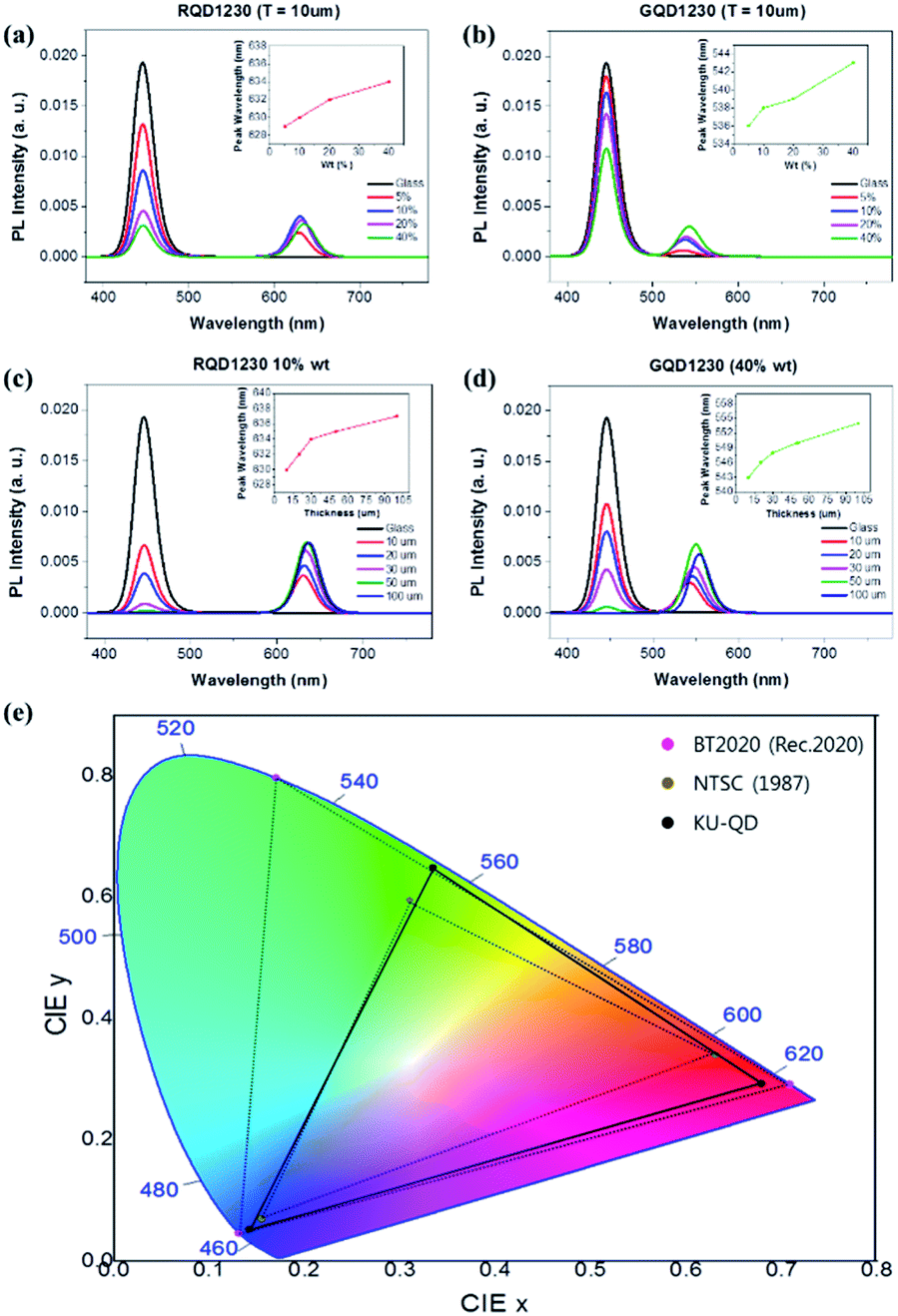 | ||
| Fig. 3 PL spectra of a 10 μm film at various wt% for both red (a) and green QDs (b). The PL spectra of films with thicknesses ranging from 10–100 μm fabricated using the QD-PR containing 10% red QDs (c) and 40% green QDs (d). The PL wavelength peak redshifted in all four cases. (e) Comparison of the NTSC standard and the BT.2020 standard using the CIE 1931 color space implemented in the QD-PR. The CIE 1931 space implemented with KU-QD covered 98.7% of the NTSC (1987) area while providing a more expansive color space. | ||
Fig. S7 and S8† show the optical characteristics of films with thicknesses ranging from 10 to 100 μm fabricated using the QD-PR containing 10% red QDs and 40% green QDs. As the film thicknesses increased, the QDs absorbing blue light increased, and the EQE(B) decreased. For all measurements, the lm W−1 and EQE(QD) values increased with increasing PL intensity. On the other hand, lm W−1 and EQE(QD) were saturated at a 50 μm thickness for both red and green QD-PRs, and the values decreased at 100 μm.
Fig. 3a and b show the PL spectra of the 10 μm film at various wt% for red and green QDs, respectively. Fig. 3c and d show the PL spectra of films with thicknesses ranging from 10–100 μm that were fabricated using the QD-PR containing 10% red QDs and 40% green QDs. The PL wavelength peak redshifted in all four cases with increasing QD weight percent and film thickness. This phenomenon occurred when the QDs inside the film increased, and other QDs reabsorbed the PL light from the adjacent QD.23 The redshift may be due to the reabsorption of PL photons by the adjacent QDs because of the increased number of QDs inside the film. The PL redshift affected the CIE chromaticity that was implemented based on the measurement results of the QD film.
The chromaticity of the QD-PR in the CIE 1931 color space was also compared with those of other standards. Fig. 3e compares the NTSC standard proposed by the National Television System Committee (NTSC) in 1987 and the BT.2020 standard proposed by the International Telecommunication Union (ITU) using the CIE 1931 color space implemented in the QD-PR. The BT.2020 standard covered a wider color space than NTSC, accounting for 76% of the CIE 1931 space. Furthermore, the QDs are gaining popularity in the display industry because the BT.2020 standard can be expressed by a single RGB color of 630, 532, and 467 nm. The CIE 1931 space implemented with the QD-PR covered 98.7% of the NTSC (1987) area while providing a more expansive color space. On the other hand, only 64.5% of the BT.2020 area was covered because the green wavelength of the QD-PR was redshifted to 554 nm. Although this study fell short of the BT.2020 standard, the standard should be met if the QD-PR is fabricated using QDs that emit shorter-wavelength light, considering the redshift of the green QDs.
QD micropatterns using photolithography
The SC1320 film is unsuitable for applications in various fields because the optical and electrical properties of the QD film fabricated with SC1320 were inferior to those of SC1230. To compensate for this, the wt% of the QDs mixed in the QD-PR was increased after re-examining the characteristics by fabricating a QD film with SC1230, securing better optical and electrical characteristics. After ensuring the applicability, photolithography was performed with the QD-PR generated using SC1230, and the outcome is shown in Fig. 4.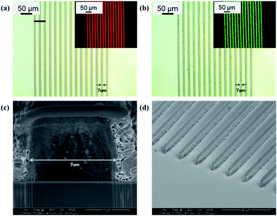 | ||
| Fig. 4 Optical and fluorescence microscopy images (inset) of 7 μm line patterns of red (a) and green (b) QDs, respectively. Cross-sectional (c) and birds-eye view (d). SEM images of the photolithographic line pattern shown in (a) and (b). | ||
Fig. 4a and b present the optical and fluorescence microscopy images of 7 μm line patterns of red and green QDs, respectively, fabricated by photolithography. The measurements were conducted on a plasma surface-treated glass substrate for smooth film formation using spin coating. It was difficult to generate a line pattern with a width less than 7 μm because it was impossible to obtain a film thinner than 5 μm because of the high viscosity of the QD-PR as all solvents evaporated during the QD-PR manufacturing process. Fig. 4c and d show the SEM images of the QD pattern. The samples were coated with a thin layer of Pt before SEM imaging. Section milling and imaging were conducted using a Helios Nanolab Dual Beam FIB system (FEI, Thermo Fisher Scientific Inc.)
Based on these findings, a proof-of-concept display with the QD pixel pattern was produced to illustrate the application of the QD-PR in the display field. Fig. 5a shows the optical images of a pentile structured RGBG pixel pattern containing red and green QDs at 100× and 200× magnification. The red and green QD patterns were fabricated on a black matrix produced using a chromium layer, and a 365 nm LED light source was used for back illumination. The fluorescent red and green lights were emitted from the red and green subpixels fabricated with the QD-PR, and 365 nm LED light was transmitted through the blue subpixels that were empty at the rear, finally obtaining the three RGB hues. The size of each pattern was 25 μm for red, 17 μm for green, and 29 μm for blue, with 340 ppi and a dot pitch of 75 μm. A square-structured RGB pixel pattern was also developed, see Fig. 5b. This square pixel was 95 μm wide, and 112 μm long, with each subpixel made up of three 8 μm lines to achieve a density of 220 ppi and a dot pitch of 112 μm. The image was taken after irradiating with a 365 nm LED light source in an optical microscope similar to that of the pentile structure. This pixel size is well suited for applications in a 40-inch 8 K (7680 × 4320) display.
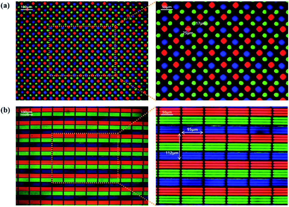 | ||
| Fig. 5 (a) Optical images of the pentile-structured RGBG pixel pattern containing red and green QDs at 100× and 200× magnification (inset). A 365 nm LED light source was used for back illumination, and red and green QD patterns were produced on a black Cr matrix layer. The 365 nm LED light was delivered through the vacant blue pixels at the back to provide the three RGB hues. With 340 ppi and a 75 μm dot pitch, each design was 25 μm (red), 17 μm (green), and 29 μm (blue) in size. (b) The optical images of the square-structured RGB pixel pattern at 100× and 200× magnification (inset). This square pixel was 95 μm wide and 112 μm long, with each subpixel made up of three 8 μm lines. | ||
Finally, a Korea University logo was fabricated using the QD-PR. The logo was imaged in the same way as the pixel pattern, and the width and length of the entire pattern were 440 and 660 μm, respectively, as shown in Fig. 6. Although the minimum line width implemented using photolithography was specified above as 7 μm, the minimum line width for the KU logo implemented using the QD-PR was 4–5 μm (insets of Fig. 6). This is because the pattern of the chromium layer was at the forefront relative to the microscope lens. Moreover, the QD pattern on the backside was covered with a chromium pattern even though it was larger. A pattern with a smaller size can also be implemented by taking advantage of the fact that the QD pattern size can be defined by the pattern size of the chromium layer.
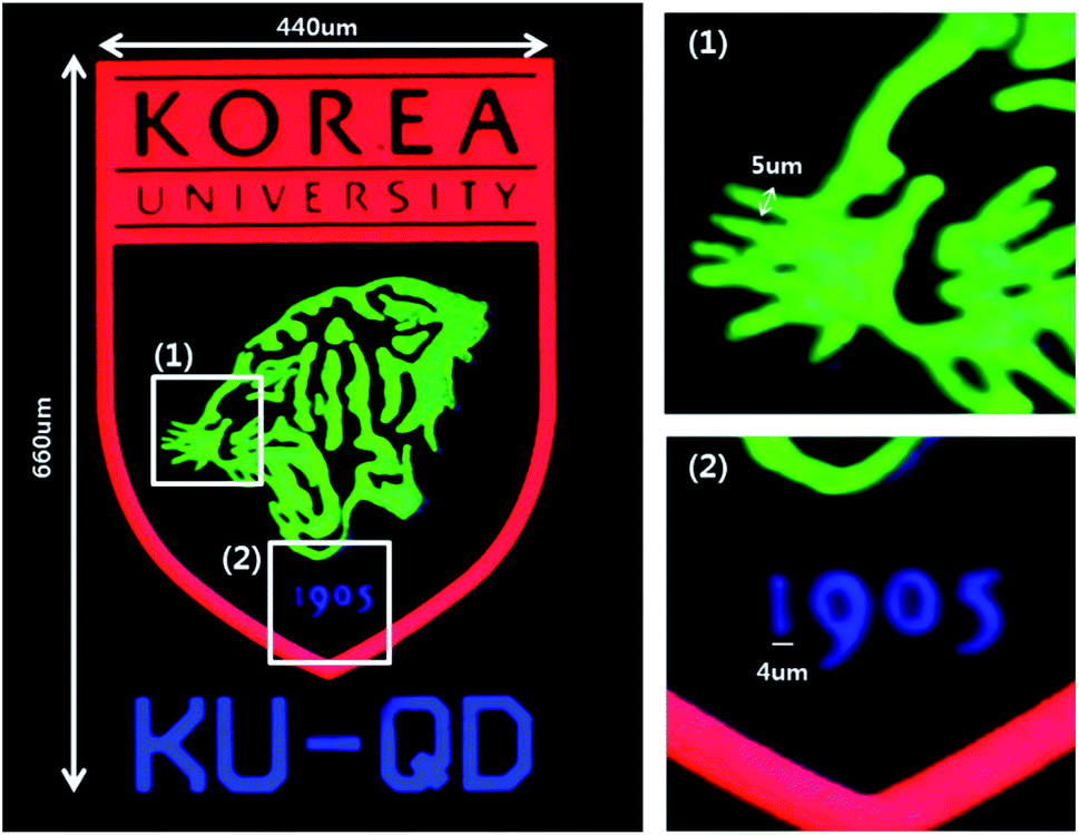 | ||
| Fig. 6 Korea University logo fabricated using the QD-PR. For the KU logo, the minimum line width accomplished using the QD-PR was 4–5 μm. | ||
Conclusions
This paper reports a QD-PR by combining QDs in the super coater to produce patterns on a micrometer scale through photolithography for applications in next-generation displays. The super coater is a custom-developed photocurable nano-silica-acrylate ceramer synthesized by Korea University. An RGBG small display pixel pattern of 340 ppi and an RGB large display pixel pattern of 220 ppi were realized using this QD-PR. Furthermore, its application to next-generation displays was demonstrated by comparing the color coordinates of the QD film with those of the BT.2020 standard. On the other hand, there are still tasks to be solved through further research before the results of this study can have actual applications. The blue BLU needs to be color converted completely into red or green even in a thin film state, such as the pixel pattern for complete application to a QD display device. As a result of the experiment described in this paper, a red QD-PR emitted a clear intact red light under a 50 μm thickness at 10 wt%, and a green QD-PR also emitted a clear green light under the same thickness at 40 wt%. The results are expected to find applications in QD display technology if the wt% of the QDs and the process can be optimized to reduce this thickness. In addition, the scope of this study was more of a demonstration close to the technology of QD displays by exciting the samples of the completed pixel pattern using 365 nm LEDs. The final goal of this study can be reached, but further research on implementing a complete QD display by demonstrating it on a blue BLU and reducing the color conversion thickness will be needed. Furthermore, a high-resolution display of 800 ppi or higher may be developed by applying a QD pattern of at least 7 μm. This allows QDs to be applied from a 4 K small display (3840 × 2160 pixels, 6.1 inches) to a larger display with a resolution greater than 16 K (15![[thin space (1/6-em)]](https://www.rsc.org/images/entities/char_2009.gif) 360 × 8640 pixels, 24 inches). Although the technique presented in this study was limited to next-generation displays, the photolithography implementing a QD micro-pattern is expected to be applied in a wide variety of QD-based technologies, such as bio-labeling, optical detectors, and solar cells.
360 × 8640 pixels, 24 inches). Although the technique presented in this study was limited to next-generation displays, the photolithography implementing a QD micro-pattern is expected to be applied in a wide variety of QD-based technologies, such as bio-labeling, optical detectors, and solar cells.
Author contributions
Conceptualization, S. O. K., S. S.; methodology, S. M., B. C.; validation, S. M., B. C., H. S.; writing – original draft preparation, S. M., S. S.; writing – review and editing, H. S., S. K., S. S.; supervision, S. O. K., S. S.; project administration, S. O. K., S. S.; funding acquisition, S. O. K., S. S.Conflicts of interest
There are no conflicts to declare.Acknowledgements
This study was supported by the Basic Science Research Program (Grant No. 2014R1A6A1030732, Grant No. 2020R1A2C1012109) through the National Research Foundation (NRF) of Korea. This work was supported by the Korea Medical Device Development Fund grant funded by the Korean Government (the Ministry of Science and ICT, the Ministry of Trade, Industry and Energy, the Ministry of Health & Welfare, the Ministry of Food and Drug Safety) (Project No. 202012E04) and a part of the projects titled ‘Development of Management Technology for HNS Accident’ and ‘Development of Technology for Impact Assessment and Management of HNS discharged from Marine Industrial Facilities’, funded by the Ministry of Oceans and Fisheries, Republic of Korea.Notes and references
- V. Esch, B. Fluegel, G. Khitrova, H. M. Gibbs, J. Xu, K. Kang, S. W. Koch, L. C. Liu, S. H. Risbud and N. Peyghambarian, Phys. Rev. B: Condens. Matter, 1990, 42, 7450–7453 CrossRef CAS PubMed.
- B. Jai Kumar, D. Sumanth Kumar and H. M. Mahesh, J. Lumin., 2016, 178, 362–367 CrossRef CAS.
- L. E. Brus, J. Chem. Phys., 1984, 80, 4403–4409 CrossRef CAS.
- M. T. Nenadovic, T. Rajh and O. I. Micic, J. Phys. Chem., 1985, 89, 397–399 CrossRef CAS.
- Z. Lingley, S. Lu and A. Madhukar, Nano Lett., 2011, 11, 2887–2891 CrossRef CAS PubMed.
- F. Dubois, B. Mahler, B. Dubertret, E. Doris and C. Mioskowski, J. Am. Chem. Soc., 2007, 129, 482–483 CrossRef CAS PubMed.
- A. Ruland, C. Schulz-Drost, V. Sgobba and D. M. Guldi, Adv. Mater., 2011, 23, 4573–4577 CrossRef CAS PubMed.
- H. Wang, L. Sun, Y. Li, X. Fei, M. Sun, C. Zhang, Y. Li and Q. Yang, Langmuir, 2011, 27, 11609–11615 CrossRef CAS PubMed.
- W. R. Algar, A. J. Tavares and U. J. Krull, Anal. Chim. Acta, 2010, 673, 1–25 CrossRef CAS PubMed.
- E. Hsiang, Z. Yang, Q. Yang, Y. Lan and S. Wu, J. Soc. Inf. Disp., 2021, 29, 446–465 CrossRef.
- M. K. Choi, J. Yang, K. Kang, D. C. Kim, C. Choi, C. Park, S. J. Kim, S. I. Chae, T.-H. Kim, J. H. Kim, T. Hyeon and D.-H. Kim, Nat. Commun., 2015, 6, 7149 CrossRef CAS PubMed.
- H. Keum, Y. Jiang, J. K. Park, J. C. Flanagan, M. Shim and S. Kim, ACS Nano, 2018, 12, 10024–10031 CrossRef CAS PubMed.
- H. M. Haverinen, R. A. Myllyla and G. E. Jabbour, J. Disp. Technol., 2010, 6, 87–89 CAS.
- J. Han, D. Ko, M. Park, J. Roh, H. Jung, Y. Lee, Y. Kwon, J. Sohn, W. K. Bae, B. D. Chin and C. Lee, J. Soc. Inf. Disp., 2016, 24, 545–551 CrossRef CAS.
- C. Jiang, Z. Zhong, B. Liu, Z. He, J. Zou, L. Wang, J. Wang, J. Peng and Y. Cao, ACS Appl. Mater. Interfaces, 2016, 8, 26162–26168 CrossRef CAS PubMed.
- Y. L. Kong, I. A. Tamargo, H. Kim, B. N. Johnson, M. K. Gupta, T.-W. Koh, H.-A. Chin, D. A. Steingart, B. P. Rand and M. C. McAlpine, Nano Lett., 2014, 14, 7017–7023 CrossRef CAS PubMed.
- J.-S. Park, J. Kyhm, H. H. Kim, S. Jeong, J. Kang, S.-E. Lee, K.-T. Lee, K. Park, N. Barange, J. Han, J. D. Song, W. K. Choi and I. K. Han, Nano Lett., 2016, 16, 6946–6953 CrossRef CAS PubMed.
- J. H. Oh, K.-H. Lee, H. C. Yoon, H. Yang and Y. R. Do, Opt. Express, 2014, 22(2), A511–A520 CrossRef PubMed.
- S. Mandal, A. Gole, N. Lala, R. Gonnade, V. Ganvir and M. Sastry, Langmuir, 2001, 17, 6262–6268 CrossRef CAS.
- J. Liu, X. Yang, K. Wang, X. He, Q. Wang, J. Huang and Y. Liu, ACS Nano, 2012, 6, 4973–4983 CrossRef CAS PubMed.
- J. P. H. Lima and A. M. de Andrade, J. Mater. Sci.: Mater. Electron., 2006, 17, 593–596 CrossRef CAS.
- J. Liu, X. Yang, K. Wang, R. Yang, H. Ji, L. Yang and C. Wu, Chem. Commun., 2011, 47, 935–937 RSC.
- W. Zhang, D. Dai, X. Chen, X. Guo and J. Fan, Appl. Phys. Lett., 2014, 104, 091902 CrossRef.
Footnotes |
| † Electronic supplementary information (ESI) available. See DOI: 10.1039/d1na00744k |
| ‡ These authors contributed equally |
| This journal is © The Royal Society of Chemistry 2022 |