
 Open Access Article
 This Open Access Article is licensed under a Creative Commons Attribution-Non Commercial 3.0 Unported Licence
Polarization-insensitive broadband omni-directional anti-reflection in ZnO nanoneedle array for efficient solar energy harvesting†
Minjee
Ko
a,
Hyeon-Seo
Choi
a,
Seong-Ho
Baek
*b and
Chang-Hee
Cho
 *a
*a
aDepartment of Emerging Materials Science, Daegu Gyeongbuk Institute of Science and Technology (DGIST), Daegu 42988, South Korea. E-mail: chcho@dgist.ac.kr
bDepartment of Energy Engineering, Dankook University, Cheonan 31116, South Korea. E-mail: seongho@dankook.ac.kr
First published on 14th January 2022
Abstract
Broadband omni-directional anti-reflection characteristics have been an important issue because they can maximize the optical absorption in photovoltaic devices. Here, we investigate the optical properties of ZnO nanoneedle arrays to demonstrate broadband anti-reflection, omni-directionality, and polarization insensitivity using optical simulations and experimental approaches. The results of this work clarify that the ZnO nanoneedle array plays an important role as a broadband anti-reflection layer due to its spatially graded refractive index, omni-directionality and polarization insensitivity. To take advantage of these structures, we prepared a ZnO nanoneedle array on the surface of conventional SiNx/planar Si solar cells to prove the broadband omni-directional anti-reflection for solar energy harvesting. Current density–voltage results show that SiNx/planar Si solar cells with ZnO nanoneedle arrays lead to a nearly 20% increase in power conversion efficiency compared to SiNx/planar Si solar cells, and a 9.3% enhancement in external quantum efficiency is obtained under identical conditions. Moreover, the photocurrent results of SiNx/planar Si solar cells with ZnO nanoneedle arrays clearly demonstrate the incident angle- and polarization-insensitive characteristics compared to those of typical SiNx/planar Si solar cells. Our results demonstrate the optical multi-functionality of ZnO nanoneedle arrays and pave the way for high-performance optoelectronic devices that require broadband omni-directional anti-reflection and polarization insensitivity.
Introduction
To obtain high-efficiency light absorption in optoelectronic devices such as solar cells and photodetectors, the minimized reflection by introducing intermediate refractive index materials at the boundary between air and light absorbers is of great importance. Generally, quarter-wavelength anti-reflection (AR) coating with silicon nitride (SiNx) film is widely used to suppress optical reflection in Si-based photovoltaic devices.1,2 However, the disadvantage of SiNx AR coatings lies in their ability to reduce the light reflection only in a narrow range of wavelengths and incident angles,3,4 which restricts the use of SiNx films for broadband AR effects. Therefore, they are not suitable for photovoltaic device applications that target spectral broadband and off-normal incident light absorption.To address these problems, the proposed approaches include the multilayer thin films consisting of various refractive indices,5,6 the designed dielectric micro-/nano-structures that induce a graded refractive index,7–15 and the optical resonance structures for efficient light confinement.16–22 Furthermore, metamaterials, which do not exist in nature, can directly control the optical constants of permittivity, permeability, refractive index, and impedance and facilitate extreme optical properties such as perfect absorption, reflection, and transmission.23–25 Using this approach, broadband light absorption, omni-directional properties, and polarization insensitivity can be achieved to realize highly efficient optical absorbers. However, the preparation of metamaterials requires very complex fabrication processes, which suffer from difficulties in practical applications. On the other hand, the monolithically formed micro-/nano-structures26,27 on light absorbing materials often increase surface recombination channels, which deteriorate the power conversion efficiency due to the undesired surface damages.28–30 Thus, to suppress the degradation in electrical performances, additional semiconductor fabrication processes such as an passivation layer deposition or doping concentration control are required.31–34 Therefore, it is highly desirable to investigate multi-functional nanostructures that enable polarization-insensitive broadband omni-directional AR properties, which can readily be applied to conventional photovoltaic devices without compromising the power conversion efficiency. Until now, there have been various AR approaches that provide optical benefits, but few studies have applied them to conventional solar cell devices.
In this work, we investigated the optical properties of ZnO nanoneedle (NN) arrays for the use of broadband omni-directional AR coating. First, using the finite-difference time-domain (FDTD) method, the reflection and transmission spectra of the ZnO NN array were simulated as a function of the incident angle, and we found that the ZnO NN array exhibited broadband omni-directional AR characteristics. To verify the effects of the ZnO NN array on photovoltaic device characteristics, Si p–n junction solar cells with the ZnO NN array were prepared and characterized in comparison to conventional SiNx AR-coated solar cells. They showed greatly improved characteristics of broadband omni-directional AR and angle- and polarization-insensitive properties for Si solar cells with ZnO NN arrays. Our results suggest that the ZnO NN array can be used for the broadband omni-directional and polarization-insensitive AR coating layer, which can be easily applied to various optoelectronic devices.
Results and discussion
Using FDTD simulations, we investigated the optical properties of ZnO NN arrays over a broadband wavelength range for varying incident angles. Details of the FDTD simulations can be found in the numerical simulation section and Fig. S1 of ESI.† The optical constant of ZnO material used in the simulations is shown in Fig. S2.† In order to investigate the geometric effect on the reflection and transmission through ZnO NN array, we have carried out the comparative study with varying the structural parameters such as the diameter and height (Fig. S3 and S4†). Based on the simulation results, we have designed the ZnO NN array with a height of 230 nm, a diameter of 50 nm, and a period of 50 nm, as shown in Fig. 1(a). Fig. 1(b) and (c) present the calculated reflection and transmission spectral maps, respectively, for the ZnO NN array over the wavelength range of 400–800 nm as a function of the incident angle (θ) of 0–64°. The results exhibit near-zero reflection and near-unity transmission which appear as single colors in the maps. These indicate broadband AR and transmission characteristics, which are insensitive to the incident angle. Notably, a weak reflection (∼8%) in the wavelengths of 500–700 nm is observed at nearly normal incidence angles (θ < 10°), and the reflection gradually decreases with increasing incident angle, which forms near-zero reflection. Thus, the ZnO NN array retains the excellent broadband AR with omni-directionality for off-normal incidence conditions. The significantly reduced broadband reflection with omni-directionality can be ascribed to the impedance matching effect at the optical interfaces.9 Due to the graded-index geometry from top to bottom of the ZnO NN structure, it does not obey the general Fresnel reflection, which can be applied to the interfaces with an abrupt change in refractive index experienced by incident light. The gradual impedance matching between air and ZnO NN arrays significantly reduces the reflection at the surface of ZnO NN arrays.35,36 The observed omni-directionality occurs because the light–matter interaction is governed by scattering processes between ZnO NNs and incident light, which are less sensitive to the angle of incidence. These effects also lead to near-unity transmission through the ZnO NN array over a broad wavelength range for wide incident angles (Fig. 1(c)). Meanwhile, the rescaled color maps of Fig. 1(b) and (c) are presented in Fig. S5† to maximize the visibility of the results.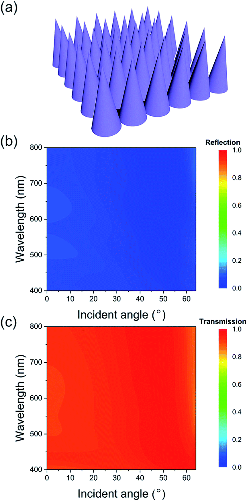 | ||
| Fig. 1 Simulated optical properties of ZnO nanoneedle array. (a) Schematic image of the designed ZnO nanoneedle array with a height of 230 nm, diameter of 50 nm, and period of 50 nm for FDTD simulation. (b and c) Angle-resolved reflection (b) and transmission (c) spectral map as a function of the wavelength for the ZnO nanoneedle array. | ||
To experimentally demonstrate the simulated optical characteristics, a ZnO NN array was grown on 100 nm-thick SiNx/planar Si using a hydrothermal method, as shown in Fig. 2(a) and (b). We also prepared a 100 nm-thick SiNx film on a planar Si substrate as a control sample. The detailed fabrication method is described in ESI.† The structural parameters, such as the height and diameter, for the grown ZnO NN array are consistent with those in the numerical calculations, although the ZnO NNs are arranged nonperiodically in the experiments. The magnified SEM image of ZnO NNs exhibits the tapered shape (Fig. S6†), resulting in a graded-refractive index profile that enables reduced reflection due to the enhanced impedance matching. Fig. 2(c) shows the measured diffuse reflectance spectra for the samples using a spectrophotometer with an integrating sphere. The results indicate that the SiNx/planar Si without the ZnO NN array shows reduced reflectance only at specific wavelengths of approximately 800 nm. It is a typical single-layer AR characteristic that works only at a single wavelength, λ ∼ 4nd, where λ is the wavelength, n is the refractive index, and d is the film thickness. This layer creates out-of-phase reflected waves that are related to the thickness of SiNx, which causes destructive interference for the reflected light, reduced reflection and enhanced transmission at a specific wavelength.12 In contrast, the SiNx/planar Si with the ZnO NN array exhibits remarkably lower reflection over a broad range of wavelengths due to the gradual change in refractive index of the ZnO NN array, which results in impedance matching from air through the ZnO NN array to the SiNx layer and produces broadband AR characteristics, which is also confirmed in FDTD calculations (Fig. S7†). The observed interference fringes in the reflectance spectra of the ZnO NN array on SiNx/planar Si may originate from the Fabry–Pérot oscillation of the reflectance. However, the slightly higher reflectance is observed in the ZnO NN array at the wavelengths of ∼800 nm, at which the AR effect of single-layer SiNx becomes maximized. The strong light absorption below the wavelength of 380 nm is also observed in the SiNx/planar Si with ZnO NN array due to the band edge absorption in ZnO (bandgap: 3.37 eV).37 By integrating the diffuse reflectance in the spectral range from 380 to 800 nm, the integrated value of the SiNx/planar Si with ZnO NN array decreased by ∼68.8% compared to that of bulk planar Si, whereas the SiNx/planar Si without ZnO NN array decreased by ∼44.1%. These results suggest that the ZnO NN array formed on the conventional SiNx AR layer can provide a synergistic effect and exhibits excellent light absorption over broadband wavelengths.
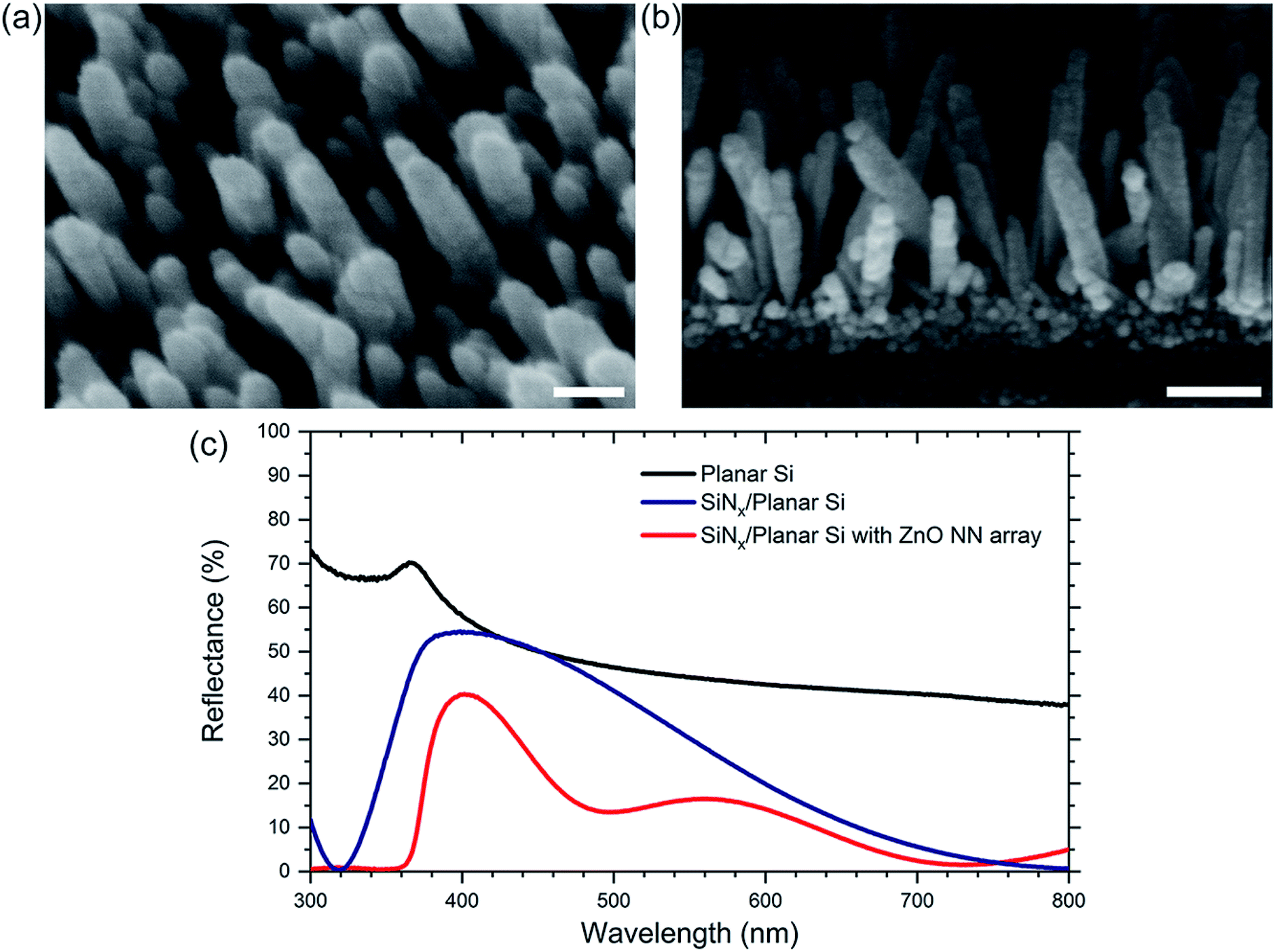 | ||
| Fig. 2 (a and b) Tilted top-view (a) and cross-sectional view (b) SEM images of the fabricated ZnO nanoneedle array grown on SiNx/planar Si substrate. The scale bars of (a) and (b) indicate 50 nm and 100 nm, respectively. (c) Experimental reflectance spectra of the SiNx/planar Si with and without ZnO nanoneedle array. The reflectance spectrum of bare planar Si is also provided for a comparison. | ||
To verify the omni-directional and broadband AR effect of the ZnO NN array, we fabricated SiNx/planar Si solar cells with and without the ZnO NN array based on the p–n junction. Fig. 3(a) and (b) display schematic and real images of the prepared Si solar cells, respectively. The incident angle-resolved photocurrent was measured to investigate the angle-dependent characteristics of the solar cells using a conventional probe station with a source meter (2636B, Keithley). A compact laser diode module at a wavelength of 450 nm was used as a light source, and the laser power density was maintained at 49.6 mW cm−2. Moreover, photocurrent measurements were performed for the TE- and TM-polarization directions as a function of the incident angle from 0 to 70° with 5° increments, as shown in Fig. 3(c) and (d). The inset of Fig. 3(d) indicates the schematic image, showing the definition of TE- and TM-polarizations. The TE-polarized light is characterized by the electric field vector perpendicular to the plane of incidence, while being parallel for the TM-polarized light. As expected, the SiNx/planar Si solar cells with ZnO NN array show greatly enhanced photocurrents over a wide range of incident angles compared to the solar cells without ZnO NN array. For the SiNx/planar Si solar cells without ZnO NN array, the measured photocurrents show a typical angle-dependent behavior, which implies that they obey the Fresnel reflection for the TE and TM-polarizations (The details for Fresnel reflection are explained in the Section 5 of ESI†). For TM-polarization, as shown in Fig. 3(d), the increase in photocurrent at high angles can be understood as the result of Brewster angle effect.38 Fig. S8† exhibits the calculated Fresnel reflection at the interface between air (n = 1) and SiNx (n = 2.07) for TE and TM polarizations along with that of unpolarized light for the incident angle range of 0 to 70°.38 The calculated reflection results are consistent with the measured angle-dependent photocurrents of the SiNx/planar Si solar cells without ZnO NN array for TE- and TM-polarizations. As shown in Fig. 3(c) and (d), the SiNx/planar Si solar cells with ZnO NN array show the excellent polarization insensitivity and omni-directionality over a wide range of incident angles compared to the SiNx/planar Si solar cells without ZnO NN array. Interestingly, the ZnO NN array causes relatively constant photocurrents even at the high angle range around a Brewster angle of ∼64° due to the insensitivity to the angle of incidence. This result can be explained by the inverse polarization phenomenon at the Brewster angle, which arises from the randomization of various directional reflected waves by subwavelength scale nanostructures,39 which is also consistent with the simulation results of angle-dependent reflection and transmission, as provided in Fig. 1. Our results clearly indicate that the ZnO NN array suppresses the Fresnel reflection at the surface between air and the ZnO NN array with the omni-directionality and polarization insensitivity over a broad wavelength range. Solar cells integrated with the ZnO NN array can provide stable performance during sunset and rising times without solar tracking systems.
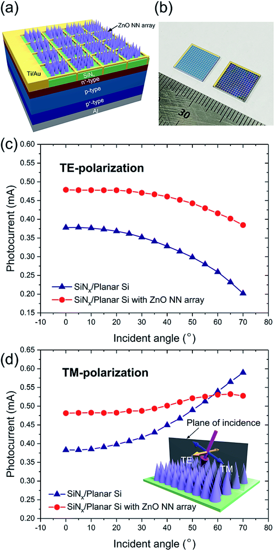 | ||
| Fig. 3 (a and b) Schematic illustration (a) and device image (b) of the Si p–n junction solar cells without (left) and with (right) ZnO nanoneedle array. The gradation of the ruler indicates 1 mm. (c and d) Photocurrents at 0 V as a function of the incident angle under TE- (c) and TM-polarization (d) conditions. The inset shows the measurement set-up for angle-resolved photocurrents. The orange and blue arrows indicate the E-field vector for TE- and TM-polarizations, respectively. The magenta arrow indicates propagating direction with a specific incident angle. | ||
Finally, to confirm the photovoltaic characteristics of the solar cells with a ZnO NN array, we measured the power conversion efficiency under 1 sun illumination (AM 1.5 G, 100 mW cm−2) using a solar simulator (Fig. 4). The photovoltaic parameters of solar cells are summarized in Fig. 4(a) as an inset. Compared to the SiNx/planar Si solar cells, the solar cells with the ZnO NN array show a higher power conversion efficiency of 11.08%, which is enhanced by 19.3% compared with that of the SiNx/planar Si solar cells. From the current density–voltage (J–V) curves in Fig. 4(a), we suggest that the enhanced efficiency is attributed to the increase in short-circuit current (Jsc) due to the broadband AR effect of the ZnO NN array. Additionally, the ZnO NN array Si solar cells exhibit no degradation issues of open-circuit voltage (Voc) because it is electrically insulated from the light-absorbing Si region that generates the photocurrent.28–30,40–42 This result clearly indicates that the ZnO NN array increases the number of photons absorbed into Si due to the reduced reflection at the surface, which contributes to the improved power conversion efficiency. To confirm the enhancement in spectral power conversion efficiency for the ZnO NN array Si solar cells, we measured the external quantum efficiency (EQE) for the fabricated solar cells. As shown in Fig. 4(b), we present the EQE spectra of the SiNx/planar Si solar cells with and without the ZnO NN array. The solar cells with the ZnO NN array exhibit the increased EQE values over the broadband wavelength range, which can be attributed to the strong AR effect of ZnO NN array and the enhanced light absorption in Si. However, in the spectral range of 730–880 nm, the EQE of the solar cells with ZnO NN array is slightly lower than that of the solar cells without ZnO NN array, at which the AR effect of SiNx layer becomes maximized. Over the spectral range from 380 to 1200 nm, the EQE of the solar cells with ZnO NN array is quantitatively increased by ∼9.3%, compared to that of the solar cells without ZnO NN array. In addition, the solar cells with ZnO NN array exhibit an enhancement of EQE by ∼30% at a wavelength of 450 nm, cross-checking the observation of the increased photocurrent results, as shown in Fig. 3(c) and (d). As a result, the ZnO NN array evidently enables the enhancement of the EQE of solar cells over a broad spectral range due to the polarization-insensitive broadband omni-directional AR effect.
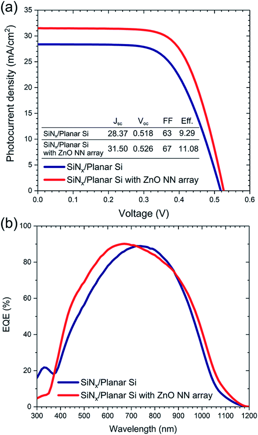 | ||
| Fig. 4 (a) Photocurrent density as a function of bias voltage under illumination (AM 1.5 G) of the solar cells. The measured parameters are presented as a table in the figure. (b) External quantum efficiency spectra of the solar cells with and without the ZnO nanoneedle array. | ||
Conclusions
In summary, we have presented the designed structure of a ZnO NN array on SiNx/planar Si to demonstrate the polarization-insensitive broadband AR and omni-directionality for solar energy harvesting. The simulated and experimental results clearly indicate that the ZnO NN array exhibits broadband AR due to the unique geometry with a graded refractive index, which also enables the polarization-insensitive omni-directional light absorption characteristics. By applying this structure to Si solar cells, we observed that the ZnO NN array enhanced the EQE of solar cells by more than ∼9.3%, compared to the conventional SiNx AR layer due to the polarization-insensitive broadband omni-directional AR effect. Our proposed structure of ZnO NN array, which can be readily applied to conventional solar cells without compromising the efficiency induced by increased surface recombination, can be beneficial for Si-based photovoltaic devices requiring polarization-insensitive omni-directional light absorption.Conflicts of interest
There are no conflicts to declare.Acknowledgements
This work was supported by the Basic Science Research Program (2019R1A2C1088525 and 2020R1C1C1005100) through the National Research Foundation of Korea, and by the DGIST R&D Program (21-CoE-NT-01 and 21-HRHR+-03) funded by the Ministry of Science and ICT of the Korean Government.References
- J. Zhao and M. A. Green, IEEE Trans. Electron Devices, 1991, 38, 1925–1934 CrossRef CAS.
- A. G. Aberle, Sol. Energy Mater. Sol. Cells, 2001, 65, 239–248 CrossRef CAS.
- J. Zhao, A. Wang, P. Altermatt and M. A. Green, Appl. Phys. Lett., 1995, 66, 3636 CrossRef CAS.
- H. Nagel, A. G. Aberle and R. Hezel, Prog. Photovolt.: Res. Appl., 1999, 7, 245–260 CrossRef CAS.
- S. Chhajed, M. F. Schubert, J. K. Kim and E. F. Schubert, Appl. Phys. Lett., 2008, 93, 251108 CrossRef.
- J. F. Lelièvre, B. Kafle, P. Saint-Cast, P. Brunet, R. Magnan, E. Hernandez, S. Pouliquen and F. Massines, Prog. Photovolt., 2019, 27, 1007–1019 CrossRef.
- S. L. Diedenhofen, G. Vecchi, R. E. Algra, A. Hartsuiker, O. L. Muskens, G. Immink, E. P. A. M. Bakkers, W. L. Vos and J. G. Rivas, Adv. Mater., 2009, 21, 973–978 CrossRef CAS.
- A. Rahman, A. Ashraf, H. Xin, X. Tong, P. Sutter, M. D. Eisaman and C. T. Black, Nat. Commun., 2015, 6, 5963 CrossRef CAS PubMed.
- J. Zhu, Z. Yu, G. F. Burkhard, C. M. Hsu, S. T. Conner, Y. Xu, Q. Wang, M. McGehee, S. Fan and Y. Cui, Nano Lett., 2009, 9, 279–282 CrossRef CAS PubMed.
- J. W. Leem, Y. M. Song and J. S. Yu, Nanoscale, 2013, 5, 10455–10460 RSC.
- J. Cai and L. Qi, Mater. Horiz., 2015, 2, 37–53 RSC.
- H. K. Raut, V. A. Ganesh, A. S. Nair and S. Ramakrishna, Energy Environ. Sci., 2011, 4, 3779–3804 RSC.
- N. Kim, D. Choi, H. Kim, H. D. Um and K. Seo, ACS Nano, 2021, 15, 14756–14765 CrossRef CAS PubMed.
- Y. J. Lee, D. S. Ruby, D. W. Peters, B. B. McKenzie and J. W. P. Hsu, Nano Lett., 2008, 8, 1501–1505 CrossRef CAS PubMed.
- L. K. Yeh, W. C. Tian, K. Y. Lai and J. H. He, Sci. Rep., 2016, 6, 39134 CrossRef CAS PubMed.
- M. Ko, S. H. Baek, B. Song, J. W. Kang, S. A. Kim and C. H. Cho, Adv. Mater., 2016, 28, 2504–2510 CrossRef CAS PubMed.
- P. Spinelli, M. A. Verschuuren and A. Polman, Nat. Commun., 2012, 3, 692 CrossRef CAS PubMed.
- Z. Y. Wang, R. J. Zhang, S. Y. Wang, M. Lu, X. Chen, Y. X. Zheng, L. Y. Chen, Z. Ye, C. Z. Wang and K. M. Ho, Sci. Rep., 2015, 5, 7810 CrossRef CAS PubMed.
- A. Prajapati, J. Llobet, P. C. Sousa, H. Fonseca, C. Calaza and G. Shalev, Sol. RRL, 2021, 2100548 CrossRef CAS.
- A. Prajapati, J. Llobet, M. Antunes, S. Martins, H. Fonseca, C. Calaza, J. Gaspar and G. Shalev, Nano Energy, 2020, 70, 104553 CrossRef CAS.
- S. Behera, P. W. Fry, H. Francis, C. Y. Jin and M. Hopkinson, Sci. Rep., 2020, 10, 6269 CrossRef CAS PubMed.
- C. Fang, Z. Yang, J. Zhang, Y. Zhuang, S. Liu, X. He and Y. Zhang, Sol. Energy Mater. Sol. Cells, 2020, 206, 110305 CrossRef CAS.
- R. Maas, J. Parsons, N. Engheta and A. Polman, Nat. Photonics, 2013, 7, 907–912 CrossRef CAS.
- P. Moitra, Y. Yang, Z. Anderson, I. I. Kravchenko, D. P. Briggs and J. Valentine, Nat. Photonics, 2013, 7, 791–795 CrossRef CAS.
- K. Im, J. H. Kang and Q. H. Park, Nat. Photonics, 2018, 12, 143–149 CrossRef CAS.
- H. A. Chaliyawala, Z. Purohit, S. Khanna, A. Ray, R. Pati and I. Mukhopadhyay, Nanotechnology, 2019, 30, 124002 CrossRef CAS PubMed.
- H. P. Wang, K. Y. Lai, Y. R. Lin, C. A. Lin and J. H. He, Langmuir, 2010, 26, 12855–12858 CrossRef CAS PubMed.
- L. He, D. Lai, H. Wang, C. Jiang and Rusli, Small, 2012, 8, 1664–1668 CrossRef CAS PubMed.
- J. Oh, H. C. Yuan and H. M. Branz, Nat. Nanotechnol., 2012, 7, 743–748 CrossRef CAS PubMed.
- Y. Liu, T. Lai, H. Li, Y. Wang, Z. Mei, H. Liang, Z. Li, F. Zhang, W. Wang, A. Y. Kuznetsov and X. Du, Small, 2012, 8, 1392–1397 CrossRef CAS PubMed.
- X. X. Lin, X. Hua, Z. G. Huang and W. Z. Shen, Nanotechnology, 2013, 24, 235402 CrossRef CAS PubMed.
- S. Cheon, D. S. Jeong, J.-K. Park, W. M. Kim, T. S. Lee, H. Lee and I. Kim, J. Phys. D: Appl. Phys., 2018, 51, 125102 CrossRef.
- P. Li, Y. Wei, X. Tan, X. Li, Y. Wang, Z. Zhao, Z. Yuan and A. Liua, RSC Adv., 2016, 6, 104073 RSC.
- S. Jeong, M. D. McGehee and Y. Cui, Nat. Commun., 2013, 4, 2950 CrossRef PubMed.
- W. H. Southwell, Opt. Lett., 1983, 8, 584–586 CrossRef CAS PubMed.
- Y. F. Huang, S. Chattopadhyay, Y. J. Jen, C. Y. Peng, T. A. Liu, Y. K. Hsu, C. L. Pan, H. C. Lo, C. H. Hsu, Y. H. Chang, C. S. Lee, K. H. Chen and L. C. Chen, Nat. Nanotechnol., 2007, 2, 770–774 CrossRef CAS PubMed.
- A. Mang, K. Reimann and S. Rübenacke, Solid State Commun., 1995, 94, 251–254 CrossRef CAS.
- E. Hecht, Optics, Pearson, London, UK, 5th edn, 2017 Search PubMed.
- S. Y. Chuang, H. L. Chen, J. Shieh, C. H. Lin, C. C. Cheng, H. W. Liu and C. C. Yu, Nanoscale, 2010, 2, 799–805 RSC.
- S. Jeong, E. C. Garnett, S. Wang, Z. Yu, S. Fan, M. L. Brongersma, M. D. McGehee and Y. Cui, Nano Lett., 2012, 12, 2971–2976 CrossRef CAS PubMed.
- X. Gu, X. Yu, T. Liu, D. Li and D. Yang, Nanotechnology, 2011, 22, 025703 CrossRef PubMed.
- E. Garnett and P. Yang, Nano Lett., 2010, 10, 1082–1087 CrossRef CAS PubMed.
Footnote |
| † Electronic supplementary information (ESI) available. See DOI: 10.1039/d1na00809a |
| This journal is © The Royal Society of Chemistry 2022 |