
Dynamic processes in transient phases during self-assembly of organic semiconductor thin films†
Jing
Wan
a,
Yang
Li
a,
Jared
Benson
a,
Richards
Miller
a,
Mikhail
Zhernenkov
b,
Guillaume
Freychet
 b and
Randall L.
Headrick
*a
b and
Randall L.
Headrick
*a
aDepartment of Physics, 82 University Place, Burlington, Vermont, USA. E-mail: rheadrick@uvm.edu
bNational Synchrotron Light Source II, Brookhaven National Laboratory, Upton, New York, USA
First published on 5th October 2021
Abstract
Understanding and manipulating crystallization processes has been an important challenge for solution-processed organic thin films, both for fundamental studies and for fabricating thin films with near-intrinsic charge transport properties. We report an in situ X-ray scattering study of the crystallization of 2-decyl-7-phenyl-[1]benzothieno[3,2-b][1]benzothiophene (Ph-BTBT-C10) during its deposition from solution. At temperatures modestly below the smectic-E/crystalline phase boundary, the crystallization goes through a transient liquid crystal state before reaching the final stable crystalline phase. Significant dynamics occur in the first few seconds of the transition, which are observed through fluctuations in the X-ray scattering intensity, and are correlated with the time interval that the transient thin film coexists with the evaporating solvent. The transition to the stable crystalline phase takes minutes or even hours under these conditions, which may be a result of the asymmetry of the molecule. Transient phases are of potential interest for applications, since they can act as a route to self-assembly of organic thin films. However, our observations show that the long-lived monolayer-stacked intermediate state does not act as a template for the bilayer-stacked crystalline phase. Rather, the grain structure is replaced through nucleation, where the nucleation free-energy barrier is related to a potential barrier that prevents molecules to flip their long axis by 180°.
Design, System, ApplicationSmall molecule organic semiconductors with non-polar end groups often have crystalline phases near ambient conditions and liquid crystalline phases above room temperature. These liquid crystalline states also appear as metastable transient phases during crystallization of thin films from solution at temperatures just below the equilibrium phase boundary. The liquid crystalline phase may provide control of the final thin film structure in at least two different ways: (i) it can act as a template for the molecular packing or (ii) it can control the grain structure of the final crystalline phase. Either approach can be used to optimize the electronic properties of thin films for applications in organic field effect transistors or other thin film semiconductor devices. In this study, we use an asymmetric molecule with a benzothieno[3,2-b][1]benzothiophene (BTBT) core but with different end groups at each end of the molecule to slow down the transformation from the transient phase (or phases) to the crystalline phase. This is found to reduce the nucleation rate of the crystalline phase (as in pathway ii), leading to increased crystalline grain size, which is beneficial for transistor performance. Slowed-down crystallization may also help to reduce the density of anti-parallel defects that limit the electronic properties. |
1 Introduction
Solution-processed organic semiconductors have been studied extensively in recent years, for their potential in the next generation of flexible electronic devices.1,2 Charge carrier mobility is considered to be one of the key indicators of electronic properties. High mobility material generally presents high charge transfer integrals and low reorganization energy.3,4 Although both factors are intrinsic properties, they are also highly dependent on the crystalline ordering and packing of the organic molecules.5 Recent advances in the theory of charge transport in crystalline organic semiconductors point to a transient localization of charge carriers as a result of the large dynamic disorder since the molecules interact via relatively weak dipole and van der Waals intermolecular interactions.6 These weak interactions also lead to the fact that crystalline structure, grain structure, and defect density often depend significantly on the processing conditions. Thus, it is essential to understand and control the crystallization and nucleation both for fundamental understanding and to fabricate organic devices with good charge transport.Self-assembly is a spontaneous process in which a disordered system evolves into an organized structure driven by internal interactions. An archetypal example of self-assembly is crystallization from solution, which involves the formation of an ordered molecular crystal from an isotropic liquid state. In classical nucleation theory, a nucleus directly forms from supersaturated solution in a single step.7 The nucleus—an initial small region of crystal organized from solute molecules—grows as molecules diffuse and attach to it. However, we have previously observed multiple-step phase transformations via in situ X-ray scattering for the symmetric BTBT derivative 2,7-dioctyl[1]benzothieno[3,2-b][1]benzothiophene (C8-BTBT).8 The transient phase is most long-lived at temperatures just below the crystal/liquid-crystal phase boundary, where the transient phase is effectively a super-cooled state that transforms to another transient crystalline state before reaching the final stable crystalline phase. This crystallization sequence is consistent with Ostwald's rule of stages,9,10 which posits that thermodynamically unstable phases can form before the stable phase during crystallization. Such multi-step crystallization from solution has also been observed in a diverse range of materials, including proteins, biomineral systems, and amino acids.11,12 In some cases where conditions such as concentrations are changing, phases that are stable at one time may become metastable in the final conditions. This effect, which has been termed remnant metastability, is another distinct route to long-lived metastable states.13,14
In this work, we report a study of the crystallization mechanisms of Ph-BTBT-C10. The asymmetry of the Ph-BTBT-C10 molecule leads to a doubling of the crystalline unit cell, which comprises two different alternating layer spacings as a result of the different lengths of the alkyl and phenyl end groups. Our observations show that at temperatures modestly below the bulk phase-transition, the crystallization of Ph-BTBT-C10 proceeds via a transition from the isotropic supersaturated liquid to a transient phase instead of nucleating directly into the crystalline phase. We observe significant fluctuations in the X-ray scattering intensity during growth of the liquid crystal domains when the transient thin film coexists with the evaporating solvent. The transformation to the final crystalline phase involves profound symmetry breaking of the metastable smectic-E structure, evidently resulting in a large free energy barrier for the phase transformation. As a result, the as-deposited Ph-BTBT-C10 thin film at 90 °C remains in the transient state for an extremely long time, due to a large nucleation barrier that the system cannot easily overcome.
2 Experimental
2.1 Materials
Ph-BTBT-C10 was purchased from TCI Chemicals and its chemical structure is shown in Fig. 1(a). The bulk crystalline phase is monoclinic, with a = 6.0471 Å, b = 7.7568 Å, c = 53.124 Å and β = 93.135° at 20 °C.15 The unit cell is doubled along the c-axis as shown in Fig. 1(b), which is replotted from the previously reported structure.15 The bulk phase transition temperature to smectic-E is 143.41 °C when heating, and the material returns to the crystalline state at 98.75 °C upon cooling.16 In this work, Ph-BTBT-C10 was dissolved in chlorobenzene to make solutions for thin film deposition. A concentration of 11–12 mg ml−1 was used for the in situ X-ray and optical microscopy experiments; 6 mg ml−1 was used for the transistor fabrication.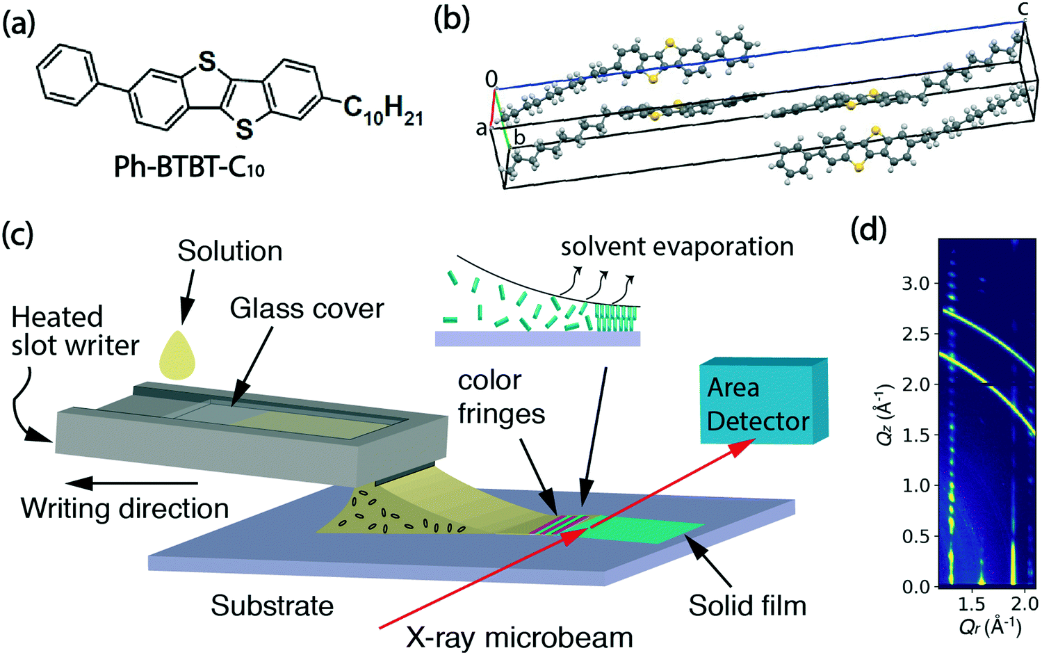 | ||
| Fig. 1 (a) The chemical structure of Ph-BTBT-C10. (b) The molecular arrangement of the bulk crystalline structure. (c) Set-up of the in situ X-ray experiment. A motion-controlled microslot writer is used to hold the solution and write the film. In order to show the details, the meniscus is amplified and not to scale compared to the writer. The incident X-ray microbeam and scattered X-rays are indicated by red arrows. (d) An example of the two dimensional X-ray diffraction image of a crystalline thin film as a function of the in-plane component of the wavevector transfer Qr and the component perpendicular to the substrate surface Qz. Normally, the X-ray image would not have many reflections at higher Qz when the film is just written at high temperatures, since the sharp peaks at higher Qz indicate a highly crystalline film with long-range ordering in the layer stacking direction. | ||
Heavily doped n-type (100) silicon wafers with 300 or 330 nm of thermally grown silicon oxide were used as substrates for the fabrication of bottom-gate, top-contact OFETs and for the X-ray measurements. Phenyltriethoxy silane (PTS) (98%) was purchased from Sigma Aldrich and used for substrate treatment to improve the wettability and reduce surface charge traps.17
2.2 Microslot writer
The thin film deposition was performed using a custom microslot writer, which utilizes a direct writing method with guidance of the solution meniscus. It is a scaled up version of our previous pen writer based on a 5 × 1 mm2 rectangular glass capillary. In this new implementation, the bottom half of the capillary is replaced by a stainless-steel slot writer, while a glass cover slide encloses a narrow reservoir where the solution to be deposited is held by surface tension. The horizontal reservoir is 1′′ × 3′′ and the vertical channel has a narrow opening of 0.5 mm, with a 10 mm-wide protruding slot. A schematic of the writing process showing the internal details of the channel and the reservoir is shown in ESI† Fig. S1. The design has certain advantages of a standard slot-die apparatus since the solution is only deposited on the surface when the writer and substrate are in motion relative to each other. However, unlike a slot-die it does not require the solution to be actively pumped since it is fed entirely by gravity-assisted surface interactions. The microslot writer was heated by attaching a polyimide heating tape to the bottom surface. During film deposition, the writer was heated at 60 °C to increase the solubility of Ph-BTBT-C10 in chlorobenzene. Computer-controlled linear translation stages (Newport, M-VP-25XA) were used to either move the substrate or the writer at controlled speeds in the range 0.01–25 mm s−1.2.3 In situ polarized microscopy and ex situ profilometry
Real-time polarized optical microscopy (Olympus BXFM) was utilized to study the sequence of phases formed and the evolution of the grain morphology with the substrate moving during slot writer deposition. Film thickness was measured by a Dektak XT stylus profilometer.2.4 In situ GIXD characterization
In situ microbeam grazing incidence X-ray diffraction (GIXD) was carried out during the solution deposition process at the soft matter interfaces beamline (12-ID SMI) at the National Synchrotron Light Source II (NSLS II).18 Scattering patterns were measured at 16.1 keV with an incidence angle of 0.1°, a beam size at the sample position of 2.5 μm × 25 μm (V × H) and recorded on a Pilatus 300 kW detector, consisting of 0.172 mm square pixels in a 1475 × 195 array, mounted at a fixed distance of 274.9 mm from the sample position. To cover the range of scattering angles desired, the vertically oriented elongated detector was positioned at a fixed arc of 11.5 degrees. The two-dimensional scattering patterns were later visualized in Xi-CAM software and converted into Q-space using a custom Python code.19 The in situ X-ray series was taken at 0.1 second per frame for the deposition process and post-deposition time series was taken at 1 second per frame. Scattering patterns were collected from an adjacent area of the film at the completion of post deposition scans in order to assess radiation damage. No discernible degradation was observed for X-ray exposures up to at least 20 minutes.A schematic of the real-time experiment layout is shown in Fig. 1(c). In this experiment, the writer is motion-controlled and the X-ray beam remains fixed on the same spot on the substrate to observe the entire process of crystallization from liquid solution. The inset illustrates the crystallization happening at the trailing edge of the meniscus where color fringes appear as the solvent evaporates.
2.5 OFET device fabrication and characterization
Transistors were made on solvent-cleaned and PTS-treated substrates. The procedures are: ultrasonication in deionized water, acetone and isopropanol for 10 minutes respectively, followed by treatment in a 3.0 wt% PTS solution of toluene for 15 hours at 110 °C, and finally rinsed with toluene, acetone and isopropanol. The Ph-BTBT-C10 thin films for transistors were deposited using a smaller capillary writer of 0.5 mm × 5.0 mm opening size.20 The capillary writer was utilized without heating at a substrate speed of 25 mm s−1 and substrate temperature of 90 °C with solution in chlorobenzene of 6 mg ml−1. Arrays of gold source and drain electrodes were thermally evaporated through a shadow mask onto the organic semiconductor, with a channel length of 30 μm and a width of 1000 μm to form a bottom gate top contact OFET. The 330 nm silicon oxide serves as the gate dielectric layer with capacitance Ci = 9.09 nF cm−2. The electrical measurements were carried out on a Cascade M150 probe station with Keithley 2636 Source Meter. Four transistors fabricated with the same film were measured to calculate the reported average mobility. Fig. 5 shows results for one of them.3 Results
Fig. 2 shows the comparison between the scattering patterns of the crystalline state and the smectic-E phase. The crystalline state was measured after cooling the sample to room temperature and waiting for 12 hours. As shown in Fig. 2(a), the periodic sharp peaks in the high Qz range at Qr = 1.31 Å−1 indicate a highly crystalline film. The Q-spacing ΔQz ≈ 0.115 Å−1 is estimated from the spacing along (11 L) in Fig. 2(a), leading to a layer spacing d ≈ 54.6 Å. This value is comparable to the single crystal value c = 53.124 Å reported by Minemawari et al.15 The crystalline unit cell is a double-layered structure along the c-axis, which leads to a doubling in the reciprocal space map along the Qz direction relative to the smectic-E phase. This doubling is clearly observed in the Qz positions of crystalline (11 L) reflections in Fig. 2(c). The β angle is estimated to be 93.6° from the Qz of (110) position in Fig. 2(c). Thus, our data is consistent with a monoclinic phase with a = 6.08, b = 7.87, c = 54.6, and β = 93.6°. These values are in close agreement with the bulk structure reported in the literature.15 We note that the two partial rings in the Q range between 2.6 and 3.0 Å−1 are consistent with unintentional scattering from the sample holder.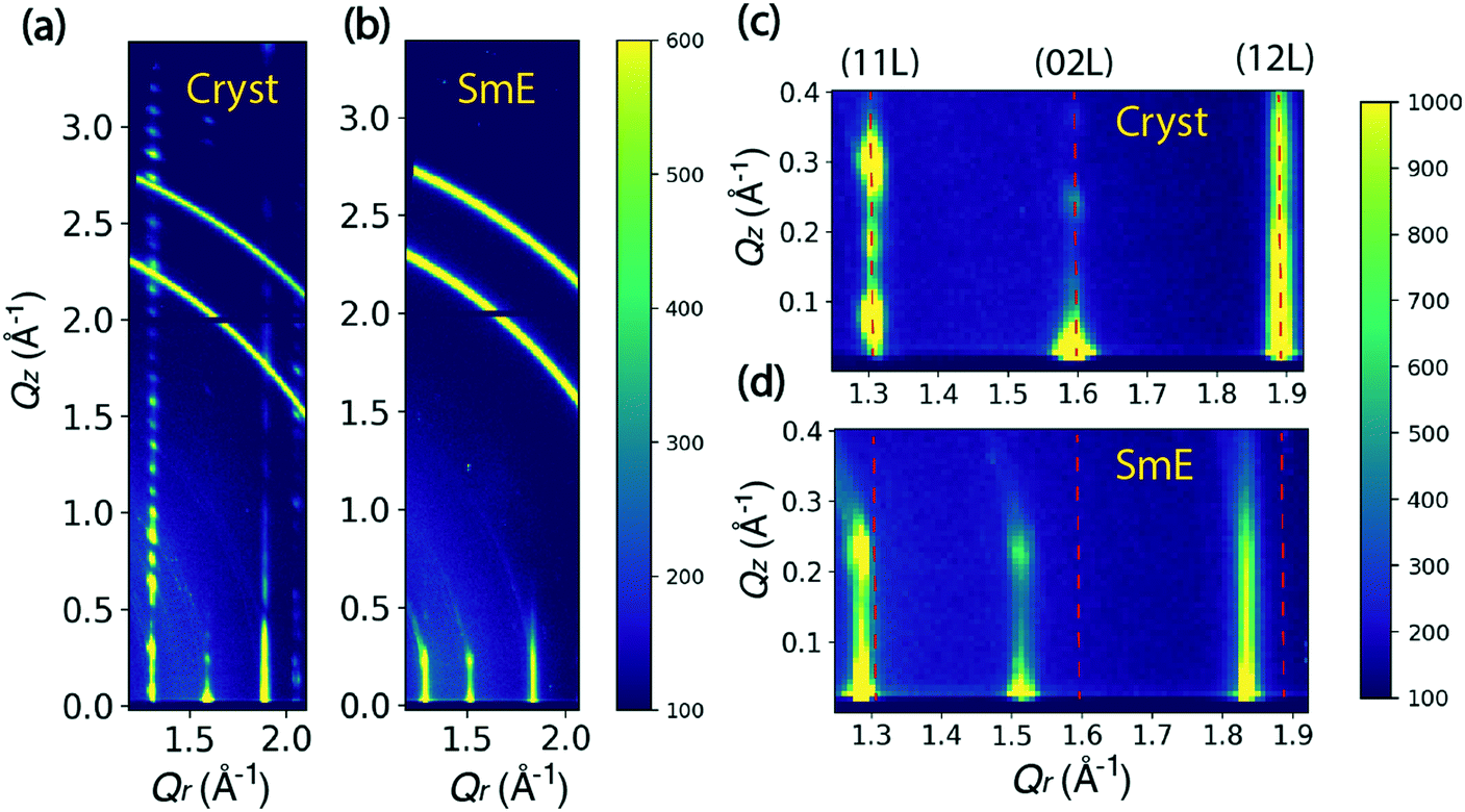 | ||
| Fig. 2 The sample was made at 90 °C and 12.5 mm s−1. It was then cooled to room temperature for about 12 hours. The crystalline state is measured during annealing at 70 °C in (a and c) and the smectic-E phase is observed while annealing at 155 °C in (b and d). (a) The crystalline phase observed at 70 °C. The three columns of bright peaks are assigned to (11 L), (02 L) and (12 L). A weaker-intensity column at Qr = 2.07 Å−1 is assigned to (20 L). ΔQz ≈ 0.115 Å−1 is estimated from the spacings of (11 L) in a wide Qz range, corresponding to a double layer spacing of Δd ≈ 54.6 Å. (b) A smectic-E phase observed at 155 °C with the same sample, ΔQz ≈ 0.22 Å−1 is estimated from the sharp peaks of (02 L), leading to a monolayer spacing of Δd ≈ 28.6 Å. (c and d) are zoomed in from (a) and (b) respectively. The labeled columns in (c) at Qr = 1.31, 1.6, 1.89 Å−1 shift to Qr = 1.29, 1.52, 1.84 Å−1 in (d). The Qz positions of (11 L) show roughly double peaks in (c), indicating a transformation from a double-layer crystalline lattice to single-layer structure of the smectic-E phase in (d). | ||
The smectic-E phase was observed when the sample was annealed at 155 °C after the crystalline state was measured. For comparison, Fig. 2(b) shows that there is limited long-range order, for which scattering peaks in the high Qz range are absent due to the large vibrational amplitudes of the molecules and reduced correlations between the layer positions. The streaks indicate a correlation length of only a few unit cells. However, since several periodic reflections are observed along Qz, the smectic-E phase is more properly classified as crystal smectic-E.21 The ΔQz spacing is changed to 0.22 Å−1, estimated from the Qz positions of the crystal smectic-E (02 L) at Qr = 1.52 Å−1 in Fig. 2(d), which leads to d ≈ 28.6 Å. This is close to the literature value of c = 29.1 Å, and consistent with a monolayer phase.22 Comparing the Qr positions in Fig. 2(c and d), the crystal smectic-E phase has smaller Qr positions for the three labeled columns. Thus, our data is consistent with a rectangular monolayer-crystal smectic E phase with a = 6.04 Å, b = 8.27 Å, c = 28.6 Å, and α = β = γ = 90°. This is in good agreement with results in the literature.22 Below, we refer to the rectangular monolayer-crystal smectic-E phase as Sm-E for simplicity, and to avoid confusion with the monoclinic crystalline phase.
Fig. 3 shows the results of an in situ thin film deposition study of Ph-BTBT-C10 at 90 °C and 0.2 mm s−1 with 11 mg ml−1 solution in chlorobenzene. Fig. 3(a) shows the last frame of the 75 second time series, which is 40 seconds after most X-ray reflections first appear. The in-plane positions of several rods match the Sm-E phase at (11 L), (02 L) and (12 L) in Fig. 2(d) and there are no sharp peaks present in higher Qz region of image, which is consistent with a smectic phase. We tracked the intensities of the whole in-plane region to see how the peak intensities change with time. Fig. 3(b) shows a close-up view of the two regions of interest corresponding to Qz = 0.16–0.18 Å−1 and 0.03–0.05 Å−1 respectively, as indicated by the two red boxes. The intensities in the red boxes are summed and shown as 2D images and 1D curves over time respectively in Fig. 3(c and d) and 3(e and f). The two regions of interest show different intensity features over time. The crystalline and Sm-E peaks are labeled based on our measurements shown in Fig. 2. However, the Tr label in Fig. 3(e and f) refers to transient phases, since these peak positions cannot be assigned to either the Sm-E phase or crystalline phase directly. For simplicity, we assume that the transient phases are only minor modifications of the Sm-E phase, so that they can be indexed according to the closest Sm-E or crystalline peak positions. For instance, Tr (11 L) at Qr =1.32 Å−1 matches the crystalline phase in the Qr direction, but without doubling of sharp peaks in the Qz direction like in Fig. 2(c). Thus, this Tr (11 L) indicates the transient phase where molecules are likely organized with long-range ordering similar to the crystalline phase in the plane of the film, but still exhibit a single monolayer unit cell in the perpendicular direction. Another remarkable feature is that the weak Tr (11 L) rod appears in coincidence with the solution ring during the deposition, as shown in Fig. 3(d) and in the real-time X-ray diffraction images at 32.5 second and beyond [ESI† Fig. S2(a and b)]. Optical studies reported in Fig. 4 are consistent with the X-ray data, since the ordering is observed to begin while there is still significant solvent present. Thus, the co-existence of diffraction peaks and the solution ring indicate the co-existence of the ordered phase and the solvent. This diffraction peak possibly stems from critical nucleation happening at the top surface of the thinning meniscus front, which can be distinguished through grazing-incidence X-ray diffraction. The buried interface between the solution and substrate does not contribute to the diffraction signal since the penetration depth of 16.1 keV X-ray at a grazing incidence of 0.1° is estimated to be 110 nm (see the calculation in the ESI†) while the meniscus is at least several micrometers thick, based on separate optical microscopy measurements. However, most of the rods with strong intensity appear immediately after the solvent ring has disappeared, as labeled with orange dashed lines in Fig. 3(c and d). This could indicate that some or most of the film is forming at the buried substrate–solution interface, so that it is not detected while the solution ring is present. Alternately, the film may be ordering right at the contact line between the solution and substrate, but the optical studies reported in Fig. 4 do not exhibit a well-defined contact line, which makes this possibility seem less likely.
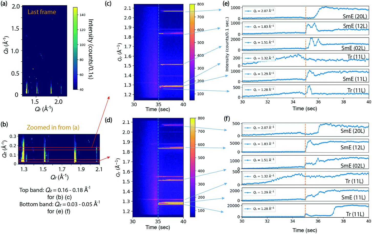 | ||
| Fig. 3 Observation of real-time deposition for Ph-BTBT-C10 solution in chlorobenzene written at 0.2 mm s−1 and 90 °C. The film thickness is 170 ± 20 nm. (a) GIXD image of the films at the end of the time series at 75 seconds and zoomed in at lower Qz in (b). The top and bottom red boxes in (b) indicate two regions of interest at Qz = 0.15–0.17 Å−1 and 0.03–0.05 Å−1 respectively, whose intensities are traced over time in (c) and (d) respectively. (e and f) The corresponding intensity plots versus time for certain Qr positions as the arrows point to, for Qz = 0.15–0.17 Å−1 and 0.03–0.05 Å−1 respectively. The vertical dash lines in (c–f) indicate the time when the solution meniscus passes the X-ray beam, and thus the newly deposited film is detected. Tr stands for transient phase. | ||
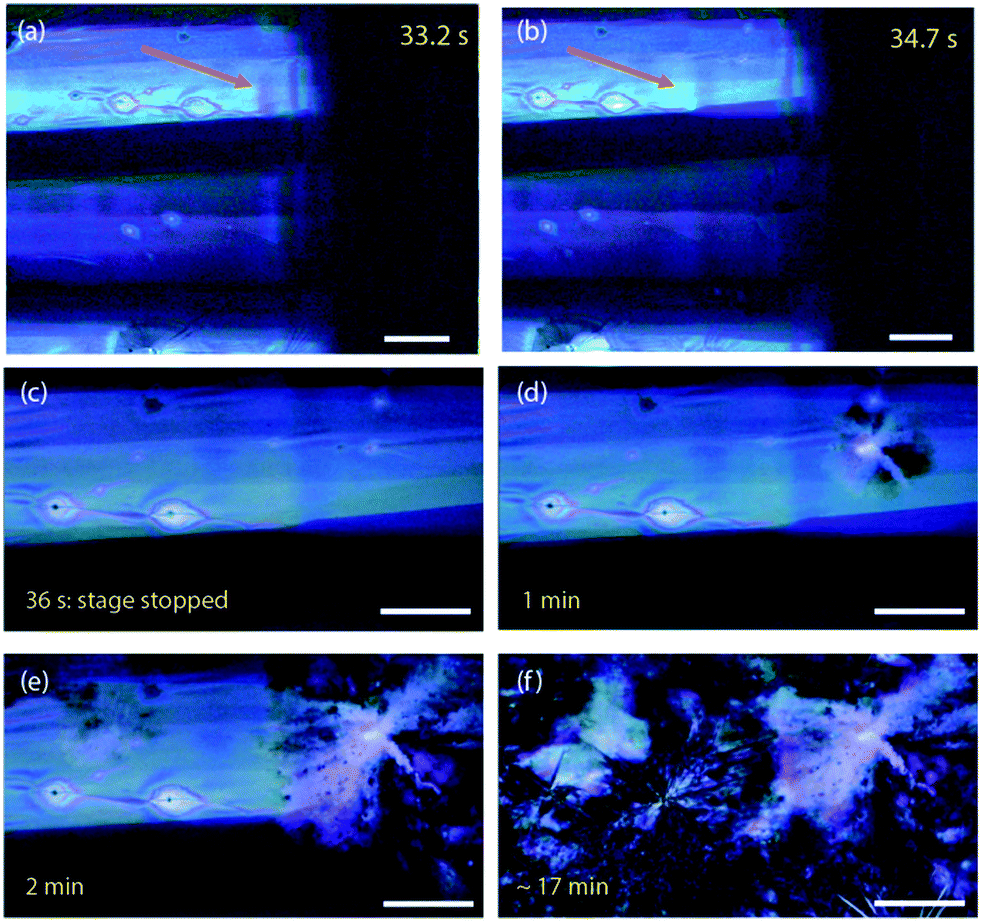 | ||
| Fig. 4 Frames from a polarized optical microscopy video during deposition at 90 °C with solution in chlorobenzene and 0.2 mm s−1 writing speed. The white scale bar is 200 μm. (a) and (b) The arrow points to the same spot on the film, showing where the color fringes are evolving into a solid film. The translational stage stops at (c) t = 36 s after the region of the film shown is written. The initial film has long stripe-like grains. (d) Some nucleation sites appear on the film. (e) The nucleation sites slowly grow larger and replace the original aligned grain structures. (f) The film has stopped changing around 17 minutes when temperature was held at 90 °C. The final film thickness was approximately 450 nm. | ||
A striking feature of the data in Fig. 3 is that during the first 1–2 seconds after the solvent ring is gone, the intensity oscillates up and down for Sm-E (02 L) and Sm-E (12 L) in Fig. 3(e) within the region Qz = 0.16–0.18 Å−1 and in Fig. 3(f) in the lower Qz region of 0.03–0.05 Å−1, although they appear to be less pronounced in the lower Qz range. We do not interpret these features as being due to layer-by-layer growth, which would exhibit extended periodic oscillations. Rather, the fluctuations are a clear signature of domain fluctuations of the thin film. In addition, the (20 L) intensity in Fig. 3(e and f) has a delayed onset in both Qz ranges, which is evidently related to the fluctuations. A possible scenario is that sub-critical nuclei of the double-layer crystalline phase are forming and disappearing. We note that the doubling crystalline peaks that would appear around Qz = 0.16–0.18 Å−1 are never clearly observed in these early stages, but the fluctuating intensity may be an indication of crystalline-like domains forming and then shrinking again. Another, perhaps more likely scenario is that transient phase domains compete with each other and grow or shrink via the motion of domain boundaries. The oscillations continue only as long as excess solvent remains in the film. The fact that the film subsequently stays in the transient or smectic states for an extended time is associated with the asymmetric molecules and the nature of the Sm-E phase that only allows molecular oscillations with angles less than 180°.23,24 In other words, the molecules are greatly inhibited from flipping end-over-end, which is one route to forming the double-layer structure of the crystalline phase.
The real-time study in Fig. 3 shows that the film deposited at 90 °C did not transform into the crystalline phase at the end of the time-series. Moreover, there was no indication of the crystalline phase even after more than 20 minutes post deposition while the substrate was held at 90 °C, even thought the crystalline phase is the equilibrium phase at that temperature. On the other hand, when a similar experiment was performed at 80 °C, the deposited film exhibits some transient phases closer to the crystalline phase (ESI† Fig. S3). In that case, the as-deposited film presented peaks in the higher Qz of 0.6–1.0 Å−1 and some weak streaks at the position of doubling crystalline peaks. (Qz ≈ 0.18 Å−1 at Qr ≈ 1.3 Å−1) Thus, the transient phases at 80 °C are more ordered than the Sm-E phase at 90 °C, which indicates the nucleation barrier is temperature dependent. We reported in our previous work on C8-BTBT that the nucleation barrier gets higher as the deposition temperature approaches the phase transition temperature, exhibiting a longer incubation time and lower nucleation rate subsequently.8 This observation is consistent with the classical nucleation theory.25 In addition, these transient phases at 80 °C show intensity fluctuations along with an unusual diffuse ring appearing and disappearing in a 20 minute post-deposition period (ESI† Fig. S4). It is very unusual for a disordered phase with diffuse ring to appear from a relatively ordered phase. However, we note that the thin film did not fully transform to a crystalline thin film within the 20 minute time interval of the scan, in spite of the significant changes. Below, we turn to polarized optical microscopy results, which show a clearer observation of the formation of the final crystalline phase.
The GIXD observations are complimented by a real-time movie series of the deposition process using a polarized microscope. In Fig. 4, six frames from the polarized microscope series for deposition at 90 °C substrate temperature are presented. In this experiment, the substrate was translated at a controlled speed of 0.2 mm s−1 while the slot writer was kept still. We note that the solvent does not show polarization contrast because it is isotropic and it appears dark with crossed polarizers because polarization microscopy is a dark field mode. This allows us to “look through” the solvent to see the thin film forming underneath. The thin film is visible even within the meniscus due to it's strong polarization contrast. The images reveal several things: (i) the thin film is optically biaxial due to the unit cell in the a–b plane being elongated in the b direction, (ii) the Sm-E phase forms long, oriented stripe-like domains with alternating contrast, and (iii) the Sm-E phase coexists with un-evaporated solvent, appearing to form at the substrate surface beneath the solvent meniscus. In Fig. 4(a and b), the arrow points to the same part of the film, showing the color fringes in Fig. 4(a) that disappear with time. It takes around 1 second to go across the fringe region at 0.2 mm s−1, consistent with the intensity fluctuations observed in the X-ray peaks right after the solution ring disappears. As a result of the coexistence between the Sm-E phase and the solution phase, there is no well-defined contact line between the solid film and the solution meniscus. The moving stage carrying the sample stops at t = 36 seconds, shown in Fig. 4(c), when the whole view is freshly written in long strips of Sm-E or transient phase grains. A nucleation event occurs in Fig. 4(d) on the top right corner, and subsequently the aligned film is gradually consumed by a large spherulitic grain, as shown in Fig. 4(e and f). This morphology transition is interpreted as a phase transformation of the Sm-E phase, showing as aligned stripe domains, most likely to the crystalline phase or some transient phases that are closer to the crystalline phase. It is notable that the original aligned grain structure is replaced, which indicates that the crystalline phase is not inherited from the Sm-E phase to induce the herringbone structures, as has been suggested in previous work.16,22
The hole mobility of Ph-BTBT-C10 is evaluated through the measurement of top-contact bottom-gate transistors fabricated with solution-processed Ph-BTBT-C10 thin films. Usually, slow processing speeds are favored over fast speeds, since slow speeds lead to large grain size and fewer grain-boundary related defects. However, as we observed in Fig. 4, the initial aligned large grains of Ph-BTBT-C10 thin film deposited at slow speed were replaced with large spherulitic grains due to the phase transformation of the meta-stable Sm-E phase. The re-nucleation removes the motivation to deposit at slow speeds since the original aligned grain structure is wiped out. Therefore, we deposit thin films in the fast processing regime for transistor fabrication. We find that thin films written at 25 mm s−1 and 90 °C exhibit uniform polycrystalline grains formed through renucleation that are large enough to cover our transistor channel length of 30 μm (ESI† Fig. S5). The large grain size is achieved due to the low nucleation rate at temperatures close to the bulk phase transition temperature. In other words, the slow transformation rate can be taken advantage of since it leads to a controllable, large grain size. Notably, fast processing is necessary for high-throughput manufacturing organic semiconductor thin films in large area through the roll-to-roll process.
Fig. 5(a and b) shows the output and transfer characteristics of a representative Ph-BTBT-C10 transistor in top-contact bottom-gate structure with the capillary-pen-written films processed at 25 mm s−1 and 90 °C. A polarized microscope image of the film is shown in Fig. 5(c) as an inset. For this transistor, a saturation mobility of 3.76 cm2 V−1 s−1 is extracted from the transfer curve in Fig. 5(b), taken from a measurement made at 24 hours after it was fabricated. Fig. 5(d) shows that the saturation mobility did not degrade from 24 to 120 hours. In Fig. 5(c), the linear mobility of this transistor is shown as 2.86 cm2 V−1 s−1 at Vd = −5 V and 120 hours, which is smaller than the saturation mobility. This is also true for the average saturation mobility of 2.4 cm2 V−1 s−1 and the average linear mobility of 2.0 cm2 V−1 s−1 among 4 transistors on the same Ph-BTBT-C10 film. This slight discrepancy is attributed to the contact resistance that manifests itself as non-linear current at very small drain voltage in Fig. 5(a). The contact resistance can become comparable to the channel resistance at small Vd and can affect the estimated channel mobility.26
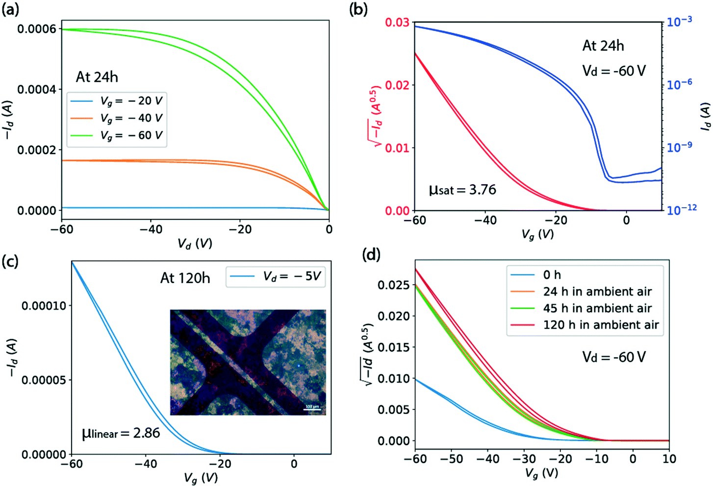 | ||
| Fig. 5 (a) and (b) Output and transfer characteristics of a typical Ph-BTBT-C10 transistor in top-contact bottom-gate structure with pen written films processed at 25 mm s−1 and 90 °C from a solution in chlorobenzene of 6 mg ml−1. (c) The linear mobility measured for the same transistor at Vd = −5 V and 120 hour, at which point the saturation mobility is the same as at 24 hour. The inset image shows the corresponding transistor with film under polarized microscope. Film thickness is 30 nm. (d) The transfer characteristics at different times after it was made. | ||
In Fig. 5(d), it is shown that the drain current of the Ph-BTBT-C10 transistor changes significantly in the first 24 hours. A possible explanation is related to an anomalous aging effect associated with the Schottky contact at the metal/semiconductor interface, which has been observed in the C8-BTBT top-contact transistors.26 Since the HOMO level of Ph-BTBT-C10 (ref. 27) is similar to C8-BTBT, a Schottky contact is likely to be formed. This aging model interprets the performance at 0 hour as suppressed by insufficient charge injection, resulting from trapped charge in the contact region. According to our previous findings from transistors fabricated with C8-BTBT as the active layer, a series of light-activated effects release the trapped charge and improve the contact over a period of hours. Here, we have shown that high mobility is obtained with Ph-BTBT-C10 thin films processed at fast speed with the bi-layer crystal phase, which is confirmed by the X-ray reflections and optical series. However, we can not rule out the possibility that some of the observed change in the transistor current is due to a slow phase change, which can be very slow as we have shown above.
4 Discussion
Fig. 6 shows models of the structural difference between the crystalline phase and the Sm-E phase. In the crystalline phase shown in Fig. 6(a), the asymmetric molecules are oriented alternating directions in adjacent layers to form a double-layered lattice. We argue that in the liquid crystal phase, relatively ordered packing may occur due to the strong interaction between the molecular cores while leaving the side-groups disordered as shown in Fig. 6(b). This results in randomness in the molecular orientations with some having an up-configuration and others having a down-configuration. The disorder within the layers changes the double unit cell into a single unit cell. To have the metastable transient phases form first in a two-step transformation, the transient phases must have lower activation barriers for nucleation compared to the stable phase.28 If we think in terms of symmetry breaking, the transition to a less ordered state such as a layered transient phase involves less symmetry breaking compared to the fully crystalline state. This leads to lowered activation barriers for nucleation of the lower symmetry phase since the Gibbs free energy has an entropy term and higher entropy corresponds to lower free energy. An alternative picture that we can not entirely rule out is that at least some of the transient phases are stable during the time that they coexist with extra solvent, consistent with a remnant metastability type model. However, this would depend on the existence of stable lyotropic phases that have not been identified so far. Given that phases close to or identical to the high-temperature Sm-E phase shown in Fig. 2(b and d) dominate the transient phases, the model that we have described above involving Ostwald's rule of stages, free energy barriers, and symmetry breaking is better supported by the available experimental data.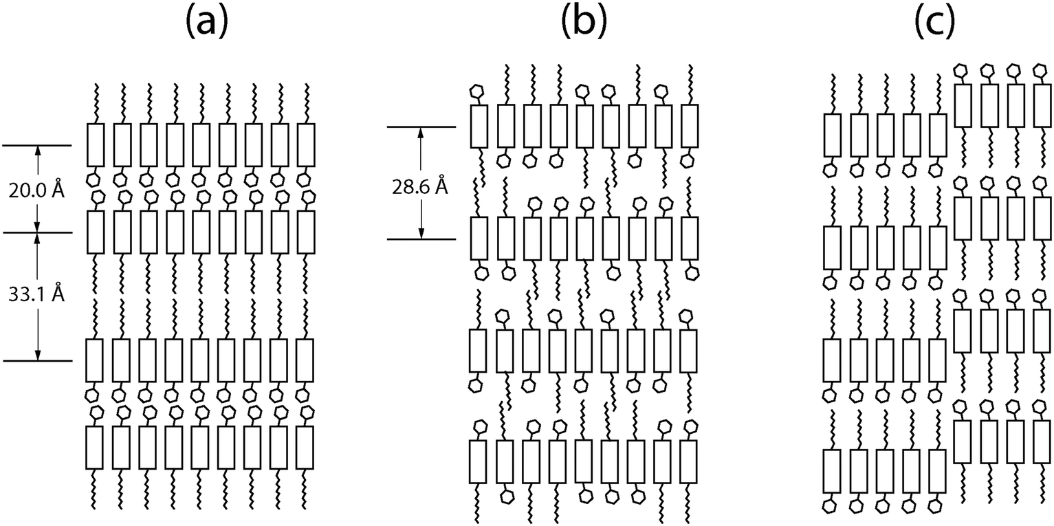 | ||
| Fig. 6 A schematic illustration of models for the molecular arrangement in different phases. (a) The crystalline phase with a bilayer structure. (b) An intermediate smectic phase with random up/down orientations of the asymmetric molecules before the Sm-E domains grow. (c) The Sm-E domains in a nanosegregated monolayer structure with anti-parallel grain boundaries. | ||
We can estimate the Sm-E phase domain size from the peak width ΔQr in Fig. 3. The width ΔQr of 0.01 Å−1 would indicate a domain size of at least 62.8 nm. This implies that the structure of completely random up/down molecular orientations in Fig. 6(b) likely acts as a precursor to form larger Sm-E domains. Our structural model for the Sm-E domains is illustrated in Fig. 6(c). It is a nanosegregated monolayer structure with anti-parallel grain boundaries similar to the antiparallel monolayer crystal model in the literature, but with a larger domain size.29 Simulated hole mobility shows that the antiparallel monolayer has only 0.14 times the mobility of the bilayer structure.29 This is consistent with the reported experimental mobilities of the Sm-E phase and crystalline phase.16 Evidently, the antiparallel configuration acts as a significant bottleneck to charge carrier transport. Note that molecular diffusion within each layer occurs at a much faster rate compared to inter-layer diffusion.30 Thus, it is energetically favorable to grow the single-layer Sm-E domains through intra-layer diffusion from Fig. 6(b) to Fig. 6(c). Regarding the transition from Sm-E phase to the crystalline phase, the possible routes are to flip half of the molecules in each layer or to diffuse molecules between the layers in Fig. 6(c). However, both routes involves a large energy barrier and slow kinetics, and hence, both processes are thought to be very slow,30 consistent with the slow transformation that we have observed.
5 Conclusions
In summary, we have observed that meta-stable liquid crystal and transient phases are formed before reaching the final crystalline phase in the crystallization process of Ph-BTBT-C10 from solution when the deposition temperature is below the phase transition temperature. Multiple co-existing transient phases are observed through X-ray diffraction, and they fluctuate in time, possibly by the motion of domain walls. For certain conditions, the crystal nucleation is delayed for an extended period of time, which is attributed to the high energy barrier associated with symmetry breaking required for the formation of the double layer structure. We have also observed that the crystalline phase re-nucleates from the Sm-E phase, forming spherulitic grains. Our studies develop a deeper understanding of the crystallization mechanisms and controlling nucleation for small molecule semiconductors with liquid crystal phases and asymmetric molecules. Moreover, the delayed nucleation and lowered nucleation rates can lead to grain size larger than the transistor channel length, which is beneficial for reproducible transistor performance, and to methods to control or select the final structural phase of the thin film for further device optimization. These capabilities may be exploited for applications in diverse areas ranging from neuromorphic electronics to nonvolatile memories based on organic semiconductors.Conflicts of interest
There are no conflicts to declare.Acknowledgements
This work was supported by the National Science Foundation, Division of Materials Research, Electronic and Photonic Materials Program through award award DMR-1701774. This research used the SMI beamline (12-ID) of the National Synchrotron Light Source II, a U.S. Department of Energy (DOE) Office of Science User Facility operated for the DOE Office of Science by Brookhaven National Laboratory under Contract No. DE-SC0012704. The authors thank Prof. Mathew White for his assistance on film thickness measurement.References
- Y. Yu, Q. Ma, H. Ling, W. Li, R. Ju, L. Bian, N. Shi, Y. Qian, M. Yi and L. Xie, et al., Small-molecule-based organic field-effect transistor for nonvolatile memory and artificial synapse, Adv. Funct. Mater., 2019, 29(50), 1904602, DOI:10.1002/adfm.201904602.
- H. Ling, S. Liu, Z. Zheng and F. Yan, Organic flexible electronics, Small Methods, 2018, 2(10), 1800070, DOI:10.1002/smtd.201800070.
- J.-L. Brédas, D. Beljonne, V. Coropceanu and J. Cornil, Charge-transfer and energy-transfer processes in π-conjugated oligomers and polymers: A molecular picture, Chem. Rev., 2004, 104(11), 4971, DOI:10.1021/cr040084k.
- J. L. Brédas, J. P. Calbert, D. A. da Silva Filho and J. Cornil, Organic semiconductors: A theoretical characterization of the basic parameters governing charge transport, Proc. Natl. Acad. Sci. U. S. A., 2002, 99(9), 5804, DOI:10.1073/pnas.092143399.
- S. T. Bromley, M. Mas-Torrent, P. Hadley and C. Rovira, Importance of intermolecular interactions in assessing hopping mobilities in organic field effect transistors: pentacene versus dithiophene-tetrathiafulvalene, J. Am. Chem. Soc., 2004, 126(21), 6544, DOI:10.1021/ja049762a.
- S. Fratini, D. Mayou and S. Ciuchi, The transient localization scenario for charge transport in crystalline organic materials, Adv. Funct. Mater., 2016, 26(14), 2292, DOI:10.1002/adfm.201502386.
- S. Karthika, T. Radhakrishnan and P. Kalaichelvi, A review of classical and nonclassical nucleation theories, Cryst. Growth Des., 2016, 16(11), 6663, DOI:10.1021/acs.cgd.6b00794.
- J. Wan, Y. Li, J. G. Ulbrandt, D.-M. Smilgies, J. Hollin, A. C. Whalley and R. L. Headrick, Transient phases during fast crystallization of organic thin films from solution, APL Mater., 2016, 4(1), 016103, DOI:10.1063/1.4939464.
- W. Ostwald, Studies on formation and transformation of solid materials, Z. Phys. Chem., 1897, 22, 289 CrossRef CAS.
- T. Threlfall, Structural and thermodynamic explanations of Ostwald's rule, Org. Process Res. Dev., 2003, 7(6), 1017, DOI:10.1021/op030026l.
- D. Gebauer, M. Kellermeier, J. D. Gale, L. Bergström and H. Cölfen, Pre-nucleation clusters as solute precursors in crystallisation, Chem. Soc. Rev., 2014, 43, 2348, 10.1039/C3CS60451A.
- D. Erdemir, A. Y. Lee and A. S. Myerson, Nucleation of crystals from solution: Classical and two-step models, Acc. Chem. Res., 2009, 42(5), 621, DOI:10.1021/ar800217x.
- B.-R. Chen, W. Sun, D. A. Kitchaev, J. S. Mangum, V. Thampy, L. M. Garten, D. S. Ginley, B. P. Gorman, K. H. Stone and G. Ceder, et al., Understanding crystallization pathways leading to manganese oxide polymorph formation, Nat. Commun., 2018, 9(1), 1, DOI:10.1038/s41467-018-04917-y.
- W. Sun, S. T. Dacek, S. P. Ong, G. Hautier, A. Jain, W. D. Richards, A. C. Gamst, K. A. Persson and G. Ceder, The thermodynamic scale of inorganic crystalline metastability, Sci. Adv., 2016, 2(11), e1600225, DOI:10.1126/sciadv.1600225.
- H. Minemawari, J. Tsutsumi, S. Inoue, T. Yamada, R. Kumai and T. Hasegawa, Crystal structure of asymmetric organic semiconductor 7-decyl-2-phenyl[1]benzothieno[3,2-b][1]benzothiophene, Appl. Phys. Express, 2014, 7(9), 091601, DOI:10.7567/apex.7.091601.
- H. Iino, T. Usui and J.-I. Hanna, Liquid crystals for organic thin-film transistors, Nat. Commun., 2015, 6(1), 6828, DOI:10.1038/ncomms7828.
- I. Cour, P. V. Chinta, C. M. Schlepütz, Y. Yang, R. Clarke, R. Pindak and R. L. Headrick, Origin of stress and enhanced carrier transport in solution-cast organic semiconductor films, J. Appl. Phys., 2013, 114(9), 093501, DOI:10.1063/1.4820384.
- Advances in Computational Methods for X-Ray Optics III, ed. M. Zhernenkov, N. Canestrari, O. Chubar, E. DiMasi, I. M. S. del Rio and O. Chubar, International Society for Optics and Photonics, SPIE, 2014, vol. 9209, pp. 133–141, DOI:10.1117/12.2060889.
- R. J. Pandolfi, D. B. Allan, E. Arenholz, L. Barroso-Luque, S. I. Campbell, T. A. Caswell, A. Blair, F. De Carlo, S. Fackler, A. P. Fournier, G. Freychet, M. Fukuto, D. Gürsoy, Z. Jiang, H. Krishnan, D. Kumar, R. J. Kline, R. Li, C. Liman, S. Marchesini, A. Mehta, A. T. N'Diaye, D. Y. Parkinson, H. Parks, L. A. Pellouchoud, T. Perciano, F. Ren, S. Sahoo, J. Strzalka, D. Sunday, C. J. Tassone, D. Ushizima, S. Venkatakrishnan, K. G. Yager, P. Zwart, J. A. Sethian and A. Hexemer, Xi-cam: a versatile interface for data visualization and analysis, J. Synchrotron Radiat., 2018, 25(4), 1261, DOI:10.1107/S1600577518005787.
- S. Wo, R. L. Headrick and J. E. Anthony, Fabrication and characterization of controllable grain boundary arrays in solution-processed small molecule organic semiconductor films, J. Appl. Phys., 2012, 111(7), 073716, DOI:10.1063/1.3698203.
- S. Hofer, W. Bodlos, J. Novák, A. Sanzone, L. Beverina and R. Resel, Molecular packing analysis of the crystal smectic E phase of a benzothieno-benzothiophene derivative by a combined experimental/computational approach, Liq. Cryst., 2021, 1–9, DOI:10.1080/02678292.2021.1907626.
- H. Iino and J.-I. Hanna, Liquid crystal and crystal structures of a phenyl-benzothienobenzothiophene derivative, Mol. Cryst. Liq. Cryst., 2017, 647(1), 37, DOI:10.1080/15421406.2017.1289427.
- S. Diele, P. Brand and H. Sackmann, X-ray difraction and polymorphism of smectic liquid crystals. ii. D and E modifications, Mol. Cryst. Liq. Cryst., 1972, 17(2), 163, DOI:10.1080/15421407208083838.
- M. Luzar, A. M. Thayer and A. Pines, Zero field N.M.R. of uniaxial and biaxial smectic liquid crystals, Mol. Phys., 1987, 62(3), 573, DOI:10.1080/00268978700102411.
- D. A. Porter and K. E. Easterling, Phase transformations in metals and alloys (revised reprint), CRC press, 2009 Search PubMed.
- J. Wan, Y. Li, J. Hollin, A. C. Whalley, W. Matthew and R. L. Headrick, Eliminating light-induced aging effects and non-linear carrier injection in organic semiconductor thin film transistors, Unpublished manuscript, 2021 Search PubMed.
- S. Park, B. Lee, B. Bae, J. Chai, S. Lee and C. Kim, Ambipolar thin-film transistors based on organic semiconductor blend, Synth. Met., 2019, 253, 40, DOI:10.1016/j.synthmet.2019.05.001.
- S.-Y. Chung, Y.-M. Kim, J.-G. Kim and Y.-J. Kim, Multiphase transformation and Ostwald's rule of stages during crystallization of a metal phosphate, Nat. Phys., 2009, 5(1), 68, DOI:10.1038/nphys1148.
- M. Yoneya, Monolayer crystal structure of the organic semiconductor 7-decyl-2-phenyl[1]benzothieno[3,2-b][1]benzothiophene, revisited, Jpn. J. Appl. Phys., 2020, 59(9), 090909, DOI:10.35848/1347-4065/abb00e.
- A. Baggioli, M. Casalegno, G. Raos, L. Muccioli, S. Orlandi and C. Zannoni, Atomistic simulation of phase transitions and charge mobility for the organic semiconductor Ph-BTBT-C10, Chem. Mater., 2019, 31(17), 7092, DOI:10.1021/acs.chemmater.9b02882.
Footnote |
| † Electronic supplementary information (ESI) available. See DOI: 10.1039/d1me00078k |
| This journal is © The Royal Society of Chemistry 2022 |