
 Open Access Article
 This Open Access Article is licensed under a Creative Commons Attribution-Non Commercial 3.0 Unported Licence
Effect of quantum confinement on polarization anisotropy emission in Sn-doped CdS microcones†
Ye
Tian
 ab,
Shangfei
Yao
a,
Wenchao
Lin
a,
Hui
Peng
*a,
Yongyou
Zhang
*b and
Bingsuo
Zou
*a
ab,
Shangfei
Yao
a,
Wenchao
Lin
a,
Hui
Peng
*a,
Yongyou
Zhang
*b and
Bingsuo
Zou
*a
aGuangxi Key Lab of Processing for Nonferrous Metals and Featured Materials and Key lab of new Processing Technology for Nonferrous Metals and Materials, Ministry of Education, School of Resources, Environments and Materials, Guangxi University, Nanning 530004, China. E-mail: penghuimaterial@163.com; zoubs@gxu.edu.cn
bBeijing Key Laboratory of Nanophotonics & Ultrafine Optoelectronic Systems, Beijing Institute of Technology, Beijing 100081, China. E-mail: yyzhang@bit.edu.cn
First published on 21st October 2022
Abstract
Polarization anisotropy of emission, which carriers a lot of effective information that cannot be obtained from light intensity, wavelength, frequency and phase, is promising for multifunctional applications ranging from optical communication to spectroscopy analysis. The manipulation of polarization emission at room temperature is essential for spintronic applications. However, most of the high degree polarization is achieved at cryogenic temperatures or using sophisticated epitaxial techniques. Here, we prove the relationship between the cross-section radius and polarization ratio, and demonstrate the maximum polarization ratio is about 60% when the cross-section radius is 1.15 μm in a Sn-doped CdS microcone. Time-resolved PL spectra provide insight into radiative contributions to the observed polarization emission. In addition, the emission peak of free exciton A (FXA) is blue-shifted with the decrease of cross-section radius, which proves that the quantum confinement effect plays an important role in the observed polarization anisotropy emission. Our work provides a promising approach to achieve room temperature high-spin polarization, which contributes to spin-photonics applications.
Introduction
In recent years, one-dimensional (1D) nanostructures have shown many unique properties for a wide range of applications to waveguide devices, nano-sensors, light-emitting diodes, etc.1,2 The optical properties of semiconductor nanostructures can be tuned by engineering their size, morphology, and composition.3 Designing new structures with unique polarization properties has attracted much interest, which can store information and control device operations.4,5With the development of quantum information science, strong polarization anisotropy nanostructures are required to broaden their application.6–8 During the past years, various works on polarization routers have been reported. Researchers reported that reducing the emission lifetime can increase the polarization emission of nanostructures.9,10 Most of the high degree polarization is achieved at cryogenic temperatures or by 2D heterostructures.11–13 For example, Zhang et al. reported high-spin polarization in 2D layers by reducing the carrier lifetime via the heterostructure.14 Chen et al. reported light-induced spin polarization in transition metal dichalcogenide nanostructures and their heterostructures at cryogenic temperatures.15 Although large spin polarization can be obtained in this way, complex material transfer technology is required. Therefore, the adjustment of polarization emission without sophisticated epitaxial techniques at room temperature has always been a challenge in a nanostructure.
CdS nanostructures show great potential for polarization optoelectronic applications due to their large exciton binding energy and large crystal anisotropy.16,17 Due to the anisotropy of material and geometry, the emission intensity of different polarizations is very different, which makes them appealing elements for polarization sensitive devices.18 The generation and control of the degree of spin polarization are the keys for the device applications. However, there are few systematic studies on polarization in CdS nanostructures due to the limitations of nanostructures and measurement. Adjusting the carrier lifetime is an effective way to achieve high spin polarization. The unique quantum confinement effect in nanostructures provides an effective route to manipulate the carrier lifetime. Therefore, it is ideal to find a new mechanism to obtain high spin polarization by manipulating the carrier lifetime at room temperature, which is very important for practical spintronic application. The lifetime of photogenerated carriers is shortened by size adjustment, and it is proved that PbI2 has nearly 100% spin polarization at room temperature.14 Thus the size of nanostructures affect the energy of emission peaks and radiative recombination lifetime. A deep understanding of the size and scattering effects on the recombination dynamics of CdS nanostructures is a key step for the design of polarization related nanodevices and the effect of the radius on their polarization behavior has not yet been investigated.
Here, we report the realization of room temperature high spin polarization in Sn-doped CdS microcones. TRPL spectra show that the emission lifetime reduces with the decrease of microcone cross-section radius. Due to the decrease of carrier lifetime, it is observed that the maximum degree of polarization is 60% when the cross-section radius is 1.13 μm at room temperature. The polarization related to emission can be controlled by the radius of microcones, which provides a means of control for further practical application. In addition, cross-section radius-dependent ARPL spectra were recorded and it was found that FXA blue-shifts with the decrease of microcone cross-section radius, which indicates that high spin polarization is related to the surface induced quantum confinement effect. This work provides not only a basis for controlling the carrier dynamics and spin polarization in CdS nanostructures, but also a strategy for realizing high spin polarization at room temperature.
Experimental section
Materials and preparation
The Sn-doped CdS microcones were synthesized by chemical vapor deposition with SnO2 as the catalyst. Possible growth processes for these Sn-doped CdS microcones are schematically shown in Fig. S1 (ESI†). The morphology, size and shape of the microcones could be controlled by growth temperature, gas velocity and the SnO2/CdS ratio.Characterization
The morphology and microstructure of the Sn-doped CdS microcones were characterized by scanning electron microscopy (SEM, Zeiss SUPRA 55). X-ray photoelectron spectroscopy (XPS) was performed on a ULVAC-PHI Quantera II. The micro-photoluminescence (micro-PL) spectra and PL lifetime were measured with a commercial near-field scanning optical microscope (NSOM) (WITec alpha300) system using 405 nm He–Cd lasers. Angle-resolved photoluminescence (ARPL) imaging experiments were performed using an angle-resolved spectroscopy system (Shanghai Idea-optics Technology).Fig. 1a shows the scanning electron microscopy (SEM) morphology of the microcone on a transparent SiO2 wafer, which shows a uniform and smooth surface and a big ball on the top. The cross-section radius ranges from 0.4 μm to 3.5 μm and the length is about 102.15 μm. The inset tables give the contents of different elements in the top and backbone of the microcone. Fig. 1(h) and (i)–(k) provide the elemental contents and distributions at the top of the microcone, respectively. This shows that the top ball is mainly composed of Sn. Fig. 1(n) and (e)–(g) provide the elemental contents of Cd, S, and Sn and distributions of the three elements in the middle of the microcone structure, respectively. This shows that the Sn is doped into the nanostructure though EDS with a sensitivity of 1%.19 Fig. S2(a) (ESI†) shows the wide scan XPS spectrum of Sn-doped CdS samples, which indicates that Sn is indeed doped into CdS nanostructures. The narrow scan XPS spectra of Cd, S and Sn are shown in Fig. S2(b)–(d) (ESI†). In addition, the nanostructure has a big sphere on the top, revealing its vapor–liquid–solid (VLS) growth mechanism.20,21 In this CVD process, Sn, instead of common Au, acts as a catalyst. From the above morphology characterization, high quality Sn doped CdS microcone structures were synthesized.
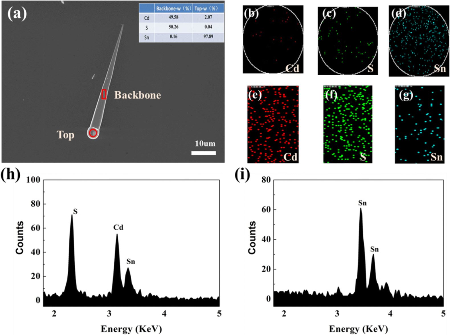 | ||
| Fig. 1 (a) High magnification SEM image of the Sn-doped CdS microcone. (b–d) Cd, S and Sn element mapping at the top. (c–g) Cd, S, and Sn element mapping at the backbone. (h and i) EDS spectra at the backbone and top of the microcone structure. | ||
To demonstrate the radius dependent carrier lifetime, we have performed time-resolved PL spectroscopy by the time-correlated single photon counting (TCSPC) method. A 405 nm pulsed laser was used to excite the sample, and a 600 short-pass filter was used to collect the emitted PL photons. The influence of cross-section radius on the recombination rate in a single Sn-doped CdS microcone was investigated. The lifetimes of the Sn-doped CdS microcone at different radii was measured from the same sample under the same experimental conditions. We found that the carrier lifetime increases slightly as the radius becomes larger, which can be attributed to the diffusion and re-excitation processes in the Sn-doped CdS microcone. Fig. 2(a) shows the PL decay curves of the Sn-doped CdS microcone with a typical cross-section radius, in which the lifetime changed from 1.51 to 5.45 ns when the radius changes from 1.15 μm to 3.39 μm. With the cross-section radius decrease, the surface to volume ratio will become much higher, which may induce trapping of more nonradiative excitons.22 Upon photoexcitation, a hole with a large effective mass would be mostly localized in the core, and a relatively light electron would delocalize significantly into the surfaces. The reduced wave function overlapping between the hole and electron of an exciton would thus increase the radiative lifetime of the exciton.23Fig. 2(b) shows that the increase of the PL lifetime with the radius became significantly pronounced as the radius increased, which indicated that the difference in wave function confinement of the photogenerated electron and hole in the microcone increases. With the increase of the cross-section radius, the carrier recombination rate caused by the defect state effect becomes increasingly lower, so that we can observe an increasingly longer exciton recombination life.24
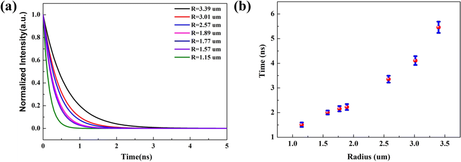 | ||
| Fig. 2 (a) TRPL spectra of a Sn-doped CdS microcone with different cross-section radii. (b) Lifetimes of the Sn-doped CdS microcone with different cross-section radii. | ||
To probe the effect of the cross-section radius on the polarization emission, we performed circularly polarized PL spectroscopy at different radii on a Sn-doped CdS microcone. By adding a polarizer in the collection optical path, the PL spectra at different polarization angles can be collected. Fig. S3(a) and (b) (ESI†) shows the polarization-dependent PL spectra and polarization-dependent Raman spectra, which indicated that the PL spectra and Raman spectra change with the polarization angle. Accordingly, the polarization emission is related to the anisotropy of the microcone. Fig. 3(a) displays the circularly polarized PL spectra with the radius varying from 1.15 μm to 3.39 μm. For the PL signal from the microcone, besides the overall dominating emission with 0° polarization (black), the weak emission signal from the 90° polarization (red) can be observed. For linearly polarized light, the polarization properties can be described by the degree of polarization, which represents the difference between the strongest (Imax) and weakest (Imin) light intensity values at the polarization detection angle, and the value is (Imax − Imin)/(Imax + Imin).25 The degree of polarization ρ at different radii can be calculated based on the obtained polarized PL spectra as shown in Fig. 3(b). As the radius of the microcone decreases from 3.39 μm to 1.15 μm, the degree of polarization of the Sn-doped CdS microcone increases from 24.39% to 61.52%. Although there are small deviations that may be due to the coupling between the anisotropy of the microcone, in general, we observed a trend that the smaller the radius, the higher the degree of polarization. In addition, the spectra showed that, with the decrease of the radius of the microcone, the emission peak gradually blueshifted.26,27 These changes are related to the PL emission of different excitons. The emission peak gradually blueshift are consistent with the radius-dependent carrier lifetime that the reduction in carrier lifetime in the microcone, which leads to the increase in the circular PL polarization emission.
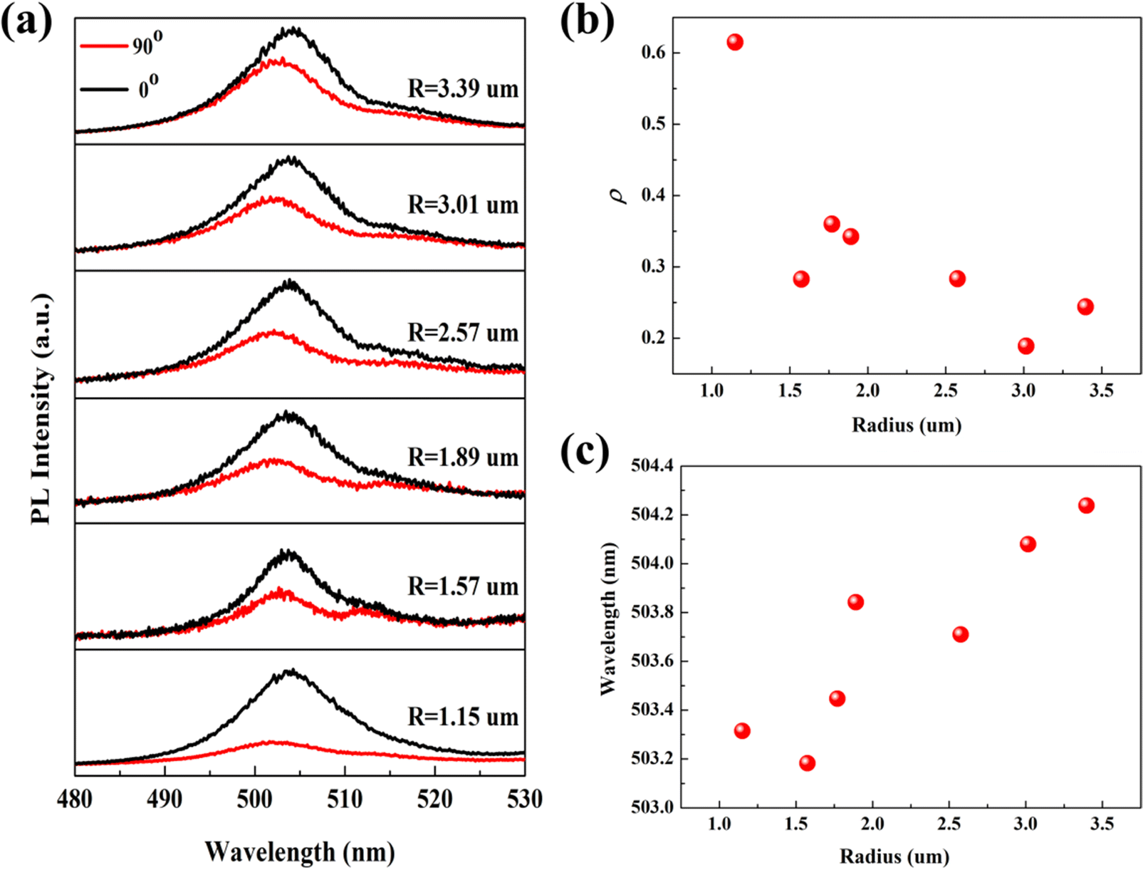 | ||
| Fig. 3 (a) Radius-dependent circularly polarized PL spectra of a Sn-doped CdS microcone. (b) The degree of polarization related to the cross-section radius of the Sn-doped CdS microcone. (c) The wavelength shift related to the cross-section radius of the Sn-doped CdS microcone. | ||
Traditionally, there are two main mechanisms proposed for interpreting the giant linear polarization, which include the quantum size effect and the optical confinement effect.28 Both of these mechanisms depend on the sizes of nanostructures. However, for the case of the quantum size effect, the size dependence not only determines the degree of polarization but also affects the emission energy. From the size-dependent measurements, the emission peak is blueshifted from 504.23 nm to 503.31 nm as shown in Fig. 3(c). We also listed the PL peak wavelengths at different polarization degrees, the degrees of polarization and PL lifetimes at different radii in Table 1. The relationship between the radius of the microcone and its luminescence peak energy is explained in detail, which indicates that the peak energy of PL depends on the diameter of the microcone. Although conventional spectroscopic measurements can be employed to characterize the optical properties of these nanostructures, information of different excitons obtained in this way is limited. Meanwhile, as the shift of the emission peak is about 1 nm, it is not obvious and the spectra of different excitons are mixed together; the origin of polarization emission needs to be further discussed.
| R (μm) | 0° wavelength (nm) | 90° wavelength (nm) | ρ (%) | Time (ns) |
|---|---|---|---|---|
| 3.39 | 501.73 | 504.23 | 24.39 | 5.45 |
| 3.01 | 502.26 | 504.08 | 18.89 | 4.11 |
| 2.57 | 502.39 | 503.71 | 28.31 | 3.36 |
| 1.89 | 502.12 | 503.84 | 34.24 | 2.23 |
| 1.77 | 502.12 | 503.44 | 36.02 | 2.16 |
| 1.57 | 501.73 | 503.18 | 28.25 | 2.01 |
| 1.15 | 501.60 | 503.31 | 6152 | 1.51 |
In order to explore the influence of cross-section radius on the emission peak, we used ARPL spectroscopy to comprehensively understand the optical properties of the Sn-doped CdS microcone. Here, two collection configurations, in which the c-axial direction of the microcone nanostructure is parallel or perpendicular to the entrance slit of the monochromator when the longitudinal axis of the entrance slit is fixed, where φ and θ are the photon collection angles in the two collection configurations, were adopted; see Fig. 4(a) and (f).29,30Fig. 4(b) and (g) show the ARPL spectra of the microcone in the two configurations, which show two emission peaks of free exciton A (FXA) and free exciton B (FXB).31,32 ARPL spectra at five different cross-section radii when the excitation power is 54 mW are shown in Fig. 4(a–j), and the microcone is perpendicular (Fig. 4(a–e)) and parallel (Fig. 4(f–j)) to the slit, respectively. The conduction band and valence band movement is not obvious at 54 mW, which makes a reasonable quantitative comparation of the radius-dependent ARPL spectra. In the two configurations, the FXA emission blueshift is obvious with the decrease of cross-section radius. The cross-section radius-dependent PL spectra were extracted from the ARPL spectra at 40° with the microcone perpendicular to the slit as shown in Fig. 4(m). Two vertical dashed lines indicate the position shift of FXA and FXB. The FXB emission peaks of the different cross-section radii are all around 506 nm at 54 mW, while FXA blueshifts from 521.6 nm to 516 nm with decreasing cross-section radius as shown in Fig. 4(n). Therefore, the cross-section radius has a great influence on the emission of FXA. The particle-in-a-box model has been used frequently to describe the blueshift of the exciton emission peak: ΔE = h2π2/2msR2,33 where h is the Planck constant, ms is the effective mass of FXA, and R is the cross-section radius of the microcone nanostructure. Fig. 4(o) shows a comparison between the experimental data and the theoretical results of FXA emission energy with 1/R2, which showed that the theoretical equation is well consistent with the experimental data. The linearity of the 1/R2 dependence of the FXA emission energy can be ascribed to the size depletion induced quantum confinement effect. As the emission energy of FXA blueshifts with the decrease of cross-section radius, the reason for the change of polarization in this paper is attributed to the quantum confinement effect.
 | ||
| Fig. 4 (a) Schematics of ARPL imaging, where the microcone is parallel to the entrance slit of the monochromator. (b–f) ARPL images with the cross-section radius ranging from 3.39 μm to 1.15 μm. The microcone is set to be parallel to the entrance slit of the monochromator. (g) Schematics of ARPL imaging, where the microcone is perpendicular to the entrance slit of the monochromator. (h–l) ARPL images with the cross-section radius ranging from 3.39 μm to 1.15 μm. The microcone is set to be perpendicular to the entrance slit of the monochromator. (m) PL spectra of the microcone with the cross-section radius ranging from 3.39 μm to 1.15 μm. The spectra extracted from ARPL spectra at 40° with the microcone being parallel to the entrance slit of the monochromator. (n) The wavelength shift related to cross-section radius with an excitation power of 54 mW. (o) Comparison between the experimental data and the theoretical results of FXA energy as a function of the cross-section radius of the Sn-doped CdS superlattice microcone. | ||
Conclusions
In conclusion, high quality Sn-doped CdS microcones were synthesized by a simple CVD method. Using the circular polarization PL spectra and time-resolved PL spectra, we prove that the circular polarization emission is enhanced due to the reduction of cross-section radius. A maximum of 60% polarization of the Sn-doped CdS microcone is observed at room temperature. The underlying physics relies on the reduction of the carrier lifetime with the decrease of the cross-section radius of the Sn-doped CdS microcone. In addition, we also found that the emission peaks of FXA blue-shifts with the decrease of cross-section radius using the ARPL spectra. Therefore, the enhancement of circularly polarized emission is related to the surface induced quantum confinement effect. Our work proposes a method to adjust the circular PL polarization emission of Sn-doped CdS nanostructures through size changes without introducing chiral organic cations at room temperature, which is helpful to the application of CdS based spintronic devices.Author contributions
Writing, methodology, review, and editing: Ye Tian; formal analysis and investigation: Shangfei Yao and Wenchao Lin; visualization and supervision: Hui Peng and Yongyou Zhang; funding acquisition and project administration: Bingsuo Zou.Conflicts of interest
The authors declare no conflicts of interest.Acknowledgements
The authors thank the Guangxi NSF project (2020GXNSFDA238004), the National Natural Science Foundation of China (Grant No. 12074037) and the “Guangxi Bagui Scholars” Foundation for financial support.References
- R. Yan, D. Gargas and P. D. Yang, Nat. Photonics, 2009, 3, 569–576 CrossRef CAS.
- J. C. Johnson, K. P. Knutsen, H. Q. Yan, M. Law, Y. F. Zhang, P. D. Yang and R. J. Saykally, Nano Lett., 2004, 4, 197–204 CrossRef CAS.
- G. Dai, B. Zou and Z. Wang, J. Am. Chem. Soc., 2010, 132, 12174–12175 CrossRef CAS PubMed.
- Z. Li, K. Bao, Y. Fang, Y. Huang, P. Nordlander and H. Xu, Nano Lett., 2010, 10(5), 1831–1835 CrossRef CAS PubMed.
- A. Lamas-Linares, J. C. Howell and D. Bouwmeester, Nature, 2001, 412, 887–890 CrossRef CAS PubMed.
- X. Niu, X. Hu, Q. Sun, C. Lu, Y. Yang, H. Yang and Q. Gong, Nanophotonics, 2020, 9, 4839 CrossRef CAS.
- Z. Liu, Y. Zhang, W. Guo, Y. Liu, X. Hu and C. Lu, Opt. Lett., 2019, 44, 5772–5775 CrossRef CAS PubMed.
- J. Giblin, V. Protasenko and M. Kuno, ACS Nano, 2009, 3, 1979–1987 CrossRef CAS PubMed.
- H. H. Fang, B. Han, C. Robert, M. A. Semina, D. Lagarde, E. Courtade, T. Taniguchi, K. Watanabe, T. Amand, B. Urbaszek, M. M. Glazov and X. Marie, Phys. Rev. Lett., 2019, 123, 067401.1 Search PubMed.
- L. Huang, D. Zhang, C. Ge, M. He, Z. Zeng, Y. Wang, S. Liu, X. Wang and A. Pan, Appl. Phys. Lett., 2021, 119, 151101 CrossRef CAS.
- J. Ma, C. Fang, C. Chen, L. Jin, J. Wang, S. Wang, J. Tang and D. Li, ACS Nano, 2019, 13, 3659–3665 CrossRef CAS PubMed.
- H. Lu, J. Wang, C. Xiao, X. Pan, X. Chen, R. Brunecky, J. Berry, K. Zhu, M. Beard and Z. Vardeny, Sci. Adv., 2019, 5(12), 0571 Search PubMed.
- Y. Kim, Y. Zhai, H. Lu, X. Pan, C. Xia, E. Gaulding, S. Harvey, J. Berry, Z. Vardeny, J. Luther and M. Beard, Science, 2021, 371, 1129–1133 CrossRef CAS PubMed.
- D. Zhang, Y. Liu, M. He, A. Zhang, S. Chen, Q. Tong, L. Huang, Z. Zhou, W. Zheng, M. Chen, K. Braun, A. Meixner, X. Wang and A. Pan, Nat. Commun., 2020, 11, 1–8 CrossRef PubMed.
- Y. Chen, J. D. Cain, T. K. Stanev, V. P. Dravid and N. P. Stern, Nat. Photonics, 2017, 11, 431–435 CrossRef CAS.
- H. M. Fan, Z. H. Ni, Y. P. Feng, X. F. Fan, J. L. Kuo, Z. X. Shen and B. S. Zou, Appl. Phys. Lett., 2007, 91, 171911 CrossRef.
- M. Zhang, M. Wille, R. Röder, S. Heedt, L. Huang, Z. Zhu, S. Geburt, D. Grützmacher, T. Schäpers, C. Ronning and J. Lu, Nano Lett., 2014, 14, 518–523 CrossRef CAS PubMed.
- A. Lan, J. Giblin, V. Protasenko and M. Kuno, Appl. Phys. Lett., 2008, 92, 183110 CrossRef.
- J. Xu, X. Zhuang, P. Guo, Q. Zhang, L. Ma, X. Wang, X. Zhu and A. Pan, J. Mater. Chem. C, 2013, 1, 4391–4396 RSC.
- R. S. Wagner and W. C. Ellis, Appl. Phys. Lett., 1964, 4, 89–90 CrossRef CAS.
- Y. Wu and P. Yang, J. Am. Chem. Soc., 2001, 123, 3165–3166 CrossRef CAS.
- G. Pozina, L. L. Yang, Q. X. Zhao, L. Hultman and P. G. Lagoudakis, Appl. Phys. Lett., 2010, 97, 131909 CrossRef.
- X. Liu, Q. Zhang, G. Xing, Q. Xiong and T. C. Sum, J. Phys. Chem. C, 2013, 117, 10716–10722 CrossRef CAS.
- H. Wang, C. Zhang and F. Rana, Nano Lett., 2015, 15, 8204–8210 CrossRef CAS PubMed.
- A. V. Maslov and C. Z. Ning, Phys. Rev. B: Condens. Matter Mater. Phys., 2005, 72, 161310 CrossRef.
- G. Eda, H. Yamaguchi, D. Voiry, T. Fujita, M. Chen and M. Chhowalla, Nano Lett., 2011, 11, 5111–5116 CrossRef CAS PubMed.
- Y. Zhao, J. Qiao, P. Yu, Z. Hu, Z. Lin, S. La, Z. Liu, W. Ji and Y. Chai, Adv. Mater., 2016, 28, 2399–2407 CrossRef CAS PubMed.
- H. Chen, Y. Yang, H. Lin, S. Chang and S. Gwo, Opt. Express, 2008, 16, 13465–13475 CrossRef CAS PubMed.
- L. Sun, S. Sun, H. Dong, W. Xie, M. Richard, L. Zhou, Z. Chen, L. Dang and X. Shen, arXiv, 2010, 1007, 4686 Search PubMed.
- S. Gong, S. Ko, M. Jang and Y. Cho, Nano Lett., 2015, 15, 4517–4524 CrossRef CAS PubMed.
- Y. Tian, Y. Zhang, H. Peng, S. Yao, T. Huang, C. Peng, Z. Yu, S. Ge and B. Zou, J. Phys. Chem. C, 2022, 126, 1064 CrossRef CAS.
- L. Sun, D. Kim, K. H. Oh and R. Agarwal, Nano Lett., 2013, 13, 3836–3842 CrossRef CAS PubMed.
- D. Li, J. Zhang and Q. Xiong, ACS Nano, 2012, 6, 5283–5290 CrossRef CAS PubMed.
Footnote |
| † Electronic supplementary information (ESI) available. See DOI: https://doi.org/10.1039/d2ma00883a |
| This journal is © The Royal Society of Chemistry 2022 |