
 Open Access Article
 This Open Access Article is licensed under a Creative Commons Attribution-Non Commercial 3.0 Unported Licence
Ferroelectric thin films: performance modulation and application
Shan
Li
a,
Yilin
Wang
b,
Mingdi
Yang
a,
Jun
Miao
 a,
Kun
Lin
a,
Qiang
Li
a,
Xin
Chen
a,
Jinxia
Deng
a and
Xianran
Xing
*a
a,
Kun
Lin
a,
Qiang
Li
a,
Xin
Chen
a,
Jinxia
Deng
a and
Xianran
Xing
*a
aBeijing Advanced Innovation Center for Materials Genome Engineering, Institute of Solid State Chemistry, University of Science and Technology Beijing, Beijing 100083, China
bInstitute of Advanced Materials (IAM), Jiangsu National Synergetic Innovation Center for Advanced Materials (SICAM), Nanjing Tech University, 30 South Puzhu Road, Nanjing, 211816, China. E-mail: xing@ustb.edu.cn
First published on 28th May 2022
Abstract
Ferroelectric thin film materials have been widely applied in a great many fields for their robust spontaneous electric polarization and strong coupling with optical, electric and magnetic fields. In recent years, breakthrough progress has been made in the performance optimization and applications of these materials. Composition control and various types of strain can effectively regulate the performance of ferroelectric films, including ferroelectric hysteresis loop, Curie temperature, leakage current, etc., to meet the application requirements of ferroelectric devices in various fields. Flexible ferroelectric thin film devices with excellent ductility and resilience have amazing application potential in intelligent robots, wearable electronic devices and the Internet of Things, expanding the application field of ferroelectric thin film materials. We briefly introduce the fabrication processes and application prototypes of flexible ferroelectric thin films. We conclude with limitations of existing research on ferroelectric thin film materials and suggestions for further research.
1. Introduction
Ferroelectrics are materials that possess spontaneous polarization without an external electric field, and the orientations of the polarization vector can be switched with the application of an electric field.1 Thin-film ferroelectrics are important subjects of ferroelectric materials. The research on ferroelectric thin films can be traced back to the 1960s, when the development of semiconductor integration technology sparked interest in applying ferroelectric thin films to non-volatile memory devices. However, due to the immature thin-film preparation technology and the incompatibility of ferroelectric materials with semiconductor processes at that time, the research and application of ferroelectric thin-films progressed slowly. In the 1980s, the rapid development of ferroelectric thin film preparation technology broke the barrier of preparing high-quality ferroelectric thin films and laid the foundation for the development of ferroelectric thin film materials.2,3 At that stage, various structural types of ferroelectric thin film materials were prepared and investigated, such as perovskite oxides, tungsten bronze and bismuth layered oxides.4–6 Among them, perovskite-type oxide Pb(ZrxTi1−x)O3 (PZT) has attracted much attention in research studies because of its superior ferroelectric and piezoelectric properties. With the rapid development of microelectronics technology, ferroelectric thin-film materials are added as functional components to microelectromechanical systems (MEMSs). In 1993, ferroelectric thin films were successfully integrated with Si complementary metal oxide semiconductors (CMOSs) and ferroelectric memory entered industrialization. From then on, the research on ferroelectric materials and devices has developed from single crystal devices to thin film devices, and from separate devices to integrated devices. In the following years, the application of pulsed laser deposition (PLD), magnetron sputtering, molecular beam epitaxy (MBE) and other technologies to prepare single crystal thin films has promoted research on the basic science of ferroelectric thin film materials such as BiFeO3,7 PZT,8 and BaTiO3.9 With the continuous development of microelectronics technology and large-scale integrated circuits, the development trend of miniaturization, integration and light weight of electronic devices has appeared, and the requirements for ferroelectric devices have become higher and higher, which has stimulated the continuous development of ferroelectric thin films. So far, ferroelectric thin film materials have been widely used in many fields, such as memory devices, detectors, piezoelectric MEMSs, etc.10–12With the rapid development of computational, modeling, synthesis, and characterization techniques, exotic physical phenomena and novel ferroelectric materials are constantly being discovered and explored. A superlattice is an epitaxial multilayer film structure obtained by alternately growing two or more different thin film materials, which is an effective approach to obtain excellent properties and explore new physical phenomena. The strong polarization enhancement was achieved in a three-component superlattice BaTiO3/SrTiO3/CaTiO3.13 By controlling the volume fraction of PbTiO3, the polarization value and Curie temperature can be adjusted over a wide range in the PbTiO3/SrTiO3 superlattice14 and the recovery of ferroelectricity was observed in the ultrashort period superlattice (PbTiO3)1/(SrTiO3)1.15 In ferroelectric–paraelectric superlattices, exotic physical phenomena can also be induced, such as vortex/anti-vortex structures,16 ferroelectric skyrmions17 and negative capacitance.18 In 2011, promising ferroelectric, Si-doped HfO2 ferroelectric thin films were reported by T. S. Böscke et al.,19 which opened the exploration of HfO2-based ferroelectric thin film materials. Although the origin of ferroelectric properties is still ambiguous, HfO2-based ferroelectric thin film materials with the advantages of simple composition elements, low dielectric constants, good ferroelectric properties even at the nanometer scale, and full compatibility with silicon semiconductor processes are expected to be applied in high-performance microelectronic devices in the future.20–22
Ferroelectric thin film materials have broad application prospects in many fields, but there are very few ferroelectric thin film devices that can be commercialized at present, because the performance of many ferroelectric thin film materials cannot meet the requirements of commercialization. Large leakage current, low nanoscale polarization value, low piezoelectric coefficient, poor cycling stability, thermal stability, etc. are the factors hindering the commercialization of ferroelectric thin film devices. Therefore, improving the performance of ferroelectric thin films is a problem to be solved in the application field of ferroelectric thin film materials. In this Review, based on the excellent work published, we introduced the rational modulation approaches for the properties (Section 2), and the application field (Section 3) of ferroelectric thin film materials. Flexible ferroelectric thin films are free from the constraint of the substrate and have excellent ductility and resilience, expanding the application fields of ferroelectric thin film materials. The fabrication processes and application prospects of flexible inorganic ferroelectric thin film materials are presented in Section 4.
2. Performance optimization
Ferroelectric thin film materials have wide application prospects in a lot of fields, but different scenarios have different requirements for performance. For example, ferroelectric memory requires superior fatigue resistance and ferroelectric sensors need robust spontaneous polarization. Hence, it is necessary to flexibly adjust the performance of ferroelectric thin film materials. In this section, we introduce some common methods for adjusting ferroelectric thin film properties.2.1 Composition control
Composition control is the most common and easiest approach to modify the structure and the properties of ferroelectric thin films. Here we review some of the effects of chemical composition control on the properties.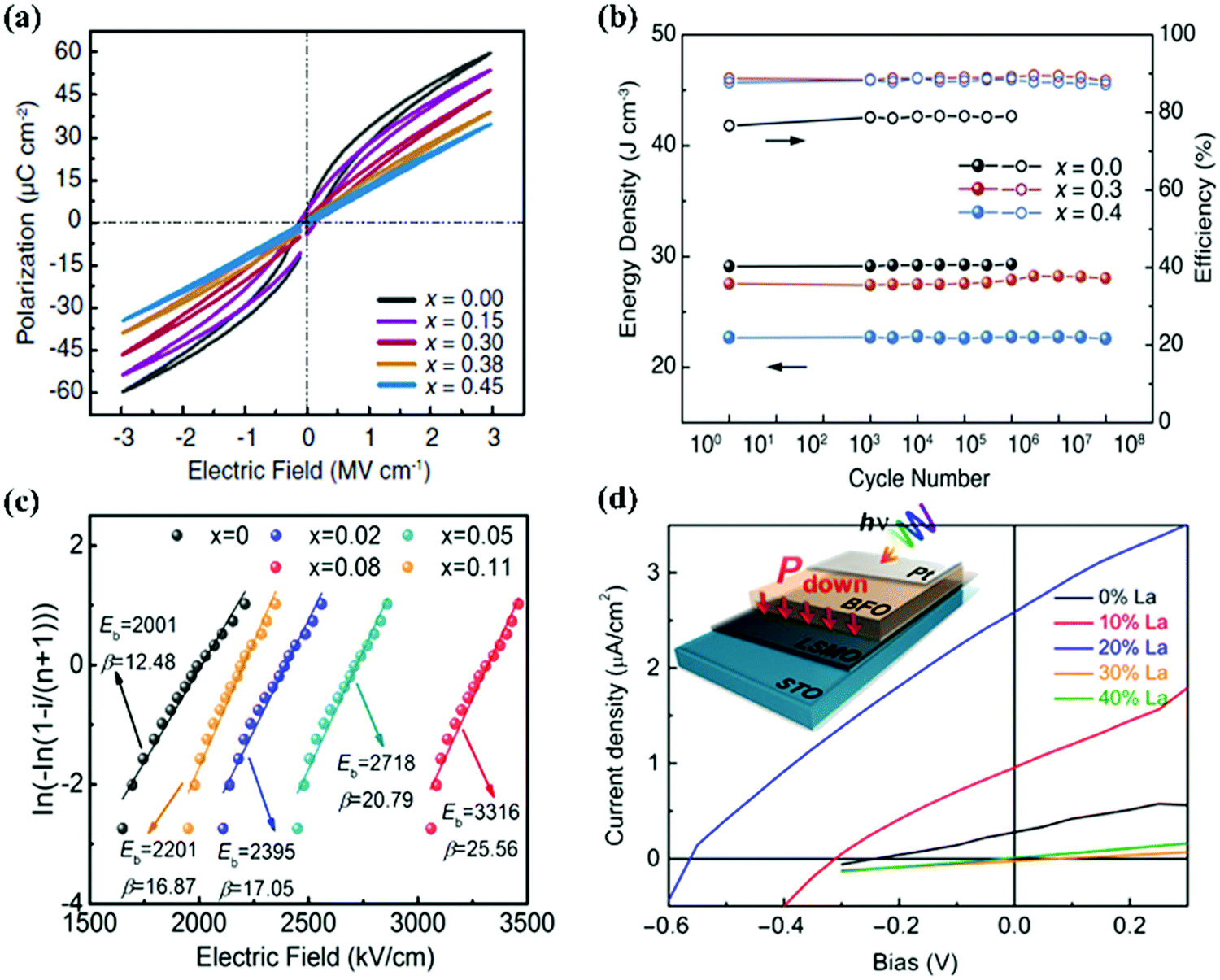 | ||
| Fig. 1 (a) The P–E curves of Sm-doped BFO–BTO thin films with various Sm content.25 (b) A cyclic fatigue test for energy storage density and efficiency of (0.55 − x)BFO–xBTO–0.45STO solid–solution thin films with various x values.26 (c) The breakdown strengths of BLT–xBFO thin films were analyzed by two-parameter Weibull distribution.27 (d) Photocurrent density–voltage curves of La-substituted BFO films.28 | ||
![[thin space (1/6-em)]](https://www.rsc.org/images/entities/char_2009.gif) 000) comparable to that of ferroelectric tunnel junctions was observed in Sm doped BiFeO3 thin films.38 The 1 mol% Mn-doped PbZr0.3Ti0.7O3 thin films showed an enhanced pyroelectric effect.39 The substitution of Pb by Sm in PbZrxTi1−xO3 thin films resulted in an unusually large piezoelectric coefficient near the Curie temperature.40 The phase transition from the polar ferroelectric phase to a nonpolar paraelectric phase exists in BiFeO3 thin films modified by rare-earth metals (La Sm, Gd, Dy), and substantial enhancement of ferroelectric photovoltaic (Fig. 1d) and electromechanical properties were observed near the phase boundaries of the nonpolar and polar phase.28,41,42
000) comparable to that of ferroelectric tunnel junctions was observed in Sm doped BiFeO3 thin films.38 The 1 mol% Mn-doped PbZr0.3Ti0.7O3 thin films showed an enhanced pyroelectric effect.39 The substitution of Pb by Sm in PbZrxTi1−xO3 thin films resulted in an unusually large piezoelectric coefficient near the Curie temperature.40 The phase transition from the polar ferroelectric phase to a nonpolar paraelectric phase exists in BiFeO3 thin films modified by rare-earth metals (La Sm, Gd, Dy), and substantial enhancement of ferroelectric photovoltaic (Fig. 1d) and electromechanical properties were observed near the phase boundaries of the nonpolar and polar phase.28,41,42
Compositional modulation can change the chemical and defect structure of materials, and plays an important role in the regulation of ferroelectric material properties, such as remanent polarization, leakage current, fatigue, and piezoelectric properties, etc. The chemical method is a universal application to modify kinds of ferroelectric thin films grown on various substrates. However, as the chemical substitution could provide limited “internal pressure”, the properties can only be modified in a narrow range. Moreover, although there are many methods for preparing thin films, few can achieve precise control of composition, and many preparation methods are not suitable for preparing thin films with complex chemical compositions.
2.2 Strain engineering
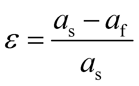
In ferroelectric materials, there is a strong coupling relationship between polarization and strain, which can be used to tailor the properties of materials.48,49 In the early 1950s, researchers studied the influence of hydrostatic pressure on the Curie temperature and dielectric properties of ferroelectric ceramics and single crystal materials.50–52 Normally, the bulk material can withstand less than 0.1% compressive and tensile strain, while thin films can tolerate approximately several percent of biaxial strain.53 The high stress tolerance of thin film materials provides a broad platform for strain control performance. The strain engineering of ferroelectric thin films has developed rapidly in the last ten decade.54–56 In particular, the construction of a stress-phase diagram (the relationship between the ferroelectric domain structure and strain) provides a good foundation for ferroelectric strain engineering. There are many ways to apply strain in thin films. Here, we briefly introduce the development of several types of strain on the properties of ferroelectric thin films.Biaxial strain arises from the lattice mismatch between the film and the substrate, and is defined as:
 | ||
| Fig. 2 (a) Misfit strain-temperature phase diagram of BTO and (b) P–E hysteresis loops of BTO thin films grown on different substrates.9 (c) Evolution of the energy (top) and c/a ratio (bottom) as a function of misfit strain for BFO thin films.7 (d) Schematic crystallographic model of vertical strain between Sm2O3 and BTO.65 (e) Tetragonality (c/a ratio) in BSTO thin films versus Sm2O3 content.66 | ||
Because of the clamping of the substrate, epitaxial strain can only be maintained within the critical thickness, restricting the efficiency of the biaxial strain in rather thick film. Due to the limitation of a high-quality single crystal substrate type, a continuously adjustable biaxial strain state cannot be achieved.
Vertical strain comes from the vertical lattice mismatch of the two materials, as shown in Fig. 2d. Vertical strain runs through the entire film thickness and could apply strain in the thick film.67 For tetragonal perovskite ferroelectric materials, the ferroelectric performance is closely related to the axial ratio. Vertical strain without constraint of the substrate can have a significant influence on the tetragonality of materials; therefore, vertical strain is an effective way to tune the performance of perovskite ferroelectric materials.65 Many rare-earth oxide, spinel and metal–oxide nanopillars were successfully assembled with perovskite oxide to achieve various properties. For example, the d33 (longitudinal piezoelectric coefficient) value of the 0.5BaTiO3:0.5Sm2O3 vertical composite thin films (45–50 pm V−1) is higher than that of pure BaTiO3 thin films and can be maintained from room temperature to 250 °C, which comes from the vertical tensile strain tuned by Sm2O3 nanopillars.68 In the (Ba0.6Sr0.4TiO3)0.25:(Sm2O3)0.75 thin films, Ba0.6Sr0.4TiO3 is subjected to vertical tensile strain controlled by Sm2O3, and the tetragonality increases with increasing thickness and Sm2O3 content (Fig. 2e).66 In the 600 nm thick film, pure Ba0.6Sr0.4TiO3 is fully relaxed, while the composite film maintains good tetragonality (c/a = 1.0112). Ferroelectric properties can be induced by vertical strain in conventional nonferroelectric materials. In composite films composed of MgO nanopillars and a SrTiO3 matrix, vertical tensile strain can be applied to the SrTiO3 lattice to achieve tetragonal distortion and induce ferroelectricity.69 SrTiO3:Sm2O3 nanocomposite thin films have been confirmed to be ferroelectric and have the merits of high dielectric tunability (49%), low dielectric loss (less than 0.01) and a high commutation quality factor (over 2800) at room temperature, making SrTiO3:Sm2O3 nanocomposite thin films suitable for microwave tunable devices.70 In vertical nanocomposite heteroepitaxial films, magnetic nanopillars with magnetostriction properties are embedded in the ferroelectric matrix, and a strong magnetoelectric coupling effect can be realized by a vertical strain coupling mechanism,71 including BaTiO3:CoFe2O4 nanostructures72 and BiFeO3:CoFe2O4 nanocomposites,73,74etc.
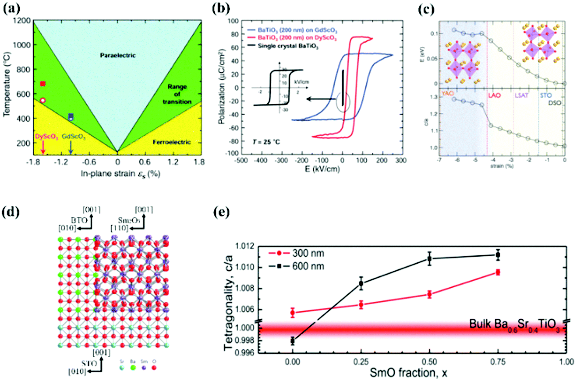
Interphase strain – Two materials with resemblant crystal structures but unequal lattice parameters were assembled into a single epitaxial composite with the same lattice constant and well-matched interface, and the strain generated at the boundaries of the two kinds of materials is the interphase strain (Fig. 3a). Interphase strain was first proposed and reported by Zhang et al. in 2018.75Fig. 3b shows the synchrotron X-ray RSMs around the (103) plane of the films and substrates. By introducing the PbO phase into a PbTiO3 epitaxial thin film, the out-of-plane crystal parameter c of the PTO composite thin films shows substantial increase, resulting in an axial ratio as large as 1.238 (that of bulk is 1.06576). The Pr value of ultra-tetragonal PbTiO3 epitaxial composite films is 236.3 μC cm−2 (Fig. 3c), which is the largest value reported to date.62 Similar structures were also obtained in BaTiO3:BaO epitaxial composite films (c-BTO).77 The cross-sectional HAADF-STEM image (Fig. 3d) of c-BTO shows that BaTiO3 and BaO have a coherent interface and that interphase strain exists between them. By calculation, the BaO lattice exerted a chemical negative pressure of −5.7 GPa on the BaTiO3 lattice, resulting in the largest tetragonal distortion (c/a = 1.12), and the P–E loops of the c-BTO (Fig. 3e) exhibit the largest Pr value of 100 μC cm−2 in BaTiO3 materials. Surprisingly, ferromagnetism was observed in the ultra-tetragonal PbTiO3 composite film. The saturation magnetic moment of 10 nm thick composite films deposited on the LaAlO3 substrate is 55 emu cc−1.78 Interphase strain can not only induce negative chemical pressure to improve ferroelectric performance but also provide a new method for the design and exploration of multiferroic materials.
 | ||
| Fig. 3 (a) Crystallographic model of interphase strain between PTO and PbO; (b) Synchrotron X-ray reciprocal space mappings (RSMs) study of PT(I), PT(II), and PT(III) epitaxial thin films around the STO (103) plane, and (c) P–E hysteresis loops of ultra-tetragonal PTO thin films;75 The cross-sectional HAADF-STEM (d) and P–E hysteresis loops (e) of c-BTO films.76 | ||
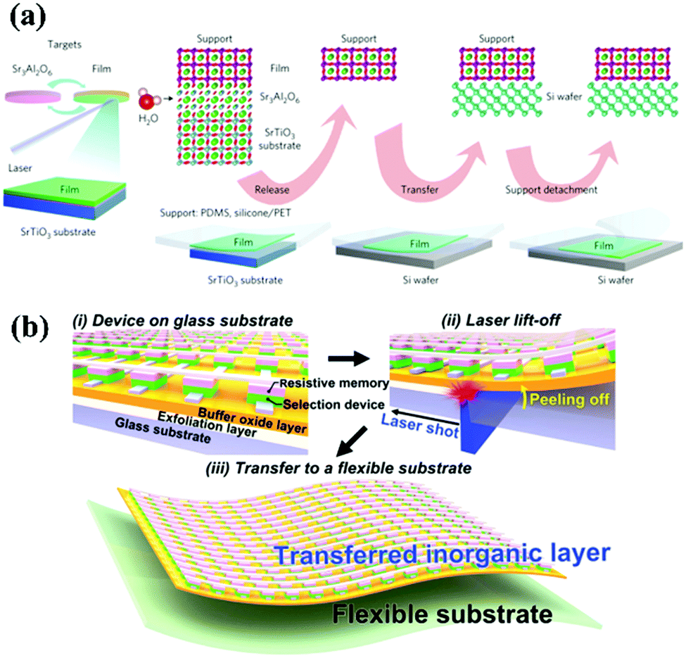
The freestanding membrane is free from the clamp of the substrate which provides a new direction for exploring the structure and properties of ferroelectric film materials. High-quantity freestanding perovskite membranes can be synthesized by the use of a sacrificial water-soluble layer (Sr3Al2O6).79,80 The perovskite thin films are deposited on substrates with Sr3Al2O6 buffer layers and placed in deionized water to remove the buffer layer, finally, transferring the membrane to the desired substrate.79 Free from the constraints of the substrate, perovskite ferroelectric membranes may exhibit some unexpected structures and properties. For example, BaTiO3 membranes show superelasticity and ultraflexibility.81 Generally, oxide ferroelectric materials are brittle, whereas a 120 nm thick BaTiO3 membrane can bear up to 10% of the mechanical bending strain without any crack, and the strain state can be recovered immediately when the 60 nm thick membrane is bent at an angle of 40° (Fig. 4a). Even when the bending angle is increased to 80°, a large part of the strain can be recovered instantly, which demonstrates the superelasticity and ultraflexibility of BaTiO3 membranes. The structural transition from an R-like phase to a T-like phase with the removal of a substrate, occurs in freestanding BiFeO3 membranes with less than four unit cells (Fig. 4b and c).82 As the thickness decreases, the axial ratio of BiFeO3 membranes increases, and the 3 unit cells of BiFeO3 membranes exhibit a remarkably large axial ratio (1.22), which is comparable to the epitaxial strain-driven T-like phase BiFeO3 thin films.62,83
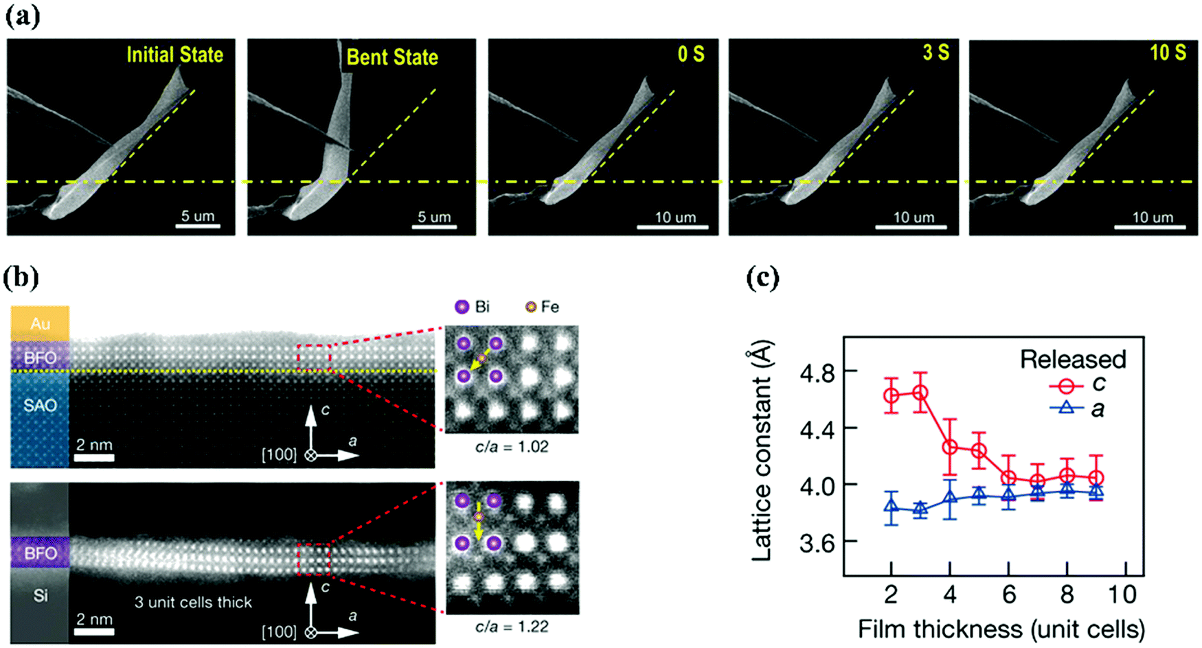 | ||
| Fig. 4 (a) SEM images of the bending and recovery process at a bending angle of 40° for a BTO nanobelt.79 (b) Cross-sectional HAADF-STEM images of a BFO thin film (three unit-cell) before (top) and after (bottom) separation from the substrate and (c) the crystal parameters a and c as a function of the freestanding BFO film thickness.80 | ||
The realization of composition control and strain engineering depends on the deposition method and thermal treatment process of the thin films. The chemical composition, defect structure and strain state of the thin films can be flexibly controlled by different deposition methods and thermal treatments, so as to achieve the adjustment of the properties. Nowadays, many deposition methods are applied to grow ferroelectric thin films. Classified by the mechanisms, the deposition methods are divided into two categories: chemical methods and physical methods. Chemical methods, including chemical solution deposition (CSD, also called sol–gel), chemical vapor deposition (CVD), etc., have strong advantages in composition regulation and are suitable for preparation of ferroelectric thin films with complex chemical composition,84,85 which can flexibly and precisely control the chemical composition. Simple instruments and easy experimental processes make chemical methods appealing. However, chemical methods generally grow polycrystal thin films, whereas physical methods are much more appealing to grow epitaxial thin films. The properties of thin films prepared by chemical methods are greatly affected by the thermal treatment process.86 Physical methods, such as atomic layer deposition (ALD), pulsed laser deposition (PLD), molecular beam epitaxy (MBE), and magnetron sputtering (MS), are widely applied to prepare high-quality ferroelectric thin films, including superlattices and ultrathin films, as these methods can in situ control the growth of crystal on an atomic level and accurately control the thickness of the film. Compared with MBE and ALD methods, MS and PLD methods have the advantage in flexible control of chemical composition and can be used to prepare the epitaxial thin films with complex compositions.36,75 The equipment of ALD and MBE are expensive, and the preparation conditions are difficult to achieve; MS can achieve large-scale preparation, but PLD cannot. These methods have different advantages and disadvantages. In order to obtain films with specific structures or properties, flexible selection of appropriate thin film deposition methods is required.
3. Application
3.1 Nonvolatile random-access memory
Ferroelectric random-access memory (FeRAM) is one of the main application fields of ferroelectric thin film materials.87 In FeRAM, two opposite polarization states of ferroelectric thin films are used for data storage.88 FeRAM has the merits of nonvolatility, fast running speed, low power consumption and irradiation resistance. FeRAM can be divided into TC-type FeRAM (including 1T1C, 2T2C, 1T2C, T: transistors, C: capacitors) and 1T-type FeFETs (ferroelectric field effect transistors) according to different storage unit structures.TC-type FeRAM works through the charge storage effect of a ferroelectric capacitor and the structure schematic diagram of the 1T1C-type FeRAM is shown in Fig. 5a.88 During the “write” operation, the polarization direction of the ferroelectric film change with the polarity of the applied electric field. Due to the self-generating stability of ferroelectric remanent polarization, the polarized charge accumulates on the electrode of the ferroelectric capacitor after removal of the applied electric field, and the two electrical properties of polarized charge are used to represent two logical states of 0 and 1. In the “read” operation, the readout voltage is applied to the ferroelectric capacitor, and the polarization reversal is judged by comparing the output current with the reference current, to determine the electrical properties of the stored charge in the ferroelectric capacitor. During this operation, the polarization direction of the ferroelectric capacitor whose polarization direction is different from the polarity of the read operation voltage, transforms to the opposite direction, which destroys the original storage state. Therefore, after the read operation, the information must be written back to restore the original storage state of the storage unit. Because the “read” process of TC-type FeRAM is destructive, the cyclic fatigue characteristics of ferroelectric films are needed.
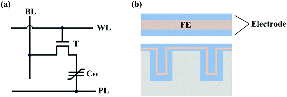 | ||
| Fig. 5 (a) Structure schematic diagram of the 1T1C-type FeRAM. (b) The schematic diagram of two-dimension (2D) planar capacitors (top) and two-dimension (3D) deep trench capacitors. | ||
Ferroelectric thin films applied in TC-type FeRAM require a high remanent polarization value, low coercive voltage and saturation polarization voltage, suitable Curie temperature and good fatigue resistance. At present, PZT- and SrBi2Ta2O9 (SBT)-based ferroelectric thin film materials are used in commercial FeRAM.89 SBT-based thin film materials have the advantage of excellent fatigue resistance.90,91 SBT-based memory has good cyclic stability and even shows a fatigue-free phenomenon after 1011 switching cycles.92 However, the low storage density due to the intrinsic low remanent polarization value (2Pr:15–20 μC cm−2), and the high integration temperature (700–800 °C) limit the development of SBT-based FeRAM.93,94 Due to the outstanding ferroelectric performance and low integrated temperature (600 °C), PZT-based ferroelectric thin films are widely used in FeRAM.95 Nevertheless, the fatigue resistance of the PZT film is poor. With the increase in the read/write cycle, a polarization decrease usually occurs at 106 cycles, which is far less than the requirement of commercial memory (1010, or even higher in special cases).94 The fatigue resistance of PZT-based capacitors can be optimized to 1011 by applying oxide electrodes (such as LiNiO3, SrRuO3, RuO2)96,97 or doping elements (such as Si, Nb, Mn),29,30 enabling the commercialization of PZT-based FeRAM.
The PZT-based embedded FeRAM technology node stagnates at 130 nm98,99 which is an order of magnitude larger than DRAM. This is due to the size effect of the perovskite ferroelectric materials. As the size of the capacitor (ferroelectric thin film thickness) decreases, the polarization value of the ferroelectric film declines, resulting in a decrease in the measurable storage charge on the electrode. According to the calculation, the remanent polarization values required for FeRAM with a stacked planar capacitor utilizing a 90 nm technology node are 2Pr > 84 μC cm−2.100 Although the Pr value of PZT is as large as 100 μC cm−2,101 the polarization value of PZT in FeRAM prepared by the semiconductor process is less than 40 μC cm−2. To reduce the technology nodes and improve the storage density, 3D capacitors are used instead of 2D planar capacitors to compensate for the area loss.102 The schematic drawing of 2D and 3D capacitors are shown in Fig. 5b.103 Yeh et al. prepared 3D PZT-based capacitors with ferroelectric properties comparable to planar devices in the laboratory.104 However, it is extremely difficult for PZT to form ferroelectric phases on sidewalls, and the idea of improving the storage density of PZT-based FeRAM by integrating 3D capacitors is still in the laboratory phase. In 2011, the discovery of HfO2-based ferroelectric materials19 made it possible to reduce the size of FeRAM. In 2014, Polakowski et al. reported 3D trench capacitors with Al-doped HfO2 thin films as ferroelectric layers.103 The Pr value based on the plane-projected area of the 3D trench capacitors with 100 k trenches is 152 μC cm−2 and the actual Pr value is 13.6 μC cm−2 which is similar to that of the 2D planar capacitor (15 μC cm−2), suggesting that any parts, including the sidewalls of the trenches, contribute to the entire polarization value. In 2019, the TiN/Hf0.5Zr0.5O3/TiN ferroelectric capacitor was successfully integrated into the 130 nm technology node back-end-of-line (BEOL) by T. Francois et al.105 The capacitor exhibited excellent performance: 30 ns operation speed, 2Pr > 40 μC cm−2, and endurance > 1011 cycles at 4 V applied voltage. HfO2-based ferroelectric materials have excellent ferroelectric properties in 3D capacitors and can be compatible with silicon CMOS (complementary metal oxide semiconductor) processes, so they are the candidate material for a new generation of FeRAM.20,106 However, a high coercive field limits the application of HfO2-based ferroelectric thin films in TC-type FeRAM. First, a high coercive electric field results in high application voltage and energy consumption. Second, the application voltage is close to the breakdown voltage, making the device vulnerable to breakdown and limiting the endurance and switching cycle.107 Therefore, reducing the operating voltage and improving fatigue resistance have been some of the main research directions of HfO2-based ferroelectric thin films.
The disadvantage of TC-type FeRAM are: the storage unit cannot be scaled down and destructive read out. The emergence of FeFETs solves these problems.
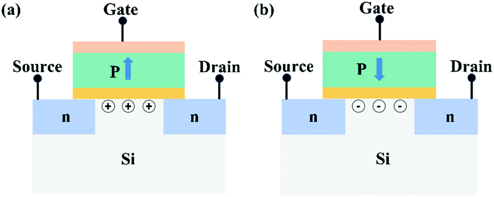
FeFET works by controlling the polarization charge of the ferroelectric layer through the gate voltage and thus modulating the conductivity of the transistor channel.108 For the N-channel enhanced FeFET (Fig. 6), in the process of “writing”, a positive/negative voltage higher than the coercive voltage of ferroelectric thin films is applied to the gate, resulting in the electrons/holes accumulating on the surface of p-type silicon and the transistor being in the on/off state. The on and off states of the transistor can be used to represent 0 and 1, respectively. In the process of “readout”, a voltage is applied between the drain and source, and the gate is suspended. If the channel is in the “on” state, the large current passes through; otherwise, no or only the small current passes through. Thus, the storage logic data can be read by comparing the size of the output current. During the readout process, the gate remains suspended, and the polarization states of the ferroelectric film is not affected. Therefore, the “readout” operation is a nondestructive reading process. FeFET has the characteristics of nondestructive readout, high storage density, and simple structure that can be scaled down. However, due to many factors, including short storage time, poor reliability, and incompatible semiconductor processes, FeFETs have not been commercialized thus far.
 | ||
| Fig. 6 Structure schematic diagram of the N-channel enhanced MFIS-type FeFET: (a) the transistor is in the off state; (b) the transistor is in the on state. | ||
According to different ferroelectric layer materials, FeFETs can be divided into PZT-based,109 SBT-based,110 LiNbO3-based111 and 2D van der Waals heterostructures.112 In this article, we focus on SBT-based and HfO2-based FeFETs. For the SBT-based FeFET devices, SBT thin films cannot be compatible with Si, so a buffer layer is grown on the surface of the semiconductor layer to avoid element diffusion and chemical reactions at the interface. The insertion of the buffer layer will bring about the voltage divider effect. Because the dielectric constant of the ferroelectric material (approximately 200) is larger than that of the buffer layer (a few decades), most of the voltage is applied to the buffer layer, resulting in incomplete polarization reversal, thus affecting the data storage time. The data retention time is one of the main parameters used to evaluate FeFET performance. The main factors affecting retention time are the depolarization field, gate leakage current and instability of the unsaturated hysteresis loop.113–115 A number of attempts have been made to solve these problems, including searching for a suitable buffer layer and ferroelectric layer materials, optimizing structural parameters, and using new structures (MFMIS, ferroelectric semiconductor–FET).115–118 A retention time of 33 days with a current rate (on/off) greater than 105 was observed in a self-aligned-gate Pt/SrBi2Ta2O9/Hf–Al–O/Si FeFET, and a current rate of 104 was extrapolated after 10 years.119 The memory window (MW) of the FeFET can be approximately given as MW = 2Ec·dFe.20 The low Ec of the SBT thin films (2Ec <0.1 MV cm−1)120 requires a large thickness to meet the memory window requirement,120,121 which limits the extensibility of SBT-based FeFETs.
Compared with SBT-based ferroelectric materials, HfO2-based ferroelectric materials have the advantages of a low dielectric constant, a high coercive electric field and full compatibility with CMOS technology,122 making it more suitable for memory applications. In particular, when the ferroelectric layer thickness is decreased, the high coercivity field can compensate for the loss of the memory window so that the size of the FET can be reduced. In 2016, HfO2-based FeFET was integrated into a 28 nm CMOS technology.123 One year later, a HfO2-based FeFET was successfully integrated into a 22 nm fully depleted silicon-on-insulator (FDSOI) platform, where it has been certified to have a scalability decrease to a 12 nm technology node.124 Reducing the technology node below 10 nm requires a ferroelectric layer thickness of less than 3 nm, and the robust ferroelectricity in Hf0.8Zr0.2O2 thin films has been demonstrated to decrease the thickness to 1 nm.125 HfO2-based materials can maintain excellent ferroelectric properties in an integrated 3D structure,103 which makes it possible to further reduce the technology nodes of memory.
In addition, FeFET can not only be used in memory but also has wide application prospects in other fields, such as, negative capacitance transistor, memristive transistors for neuromorphic computing, frequency multiplier based on FeFET, etc.126–129
3.2 Piezoelectric sensors, transducers, and actuators
Based on the piezoelectric effect (as shown in Fig. 7),130 piezoelectric materials can realize the mutual conversion of mechanical signals and electrical signals, and are widely used in the fields of sensors, transducers and actuators.131 With the development trend of device miniaturization and integration, MEMS, an independent intelligent system that integrates sensors, transducers, actuators and other electronics components together, has received more and more attention. Deposition of high-quality piezoelectric thin films materials is the basis for the fabrication of MEMS. Among many piezoelectric materials, perovskite-type ferroelectric thin film materials with excellent piezoelectric properties have been widely studied. In recent years, some piezoelectric devices composed of PZT thin films have been commercialized, such as inkjet printer heads and MEMS gyroscopic sensors.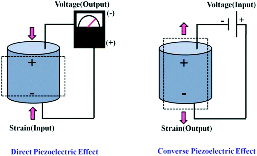 | ||
| Fig. 7 Schematic diagram of the positive piezoelectric effect and the inverse piezoelectric effect.130 | ||
The piezoelectric coefficient is one of the important parameters to characterize piezoelectric properties of materials. Improving the piezoelectric coefficient is of great practical significance for reducing the driving voltage or improving the sensitivity and accuracy of the MEMS device. Similar to bulk materials, ferroelectric thin film materials usually have excellent piezoelectric properties near MPB, so PbZr0.52Ti0.48O3 and PbZr0.53Ti0.47O3 thin films are the most commonly used.131 In addition to composition, the effects of crystallographic orientation, grain size, thickness and porosity on the piezoelectric properties of materials are also explored.132,133 Due to the hazard of Pb on environmental and human health, research on lead-free piezoelectric thin film materials has developed rapidly in recent years. Lead-free ferroelectric materials such as Bi0.5Na0.5TiO3, BiFeO3, and K0.5Na0.5NbO3, are considered as potential candidates for MEMS.41,134,135 In 2020, Liu et al. utilized Na vacancies to form nanopillars surrounded by out-of-phase boundaries in NaNbO3 films, resulting in a giant electromechanical response (piezoelectric coefficient d33 ∼ 1098 pm V−1).37 More details about the piezoelectric properties and MEMS application of ferroelectric materials have been nicely reviewed by Kanno, Muralt and Malic, et al.11,136–138
Except for the piezoelectric coefficient, parameters such as electromechanical coupling coefficient, mechanical quality factor, and Curie temperature are also important parameters in practical applications. At present, most of the research on piezoelectric materials focuses on improving the piezoelectric coefficient of materials, and how to achieve the synergistic optimization of various parameters is one of the key issues to be solved. In addition, the research on the temperature stability, fatigue resistance and reliability of piezoelectric thin films is still insufficient, and further in-depth and meticulous research is required.
3.3 Energy storage capacitors
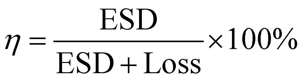
A dielectric capacitor, as an energy storage device, works through the electrostatic field generated by dielectric polarization.139 Dielectric capacitors have drawn much attention in microelectronics and power fields due to their short charge/discharge time, high endurance and long lifetime.140,141 The essential factors to achieve excellent performance energy storage devices are high energy storage density (ESD) and efficiency (η). The ESD and η of the dielectric capacitor can be estimated by the P–E curve. Fig. 8 shows the P–E hysteresis loops for dielectric materials and the calculation equation is as follows:139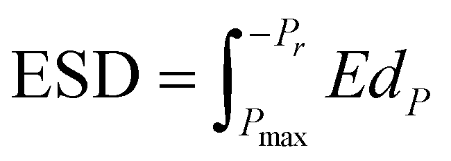
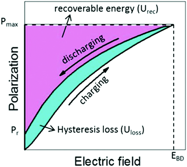 | ||
| Fig. 8 The recoverable energy storage density and loss from P–E loops of a dielectric capacitor.139 | ||
Thus, antiferroelectrics and relaxor ferroelectrics with high Ps, high breakdown electric field and low Pr are considered the most suitable materials for energy storage applications.142,143 The breakdown strength of the bulk is lower than that of thin films, which results in a smaller ESD;144 therefore, it is supposed that great energy storage properties can be obtained in the films. According to the composition, capacitors can be divided into Pb-based and lead-free capacitors.22,145 Due to the high ESD and efficiency, Pb-based capacitors have been studied intensively for decades, and many works have been published.146 The Mn-doped Pb0.91La0.09Zr0.65Ti0.35O3 relaxor ferroelectric thin films exhibit an ESD of 30.8 J cm−3 and η 68.4%.147 Nonetheless, because lead is harmful to the human body and the environment, lead-free energy storage devices have attracted more attention.140 Lead-free capacitors with energy storage performance comparable to, or even superior to, Pb-based capacitors have been fabricated.148 For instance, Pan et al. achieved high ESD (112 J cm−3) and η (80%) in BFO–BTO–STO solid solution thin films by designing a polymorphic nanodomain structure.26 A superparaelectric relaxor ferroelectric thin film (Sm-doped BFO–BTO) with ultrahigh EDS of 152 J cm−3 and η over 70% was fabricated by Pan et al.25 Since the volume and mass of the substrate is much larger than the film, so the total stored energy in ferroelectric film capacitors is much lower than that in ceramics. At present, factors hindering the commercialization of ferroelectric energy storage capacitors include: low energy density and total energy, small effective energy storage volume, poor temperature and fatigue stability, etc.
3.4 Ferroelectric photovoltaic devices
With the increasing demand for energy, it is urgent to develop and utilize clean renewable energy-solar energy. Photovoltaic technology is an important technical means to transform solar energy into electric energy. The working principle of photovoltaic devices is shown in Fig. 9. The electron–hole pairs are created in the material illuminated by sunlight, and the separation of electron–hole pairs produces a potential difference at both ends of the material.149 In order to achieve high power output, high photovoltage, photocurrent and photoelectric conversion efficiency are necessary for photovoltaic devices. The high open circuit voltage (Voc is not limited by its own band gap), good light absorption characteristics and favorable polarity structure for photogenerated carrier separation make ferroelectric photovoltaic materials have promising application prospects in solar cells.149–151 The high Pr value and low band gap (2.1–2.7 eV) make BFO thin film materials one of the most promising candidate materials in the field of photovoltaics.152–154 | ||
| Fig. 9 The working principle of ferroelectric photovoltaic devices.149 | ||
Although the photovoltaic effect mechanism of ferroelectric thin film materials has not been fully understood so far, a large number of studies have found that many factors can affect the photovoltaic effect of thin film materials, such as (i) Band gap: the narrow band gap and large absorption coefficient enable the BFO film to absorb more photons, thus producing a greater photocurrent.155,156 In 2014, Nechache et al. proposed a new strategy to tune the bandgap of double perovskite Bi2FeCrO6 thin films by regulating the cationic ordering, achieving a conversion efficiency of 8.1% in multilayer devices.157 (ii) Pr value: the larger Pr values of ferroelectric thin films can separate photogenerated carriers more effectively;31,158 (iii) Schottky barrier height: the Schottky barrier height can be modulated by changing the electrode type or polarization state, and the high Schottky barrier height facilitates the separation of photogenerated carriers;159,160 (iv) Conductivity: the separation of electrons and holes is a charge transfer process, so it is significant to improve the photoexcited charge transfer by balancing the ferroelectricity and conductivity of ferroelectric thin films,161etc. Paillard et al. published a review describing the development of ferroelectric photovoltaic materials and discussing several critical issues and parameters that require further exploration.162 Although much research on ferroelectric photovoltaic devices has been carried out, the photovoltaic efficiency of ferroelectric thin film photovoltaic devices is too low and there is still much more to explore before commercialization.
3.5 Tunable microwave devices
The tunable microwave devices fabricated by electrically tunable dielectric materials, such as tunable oscillators, phase shifters and resonators, have wide application prospects in the field of radar and communication.163,164 In the past few decades, a number of tunable microwave devices integrated with Ba1−xSrxTiO3 (BST) thin films have been fabricated, such as, a tunable band-stop resonator consisting of a high-temperature superconductor and BST bilayer163 and phase array systems with enhanced performance fabricated by microwave phase shifters.165 The key factors to the high performance of tunable microwave devices are high dielectric tunability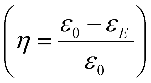 and low dielectric loss. Ferroelectric materials, especially BST thin films, with strong electrically manipulated dielectric permittivity and low dielectric loss have made them excellent alternatives for tunable microwave devices.166,167 Many investigations have been performed to improve the tunable properties of thin films. The dielectric loss of the BST thin film can be reduced by element doping (Co, Al, Mg, etc.), but the tunability is also weakened.168–170 The tunability of the SBT film can be improved by applying epitaxial strain, which induces an increase in the Curie temperature.9,54 However, due to strain relaxation, epitaxial strain cannot be maintained in the thick films required for microwave devices. In 2012, Lee et al. reported a nanocomposite ferroelectric thin film composed of BST and Sm2O3 which has an enhanced tunability (75%) and reduced dielectric loss (< 0.01), indicating great potential for application in electrically tunable microwave devices.10,66
3.6 Other application fields
In addition to the above applications, ferroelectric thin film materials can also be utilized to fabricate other devices. Such as, resistive RAM based on high/low resistance switching behavior, magnetoelectric RAM based on the magnetoelectric coupling effect, detectors based on pyroelectric effects, refrigeration devices based on the electrocaloric effect, etc.10,1714. Flexible ferroelectric devices
With the rapid development of the artificial intelligence industry and wearable electronics, higher requirements are put forward for the portability and flexibility of electronic equipment,172,173 which are difficult to meet using traditional rigid electronic devices. Hence, flexible multifunctional devices with good ductility and resilience have drawn increasing attention. Currently, nanogenerators, sensors, energy harvesting devices, and information storage devices have been fabricated by depositing polymer materials and oxide materials onto flexible substrates.174–177 Compared with polymer materials, oxide materials generally have better physical properties and superior chemical and thermal stability, which have greater advantages in the preparation and application of devices. As mentioned above, among the many functional materials, inorganic ferroelectric thin film materials have been widely used in information storage, piezoelectric devices, optoelectronics and other fields because of their excellent electrical and optical properties. Achieving the flexibility of inorganic ferroelectric thin films can further transfer the performance advantages of these materials into flexible electronic devices. Therefore, flexible inorganic ferroelectric thin film materials are very potential candidates for flexible electronic devices. Meanwhile, flexible ferroelectric devices have become a new direction for the application and development of ferroelectric thin film materials. In this section, we briefly introduce the fabrication processes and the application prospects of flexible inorganic ferroelectric thin films.4.1 Fabrication processes of flexible thin films
4.2 Application of flexible ferroelectric thin films
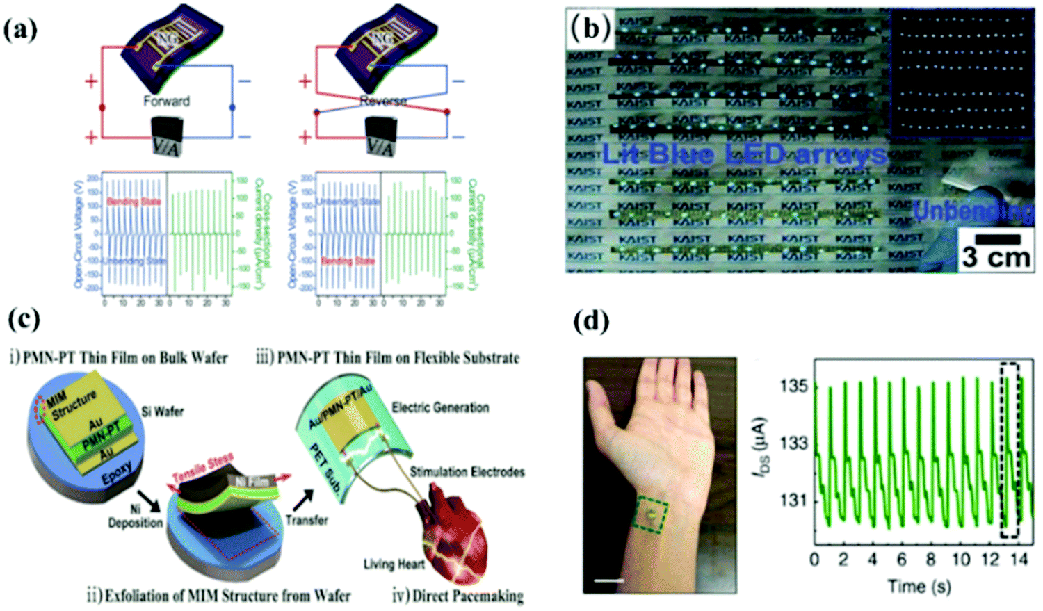 | ||
| Fig. 11 (a) The output voltage and current density of PZT thin film nanogenerators in the forward (left) and reverse (right) connections, and (b) a snapshot shows the nanogenerators can simultaneously turn on 105 blue LEDs without any external power supply.202 (c) Schematic diagrams of the fabrication process of flexible piezoelectric nanogenerators and the application of an artificial heart for a live rat.203 (d) Photograph of the sensor placed on a wrist and the accordingly measured IDS–time curves.204 | ||
The inherent piezoelectric properties of flexible ferroelectric thin films can also be used to fabricate flexile nano sensors. As shown in Fig. 11d,204 Dagdeviren et al. fabricated a PZT-based flexible sensor that can convert skin pressure to a current output via capacitance coupling, with low hysteresis, fast response time (0.1 ms) and high sensitivity (0.005 Pa). Lee et al. reported a PZT-based flexible piezoelectric acoustic nano sensor and the sensor can sensitively and efficiently convert sound energy into piezoelectric signals within the audible living noise frequency range.195 The NG can work as self-powered piezoelectric sensors.206,211 Park et al. transferred a PZT thin film onto a flexile substrate to realize a self-powered flexible sensor, and the sensor has been shown to measure radial/carotid pulse signals, respiration frequency and tracheal movements.212 Flexible nano sensors are expected to be applied in the field of wearable electronic devices and biomedical devices, such as electronic skin, health monitoring and intelligence systems, etc.172,213
Although significant progress has been made in the fabrication process of flexible inorganic ferroelectric thin films in recent years, the optimal solution between film quality, cost, and process complexity has not yet been reached, and the fabrication process needs to be improved. The thermal stability of flexible devices and the performance stability against bending need to be further studied and improved. At this stage, most of the research on flexible ferroelectric devices focuses on independent ferroelectric films or components, and there is still a lot to be done on the integration of flexible ferroelectric components and other functional components.
5. Conclusions
Ferroelectric thin film materials have been a hot topic in fundamental research and application fields for nearly one century. At present, the basic scientific research of ferroelectric thin film materials is still appealing, and some critical issues are to be thoroughly revealed, such as the size effect of perovskite ferroelectrics, the ferroelectricity origin of hafnium oxide-based materials, topological structures, strain engineering, interface effects, etc. How to derive good-performance and large-scale thin films to construct commercial devices remains to be further investigated. The preparation and research of ferroelectric thin film materials are mostly limited in the laboratory, and some fabrication methods are not suitable for large-scale commercial production. Industrial fabrication and integration process of ferroelectric thin-film devices need improvement. Moreover, there is still an urgent need to find lead-free alternatives to PZT with suitable cost and good performance.Conflicts of interest
There are no conflicts of interest to declare.Acknowledgements
This research was supported by the National Key R&D Program of China (2020YFA0406202), and the National Natural Science Foundation of China (22090042 and 21731001).References
- M. E. Lines and A. M. Glass, Principles and applications of ferroelectrics and related materials, Oxford university press, 2001 Search PubMed.
- K. Seshan, Handbook of thin film deposition techniques principles, methods, equipment and applications, CRC Press, 2nd edn, 2002 Search PubMed.
- J. E. Crowell, J. Vac. Sci. Technol., A, 2003, 21, S88–S95 CrossRef CAS.
- E. Subbarao and G. Shirane, J. Chem. Phys., 1960, 32, 1846–1851 CrossRef CAS.
- H. N. Lee, D. Hesse, N. Zakharov and U. Gosele, Science, 2002, 296, 2006–2009 CrossRef CAS PubMed.
- Y. Sakashita, T. Ono, H. Segawa, K. Tominaga and M. Okada, J. Appl. Phys., 1991, 69, 8352–8357 CrossRef CAS.
- R. J. Zeches, M. D. Rossell, J. X. Zhang, A. J. Hatt, Q. He, C.-H. Yang, A. Kumar, C. H. Wang, A. Melville, C. Adamo, G. Sheng, Y. H. Chu, J. F. Ihlefeld, R. Erni, C. Ederer, V. Gopalan, L. Q. Chen, D. G. Schlom, N. A. Spaldin, L. W. Martin and R. Remesh, Science, 2009, 326, 977–980 CrossRef CAS PubMed.
- N. Izyumskaya, Y.-I. Alivov, S.-J. Cho, H. Morkoç, H. Lee and Y.-S. Kang, Crit. Rev. Solid State Mater. Sci., 2007, 32, 111–202 CrossRef CAS.
- K. J. Choi, M. Biegalski, Y. Li, A. Sharan, J. Schubert, R. Uecker, P. Reiche, Y. Chen, X. Pan, V. Gopalan, L Chen, D Schlom and C Eom, Science, 2004, 306, 1005–1009 CrossRef CAS PubMed.
- L. W. Martin and A. M. Rappe, Nat. Rev. Mater., 2016, 2, 1–14 Search PubMed.
- I. Kanno, Jpn. J. Appl. Phys., 2018, 57, 040101 CrossRef.
- H. Takasu, J. Electroceram., 2000, 4, 327–338 CrossRef CAS.
- H. N. Lee, H. M. Christen, M. F. Chisholm, C. M. Rouleau and D. H. Lowndes, Nature, 2005, 433, 395–399 CrossRef CAS PubMed.
- M. Dawber, N. Stucki, C. Lichtensteiger, S. Gariglio, P. Ghosez and J. M. Triscone, Adv. Mater., 2007, 19, 4153–4159 CrossRef CAS.
- E. Bousquet, M. Dawber, N. Stucki, C. Lichtensteiger, P. Hermet, S. Gariglio, J.-M. Triscone and P. Ghosez, Nature, 2008, 452, 732–736 CrossRef CAS PubMed.
- A. Yadav, C. Nelson, S. Hsu, Z. Hong, J. Clarkson, C. Schlepütz, A. Damodaran, P. Shafer, E. Arenholz, L. Dedon, D. Chen, A. Vishwanath, A. Minor, L. Chen, J. Scott, L. Martin and R. Ramesh, Nature, 2016, 530, 198–201 CrossRef CAS PubMed.
- S. Das, Y. Tang, Z. Hong, M. Gonçalves, M. McCarter, C. Klewe, K. Nguyen, F. Gómez-Ortiz, P. Shafer, E. Arenholz, V. Stoica, S. Hsu, B. Wang, C. Ophus, J. Liu, C. Nelson, S. Saremi, B. Prasad, A. Mei, D. Schlom, J. Íñiguez, P. García-Fernández, D Muller, L. Chen, J. Junquera, L. Martin and R. Ramesh, Nature, 2019, 568, 368–372 CrossRef CAS PubMed.
- P. Zubko, J. C. Wojdeł, M. Hadjimichael, S. Fernandez-Pena, A. Sené, I. Luk’yanchuk, J.-M. Triscone and J. Íñiguez, Nature, 2016, 534, 524–528 CrossRef CAS PubMed.
- T. Böscke, J. Müller, D. Bräuhaus, U. Schröder and U. Böttger, Appl. Phys. Lett., 2011, 99, 102903 CrossRef.
- T. Mikolajick, S. Slesazeck, M. H. Park and U. Schroeder, MRS Bull., 2018, 43, 340–346 CrossRef CAS.
- F. Ali, X. Liu, D. Zhou, X. Yang, J. Xu, T. Schenk, J. Müller, U. Schroeder, F. Cao and X. Dong, J. Appl. Phys., 2017, 122, 144105 CrossRef.
- F. Ali, D. Zhou, M. Ali, H. W. Ali, M. Daaim, S. Khan, M. M. Hussain and N. Sun, ACS Appl. Electron. Mater., 2020, 2, 2301–2317 CrossRef CAS.
- M. Yang, S. Li, Y. Wang, H. Qi, K. Lin, Q. Li and X. Xing, Inorg. Chem. Front., 2021, 8, 5124–5129 RSC.
- D. Mukherjee, M. Hordagoda, D. Pesquera, D. Ghosh, J. L. Jones, P. Mukherjee and S. Witanachchi, Phys. Rev. B, 2017, 95, 174304 CrossRef.
- H. Pan, S. Lan, S. Xu, Q. Zhang, H. Yao, Y. Liu, F. Meng, E.-J. Guo, L. Gu and D. Yi, Science, 2021, 374, 100–104 CrossRef CAS PubMed.
- H. Pan, F. Li, Y. Liu, Q. Zhang, M. Wang, S. Lan, Y. Zheng, J. Ma, L. Gu and Y. Shen, Science, 2019, 365, 578–582 CrossRef CAS PubMed.
- Z. Pan, P. Wang, X. Hou, L. Yao, G. Zhang, J. Wang, J. Liu, M. Shen, Y. Zhang and S. Jiang, Adv. Energy Mater., 2020, 10, 2001536 CrossRef CAS.
- L. You, F. Zheng, L. Fang, Y. Zhou, L. Z. Tan, Z. Zhang, G. Ma, D. Schmidt, A. Rusydi and L. Wang, Sci. Adv., 2018, 4, eaat3438 CrossRef PubMed.
- Q. Zhang, J. Phys. D: Appl. Phys., 2003, 37, 98–101 CrossRef.
- T. Kijima, T. Aoyama, H. Miyazawa, Y. Hamada, K. Ohashi, M. Nakayama, E. Natori and T. Shimoda, Jpn. J. Appl. Phys., 2005, 44, 267–274 CrossRef CAS.
- L. Zhang, J. Chen, L. Fan, Z. Pan, J. Wang, K. Ibrahim, J. Tian and X. Xing, J. Alloys Compd., 2018, 742, 351–355 CrossRef CAS.
- J. K. Kim, S. S. Kim, W.-J. Kim, A. S. Bhalla and R. Guo, Appl. Phys. Lett., 2006, 88, 132901 CrossRef.
- L. Zhang, J. Chen, H. Zhao, L. Fan, Y. Rong, J. Deng, R. Yu and X. Xing, Appl. Phys. Lett., 2013, 103, 082902 CrossRef.
- Y. Wang, H. Zhao, K. Lin, J. Deng, J. Chen and X. Xing, Inorg. Chem. Front., 2018, 5, 1156–1161 RSC.
- M. Hoffmann, U. Schroeder, C. Künneth, A. Kersch, S. Starschich, U. Böttger and T. Mikolajick, Nano Energy, 2015, 18, 154–164 CrossRef CAS.
- T. Li, S. Deng, H. Liu, S. Sun, H. Li, S. Hu, S. Liu, X. Xing and J. Chen, Adv. Mater., 2021, 33, 2008316 CrossRef CAS PubMed.
- H. Liu, H. Wu, K. P. Ong, T. Yang, P. Yang, P. K. Das, X. Chi, Y. Zhang, C. Diao and W. K. A. Wong, Science, 2020, 369, 292–297 CrossRef CAS PubMed.
- L. Zhang, J. Chen, J. Cao, D. He and X. Xing, J. Mater. Chem. C, 2015, 3, 4706–4712 RSC.
- Q. Zhang and R. Whatmore, J. Phys. D: Appl. Phys., 2001, 34, 2296–2301 CrossRef CAS.
- S. B. Seshadri, M. M. Nolan, G. Tutuncu, J. S. Forrester, E. Sapper, G. Esteves, T. Granzow, P. A. Thomas, J. C. Nino and T. Rojac, Sci. Rep., 2018, 8, 1–13 Search PubMed.
- C.-J. Cheng, D. Kan, V. Anbusathaiah, I. Takeuchi and V. Nagarajan, Appl. Phys. Lett., 2010, 97, 212905 CrossRef.
- S. Fujino, M. Murakami, V. Anbusathaiah, S.-H. Lim, V. Nagarajan, C. Fennie, M. Wuttig, L. Salamanca-Riba and I. Takeuchi, Appl. Phys. Lett., 2008, 92, 202904 CrossRef.
- H. Zhao, J. Wang, L. Zhang, Y. Rong, J. Chen, K. Ibrahim and X. Xing, Dalton Trans., 2013, 42, 10358–10364 RSC.
- Y.-H. Lin, J. Yuan, S. Zhang, Y. Zhang, J. Liu, Y. Wang and C.-W. Nan, Appl. Phys. Lett., 2009, 95, 033105 CrossRef.
- Y. Wang, H. Zhao, L. Zhang, Z. Liu, J. Chen, J. Deng, J. Wang, K. Ibrahim, N. I. Ilinykh and X. Xing, Inorg. Chem. Front., 2016, 3, 1473–1479 RSC.
- J. Hao, Y. Zhang and X. Wei, Angew. Chem., Int. Ed., 2011, 50, 6876–6880 CrossRef CAS PubMed.
- G. Bai, W. Jie, Z. Yang and J. Hao, J. Appl. Phys., 2015, 118, 183110 CrossRef.
- I. Ponomareva and L. Bellaiche, Phys. Rev. Lett., 2008, 101, 197602 CrossRef CAS PubMed.
- Y. Wang, H. Zhao, L. Zhang, J. Chen and X. Xing, Phys. Chem. Chem. Phys., 2017, 19, 17493–17515 RSC.
- W. Merz, Phys. Rev., 1950, 78, 52–54 CrossRef CAS.
- G. Samara, Phys. Rev., 1966, 151, 378–386 CrossRef CAS.
- A. Goswami and L. Cross, Phys. Rev., 1968, 171, 549–550 CrossRef CAS.
- A. A. J. P. T. R. S. L. Griffith, Philos. Trans. R. Soc., A, 1920, 221, 163–198 Search PubMed.
- D. G. Schlom, L.-Q. Chen, C.-B. Eom, K. M. Rabe, S. K. Streiffer and J.-M. Triscone, Annu. Rev. Mater. Sci., 2007, 37, 589–626 CrossRef CAS.
- A. R. Damodaran, J. C. Agar, S. Pandya, Z. Chen, L. Dedon, R. Xu, B. Apgar, S. Saremi and L. W. Martin, J. Phys.: Condens. Matter, 2016, 28, 263001 CrossRef PubMed.
- J. Hwang, Z. Feng, N. Charles, X. R. Wang, D. Lee, K. A. Stoerzinger, S. Muy, R. R. Rao, D. Lee and R. Jacobs, Mater. Today, 2019, 31, 100–118 CrossRef CAS.
- C. Ederer and N. A. Spaldin, Phys. Rev. Lett., 2005, 95, 257601 CrossRef PubMed.
- J. Haeni, P. Irvin, W. Chang, R. Uecker, P. Reiche, Y. Li, S. Choudhury, W. Tian, M. Hawley and B. Craigo, Nature, 2004, 430, 758–761 CrossRef CAS PubMed.
- Y. Wei, P. Nukala, M. Salverda, S. Matzen, H. J. Zhao, J. Momand, A. S. Everhardt, G. Agnus, G. R. Blake and P. Lecoeur, Nat. Mater., 2018, 17, 1095–1100 CrossRef CAS PubMed.
- H. W. Jang, S. H. Baek, D. Ortiz, C. M. Folkman, R. R. Das, Y. H. Chu, P. Shafer, J. X. Zhang, S. Choudhury, V. Vaithyanathan, Y. B. Chen, D. A. Felker, M. D. bIEgalski, M. S. Rzchowski, X. Q. Pan, D. G. Schlom, L. Q. chen, R. Remesh and C. B. Eom, Phys. Rev. Lett., 2008, 101, 107602 CrossRef CAS PubMed.
- J. Wang, J. Neaton, H. Zheng, V. Nagarajan, S. Ogale, B. Liu, D. Viehland, V. Vaithyanathan, D. Schlom and U. Waghmare, Science, 2003, 299, 1719–1722 CrossRef CAS PubMed.
- J. Zhang, Q. He, M. Trassin, W. Luo, D. Yi, M. D. Rossell, P. Yu, L. You, C. H. Wang and C. Kuo, Phys. Rev. Lett., 2011, 107, 147602 CrossRef CAS PubMed.
- J. Zhang, B. Xiang, Q. He, J. Seidel, R. Zeches, P. Yu, S. Yang, C. Wang, Y. Chu and L. Martin, Nat. Nanotechnol., 2011, 6, 98–102 CrossRef CAS PubMed.
- Y. Liu, J. Wei, X. Lou, L. Bellaiche, J. F. Scott and B. Dkhil, Appl. Phys. Lett., 2015, 106, 032901 CrossRef.
- S. A. Harrington, J. Zhai, S. Denev, V. Gopalan, H. Wang, Z. Bi, S. A. Redfern, S.-H. Baek, C. W. Bark, C.-B. Eom, Q. Jia, M. E. Vickers and J. L. MacManus-Driscoll, Nat. Nanotechnol., 2011, 6, 491–495 CrossRef CAS PubMed.
- O. Lee, S. A. Harrington, A. Kursumovic, E. Defay, H. Wang, Z. Bi, C.-F. Tsai, L. Yan, Q. Jia and J. L. MacManus-Driscoll, Nano Lett., 2012, 12, 4311–4317 CrossRef CAS PubMed.
- J. L. MacManus-Driscoll, P. Zerrer, H. Wang, H. Yang, J. Yoon, A. Fouchet, R. Yu, M. G. Blamire and Q. Jia, Nat. Mater., 2008, 7, 314–320 CrossRef CAS PubMed.
- A. Kursumovic, E. Defay, O. J. Lee, C. F. Tsai, Z. Bi, H. Wang and J. L. MacManus-Driscoll, Adv. Funct. Mater., 2013, 23, 5881–5886 CrossRef CAS.
- E. Enriquez, Q. Li, P. Bowlan, P. Lu, B. Zhang, L. Li, H. Wang, A. J. Taylor, D. Yarotski and R. P. Prasankumar, Nanoscale, 2020, 12, 18193–18199 RSC.
- A. L. Sangle, O. J. Lee, A. Kursumovic, W. Zhang, A. Chen, H. Wang and J. L. MacManus-Driscoll, Nanoscale, 2018, 10, 3460–3468 RSC.
- C.-W. Nan, G. Liu, Y. Lin and H. Chen, Phys. Rev. Lett., 2005, 94, 197203 CrossRef PubMed.
- H. Zheng, J. Wang, S. Lofland, Z. Ma, L. Mohaddes-Ardabili, T. Zhao, L. Salamanca-Riba, S. Shinde, S. Ogale, F. Bai, D. Viehland, Y. Jia, D. G. Schlom, M. Wuttig, A. Roytburd and R. Remesh, Science, 2004, 303, 661–663 CrossRef CAS PubMed.
- N. M. Aimon, D. H. Kim, X. Sun and C. Ross, ACS Appl. Mater. Interfaces, 2015, 7, 2263–2268 CrossRef CAS PubMed.
- S. M. Stratulat, X. Lu, A. Morelli, D. Hesse, W. Erfurth and M. Alexe, Nano Lett., 2013, 13, 3884–3889 CrossRef CAS PubMed.
- L. Zhang, J. Chen, L. Fan, O. Diéguez, J. Cao, Z. Pan, Y. Wang, J. Wang, M. Kim, S. Deng, J. Wang, H. Wang, J. Deng, R. Yu, J. Scott and X. Xing, Science, 2018, 361, 494–497 CrossRef CAS PubMed.
- S. Mabud and A. Glazer, J. Appl. Crystallogr., 1979, 12, 49–53 CrossRef CAS.
- Y. Wang, L. Zhang, J. Wang, Q. Li, H. Wang, L. Gu, J. Chen, J. Deng, K. Lin, L. Huang and X. Xing, J. Am. Chem. Soc., 2021, 143, 6491–6497 CrossRef CAS PubMed.
- L. Zhang, D. Zheng, L. Fan, J. Wang, M. Kim, J. Wang, H. Wang, X. Xing, J. Tian and J. Chen, Nano Lett., 2019, 20, 881–886 CrossRef PubMed.
- D. Lu, D. J. Baek, S. S. Hong, L. F. Kourkoutis, Y. Hikita and H. Y. Hwang, Nat. Mater., 2016, 15, 1255–1260 CrossRef CAS PubMed.
- S. S. Hong, J. H. Yu, D. Lu, A. F. Marshall, Y. Hikita, Y. Cui and H. Y. Hwang, Sci. Adv., 2017, 3, eaao5173 CrossRef PubMed.
- G. Dong, S. Li, M. Yao, Z. Zhou, Y.-Q. Zhang, X. Han, Z. Luo, J. Yao, B. Peng, Z. Hu, H. Huang, T. Jia, J. Li, W. Ren, Z. Ye, X. Ding, J. Sun, C. Nan, L. Chen, J. Li and M. Liu, Science, 2019, 366, 475–479 CrossRef CAS PubMed.
- D. Ji, S. Cai, T. R. Paudel, H. Sun, C. Zhang, L. Han, Y. Wei, Y. Zang, M. Gu, Y. Zhang, W. Gao, H. Huyan, W. Guo, D. Wu, Z. Gu, E. Tsymbal, P. Wang, Y. Nie and X. Pan, Nature, 2019, 570, 87–90 CrossRef CAS PubMed.
- H. Béa, B. Dupé, S. Fusil, R. Mattana, E. Jacquet, B. Warot-Fonrose, F. Wilhelm, A. Rogalev, S. Petit and V. Cros, Phys. Rev. Lett., 2009, 102, 217603 CrossRef PubMed.
- T. Li, Y. Zhu, S. B. Desu, C. H. Peng and M. Nagata, Appl. Phys. Lett., 1996, 68, 616–618 CrossRef CAS.
- L. Zhang, J. Chen, H. Zhao, L. Fan, Y. Rong, J. Deng, R. Yu and X. Xing, Dalton Trans., 2013, 42, 585–590 RSC.
- M. Calzada, M. Martin, P. Ramos, J. Mendiola, R. Sirera, M. Da Silva and J. Soares, J. Phys. Chem. Solids, 1997, 58, 1033–1039 CrossRef CAS.
- Y. Wang, W. Chen, B. Wang and Y. Zheng, Materials, 2014, 7, 6377–6485 CrossRef PubMed.
- J. F. Scott and C. A. Paz de Araujo, Science, 1989, 246, 1400–1405 CrossRef CAS PubMed.
- Y. Arimoto and H. Ishiwara, MRS Bull., 2004, 29, 823–828 CrossRef CAS.
- C. De Araujo, J. Cuchiaro, L. McMillan, M. Scott and J. Scott, Nature, 1995, 374, 627–629 CrossRef CAS.
- C.-H. Yang, S.-S. Park and S.-G. Yoon, Integr. Ferroelectr., 1997, 18, 377–387 CrossRef CAS.
- L. Goux, G. Russo, N. Menou, J. G. Lisoni, M. Schwitters, V. Paraschiv, D. Maes, C. Artoni, G. Corallo, L. Haspeslagh, D. Wouters, R. Zambrano and C. Muller, IEEE Trans. Electron Devices, 2005, 52, 447–453 CrossRef CAS.
- J. Ze, R. Tian-Ling, Z. Zhi-Gang, L. Tian-Zhi, W. Xin-Yi, X. Dan and L. Li-Tian, Chin. Phys. Lett., 2006, 23, 1943–1946 CrossRef.
- S. Majumder, D. Agrawal, Y. Mohapatra and R. Katiyar, Integr. Ferroelectr., 2000, 29, 63–74 CrossRef.
- R. Moazzami, C. Hu and W. H. Shepherd, IEEE Trans. Electron Devices, 1992, 39, 2044–2049 CrossRef CAS.
- X. Meng, J. Sun, J. Yu, G. Wang, S. Guo and J. Chu, Appl. Phys. A: Mater. Sci. Process., 2001, 73, 323–325 CrossRef CAS.
- B. Nagaraj, S. Aggarwal and R. Ramesh, J. Appl. Phys., 2001, 90, 375–382 CrossRef CAS.
- H. P. McAdams, R. Acklin, T. Blake, X.-H. Du, J. Eliason, J. Fong, W. F. Kraus, D. Liu, S. Madan, T. Moise, S. Natarajan, N. Qian, Y. Qiu, K. Remack, J. Rodriguez, J. Roscher, A. Seshadri and S. Summerfelt, IEEE J. Solid-State Circuits, 2004, 39, 667–677 CrossRef.
- J. Rodriguez, K. Remack, J. Gertas, K. Boku, K. Udayakumar, S. Summerfelt, G. Shinn, A. Haider, S. Madan and H. McAdams, in Reliability characterization of a Ferroelectric Random Access Memory embedded within 130 nm CMOS, 2008 17th IEEE International Symposium on the Applications of Ferroelectrics, 2008 Search PubMed.
- V. K. M. V. M. Kondo, V. S. K. Singh and V. H. Ishiwara, Fujitsu Sci. Tech. J., 2007, 43, 502–507 Search PubMed.
- C. Huang, Z. Liao, M. Li, C. Guan, F. Jin, M. Ye, X. Zeng, T. Zhang, Z. Chen and Y. Qi, Adv. Sci., 2021, 8, 2003582 CrossRef CAS PubMed.
- N. Nagel, R. Bruchhaus, K. Hornik, U. Egger, H. Zhuang, H.-O. Joachim, T. Rohr, G. Beitel, T. Ozaki and I. Kunishima, in New highly scalable 3 dimensional chain FeRAM cell with vertical capacitor, Digest of Technical Papers, 2004 Symposium on VLSI Technology, 2004 Search PubMed.
- P. Polakowski, S. Riedel, W. Weinreich, M. Rudolf, J. Sundqvist, K. Seidel and J. Muller, in Ferroelectric deep trench capacitors based on Al: HfO2 for 3D nonvolatile memory applications, 2004 IEEE 6th International Memory Workshop (IMW), 2014 Search PubMed.
- C.-P. Yeh, M. Lisker, B. Kalkofen and E. P. Burte, AIP Adv., 2016, 6, 035128 CrossRef.
- T. Francois, L. Grenouillet, J. Coignus, P. Blaise, C. Carabasse, N. Vaxelaire, T. Magis, F. Aussenac, V. Loup and C. Pellissier, in Demonstration of BEOL-compatible ferroelectric Hf 0.5 Zr 0.5 O 2 scaled FeRAM co-integrated with 130 nm CMOS for embedded NVM applications, 2019 IEEE International Electron Devices Meeting (IEDM), 2019 Search PubMed.
- M. H. Park, Y. H. Lee, T. Mikolajick, U. Schroeder and C. S. Hwang, MRS Commun., 2018, 8, 795–808 CrossRef CAS.
- S. Mueller, J. Muller, U. Schroeder and T. Mikolajick, IEEE Trans. Device Mater. Reliab., 2012, 13, 93–97 Search PubMed.
- S.-Y. Wu, IEEE Trans. Electron Devices, 1974, 21, 499–504 Search PubMed.
- T.-Q. Shao, T.-L. Ren, C.-G. Wei, X.-N. Wang, C.-X. Li, J.-S. Liu, L.-T. Liu, J. Zhu and Z.-J. Li, Integr. Ferroelectr., 2003, 57, 1241–1248 CrossRef CAS.
- M. Takahashi, W. Zhang and S. Sakai, in High-endurance ferroelectric NOR flash memory using (Ca, Sr) Bi2Ta2O9 FeFETs, 2018 IEEE International Memory Workshop (IMW), 2018 Search PubMed.
- X. Chai, J. Jiang, Q. Zhang, X. Hou, F. Meng, J. Wang, L. Gu, D. W. Zhang and A. Q. Jiang, Nat. Commun., 2020, 11, 1–9 CrossRef PubMed.
- M. Si, P.-Y. Liao, G. Qiu, Y. Duan and P. D. Ye, ACS Nano, 2018, 12, 6700–6705 CrossRef CAS PubMed.
- J. Hoffman, X. Pan, J. W. Reiner, F. J. Walker, J. Han, C. H. Ahn and T. Ma, Adv. Mater., 2010, 22, 2957–2961 CrossRef CAS PubMed.
- X. Pan and T. Ma, Appl. Phys. Lett., 2011, 99, 013505 CrossRef.
- H.-T. Lue, C.-J. Wu and T.-Y. Tseng, IEEE Trans. Electron Devices, 2002, 49, 1790–1798 CrossRef.
- D. Xie, Y. Luo, X. Han, T. Ren and L. Liu, J. Appl. Phys., 2009, 106, 114117 CrossRef.
- X. Lu and H. Ishiwara, J. Appl. Phys., 2009, 105, 061626 CrossRef.
- M. Si, A. K. Saha, S. Gao, G. Qiu, J. Qin, Y. Duan, J. Jian, C. Niu, H. Wang and W. Wu, Nat. Electron., 2019, 2, 580–586 CrossRef CAS.
- M. Takahashi and S. Sakai, Jpn. J. Appl. Phys., 2005, 44, L800–L802 CrossRef CAS.
- E. Tokumitsu, G. Fujii and H. Ishiwara, Jpn. J. Appl. Phys., 2000, 39, 2125–2130 CrossRef CAS.
- U. Schroeder, S. Slesazeck and T. Mikolajick, in Ferroelectric-Gate Field Effect Transistor Memories, Springer, 2016, pp. 57–72 Search PubMed.
- T. Böscke, J. Müller, D. Bräuhaus, U. Schröder and U. Böttger, in Ferroelectricity in hafnium oxide: CMOS compatible ferroelectric field effect transistors, 2011 International electron devices meeting, 2011 Search PubMed.
- M. Trentzsch, S. Flachowsky, R. Richter, J. Paul, B. Reimer, D. Utess, S. Jansen, H. Mulaosmanovic, S. Müller and S. Slesazeck, in A 28 nm HKMG super low power embedded NVM technology based on ferroelectric FETs, 2016 IEEE International Electron Devices Meeting (IEDM), 2016 Search PubMed.
- S. Dünkel, M. Trentzsch, R. Richter, P. Moll, C. Fuchs, O. Gehring, M. Majer, S. Wittek, B. Müller and T. Melde, in A FeFET based super-low-power ultra-fast embedded NVM technology for 22 nm FDSOI and beyond, 2017 IEEE International Electron Devices Meeting (IEDM), 2017 Search PubMed.
- S. S. Cheema, D. Kwon, N. Shanker, R. Dos Reis, S.-L. Hsu, J. Xiao, H. Zhang, R. Wagner, A. Datar, M. R. McCarter, C. R. Serrao, A. K. Yadav, G. Karbasian, C.-H. Hsu, A. J. Tan, L.-c Wang, V. Thakare, X. Zhang, A. Mehta, E. karapetrova, R. V. Chopdekar, P. Shafer, E. Arenholz, C. Hu, R. Proksch, R. Ramesh, J. Ciston and S. Salahuddin, Nature, 2020, 580, 478–482 CrossRef CAS PubMed.
- J. C. Wong and S. Salahuddin, Proc. IEEE, 2018, 107, 49–62 Search PubMed.
- A. I. Khan, A. Keshavarzi and S. Datta, Nat. Electron., 2020, 3, 588–597 CrossRef.
- Z. D. Luo, M. M. Yang, Y. Liu and M. Alexe, Adv. Mater., 2021, 33, 2005620 CrossRef CAS PubMed.
- H. Mulaosmanovic, E. T. Breyer, T. Mikolajick and S. Slesazeck, Nat. Electron., 2020, 3, 391–397 CrossRef.
- S. Mishra, L. Unnikrishnan, S. K. Nayak and S. Mohanty, Macromol. Mater. Eng., 2019, 304, 1800463 CrossRef.
- P. Muralt, R. G. Polcawich and S. Trolier-McKinstry, MRS Bull., 2009, 34, 658–664 CrossRef CAS.
- N. Ledermann, P. Muralt, J. Baborowski, S. Gentil, K. Mukati, M. Cantoni, A. Seifert and N. Setter, Sens. Actuators, A, 2003, 105, 162–170 CrossRef CAS.
- A. Matavž, A. Bradeško, T. Rojac, B. Malič and V. Bobnar, Appl. Mater. Today, 2019, 16, 83–89 CrossRef.
- Y. H. Jeon, E. A. Patterson, D. P. Cann, P. Mardilovich, W. Stickel and B. Gibbons, J. Am. Ceram. Soc., 2013, 96, 2172–2178 CrossRef CAS.
- S. S. Won, J. Lee, V. Venugopal, D.-J. Kim, J. Lee, I. W. Kim, A. I. Kingon and S.-H. Kim, Appl. Phys. Lett., 2016, 108, 232908 CrossRef.
- P. Muralt, J. Micromech. Microeng., 2000, 10, 136–146 CrossRef CAS.
- S. Trolier-McKinstry and P. Muralt, J. Electroceram., 2004, 12, 7–17 CrossRef CAS.
- S. Zhang, B. Malič, J.-F. Li and J. J. J. o M. R. Rödel, J. Mater. Res., 2021, 36, 985–995 CrossRef CAS.
- H. Palneedi, M. Peddigari, G. T. Hwang, D. Y. Jeong and J. Ryu, Adv. Funct. Mater., 2018, 28, 1803665 CrossRef.
- H. Zhang, T. Wei, Q. Zhang, W. Ma, P. Fan, D. Salamon, S.-T. Zhang, B. Nan, H. Tan and Z.-G. Ye, J. Mater. Chem. C, 2020, 8, 16648–16667 RSC.
- B. Chu, X. Zhou, K. Ren, B. Neese, M. Lin, Q. Wang, F. Bauer and Q. Zhang, Science, 2006, 313, 334–336 CrossRef CAS PubMed.
- M. D. Nguyen, C. T. Nguyen, H. N. Vu and G. Rijnders, J. Eur. Ceram. Soc., 2018, 38, 95–103 CrossRef.
- C. W. Ahn, G. Amarsanaa, S. S. Won, S. A. Chae, D. S. Lee and I. W. Kim, ACS Appl. Mater. Interfaces, 2015, 7, 26381–26386 CrossRef CAS PubMed.
- Y. Tian, L. Jin, H. Zhang, Z. Xu, X. Wei, E. Politova, S. Y. Stefanovich, N. V. Tarakina, I. Abrahams and H. Yan, J. Mater. Chem. A, 2016, 4, 17279–17287 RSC.
- S. K. Thatikonda, W. Huang, X. Du, C. Yao, Y. Ke, J. Wu, N. Qin and D. Bao, Ceram. Int., 2019, 45, 23586–23591 CrossRef CAS.
- M. Ye, Q. Sun, X. Chen, Z. Jiang and F. Wang, J. Am. Ceram. Soc., 2011, 94, 3234–3236 CrossRef CAS.
- Y. Liu, X. Hao and S. An, J. Appl. Phys., 2013, 114, 174102 CrossRef.
- Z. Pan, J. Ding, X. Hou, S. Shi, L. Yao, J. Liu, P. Li, J. Chen, J. Zhai and H. Pan, J. Mater. Chem. A, 2021, 9, 9281–9290 RSC.
- Y. Yuan, Z. Xiao, B. Yang and J. Huang, J. Mater. Chem. A, 2014, 2, 6027–6041 RSC.
- S. Y. Yang, J. Seidel, S. J. Byrnes, P. Shafer, C.-H. Yang, M. D. Rossell, P. Yu, Y.-H. Chu, J. Scott, J. W. Ager, L. W. Martin and R. Remesh, Nat. Nanotechnol., 2010, 5, 143–147 CrossRef CAS PubMed.
- Y. Liu, S. Wang, Z. Chen and L. Xiao, Sci. China Mater., 2016, 59, 851–866 CrossRef CAS.
- K. H. Tan, Y.-W. Chen, C. N. Van, H. Wang, J.-W. Chen, F. S. Lim, K.-H. Chew, Q. Zhan, C.-L. Wu and S.-P. Chai, ACS Appl. Mater. Interfaces, 2018, 11, 1655–1664 CrossRef PubMed.
- W. Ji, K. Yao and Y. C. Liang, Adv. Mater., 2010, 22, 1763–1766 CrossRef CAS PubMed.
- M. M. Seyfouri, D. J. C. R. i S. S. Wang and M. Sciences, Crit. Rev. Solid State Mater. Sci., 2021, 46, 83–108 CrossRef CAS.
- J. Zhang, P. Ma, T. Shi and X. Shao, Thin Solid Films, 2020, 698, 137852 CrossRef CAS.
- J. Wang, L. Luo, C. Han, R. Yun, X. Tang, Y. Zhu, Z. Nie, W. Zhao and Z. Feng, Materials, 2019, 12, 1444 CrossRef CAS PubMed.
- R. Nechache, C. Harnagea, S. Li, L. Cardenas, W. Huang, J. Chakrabartty and F. Rosei, Nat. Photonics, 2015, 9, 61–67 CrossRef CAS.
- W. Pei, J. Chen, D. You, Q. Zhang, M. Li, Y. Lu, Z. Fu and Y. He, Appl. Surf. Sci., 2020, 530, 147194 CrossRef CAS.
- Y. Ukai, S. Yamazaki, T. Kawae and A. Morimoto, Jpn. J. Appl. Phys., 2012, 51, 09LE10 CrossRef.
- S. Sharma, M. Tomar and V. Gupta, Vacuum, 2018, 158, 117–120 CrossRef CAS.
- Z. Fan, W. Ji, T. Li, J. Xiao, P. Yang, K. P. Ong, K. Zeng, K. Yao and J. Wang, Acta Mater., 2015, 88, 83–90 CrossRef CAS.
- C. Paillard, X. Bai, I. C. Infante, M. Guennou, G. Geneste, M. Alexe, J. Kreisel and B. Dkhil, Adv. Mater., 2016, 28, 5153–5168 CrossRef CAS PubMed.
- H. Su, M. Lancaster, F. Huang and F. Wellhofer, Microw. Opt. Technol. Lett., 2000, 24, 155–158 CrossRef.
- S. S. Gevorgian and E. L. Kollberg, IEEE Trans. Microwave Theory Tech., 2001, 49, 2117–2124 CrossRef CAS.
- B. Acikel, T. R. Taylor, P. J. Hansen, J. S. Speck and R. A. York, IEEE Microw. Wirel. Compon. Lett., 2002, 12, 237–239 Search PubMed.
- J. Pond, S. Kirchoefer, W. Chang, J. Horwitz and D. Chrisey, Integr. Ferroelectr., 1998, 22, 317–328 CrossRef CAS.
- J. Xu, W. Menesklou and E. Ivers-Tiffee, J. Eur. Ceram. Soc., 2004, 24, 1735–1739 CrossRef CAS.
- P. Joshi and M. Cole, Appl. Phys. Lett., 2000, 77, 289–291 CrossRef CAS.
- L. Xiao, K.-L. Choy and I. Harrison, Surf. Coat. Technol., 2011, 205, 2989–2993 CrossRef CAS.
- K. Chong, L. Kong, L. Chen, L. Yan, C. Tan, T. Yang, C. Ong and T. Osipowicz, J. Appl. Phys., 2004, 95, 1416–1419 CrossRef CAS.
- Z. J. Wang and Y. Bai, Small, 2019, 15, 1805088 CrossRef PubMed.
- S. Xu, Y. Zhang, L. Jia, K. E. Mathewson, K.-I. Jang, J. Kim, H. Fu, X. Huang, P. Chava, R. Wang, S. Bhole, L. Wang, Y. J. Na, Y. Guan, M. Flavin, Z. Han, Y. Huang and J. A. Rogers, Science, 2014, 344, 70–74 CrossRef CAS PubMed.
- Y. H. Jung, S. K. Hong, H. S. Wang, J. H. Han, T. X. Pham, H. Park, J. Kim, S. Kang, C. D. Yoo and K. J. Lee, Adv. Mater., 2020, 32, 1904020 CrossRef CAS PubMed.
- M. Yao, Y. Cheng, Z. Zhou and M. Liu, J. Mater. Chem. C, 2020, 8, 14–27 RSC.
- Z. M. Tsikriteas, J. I. Roscow, C. R. Bowen and H. Khanbareh, iScience, 2021, 24, 101987 CrossRef CAS PubMed.
- X. Zhang, J. Jiang, Z. Shen, Z. Dan, M. Li, Y. Lin, C. W. Nan, L. Chen and Y. Shen, Adv. Mater., 2018, 30, 1707269 CrossRef PubMed.
- X. Han, X. Chen, X. Tang, Y. L. Chen, J. H. Liu and Q. D. Shen, Adv. Funct. Mater., 2016, 26, 3640–3648 CrossRef CAS.
- H. Palneedi, H. G. Yeo, G.-T. Hwang, V. Annapureddy, J.-W. Kim, J.-J. Choi, S. Trolier-McKinstry and J. Ryu, APL Mater., 2017, 5, 096111 CrossRef.
- M. Tomczyk, I. Bretos, R. Jiménez, A. Mahajan, E. V. Ramana, M. L. Calzada and P. M. Vilarinho, J. Mater. Chem. C, 2017, 5, 12529–12537 RSC.
- S. S. Won, H. Seo, M. Kawahara, S. Glinsek, J. Lee, Y. Kim, C. K. Jeong, A. I. Kingon and S.-H. Kim, Nano Energy, 2019, 55, 182–192 CrossRef CAS.
- W. Liang, Z. Li, Z. Bi, T. Nan, H. Du, C. Nan, C. Chen, Q. Jia and Y. Lin, J. Mater. Chem. C, 2014, 2, 708–714 RSC.
- Y. J. Ko, D. Y. Kim, S. S. Won, C. W. Ahn, I. W. Kim, A. I. Kingon, S.-H. Kim, J.-H. Ko and J. H. Jung, ACS Appl. Mater. Interfaces, 2016, 8, 6504–6511 CrossRef CAS PubMed.
- I. Bretos, R. Jiménez, A. Wu, A. I. Kingon, P. M. Vilarinho and M. L. Calzada, Adv. Mater., 2014, 26, 1405–1409 CrossRef CAS PubMed.
- I. Bretos, R. Jiménez, J. Ricote, R. Sirera and M. L. Calzada, Adv. Funct. Mater., 2020, 30, 2001897 CrossRef CAS.
- Í. Bretos, R. Jiménez, J. Ricote and M. L. Calzada, IEEE Trans. Ultrason. Eng., 2020, 67, 1967–1979 Search PubMed.
- A. Koma and K. Yoshimura, Surf. Sci., 1986, 174, 556–560 CrossRef CAS.
- J. Jiang, Y. Bitla, C.-W. Huang, T. H. Do, H.-J. Liu, Y.-H. Hsieh, C.-H. Ma, C.-Y. Jang, Y.-H. Lai and P.-W. Chiu, Sci. Adv., 2017, 3, e1700121 CrossRef PubMed.
- C. Yang, Y. Han, J. Qian and Z. Cheng, Adv. Electron. Mater., 2019, 5, 1900443 CrossRef CAS.
- Y. Yang, G. Yuan, Z. Yan, Y. Wang, X. Lu and J. M. Liu, Adv. Mater., 2017, 29, 1700425 CrossRef PubMed.
- Y. Bitla and Y.-H. Chu, FlatChem, 2017, 3, 26–42 CrossRef CAS.
- S. R. Bakaul, C. R. Serrao, M. Lee, C. W. Yeung, A. Sarker, S.-L. Hsu, A. K. Yadav, L. Dedon, L. You and A. I. Khan, Nat. Commun., 2016, 7, 1–5 Search PubMed.
- L. Han, Y. Fang, Y. Zhao, Y. Zang, Z. Gu, Y. Nie and X. Pan, Adv. Mater. Interfaces, 2020, 7, 1901604 CrossRef CAS.
- S. Kim, J. H. Son, S. H. Lee, B. K. You, K. I. Park, H. K. Lee, M. Byun and K. J. Lee, Adv. Mater., 2014, 26, 7480–7487 CrossRef CAS PubMed.
- W. Wong, T. Sands and N. Cheung, Appl. Phys. Lett., 1998, 72, 599–601 CrossRef CAS.
- H. S. Lee, J. Chung, G. T. Hwang, C. K. Jeong, Y. Jung, J. H. Kwak, H. Kang, M. Byun, W. D. Kim and S. Hur, Adv. Funct. Mater., 2014, 24, 6914–6921 CrossRef CAS.
- C. K. Jeong, K.-I. Park, J. H. Son, G.-T. Hwang, S. H. Lee, D. Y. Park, H. E. Lee, H. K. Lee, M. Byun and K. J. Lee, Energy Environ. Sci., 2014, 7, 4035–4043 RSC.
- M. T. Ghoneim and M. M. Hussain, Electronics, 2015, 4, 424–479 CrossRef CAS.
- W. Xiao, C. Liu, Y. Peng, S. Zheng, Q. Feng, C. Zhang, J. Zhang, Y. Hao, M. Liao and Y. Zhou, ACS Appl. Electron. Mater., 2019, 1, 919–927 CrossRef CAS.
- S. R. Bakaul, C. R. Serrao, O. Lee, Z. Lu, A. Yadav, C. Carraro, R. Maboudian, R. Ramesh and S. Salahuddin, Adv. Mater., 2017, 29, 1605699 CrossRef PubMed.
- H. Yu, C. C. Chung, N. Shewmon, S. Ho, J. H. Carpenter, R. Larrabee, T. Sun, J. L. Jones, H. Ade and B. T. O'Connor, Adv. Funct. Mater., 2017, 27, 1700461 CrossRef.
- M.-F. Tsai, J. Jiang, P.-W. Shao, Y.-H. Lai, J.-W. Chen, S.-Z. Ho, Y.-C. Chen, D.-P. Tsai and Y.-H. Chu, ACS Appl. Mater. Interfaces, 2019, 11, 25882–25890 CrossRef CAS PubMed.
- G. T. Hwang, V. Annapureddy, J. H. Han, D. J. Joe, C. Baek, D. Y. Park, D. H. Kim, J. H. Park, C. K. Jeong and K. I. Park, Adv. Energy Mater., 2016, 6, 1600237 CrossRef.
- Y. Hu and Z. L. Wang, Nano Energy, 2015, 14, 3–14 CrossRef CAS.
- X. Wang, J. Song, J. Liu and Z. L. Wang, Science, 2007, 316, 102–105 CrossRef CAS PubMed.
- F. R. Fan, W. Tang and Z. L. Wang, Adv. Mater., 2016, 28, 4283–4305 CrossRef CAS PubMed.
- C. Dagdeviren, Y. Su, P. Joe, R. Yona, Y. Liu, Y.-S. Kim, Y. Huang, A. R. Damadoran, J. Xia and L. W. Martin, Nat. Commun., 2014, 5, 1–10 Search PubMed.
- K.-I. Park, S. Xu, Y. Liu, G.-T. Hwang, S.-J. L. Kang, Z. L. Wang and K. J. Lee, Nano Lett., 2010, 10, 4939–4943 CrossRef CAS PubMed.
- K. I. Park, J. H. Son, G. T. Hwang, C. K. Jeong, J. Ryu, M. Koo, I. Choi, S. H. Lee, M. Byun and Z. L. Wang, Adv. Mater., 2014, 26, 2514–2520 CrossRef CAS PubMed.
- S. Liu, Z. Zhang, Y. Shan, Y. Hong, F. Farooqui, F. S. Lam, W.-H. Liao, Z. Wang and Z. Yang, Mater. Chem. Front., 2021, 5, 4682–4689 RSC.
- G. T. Hwang, H. Park, J. H. Lee, S. Oh, K. I. Park, M. Byun, H. Park, G. Ahn, C. K. Jeong and K. No, Adv. Mater., 2014, 26, 4880–4887 CrossRef CAS PubMed.
- X. Cao, Y. Xiong, J. Sun, X. Zhu, Q. Sun and Z. L. Wang, Adv. Funct. Mater., 2021, 31, 2102983 CrossRef CAS.
- D. Y. Park, D. J. Joe, D. H. Kim, H. Park, J. H. Han, C. K. Jeong, H. Park, J. G. Park, B. Joung and K. J. Lee, Adv. Mater., 2017, 29, 1702308 CrossRef PubMed.
- G. T. Hwang, M. Byun, C. K. Jeong and K. J. Lee, Adv. Healthcare Mater., 2015, 4, 646–658 CrossRef CAS PubMed.
| This journal is © The Royal Society of Chemistry 2022 |