
 Open Access Article
 This Open Access Article is licensed under a Creative Commons Attribution-Non Commercial 3.0 Unported Licence
van der Waals epitaxy of transition metal dichalcogenides via molecular beam epitaxy: looking back and moving forward
Deependra Kumar
Singh
 *a and
Govind
Gupta
*ab
*a and
Govind
Gupta
*ab
aSensor Devices & Metrology Group, CSIR-National Physical Laboratory, Dr K. S. Krishnan Road, New Delhi – 110012, India. E-mail: deependras@iisc.ac.in
bAcademy of Scientific & Innovative Research, CSIR-HRDC Campus, Ghaziabad, Uttar Pradesh – 201002, India. E-mail: govind@nplindia.org; govind.npl@nic.in
First published on 29th June 2022
Abstract
Initiated by the discovery of graphene, tremendous research advances have been witnessed in the field of two-dimensional (2D) transition metal dichalcogenides (TMDCs) in the past few years. The unique optical and electrical properties of these layered TMDCs due to their well-defined low dimensionalities make them promising building blocks for next-generation electronics. Recently, a lot of research interest has been focussed on the growth of high-quality and large-area epilayers of several TMDCs using molecular beam epitaxy (MBE), owing to their ultra-high vacuum environment. The capability to precisely control the composition, thickness, and structural phases of TMDCs by MBE makes it suitable for studying fundamental sciences, investigating technological applications, and exploring new physics, which possibly could lead to fascinating applications. In the current perspective, an overview of the basic properties of TMDCs has been discussed, followed by the recent advancements in this area of the growth of TMDC thin films by MBE. Finally, the authors’ viewpoints highlight this emerging research field's key challenges and opportunities.
1. Introduction
Over the last few decades, with the research advancements in the established and matured technology of traditional three-dimensional (3D) semiconductors such as III-nitrides, metal oxides, Si, etc.,1–8 high-performance state-of-the-art electronic devices have been successfully fabricated. However, further progress and developments in these devices are often limited due to certain drawbacks encountered in these 3D semiconductors, for instance, the low charge carrier mobility, presence of dangling bonds at the surface, low light absorption properties, etc.9,10 Hence, it becomes vital to explore alternatives that can overcome these limitations, for the development of next-generation devices. Therefore, two-dimensional (2D) layered materials have recently become a priority choice for applications in modern-day electronics.11–15 The successful experimental realization of graphene16 in 2004 led to a plethora of research in the field of ultrathin layered materials,9,17–19 and several other graphene alternatives have been recently explored for various applications.20–34 Among these, a particular class of layered materials, i.e., transition metal dichalcogenides (TMDCs), has garnered significant interest, owing to their rich physics and fascinating potential applications.35–41 TMDCs, just like graphene, can be scaled down to monolayers, although these TMDCs are three atoms thick instead of one.42 TMDC-based devices possess considerable charge carrier mobility and a semiconducting band gap, making them suitable for switching applications,25 and therefore, exhibit significant photoluminescence (PL) and intrinsic on-off current ratios as compared to graphene.43–45 Additionally, TMDCs have also shown remarkable physical properties such as high tensile strength, making them a promising constituent in advanced device technology.46However, the yield and cost are a major bottleneck in the extensive application of these layered materials. Presently, the most common and widely used technique to produce ultrathin TMDCs is exfoliation;47–53 however, it presents specific common challenges such as the growth of high-quality thin films, scaling up for wafer-scale production, etc.54,55 Therefore, considerable efforts have been made to research and optimize different production methodologies of these 2D layered TMDCs,56–59 to improve their production yield without compromising the growth quality. One promising yet less-explored method to synthesize high-quality, epitaxial, and large area thin films of 2D TMDCs is via molecular beam epitaxy (MBE) due to its several potential advantages over the other growth techniques. The growth in MBE can be highly controlled because of the use of high-purity source materials, limiting contaminations due to growth carried out in an ultrahigh vacuum environment.60–62
Many reviews exist regarding the growth and applications of TMDCs by various synthesis techniques. McDonnell et al.63 have described the current status of TMDC thin film-based research, highlighting the importance of electronic and photonic applications. Lin et al.64 have reported the recent progress in the field of thin-film synthesis and the processing techniques that exhibit excellent controllability and reliability for the substitutional doping of TMDC thin film monolayers. Walsh et al.65 have discussed the various growth modes and the advantages of van der Waals (vdW) epitaxy, along with the most significant issues regarding the growth of TMDCs and topological insulators, including defect density, grain size control, electronic transport, doping, etc. Manzeli et al.66 have examined the various synthesis methods for TMDCs along with a discussion about their properties, with specific focus on the superconductivity, charge density wave, and topological phases. Moreover, TMCD-based nanoelectronic devices have also been discussed and the strategies to improve and tailor the charge carrier properties have also been explored. However, a comprehensive analysis focussed on the recent advances and current prospects on TMDCs exclusively grown by MBE is still missing. In this perspective, we aim to provide a brief overview of MBE and the basic properties of TMDCs, following which an in-depth deliberation on the recent progress of the MBE-grown TMDCs for various applications is presented. Finally, we have discussed the unresolved issues and future perspectives for this evolving family of materials.
2. Transition metal dichalcogenides
TMDCs are represented by the formula MX2, where M is a d block metal (Mo, W, Pd, Ti, etc.), and X represents a chalcogen (S, Te, and Se), respectively. The groups IV–X in the periodic table usually belong to these transition metals, containing a different number of valence d-electrons, giving rise to different electronic properties of these elements such as metallic, superconducting, semiconducting, etc.66 TMDCs exist in a layered structure at the atomic level, consisting of one or a few monolayers.67 A representative schematic depicting the layered structure of MoS2 is shown in Fig. 1(a). TMDCs usually occur in several crystal structures due to the difference in the coordination environments of the transition metal. The two most common crystal structures of the TMDCs are the trigonal prismatic structure (2H) and the octahedral phase (1T). One can understand these structural phases in terms of the different stacking arrangements of the constituent atoms. Fig. 1(b) shows the different atomic structures of MoS2. The three atoms, i.e., chalcogen–transition metal–chalcogen, form the individual monolayers of TMDCs. The ABA stacking characterizes the 2H crystal phase, while the 1T octahedral phase corresponds to the ABC stacking sequence. Most of the TMDCs (MoS2, WS2, WSe2, MoSe2, MoTe2, etc.) are thermodynamically more stable in their 2H phase than the metastable 1T octahedral phase.67 In the 2H phase, TMDCs show semiconducting characteristics that accentuate TMDCs for potential next-generation electronic applications. The metastable or intermediate state for the 2H phase of TMDCs is the orthorhombic phase (1T′ phase). For WTe2, the most stable crystal phase is the 1T′ phase at room temperature.67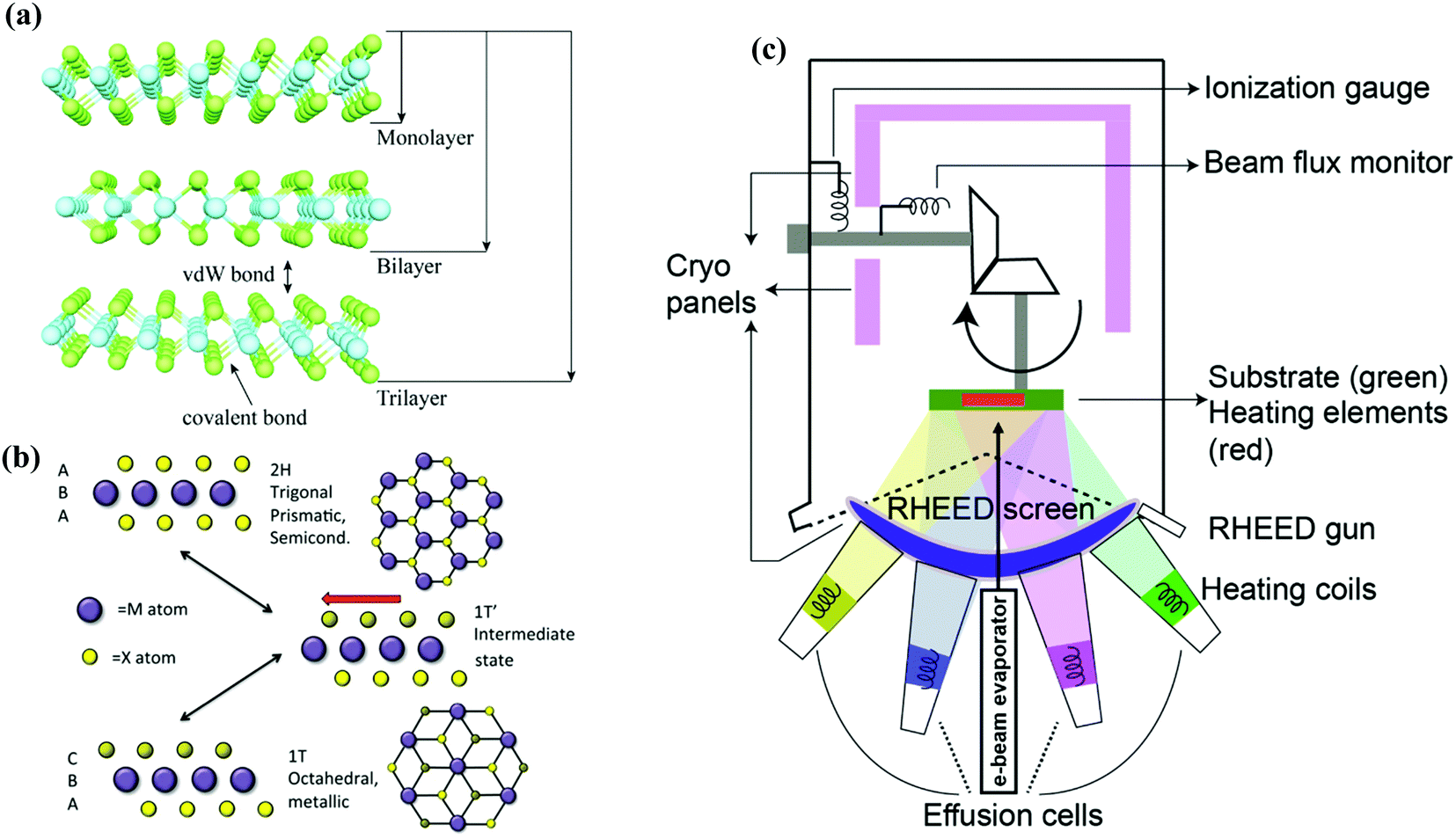 | ||
| Fig. 1 (a) Schematic depicting multiple layers of MoS2. Atoms of Mo are bonded via covalent bonds with S atoms. The individual layers are stacked together and held by weak vdW forces to form multi-layered or bulk structures. The figure has been reproduced from ref. 10. (b) Different crystal structures of MX2, showing different stacking sequences. The two most common phases 2H and 1T, as well as the intermediate 1T′ phase, are shown. The figure has been reproduced from ref. 75. (c) Schematic diagram showing the various components of an MBE system. The figure has been adapted and reproduced from ref. 62. | ||
Through the persevering efforts of researchers over the past few years, various techniques have been evolved to produce atomically ultrathin TMDCs.9,10 In general, these synthesis techniques can be classified into two groups: the first method, known as the top-down technique, produces TMDC flakes by thinning their bulk crystals. Different kinds of exfoliations fall in this group.9,54,68,69 Since different monolayers of 2D TMDCs are held together by weak inter-layer vdW forces, under external perturbation, bulk 2D TMDC crystals readily get reduced into their few-layered flakes. The second approach is to grow layered TMDCs via bottom-up techniques, wherein the constituent species assemble to form continuous thin films. The main techniques under this category are atomic layer deposition,70 magnetron sputtering,71 chemical vapor deposition (CVD),42,56 pulsed laser deposition (PLD),36 and MBE.72
Among these methods, MBE is a very promising synthesis technique used to grow epitaxial thin films and heterostructures, where fine control over the layer thickness and ultra-high purity of the material components are required.73,74 MBE involves the production of molecular/atomic beams of constituent source materials and/or doping species, which then react on the surface of a substrate to form an ordered thin film in an ultrahigh vacuum environment. The composition of this epitaxial thin film and its doping (if any) depends upon the arrival rate of the molecules/atoms and dopants, respectively. A typical MBE system consists of a stainless-steel ultrahigh vacuum chamber and various components such as vacuum pumps, substrate heater, effusion cells, etc. The source materials, usually of ultra-high purity (99.99%), are kept inside effusion cells (known as the Knudsen cells or K-cells). In the case of TMDCs, the transition metals are generally supplied from an e-beam evaporator, while the chalcogenides are placed inside these Knudsen cells.72 Appropriate substrates are heated to the desired growth temperature and usually rotated to improve the uniformity and homogeneity of the final product. These Knudsen cells are then heated to high temperatures, depending on the required growth rates, the composition of the product, and the doping concentrations. The schematic of a typical MBE system is shown in Fig. 1(c), depicting the different components and the three zones where various physical phenomena occur. The details of the various processes in these zones have been described elsewhere.62 The usual growth rates in an MBE process are a few hundred nm h−1 in contrast with other techniques where the growth rates are in the range of mm h−1, thereby allowing the grown interfaces to be precisely controlled in their compositions. In addition, due to lower arrival rates of the species on the substrates, the growth is highly controlled along with the negligible probability of back-sputtering of the deposited film, which results into very smooth films with high control over the surface damage.
3. Recent advances in MBE-grown transition metal dichalcogenides
In this section, an overview is presented describing the recent progress in the field of MBE-grown TMDCs. Thin-film growth by MBE possesses the potential to isolate monolayers of TMDCs and synthesize large-area ultrathin films, which otherwise cannot be easily produced by exfoliation or other growth techniques. The growth of epitaxial TMDC films by MBE dates back to the mid-1980s.76–78 These pioneering works have been done by Koma et al.77 where they have demonstrated the growth of epitaxial NbSe2 thin films, for the first time, on a cleaved 2H MoS2 surface, following which, Koma et al.78 successfully grew epitaxial MoSe2 thin films on a CaF2(111) substrate. In both reports, the in-plane crystallographic axes of the grown thin films showed a high alignment towards the axes of the substrates used for their growth, despite the large lattice mismatches (∼20%). Thus, the authors coined the term as “vdW epitaxy,” although extensive characterizations on the properties of these thin films were not carried out at that time. However, after almost three decades, recent research on different TMDCs has resurrected the concept of vdW epitaxy, and indeed there is an increasing number of research articles in this area being published in the last few years.63–65,79 For instance, similar to the works carried out by Koma et al.,77,78 Kreis et al.80 have applied scanning tunnelling microscopy (STM) and angle-resolved photoemission spectroscopy (ARPES) to evaluate the electronic valence band spectra of HfS2, during different stages of its epitaxial growth on WSe2. In another report, Kreis et al.81 have investigated the unoccupied and occupied electronic structures of HfS2 ultrathin films, by employing combined angle-resolved photoemission and inverse photoemission, along with the band structure calculations. They have studied the impact of the thickness of the film on the two- and three-dimensional conduction and valence band states. Thus, a lot of research is being done in the field of MBE-grown TMDCs and in the coming subsections, the recent progress has been discussed.3.1 Growth of selenides
In one of these early works, Barton et al.82 have reported the growth of monolayer HfSe2 on different substrates using MBE and have shown that this vdW epitaxy method allows the growth of high-quality heterostructures, without any strain or misfit dislocations in the thin films, in spite of the large lattice mismatch. Fig. 2(a) shows the high angle annular dark-field (HAADF) scanning transmission electron microscopy (STEM) image of HfSe2 on MoS2 grown by MBE. Peng et al.83 have shown a nearly layer-by-layer growth of TiSe2 ultrathin films on graphitized SiC(0001) substrate via MBE and have analyzed the defect structures of these films. The chemical inertness of graphene ensures a sharp interface between TiSe2 thin films and SiC. The STM measurements reveal the identification of two dominant types of Se vacancies and interstitial defects (Fig. 2(b–d)).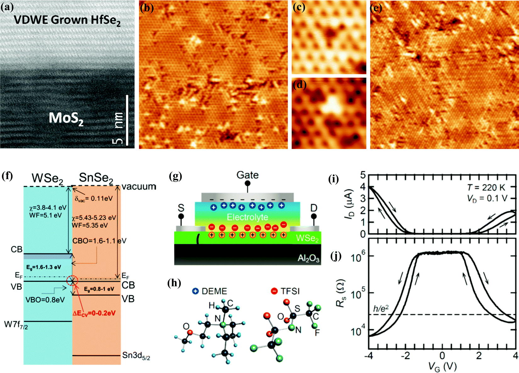 | ||
| Fig. 2 (a) HAADF-STEM image of HfSe2 grown on MoS2 by MBE. The figure has been reproduced from ref. 82. (b) STM micrograph of TiSe2 thin film (17 nm × 17 nm, I = 100 pA, and VS = 0.24 V), showing the two kinds of Se defects: bright Se interstitials and dark Se vacancies. Zoomed-in STM micrographs of a single (c) Se vacancy and (d) interstitial (2 nm × 2 nm, I = 100 pA, and Vs = 0.24V). (e) STM micrograph of a charge density waves (CDW)-related 2 × 2 superstructure in single-layer TiSe2 thin film (20 nm × 20 nm, I = 100 pA, and VS = 0.1 V). The figures have been reproduced from ref. 83. (f) Schematic of the band alignment at the WSe2/SnSe2 heterojunction as revealed by X-ray photoelectron spectroscopy (XPS) core level analysis. EF and χ denote the Fermi energy and electron affinity, respectively. Eg is the band gap, whereas VBO and CBO denote the valence and conduction band offsets, respectively. The figure has been reproduced from ref. 84. (g) Schematic of the top-gated electric-double-layer transistor (EDLT) based on the WSe2 epitaxial thin film grown on the sapphire substrate. (h) Chemical structure of the electrolyte used in the electrolyte-gated transistor. (i and j) show typical transfer characteristics of WSe2-EDLT carried out at T = 220 K, indicating clear ambipolar operation. The figures have been reproduced from ref. 79. | ||
Moreover, the observation of charge density waves (CDW) persisting down to monolayer TiSe2, as shown in Fig. 2(e), favors the mechanism of the excitonic insulator in TiSe2 thin films. These were a few early reports demonstrating the potential of the MBE as a growth technique for the production of TMDCs. In another report, Aretouli et al.84 have shown the growth of high-quality vdW heterostructures of SnSe2/WSe2 by MBE on AlN/Si(111) substrates using Bi2Se3 as a buffer layer. 1T polytype of SnSe2 is obtained having an indirect band gap of ∼0.8 eV with a strong and unintentionally doped n-type behavior. In contrast, the MBE-grown WSe2 stabilizes in the 2H phase, exhibiting a p-type behavior. Band offsets analysis of this heterojunction revealed a nearly broken gap heterostructure as depicted in Fig. 2(f), which can be suitable for designing tunneling field-effect electronic devices. It must be noted that other groups have reported mid-gap or even slightly above mid-gap Fermi levels for MBE-grown epitaxial WSe2 thin films, which correspond to an n-type behavior. For instance, Zhang et al.85 have shown the successful synthesis of WSe2 ultrathin films on an epitaxial bilayer graphene substrate with controlled film thickness at the atomic level. Employing in situ ARPES measurements, they have demonstrated the evolution of the electronic structure of the epitaxial WSe2 thin films, which confirms a direct band gap for the single layer and bilayer WSe2, and an indirect band gap for three or more layers of WSe2. From the scanning tunnelling spectroscopic (STS) measurements, it is observed that an asymmetry exists between the valence band maximum and conduction band maximum, with respect to the Fermi level, revealing slightly n-type doping of the grown WSe2 films. In another report, Blades et al.86 have comprehensively studied the electronic and geometric structure of defects in WSe2 thin films grown on highly oriented pyrolytic graphite (HOPG) with STS and STM, and the effect of temperature on the nature of these defects. In 2018, Wang et al.87 reported the transport properties of highly crystalline epitaxial TiSe2 thin films on a sapphire substrate grown by MBE. Robust CDW transitions have been demonstrated, down to 5 monolayers of TiSe2 thin films, highlighting an exciting phenomenon of in-plane self-rotational growth of the epitaxial thin film with respect to the substrate. Yan et al.88 have shown the successful growth of high-quality epitaxial PtSe2 thin films with controlled thickness by MBE for the first time. In another work, Nakano et al.79 have presented a study that demonstrates epitaxial and layer-by-layer growth of WSe2 thin films on sapphire by MBE, utilizing an optimized growth recipe. They have also shown the ambipolar transistor operation of these thin films by an electrolyte gating technique (Fig. 2(g–j)). The enhancement in the drain current (ID) is observed to be larger at the negative gate bias (VG), which corresponds to the hole-doped regime compared to the positive gate voltages, corresponding to the electron-doped regime. Consequently, the four-probe sheet resistance (RS) is found to be lower at the hole-doped side. The obtained results provide a benchmark towards the growth of epitaxial and large area TMDC thin films for scalable devices. In a recent report by Freedy et al.,89 the interfacial electrical resistance, interface chemistry, Seebeck coefficient, and thermal conductance of Ti, TiOx, and Ti/TiOx contacts to the MBE-grown WSe2 thin films have been carried out. Metallic Ti exhibits a strong chemical reactivity with WSe2 and results in W–Se bond scission, producing Ti–Se chemical states and metallic W. In addition, a high thermal boundary conductance along with low electrical resistance is also observed. On the other hand, TiOx exhibits low reactivity, lower thermal boundary conductance, and higher electrical resistance. Due to the extremely small thermal conductance obtained and the Ohmic nature of the metal contacts, this interface may be promising for thermionic and thermoelectric applications. So, these works on MBE-grown TMDCs have shown promise to fabricate a variety of wafer-scale TMDC thin films and heterostructures in a carefully controlled manner, thereby, opening a route towards intensive fundamental and applied science research on TMDC-based structures.
One of the TMDCs that has been readily explored by MBE is MoSe2.90,91 Roy et al.92 have reported the growth of MoTe2 and MoSe2 thin films on sapphire substrates and studied the temperature-dependent transport measurements of these thin films. The distinct layered structure of MoTe2 thin films is apparent from the high-resolution cross-sectional transmission electron microscopy (HR-XTEM), along with the abrupt interface formed with the substrate, as shown in Fig. 3(a). The hexagonal lattice arrangement of the atoms has been shown in the plan-view TEM image in Fig. 3(b), and a lattice constant of 3.5 Å is extracted, which matches with that of bulk 2H MoTe2. Fig. 3(c) shows the plan-view TEM micrograph of the MoSe2 thin film, depicting a hexagonal lattice arrangement of atoms. The derived lattice constant of 3.3 Å is in good agreement with that of the bulk 2H MoSe2. Moreover, an insulating behavior is observed for the grown thin films, which is in good agreement with 2D-variable range hopping (VRH), suggesting that the charge transport in these thin films is governed by the localized charge-carrier states (Fig. 3(d and e)). In another report, Chen et al.72 have grown atomically thin, highly oriented, and ambipolar monolayer MoSe2 on GaAs(111)B substrates. They have realized an electrolytically-gated transistor based upon the transferred MoSe2 thin film (Fig. 3(f and g)), and it is perceived that the electrical transport characteristics of the device also follow the 2D-VRH (Fig. 3(h and i)) because of the disorders in the thin film. Ma et al.93 have shown that twin grain boundaries in MBE-grown MoSe2 thin films on different substrates are metallic in nature, substrate-independent, and undergo a Peierls metal to insulator transition at low temperatures. By utilizing STS measurements, substantial band gap narrowing of the MoSe2 thin film is observed in the vicinity of these grain boundaries, which might be due to the stress induced within the film. It has been demonstrated in other reports that these twin boundaries in MoSe2 have excess incorporation of Mo-atoms, which is a possible method for modifying MoSe2 basal planes and consequently, altering their properties to potentially enhance their application in selective water adsorption.94 Various other groups have also demonstrated the growth of MoSe2 thin films on different 2D substrates, such as hexagonal boron nitride.95 In a recent report, He et al.96 have shown the gate-tuneable phonon properties of 2H MoSe2 grown via MBE. The study demonstrates the electrostatically enhanced electron–phonon interactions in monolayer MoSe2 thin films. It focuses on the correlation between the phonon properties and multiple valleys of monolayer and bilayer MoSe2 thin films at different doping levels. The monolayer MoSe2-based ion-gated devices also exhibit typical n-type transport characteristics with a high on/off ratio of ∼105, along with a mobility of ∼31 cm2 V−1 s−1.
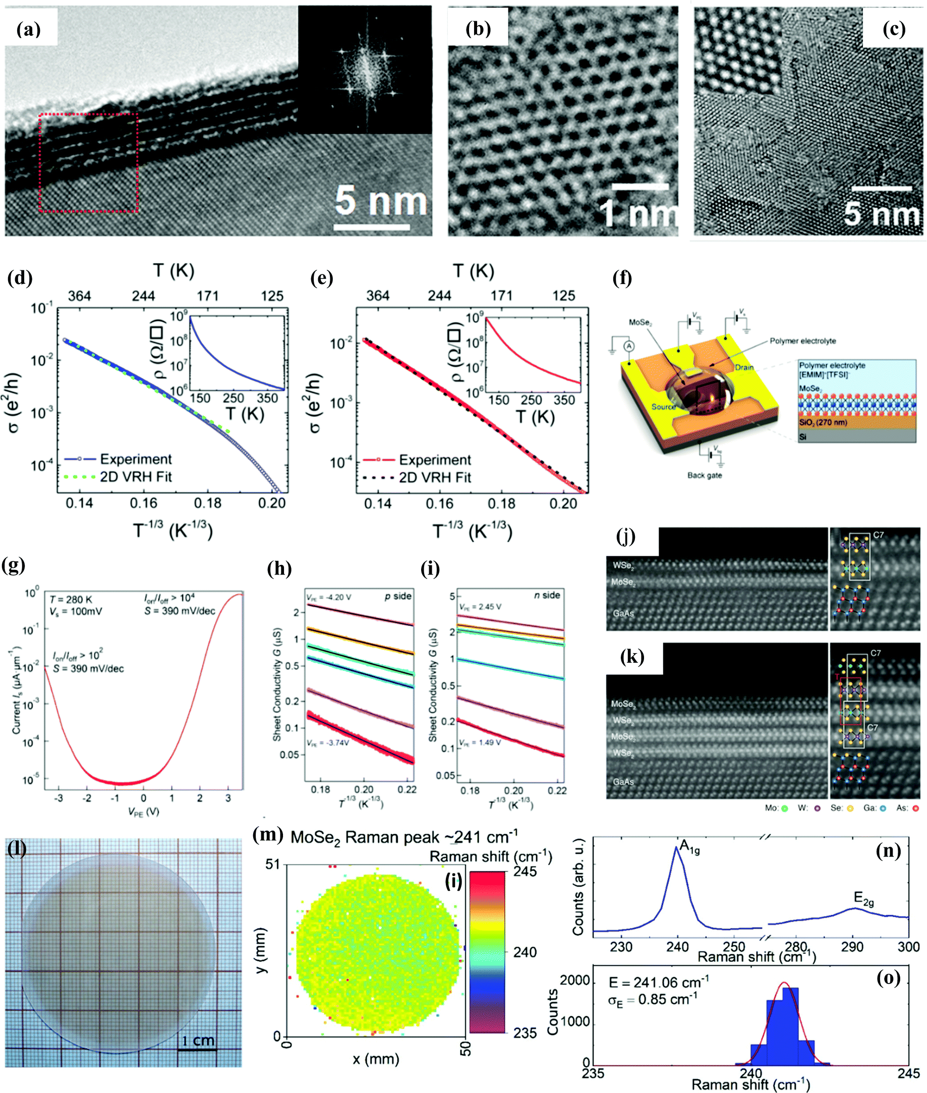 | ||
| Fig. 3 (a) HR-XTEM image of a layered structure of MoTe2. Inset shows the fast Fourier transform (FFT) of the area marked by the red square. The plan-view TEM image depicts the hexagonal arrangement of atoms in the (b) MoTe2 thin film and (c) MoSe2 lattice. Inset shows the zoomed-in view for 2 × 2 nm2. Electrical transport measurements show the conductivity variation with T−1/3 for (d) MoTe2 and (e) MoSe2. Insets of (d, e) show the variations of the measured resistivities with temperature. The figures have been reproduced from ref. 67. (f) The schematic device structure of the MoSe2 thin film-based EDLT. (g) Variation of the channel current with polymer electrolyte voltage (VPE) depicting ambipolar behavior. (h and i) Sheet conductivity (GSH) as a function of T−1/3 on the p and n sides for different values of VPE. The figure has been reproduced from ref. 45. The HAADF-STEM images for the (j) bilayered WSe2/MoSe2 and (k) four-layered MoSe2/WSe2 heterostructures grown on GaAs(111)B. The figure has been reproduced from ref. 71. (l) Optical image of epitaxially grown MoSe2. (m) Peak energy of the A1g mode obtained through Raman mapping. (n) Typical Raman spectrum of MoSe2. (o) Distribution of the peak energy of the A1g mode indicating the mean value and standard deviation. The figure has been reproduced from ref. 73. | ||
Recently, Ohtake et al.97 have successfully fabricated large-area 2D highly oriented WSe2/MoSe2 and MoSe2/WSe2 heterostructures using MBE, comprising consecutively stacked epitaxial WSe2 and MoSe2 monolayers on GaAs(111)B substrates, which have been pre-treated with Se. Fig. 3(j) displays the HAADF-STEM image of the MBE-grown bilayered WSe2/MoSe2 heterostructure, depicting the distinct layered structure. TMDC bilayered heterostructures can have several basic stacking geometries. In the most fundamental stacking geometry, the metal/chalcogen atoms of the first TMDC layer are on top of metal/chalcogen atoms of the second TMDC layer, where the T stacking geometry is obtained by the translation of the fundamental stacking sequence in such a way that the metal atoms of one of the TMDC layers are on top of the hexagonal centers of the other TMDC layer. In contrast, the C7 stacking geometry can be obtained from the T stacking via rotation of one TMDC layer concerning the other layer by an angle of 180° about the axis, which crosses a pair of overlapped chalcogen and metal atoms of the two TMDC layers (the metal atoms go on top of the chalcogen atoms and the chalcogen atoms go on top of the metal atoms).98 The magnified image (shown on the right in Fig. 3(j)) confirms the formation of a C7-stacking configuration. In contrast, in the four-layered MoSe2/WSe2 heterostructure, as shown in Fig. 3(k), two kinds of stacking sequences, i.e., C7 and T, are observed. The simultaneous formation of the T stacking configuration could be attributed to the small difference in the energies between the T and C7 stacking sequences for the MoSe2/WSe2 heterostructure. In other reports, wafer-scale growth of MoSe2 has been achieved on a h-BN/sapphire substrate at a low growth temperature by combining the techniques of metal-organic vapor phase epitaxy (MOVPE) and MBE, revealing a large uniformity and homogeneity of the grown heterostructure on the whole wafer through an in-depth examination of the optical studies (Fig. 3(l–o)).99 Recently, Wei et al.100 have shown the complex nature of the nucleation and growth processes of MoSe2 monolayers grown via MBE on mica. It has been observed that the 1T phase of MoSe2 forms along with a comparable quantity of the 2H phase of MoSe2, where the 1T phase converts gradually into the stable 2H phase before the complete growth of the first monolayer. These results demonstrate the possibility of stabilizing the metastable phases of atomically thin TMDCs by MBE.
3.2 Growth of sulfides
Recently, extensive research has also been focused on the growth of sulfides, such as MoS2 thin films, utilizing MBE. Fu et al.101 have performed the growth of MoS2 on h-BN under thermodynamically controlled conditions, which allow MoS2 grains to align epitaxially on an h-BN substrate having the same orientation, thus, merging perfectly without the formation of grain boundaries. In another report, El Kazzi et al.102 have presented large-area growth of MoS2 on 200 mm SiO2/Si and Al2O3/Si templates using gas source MBE and have analysed the effect of the underneath surface template on the crystallinity of the MoS2 layers. The HRTEM and HAADF-STEM images of MoS2 on Al2O3/Si and MoS2 on SiO2/Si are shown in Fig. 4(a and b). The HRTEM images show the presence of a strong disorder in the MoS2 thin film with clear crossing and overlapping of the atomic planes, which is because of the formation of small grains (∼10 nm diameter). The energy dispersive spectroscopy (EDS) line profile shown in Fig. 4(b) reveals a small concentration of atomic Mo beneath the native oxide layer, indicating that Mo diffusion takes place through the thin native SiO2 layer during the MoS2 film deposition. On the other hand, this diffusion does not occur when an Al2O3 template is used (Fig. 4(a)), thereby efficiently blocking the diffusion of both Mo and S through the oxide layer. Xu et al.103 have performed growth of 1H and 1T′ phases of nanosized MoS2 islands on an Au(111) substrate by MBE and have analyzed the polymorph evolution by modulating the growth fluxes of Mo and S. A band gap opening of 80 meV at cryogenic temperatures (∼4.5 K) for the 1T′ phase is noticed, which is in agreement with the predicted quantum spin Hall characteristics for the 1T′ phase of MoS2. Fig. 4(c) shows the STS measurements of the 1T′ MoS2 islands taken at the center, depicting a small band gap instead of the sharp V shape. The zoomed-in dI/dV curves taken at the edge and center of 1T′ islands are shown in Fig. 4(d), clearly indicating an energy gap opening of 75 ± 5 meV at the center. In another report, Ehlen et al.104 have demonstrated the growth of epitaxial MoS2 on a graphene/Ir(111) substrate and have reported a detailed spectroscopical analysis of this epitaxial system. A photoluminescence spectrum with a narrow peak width (∼18 meV) has been observed. It was explained based on weak MoS2–graphene interaction, preventing PL quenching, usually expected for metallic substrates. Mortelmans et al.105 have studied the epitaxial growth of MoS2 on sapphire and exfoliated MoS2 flakes via MBE and MOVPE, and the analysis reveals that the technique of MBE yields superior epitaxial MoS2 quality as compared with MOVPE. However, it was noticed that MBE provides greater control on the epitaxial registry in both cases. Recently, Ermolaev et al.106 have presented a detailed study on the structural and optical properties of a monolayer of MoS2 thin films grown by MBE on sapphire. The analysis has shown that the MBE-grown MoS2 film exhibits a two-fold greater quantum yield of PL and lower photobleaching when compared with the CVD-synthesized MoS2 films (Fig. 4(e)), thereby, making it a promising candidate for photonic applications.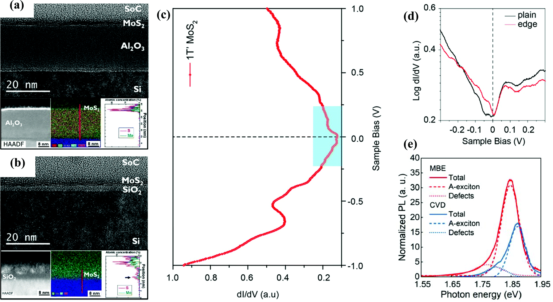 | ||
| Fig. 4 The HR-TEM and HAADF-STEM images and the corresponding EDS mappings of (a) MoS2 on Al2O3/Si and (b) MoS2 on SiO2/Si. The line profiles (red in color) in the EDS maps probe the concentrations of Mo and S atoms along the film/substrate interface. The figures have been reproduced from ref. 102. The electronic structure of the MBE-grown 1T′-MoS2 nanocrystals at 4.5 K. (c) STS measurements taken at the bulk (center) of the 1T′-MoS2 nanocrystals. (d) Zoomed-in views of the STS measurements of the 1T′-MoS2 nanocrystals taken at the bulk and edge. The figure has been reproduced from ref. 103. (e) The PL spectra of the CVD and MBE-grown single-layer MoS2 on Al2O3 substrates. Dotted and dashed lines indicate the deconvolution of the PL spectra into Gaussian peaks corresponding to defects and A-excitons, respectively. The figure has been reproduced from ref. 106. | ||
3.3 Growth of tellurides
In addition, apart from the transition metal sulfides and selenides, researchers have also started exploring transition metal tellurides grown by MBE. Yu et al.107 have reported the growth of continuous MoTe2 thin films (atomically thin heterophase, homojunctions) across graphene substrates through MBE and have obtained the stoichiometric 2H and 1T′ phases of MoTe2 simultaneously, showing potential for novel phase-patterning applications. The STS measurements performed on the thin films (from points A to G as shown in Fig. 5(a)) reveal “V”-type curves that gradually transform into “U”-type curves from point A to point G (differential conductance spectra shown in Fig. 5(b)). These results suggest the coherent phase transformation taking place from the semimetallic 1T′-MoTe2 into the semiconducting 2H-MoTe2. Walsh et al.108 have reported the first-ever growth and characterization of WTe2 thin films by MBE on several 2D substrates, including Bi2Te3, MoS2, and graphite, and have enabled the growth of WTe2 thin films in the distorted octahedral phase via interrupting the beam of the metal source. In another report, Li et al.109 have discussed the growth of high-quality and epitaxial PdTe2 thin film on a bilayer graphene/SiC(0001) substrate by MBE and have characterized this atomically thin film using STM. PdTe2 has recently stimulated considerable research interest because of the underlying physics associated with this material system, as it exhibits the coexistence of both type-II Dirac fermions and superconductivity. ARPES measurements of a six-layered PdTe2 thin film reveal a type-I Dirac cone contributing from Z2 topological surface states and their metallicity. Similarly, PtTe2 is a type-II Dirac semimetal and exhibits unique photodetection capability in the mid infrared (MIR) region and robust ambient stability. Wei et al.110 have recently shown large area and high-quality 1T-PtTe2 monolayer thin films grown by MBE with excellent air stability. It is observed that a PtTe2-based photodetector displays a photoresponse in a broad spectral range with high photoresponsivity and specific detectivity. The transmission electron microscopy (TEM) images of the grown PtTe2 depict the hexagonal arrangement of the Pt and Te atoms with lattice spacings of 0.20 and 0.35 nm, corresponding to the (110) and (100) planes of the hexagonal phase of PtTe2, respectively, as shown in Fig. 5(c–e). The PtTe2-based photodetector shows a broadband photoresponse (bias voltage of 0.1 V) in the wavelength range of 420 nm–10.7 μm, exhibiting responsivities of 1.6 and 0.2 mA W−1 at 4.7 and 10.7 μm, respectively, as shown in Fig. 5(f and g). The three photoresponse cycles (Fig. 5(f)) maintain similar responsivities and noise levels, indicating stable and repeatable photodetection. In addition, these photodetectors also exhibit high sensitivity in the near infrared and visible regions.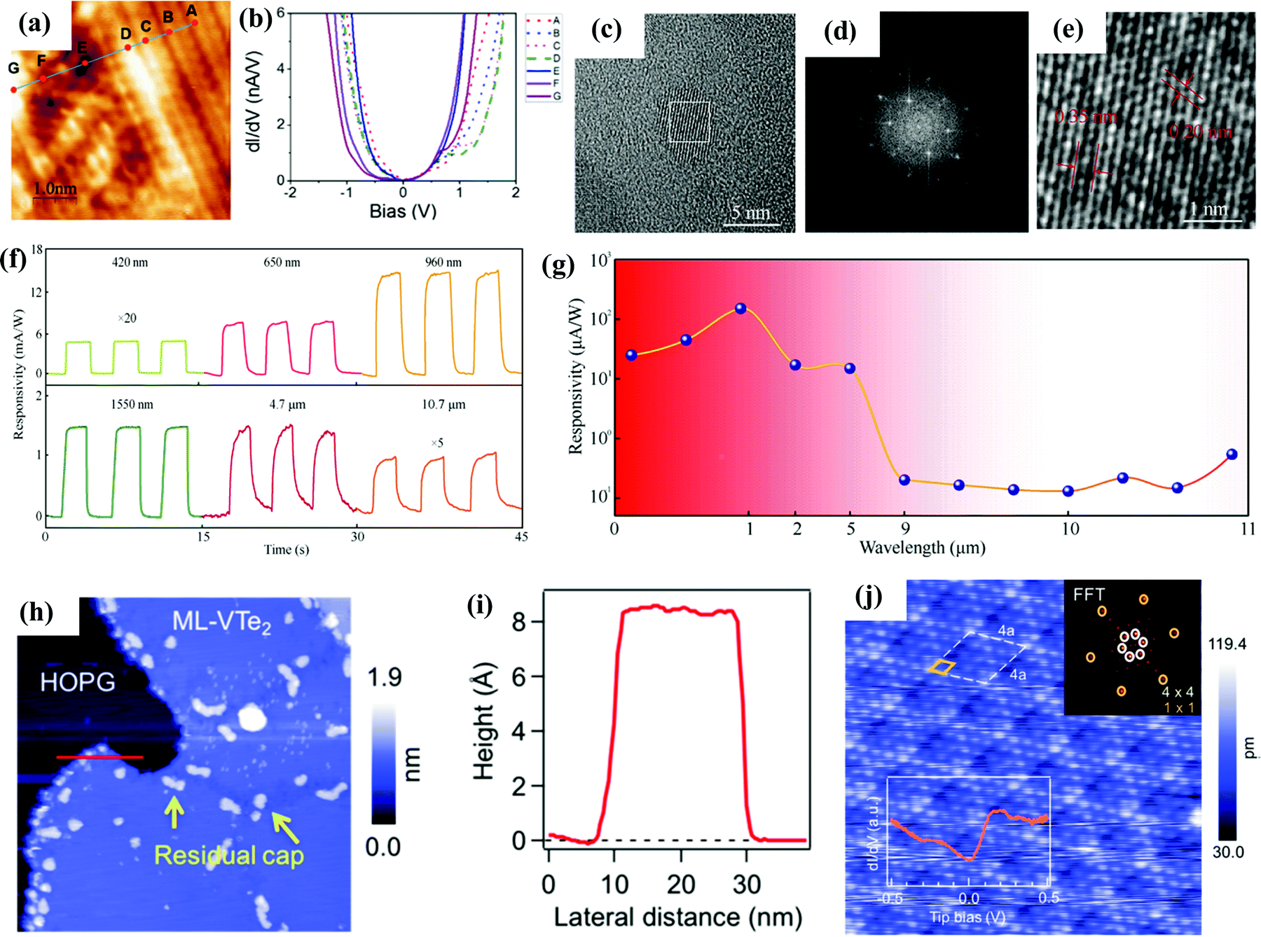 | ||
| Fig. 5 (a) Atomic-resolution STM image (It = 300 pA, Vb = 500 mV) and the corresponding (b) STS curves of the 2H-1T′ MoTe2/graphene ultrathin films. The figures have been reproduced from ref. 107. (c) The HRTEM image of the 1T-PtTe2 thin film. (d) The zoomed-in image of the marked area in (c). (e) FFT of the layered 1T-PtTe2 structure is shown in (d). (f) Spectral photoresponse of the PtTe2. (g) Broadband photoresponse at different wavelengths (as indicated in the figure). The magnitudes of low responsivities (420 nm and 10.7 μm) have been multiplied for better visualization. The figure has been reproduced from ref. 110. (h) The STM image of monolayer VTe2 measured at 77 K (150 × 150 nm2; tunnelling current = 68 pA, tip bias = −0.89 V). Residual caps have been marked by yellow arrows. (i) A step height of ∼8.5 Å indicates monolayer VTe2 as shown in the line profile in (h). (j) The STM image showing atomic-resolution (10 × 10 nm2; tunnelling current = 150 pA, tip bias = +0.1 V). The figure has been reproduced from ref. 112. | ||
Other transition metal di-tellurides to be successfully grown by MBE include monolayers of VTe2, TiTe2, and CrTe2. In one such report, Lasek et al.111 have shown that monolayer synthesis of 1T-TMDCs could be realized for all three early transition metal (Ti, V, and Cr) ditellurides via MBE, including the growth of CrTe2, which is metastable only in its bulk form. In another report, Wong et al.112 have presented direct spectroscopic and microscopic evidence of d1 electronic configuration and metallic phase (1T) in monolayer VTe2 grown by MBE on HOPG and a (4 × 4) CDW reconstruction pattern is obtained (Fig. 5(h–j)), different from the double zigzag chains observed in the bulk structure. Regarding the magnetic properties of the monolayer VTe2, the X-ray magnetic circular dichroism (XMCD) measurements exclude the presence of an inherent ferromagnetic ordering, which contradicts the previous theoretical predictions.
3.4 Growth of chalcogenide-based alloys
Recently, 2D material-based alloys have also been investigated as they can represent a versatile platform that can extend the properties of the existing atomically thin TMDCs to the next level. Xie et al.113 have realized the MBE growth of monolayer MoxW1−xSe2 alloys with controllable values of stoichiometric ratio. Utilizing in situ ARPES and XPS, the modifications in the valence band dispersion and the size of the spin-splitting have been determined by modulating the Mo/W ratios, as illustrated in Fig. 6(a–h). The growth of monolayers of these MoxW1−xSe2 alloys by MBE and the growth recipe for controlling the stoichiometric ratio paves an effective method for band structure engineering and spin-splitting in the 2D AB2 family. Similarly, Zhang et al.114 have investigated the synthesis of VxMo1−xSe2 alloys by MBE on HOPG. A systematic study on the evolution of magnetism, electronic structure, and the thermal stability of VxMo1−xSe2 alloys has been presented. Essentially, a critical value of x (∼0.44) has been observed, above which the system remains as a homogeneous metallic phase and below which, separation of phases is favoured. Low vanadium concentrations (x ≤ ∼0.05) effectually increase the density of mirror twin boundaries in MoSe2. Fig. 6(i–m) depict the evolution of the morphology of the 2D VxMo1−xSe2 alloys and as the value of x increases, the crystalline domains gradually evolve from leaf-like (MoSe2) into the triangular (VSe2) form. The XMCD measurements show the absence of ferromagnetism down to 65 K, both in VxMo1−xSe2 alloys and monolayer VSe2. Thus, these works provide a comprehensive understanding of the electronic structures and properties of 2D TMDC alloys, which can be useful for designing futuristic 2D electronic devices.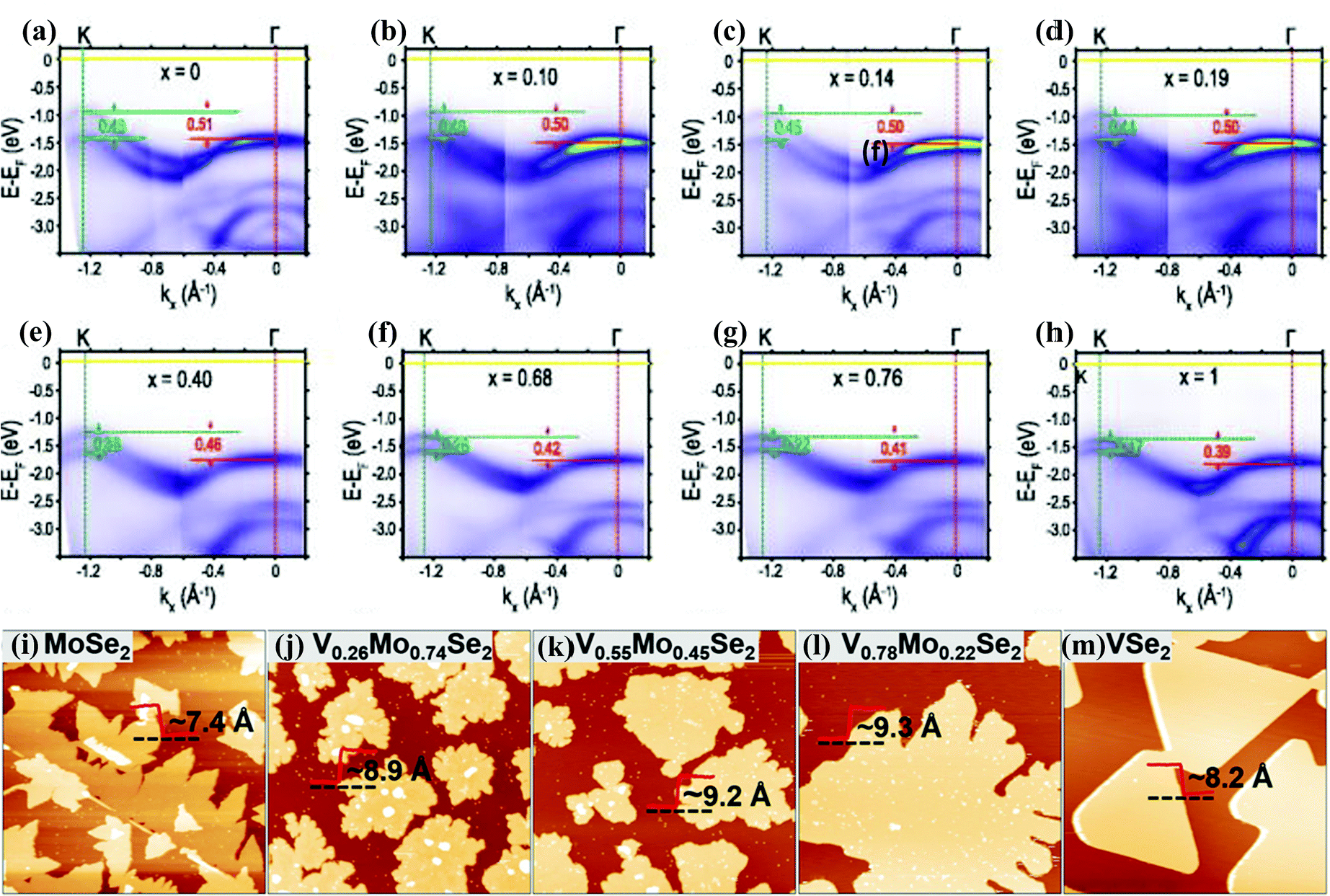 | ||
| Fig. 6 The ARPES spectra of monolayer MoxW1−xSe2 thin films measured along the Γ–K direction with different Mo ratios (as indicated). The Mo ratios (x) in MoxW1−xSe2 from (a–h) can be stoichiometrically displayed as: (a) WSe2, (b) Mo0.10W0.90Se2, (c) Mo0.14W0.86Se2, (d) Mo0.19W0.81Se2, (e) Mo0.40W0.60Se2, (f) Mo0.68W0.32Se2, (g) Mo0.76W0.24Se2, and (h) MoSe2. The, green, yellow, and red lines indicate the energy levels at the K point, Fermi level, and C point, respectively. The energy difference between the K and Γ points, and the spin-splitting at the K point are also shown in (a–h). The figures have been reproduced from ref. 113. The STM and STS images of VxMo1−xSe2 alloys (250 × 250 nm2): (i) MoSe2, (j) V0.26Mo0.74Se2, (k) V0.55Mo0.45Se2, (l) V0.78Mo0.22Se2, and (m) VSe2 (set points: (i) −3.8 V, 10 pA; (j) 1.6 V, 17 pA; (k) 1.6 V, 23 pA; (l) −1.6 V, 5 pA; (m) −0.5 V, 44 pA). The figure has been reproduced from ref. 114. | ||
4. Summary and outlook
Recent years have witnessed remarkable progress in the MBE growth of a variety of TMDC thin films. In this article, we have discussed the fundamental properties of TMDCs, along with a brief review of the standard synthesis methods used for their fabrication. A short discussion on MBE has followed this, and finally, a progressive conversation regarding the MBE-growth of various TMDCs has been presented. These results unquestionably show the potential of MBE as one of the most promising and reliable techniques for the growth of high-quality TMDCs and contribute towards the advancement in the applications based on TMDCs in the future.The published literature in this field indubitably indicates the substantial progress of TMDCs grown by MBE; however, the potential of this special class of materials still needs to be fully unearthed. Hence, a perspective and the associated follow-up research have been given below and illustrated in Fig. 7.
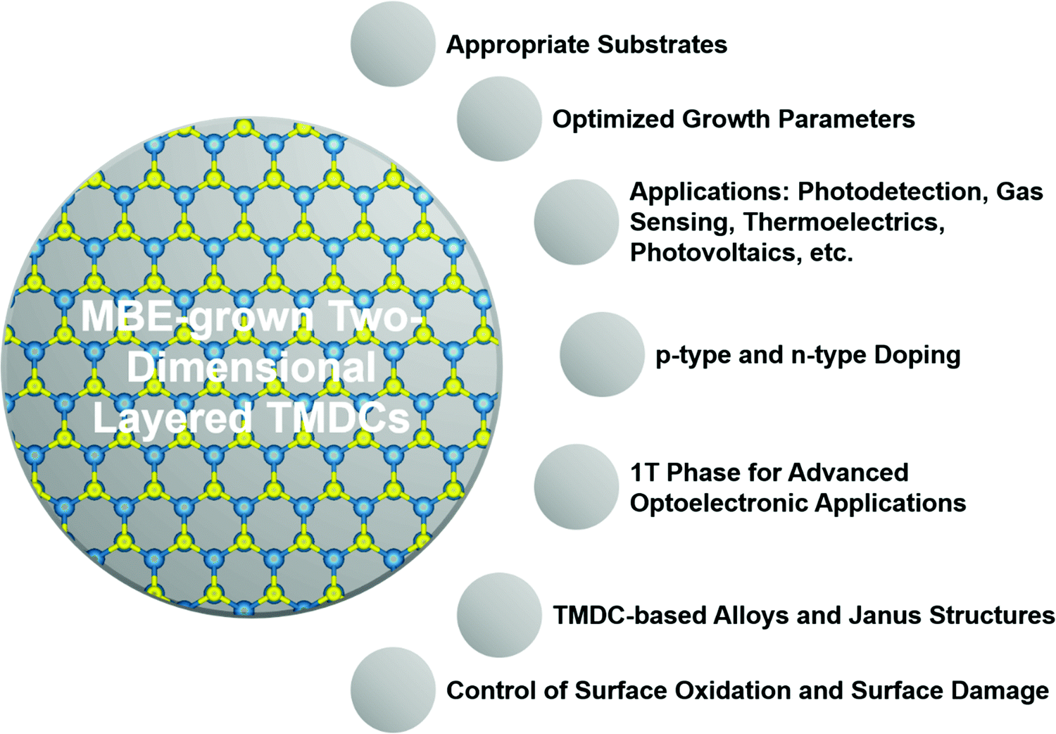 | ||
| Fig. 7 Schematic illustrating the current prospects and opportunities to be explored in the field of MBE-grown TMDCs. | ||
• The investigations on the MBE-fabricated TMDCs are still in the nascent phase, because of the recent popularity of MBE for the synthesis of TMDCs, in comparison to the other conventional synthesis techniques such as exfoliation and CVD. Thus, there still exists plenty of room for the enhancement of the crystal quality of these thin films by utilizing appropriate substrates for their growth and by further correlating the unexplored or much less explored growth parameters, for instance, the beam flux of the sources, annealing time, growth temperature, etc.86,111,115–117
• To date, most of the research in this field is limited to the growth of TMDC thin films and heterostructures. It is high time that focus needs to be given to fabricating MBE-grown TMDC-based devices, which can be promising in various applications such as photodetection, gas sensing, thermoelectrics, photocatalysis, energy generation, photovoltaics, etc.89,118–121
• Doping of MBE-grown TMDC thin films is another crucial area that needs to be explored in the future, which will help in enhancing the performance of TMDC-based devices. In addition, there is a great necessity to optimize p-type doping of TMDCs, which will be beneficial for the further growth of wide band gap n-type III-nitride semiconductors such as GaN or AlGaN to be utilized in p–n diodes, Esaki diodes, etc.122–124
• So far, promising results have been obtained in synthesizing semi-metallic phases of TMDCs (1T), which can be used in advanced optoelectronic applications, as they possess outstanding light absorption and electronic properties.75,103,110,112,125–127
• More research should be devoted to the study of TMDC-based alloys. Moreover, Janus TMDCs, which refer to transition metal layers with dissimilar surfaces, have engrossed intensive interest these days owing to their unique characteristics induced due to symmetry breaking and must be explored by MBE.113,114,128
• Even though the surfaces of TMDCs are more inert than those of non-layered materials, surface oxidation is still thermodynamically favored for TMDCs. Thus, the issue of surface oxidation needs to be solved and therefore, the study of the oxidation kinetics of the MBE-grown TMDCs can be an exciting area of investigation.129,130
As a concluding remark, MBE has emerged as a promising growth technique for large-scale TMDC thin films, and hence, holds the potential for use in next-generation device applications.
Conflicts of interest
The authors declare no conflicts of interest.Acknowledgements
The authors would like to convey sincere gratitude to the Director, CSIR-NPL, New Delhi, India for his constant support. D. K. S. is thankful to the SERB National Postdoctoral Fellowship (PDF/2021/002469) for providing financial support.References
- W. Li, X. Zhang, R. Meng, J. Yan, J. Wang, J. Li and T. Wei, Epitaxy of III-nitrides on β-Ga2O3 and its vertical structure LEDs, Micromachines, 2019, 10(5), 322 CrossRef PubMed.
- N. Senthilkumar, E. Vivek, M. Shankar, M. Meena, M. Vimalan and I. V. Potheher, Synthesis of ZnO nanorods by one step microwave-assisted hydrothermal route for electronic device applications, J. Mater. Sci.: Mater. Electron., 2018, 29(4), 2927–2938 CrossRef CAS.
- M. Mukherjee and A. K. Singh, Strong chemical bond hierarchy leading to exceptionally high thermoelectric figure of merit in oxychalcogenide AgBiTeO, ACS Appl. Mater. Interfaces, 2020, 12(7), 8280–8287 CrossRef CAS PubMed.
- A. Bapat, C. Anderson, C. R. Perrey, C. B. Carter, S. A. Campbell and U. Kortshagen, Plasma synthesis of single-crystal silicon nanoparticles for novel electronic device applications, Plasma Phys. Control. Fusion, 2004, 46(12B), B97–B109 CrossRef CAS.
- H. S. Bae, M. H. Yoon, J. H. Kim and S. Im, Photodetecting properties of ZnO-based thin-film transistors, Appl. Phys. Lett., 2003, 83(25), 5313–5315 CrossRef CAS.
- J. Saroha, S. Mehra, M. Kumar and S. N. Sharma, Thermo-physical properties of paraffin/TiO2 and sorbitol/TiO2 nanocomposites for enhanced phase change materials: a study on the stability issue, Appl. Phys. A: Mater. Sci. Process., 2021, 127(12), 916 CrossRef CAS.
- C. Pacholski, Photonic crystal sensors based on porous silicon, Sensors, 2013, 13(4), 4694–4713 CrossRef CAS PubMed.
- A. M. Chowdhury, G. Chandan, R. Pant, B. Roul, D. K. Singh, K. K. Nanda and S. B. Krupanidhi, Self-powered, broad band, and ultrafast InGaN-based photodetector, ACS Appl. Mater. Interfaces, 2019, 11(10), 10418–10425 CrossRef CAS PubMed.
- J. D. Yao, Z. Q. Zheng and G. W. Yang, Production of large-area 2D materials for high-performance photodetectors by pulsed-laser deposition, Prog. Mater. Sci., 2019, 106, 100573 CrossRef CAS.
- D. K. Singh, K. K. Nanda and S. B. Krupanidhi, Pulsed laser deposition of transition metal dichalcogenides-based heterostructures for efficient photodetection, in Practical Applications of Laser Ablation, ed. D. Yang, IntechOpen, London, 2021 Search PubMed.
- S. Das, A. Sebastian, E. Pop, C. J. McClellan, A. D. Franklin, T. Grasser, T. Knobloch, Y. Illarionov, A. V. Penumatcha, J. Appenzeller, Z. Chen, W. Zhu, I. Asselberghs, L.-J. Li, U. E. Avci, N. Bhat, T. D. Anthopoulos and R. Singh, Transistors based on two-dimensional materials for future integrated circuits, Nat. Electron, 2021, 4(11), 786–799 CrossRef CAS.
- A. Sebastian, R. Pendurthi, T. H. Choudhury, J. M. Redwing and S. Das, Benchmarking monolayer MoS2 and WS2 field-effect transistors, Nat. Commun., 2021, 12(1), 693 CrossRef CAS PubMed.
- M. Mishra, A. Dash, A. Sharma, M. Khanuja and G. Gupta, CO sensing properties of nanostructured WSe2/GaN and MoSe2/GaN based gas sensors, Phys. E, 2022, 115147 CrossRef CAS.
- T. F. Schranghamer, M. Sharma, R. Singh and S. Das, Review and comparison of layer transfer methods for two-dimensional materials for emerging applications, Chem. Soc. Rev., 2021, 50(19), 11032–11054 RSC.
- W. Zhu, T. Low, H. Wang, P. Ye and X. Duan, Nanoscale electronic devices based on transition metal dichalcogenides, 2D Mater., 2019, 6(3), 032004 CrossRef CAS.
- K. S. Novoselov, A. K. Geim, S. V. Morozov, D. Jiang, Y. Zhang, S. V. Dubonos, I. V. Grigorieva and A. A. Firsov, Electric field effect in atomically thin carbon films, Science, 2004, 306(5696), 666–669 CrossRef CAS PubMed.
- D. K. Singh, R. Pant, A. M. Chowdhury, B. Roul, K. K. Nanda and S. B. Krupanidhi, Defect-mediated transport in self-powered, broadband, and ultrafast photoresponse of a MoS2/AlN/Si-based photodetector, ACS Appl. Electron. Mater., 2020, 2(4), 944–953 CrossRef CAS.
- A. Kumar, M. A. Khan and M. Kumar, Recent advances in UV photodetectors based on 2D materials: A review, J. Phys. D: Appl. Phys., 2022, 55(13), 133002 CrossRef CAS.
- M. A. Ribas, A. K. Singh, P. B. Sorokin and B. I. Yakobson, Patterning nanoroads and quantum dots on fluorinated graphene, Nano Res., 2011, 4(1), 143–152 CrossRef CAS.
- P. Li, C. Wang, J. Zhang, S. Chen, D. Guo, W. Ji and D. Zhong, Single-layer CrI3 grown by molecular beam epitaxy, Sci. Bull., 2020, 65(13), 1064–1071 CrossRef CAS.
- A. Rambabu, D. K. Singh, R. Pant, K. K. Nanda and S. B. Krupanidhi, Self-powered, ultrasensitive, room temperature humidity sensors using SnS2 nanofilms, Sci. Rep., 2020, 10(1), 14611 CrossRef CAS PubMed.
- N. Goel and M. Kumar, 2D materials for terahertz application, Nano Ex, 2021, 2(3), 031001 CrossRef.
- P. Kumbhakar, C. Chowde Gowda, P. L. Mahapatra, M. Mukherjee, K. D. Malviya, M. Chaker, A. Chandra, B. Lahiri, P. M. Ajayan, D. Jariwala, A. Singh and C. S. Tiwary, Emerging 2D metal oxides and their applications, Mater. Today, 2021, 45, 142–168 CrossRef CAS.
- P. Kumbhakar, M. Mukherjee, A. Pramanik, S. Karmakar, A. K. Singh, C. S. Tiwary and P. Kumbhakar, Confinement aided simultanous water cleaning and energy harvesting using atomically thin Wurtzite (Wurtzene), Adv. Sustain. Syst, 2021, 5(2), 2000189 CrossRef CAS.
- D. K. Singh, R. Pant, B. Roul, A. M. Chowdhury, K. K. Nanda and S. B. Krupanidhi, Temperature-dependent electrical transport and optoelectronic properties of SnS2/p-Si heterojunction, ACS Appl. Electron. Mater, 2020, 2(7), 2155–2163 CrossRef CAS.
- T. Niu, New properties with old materials: Layered black phosphorous, Nano Today, 2017, 12, 7–9 CrossRef CAS.
- Y. Li, H. Wang, L. Xie, Y. Liang, G. Hong and H. Dai, MoS2 nanoparticles grown on graphene: An advanced catalyst for the hydrogen evolution reaction, J. Am. Chem. Soc., 2011, 133(19), 7296–7299 CrossRef CAS PubMed.
- R. Mas-Ballesté, C. Gómez-Navarro, J. Gómez-Herrero and F. Zamora, 2D materials: To graphene and beyond, Nanoscale, 2011, 3(1), 20–30 RSC.
- X. Zong, H. Yan, G. Wu, G. Ma, F. Wen, L. Wang and C. Li, Enhancement of photocatalytic H2 evolution on CdS by loading MoS2 as cocatalyst under visible light irradiation, J. Am. Chem. Soc., 2008, 130(23), 7176–7177 CrossRef CAS PubMed.
- K. Ellmer, Preparation routes based on magnetron sputtering for tungsten disulfide (WS2) films for thin-film solar cells, Phys. Status Solidi B, 2008, 245(9), 1745–1760 CrossRef CAS.
- D. Lembke, S. Bertolazzi and A. Kis, Single-layer MoS2 electronics, Acc. Chem. Res., 2015, 48(1), 100–110 CrossRef CAS PubMed.
- A. P. Nayak, S. Bhattacharyya, J. Zhu, J. Liu, X. Wu, T. Pandey, C. Jin, A. K. Singh, D. Akinwande and J.-F. Lin, Pressure-induced semiconducting to metallic transition in multilayered molybdenum disulphide, Nat. Commun., 2014, 5(1), 3731 CrossRef CAS PubMed.
- N. Perea-López, A. L. Elías, A. Berkdemir, A. Castro-Beltran, H. R. Gutiérrez, S. Feng, R. Lv, T. Hayashi, F. López-Urías, S. Ghosh, B. Muchharla, S. Talapatra, H. Terrones and M. Terrones, Photosensor device based on few-layered WS2 films, Adv. Funct. Mater., 2013, 23(44), 5511–5517 CrossRef.
- X. Zong, J. Han, G. Ma, H. Yan, G. Wu and C. Li, Photocatalytic H2 evolution on CdS loaded with WS2 as cocatalyst under visible light irradiation, J. Phys. Chem. C, 2011, 115(24), 12202–12208 CrossRef CAS.
- D.-H. Baek and J. Kim, MoS2 gas sensor functionalized by Pd for the detection of hydrogen, Sens. Actuators, B, 2017, 250, 686–691 CrossRef CAS.
- D. K. Singh, B. Roul, R. Pant, A. M. Chowdhury, K. K. Nanda and S. B. Krupanidhi, Different types of band alignment at MoS2/(Al, Ga, In)N heterointerfaces, Appl. Phys. Lett., 2020, 116(25), 252102 CrossRef CAS.
- T. Roy, M. Tosun, X. Cao, H. Fang, D.-H. Lien, P. Zhao, Y.-Z. Chen, Y.-L. Chueh, J. Guo and A. Javey, Dual-gated MoS2/WSe2 van der Waals tunnel diodes and transistors, ACS Nano, 2015, 9(2), 2071–2079 CrossRef CAS PubMed.
- D. K. Singh, R. K. Pant, K. K. Nanda and S. B. Krupanidhi, Differentiation of ultraviolet/visible photons from near infrared photons by MoS2/GaN/Si-based photodetector, Appl. Phys. Lett., 2021, 119(12), 121102 CrossRef CAS.
- R. Yan, S. Fathipour, Y. Han, B. Song, S. Xiao, M. Li, N. Ma, V. Protasenko, D. A. Muller, D. Jena and H. G. Xing, Esaki diodes in van der Waals heterojunctions with broken-gap energy band alignment, Nano Lett., 2015, 15(9), 5791–5798 CrossRef CAS PubMed.
- S. K. Jain, M. X. Low, P. D. Taylor, S. A. Tawfik, M. J. S. Spencer, S. Kuriakose, A. Arash, C. Xu, S. Sriram, G. Gupta, M. Bhaskaran and S. Walia, 2D/3D hybrid of MoS2/GaN for a high-performance broadband photodetector, ACS Appl. Electron. Mater., 2021, 3(5), 2407–2414 CrossRef CAS.
- S. K. Jain, R. R. Kumar, N. Aggarwal, P. Vashishtha, L. Goswami, S. Kuriakose, A. Pandey, M. Bhaskaran, S. Walia and G. Gupta, Current transport and band alignment study of MoS2/GaN and MoS2/AlGaN heterointerfaces for broadband photodetection application, ACS Appl. Electron. Mater., 2020, 2(3), 710–718 CrossRef CAS.
- S. L. Wong, H. Liu and D. Chi, Recent progress in chemical vapor deposition growth of two-dimensional transition metal dichalcogenides, Prog. Cryst. Growth Charact. Mater., 2016, 62(3), 9–28 CrossRef CAS.
- C.-H. Chen, C.-L. Wu, J. Pu, M.-H. Chiu, P. Kumar, T. Takenobu and L.-J. Li, Hole mobility enhancement and p-doping in monolayer WSe2 by gold decoration, 2D Mater., 2014, 1(3), 034001 CrossRef CAS.
- A. Splendiani, L. Sun, Y. Zhang, T. Li, J. Kim, C.-Y. Chim, G. Galli and F. Wang, Emerging photoluminescence in monolayer MoS2, Nano Lett., 2010, 10(4), 1271–1275 CrossRef CAS PubMed.
- A. Yang, J. C. Blancon, W. Jiang, H. Zhang, J. Wong, E. Yan, Y. R. Lin, J. Crochet, M. G. Kanatzidis, D. Jariwala and T. Low, Giant enhancement of photoluminescence emission in WS2-two-dimensional perovskite heterostructures, Nano Lett., 2019, 19(8), 4852–4860 CrossRef CAS PubMed.
- D. S. Schneider, A. Grundmann, A. Bablich, V. Passi, S. Kataria, H. Kalisch, M. Heuken, A. Vescan, D. Neumaier and M. C. Lemme, Highly responsive flexible photodetectors based on MOVPE grown uniform few-layer MoS2, ACS Photonics, 2020, 7(6), 1388–1395 CrossRef CAS.
- A. Raza, J. Z. Hassan, M. Ikram, S. Ali, U. Farooq, Q. Khan and M. Maqbool, Advances in liquid-phase and intercalation exfoliations of transition metal dichalcogenides to produce 2D framework, Adv. Mater. Interfaces, 2021, 8(14), 2002205 CrossRef CAS.
- J. Y. Oh, J. H. Lee, S. W. Han, S. S. Chae, E. J. Bae, Y. H. Kang, W. J. Choi, S. Y. Cho, J.-O. Lee, H. K. Baik and T. I. Lee, Chemically exfoliated transition metal dichalcogenide nanosheet-based wearable thermoelectric generators, Energy Environ. Sci., 2016, 9(5), 1696–1705 RSC.
- Q. H. Wang, K. Kalantar-Zadeh, A. Kis, J. N. Coleman and M. S. Strano, Electronics and optoelectronics of two-dimensional transition metal dichalcogenides, Nat. Nanotechnol., 2012, 7(11), 699–712 CrossRef CAS PubMed.
- H. Li, Y. Shi, M.-H. Chiu and L.-J. Li, Emerging energy applications of two-dimensional layered transition metal dichalcogenides, Nano Energy, 2015, 18, 293–305 CrossRef CAS.
- S. B. Desai, S. R. Madhvapathy, M. Amani, D. Kiriya, M. Hettick, M. Tosun, Y. Zhou, M. Dubey, J. W. Ager, D. Chrzan and A. Javey, Gold-mediated exfoliation of ultralarge optoelectronically-perfect monolayers, Adv. Mater., 2016, 28(21), 4053–4058 CrossRef CAS PubMed.
- S.-S. Wu, T.-X. Huang, K.-Q. Lin, X. Yao, J.-T. Hu, D.-L. Tang, Y.-F. Bao and B. Ren, Photo-induced exfoliation of monolayer transition metal dichalcogenide semiconductors, 2D Mater., 2019, 6(4), 045052 CrossRef CAS.
- A. Anto Jeffery, C. Nethravathi and M. Rajamathi, Two-dimensional nanosheets and layered hybrids of MoS2 and WS2 through exfoliation of ammoniated MS2 (M = Mo, W), J. Phys. Chem. C, 2014, 118(2), 1386–1396 CrossRef CAS.
- C.-Y. Huang, C. Chang, G.-Z. Lu, W.-C. Huang, C.-S. Huang, M.-L. Chen, T.-N. Lin, J.-L. Shen and T.-Y. Lin, Hybrid 2D/3D MoS2/GaN heterostructures for dual functional photoresponse, Appl. Phys. Lett., 2018, 112(23), 233106 CrossRef.
- C. Lee, H. Yan, L. E. Brus, T. F. Heinz, J. Hone and S. Ryu, Anomalous lattice vibrations of single- and few-layer MoS2, ACS Nano, 2010, 4(5), 2695–2700 CrossRef CAS PubMed.
- R. D. Nikam, P. A. Sonawane, R. Sankar and Y.-T. Chen, Epitaxial growth of vertically stacked P-MoS2/n-MoS2 heterostructures by chemical vapor deposition for light emitting devices, Nano Energy, 2017, 32, 454–462 CrossRef CAS.
- M. I. Serna, S. H. Yoo, S. Moreno, Y. Xi, J. P. Oviedo, H. Choi, H. N. Alshareef, M. J. Kim, M. Minary-Jolandan and M. A. Quevedo-Lopez, Large-area deposition of MoS2 by pulsed laser deposition with in situ thickness control, ACS Nano, 2016, 10(6), 6054–6061 CrossRef CAS PubMed.
- T. A. J. Loh and D. H. C. Chua, Growth mechanism of pulsed laser fabricated few-layer MoS2 on metal substrates, ACS Appl. Mater. Interfaces, 2014, 6(18), 15966–15971 CrossRef CAS PubMed.
- L. Jiao, Y. Wang, Y. Zhi, W. Cui, Z. Chen, X. Zhang, W. Jie and Z. Wu, Fabrication and characterization of two-dimensional layered MoS2 thin films by pulsed laser deposition, Adv. Condens. Matter Phys., 2018, 2018, 1–5 CrossRef.
- I. Hernández-Rodríguez, J. M. García, J. A. Martín-Gago, P. L. de Andrés and J. Méndez, Graphene growth on Pt(111) and Au(111) using a MBE carbon solid-source, Diam. Relat. Mater., 2015, 57, 58–62 CrossRef.
- J. M. J. Lopes, MBE growth of graphene, in Molecular Beam Epitaxy, John Wiley & Sons Ltd, Chichester, UK, 2019, pp. 395–409 Search PubMed.
- D. K. Singh, B. K. Roul, K. K. Nanda and S. B. Krupanidhi, Group III-nitrides and the C hybrid structures for next-generation photodetectors, in Light-Emitting Diodes and Photodetectors – Advances and Future Directions, ed. M. Casalino and J. Thirumalai, IntechOpen, London, 2021 Search PubMed.
- S. J. McDonnell and R. M. Wallace, Atomically-thin layered films for device applications based upon 2D TMDC materials, Thin Solid Films, 2016, 616, 482–501 CrossRef CAS.
- Y. Lin, R. Torsi, D. B. Geohegan, J. A. Robinson and K. Xiao, Controllable thin-film approaches for doping and alloying transition metal dichalcogenides monolayers, Adv. Sci., 2021, 8(9), 2004249 CrossRef CAS PubMed.
- L. A. Walsh and C. L. Hinkle, van der Waals epitaxy: 2D materials and topological insulators, Appl. Mater. Today, 2017, 9, 504–515 CrossRef.
- S. Manzeli, D. Ovchinnikov, D. Pasquier, O. V. Yazyev and A. Kis, 2D transition metal dichalcogenides, Nat. Rev. Mater., 2017, 2(8), 17033 CrossRef CAS.
- M. Chhowalla, H. S. Shin, G. Eda, L.-J. Li, K. P. Loh and H. Zhang, The chemistry of two-dimensional layered transition metal dichalcogenide nanosheets, Nat. Chem., 2013, 5(4), 263–275 CrossRef PubMed.
- A. Jawaid, D. Nepal, K. Park, M. Jespersen, A. Qualley, P. Mirau, L. F. Drummy and R. A. Vaia, Mechanism for liquid phase exfoliation of MoS2, Chem. Mater., 2016, 28(1), 337–348 CrossRef CAS.
- G. Eda, H. Yamaguchi, D. Voiry, T. Fujita, M. Chen and M. Chhowalla, Photoluminescence from chemically exfoliated MoS2, Nano Lett., 2011, 11(12), 5111–5116 CrossRef CAS PubMed.
- S. Balasubramanyam, M. J. M. Merkx, M. A. Verheijen, W. M. M. Kessels, A. J. M. Mackus and A. A. Bol, Area-selective atomic layer deposition of two-dimensional WS2 nanolayers, ACS Mater. Lett, 2020, 2(5), 511–518 CrossRef CAS PubMed.
- X. Mao, J. Zou, H. Li, Z. Song and S. He, Magnetron sputtering fabrication and photoelectric properties of WSe2 film solar cell device, Appl. Surf. Sci., 2018, 444, 126–132 CrossRef CAS.
- M.-W. Chen, D. Ovchinnikov, S. Lazar, M. Pizzochero, M. B. Whitwick, A. Surrente, M. Baranowski, O. L. Sanchez, P. Gillet, P. Plochocka, O. V. Yazyev and A. Kis, Highly oriented atomically thin ambipolar MoSe2 grown by molecular beam epitaxy, ACS Nano, 2017, 11(6), 6355–6361 CrossRef CAS PubMed.
- N. Aggarwal, S. Krishna, S. Kumar Jain, M. Mishra, K. K. Maurya, S. Singh, M. Kaur and G. Gupta, Microstructural evolution of high quality AlN grown by PAMBE under different growth conditions, Mater. Sci. Eng., B, 2019, 243, 71–77 CrossRef CAS.
- C. Ramesh, P. Tyagi, S. Gautam, S. Ojha, G. Gupta, M. S. Kumar and S. S. Kushvaha, Controlled growth of GaN nanorods directly on flexible Mo metal foil by laser molecular beam epitaxy, Mater. Sci. Semicond. Process., 2020, 111, 104988 CrossRef CAS.
- A. L. Friedman, A. T. Hanbicki, F. K. Perkins, G. G. Jernigan, J. C. Culbertson and P. M. Campbell, Evidence for chemical vapor induced 2H to 1T phase transition in MoX2 (X = Se, S) transition metal dichalcogenide films, Sci. Rep., 2017, 7(1), 3836 CrossRef PubMed.
- S. Tiefenbacher, H. Sehnert, C. Pettenkofer and W. Jaegermann, Epitaxial films of WS2 by metal organic van der Waals epitaxy (MO-VDWE), Surf. Sci., 1994, 318(1–2), L1161 CrossRef CAS.
- A. Koma, K. Sunouchi and T. MiyaJima, Fabrication and characterization of heterostructures with subnanometer thickness, Microelectron. Eng., 1984, 2(1–3), 129–136 CrossRef CAS.
- A. Koma, K. Saiki and Y. Sato, Heteroepitaxy of a two-dimensional material on a three-dimensional material, Appl. Surf. Sci., 1990, 41–42, 451–456 CrossRef.
- M. Nakano, Y. Wang, Y. Kashiwabara, H. Matsuoka and Y. Iwasa, Layer-by-layer epitaxial growth of scalable WSe2 on sapphire by molecular beam epitaxy, Nano Lett., 2017, 17(9), 5595–5599 CrossRef CAS PubMed.
- C. Kreis, M. Traving, R. Adelung, L. Kipp and M. Skibowski, Tracing the valence band maximum during epitaxial growth of HfS2 on WSe2, Appl. Surf. Sci., 2000, 166(1–4), 17–22 CrossRef CAS.
- C. Kreis, S. Werth, R. Adelung, L. Kipp, M. Skibowski, E. E. Krasovskii and W. Schattke, Valence and conduction band states of HfS2: From bulk to a single layer, Phys. Rev. B, 2003, 68(23), 235331 CrossRef.
- A. T. Barton, R. Yue, S. Anwar, H. Zhu, X. Peng, S. McDonnell, N. Lu, R. Addou, L. Colombo, M. J. Kim, R. M. Wallace and C. L. Hinkle, Transition metal dichalcogenide and hexagonal boron nitride heterostructures grown by molecular beam epitaxy, Microelectron. Eng., 2015, 147, 306–309 CrossRef CAS.
- J.-P. Peng, J.-Q. Guan, H.-M. Zhang, C.-L. Song, L. Wang, K. He, Q.-K. Xue and X.-C. Ma, Molecular beam epitaxy growth and scanning tunneling microscopy study of TiSe2 ultrathin films, Phys. Rev. B, 2015, 91(12), 121113 CrossRef.
- K. E. Aretouli, D. Tsoutsou, P. Tsipas, J. Marquez-Velasco, S. Aminalragia Giamini, N. Kelaidis, V. Psycharis and A. Dimoulas, Epitaxial 2D SnSe2/2D WSe2 van der Waals heterostructures, ACS Appl. Mater. Interfaces, 2016, 8(35), 23222–23229 CrossRef CAS PubMed.
- Y. Zhang, M. M. Ugeda, C. Jin, S.-F. Shi, A. J. Bradley, A. Martín-Recio, H. Ryu, J. Kim, S. Tang, Y. Kim, B. Zhou, C. Hwang, Y. Chen, F. Wang, M. F. Crommie, Z. Hussain, Z.-X. Shen and S.-K. Mo, Electronic structure, surface doping, and optical response in epitaxial WSe2 thin films, Nano Lett., 2016, 16(4), 2485–2491 CrossRef CAS PubMed.
- W. H. Blades, N. J. Frady, P. M. Litwin, S. J. McDonnell and P. Reinke, Thermally induced defects on WSe2, J. Phys. Chem. C, 2020, 124(28), 15337–15346 CrossRef CAS.
- Y. Wang, M. Nakano, Y. Kashiwabara, H. Matsuoka and Y. Iwasa, Transport properties of a few nanometer-thick TiSe2 films grown by molecular-beam epitaxy, Appl. Phys. Lett., 2018, 113(7), 073101 CrossRef.
- M. Yan, E. Wang, X. Zhou, G. Zhang, H. Zhang, K. Zhang, W. Yao, N. Lu, S. Yang, S. Wu, T. Yoshikawa, K. Miyamoto, T. Okuda, Y. Wu, P. Yu, W. Duan and S. Zhou, High quality atomically thin PtSe2 films grown by molecular beam epitaxy, 2D Mater., 2017, 4(4), 045015 CrossRef.
- K. M. Freedy, T. Zhu, D. H. Olson, P. M. Litwin, P. E. Hopkins, M. Zebarjadi and S. J. McDonnell, Interface chemistry and thermoelectric characterization of Ti and TiOx contacts to MBE-grown WSe2, 2D Mater., 2020, 7(4), 045033 CrossRef.
- S. Vishwanath, X. Liu, S. Rouvimov, P. C. Mende, A. Azcatl, S. McDonnell, R. M. Wallace, R. M. Feenstra, J. K. Furdyna, D. Jena and H. Grace Xing, Comprehensive structural and optical characterization of MBE grown MoSe2 on graphite, CaF2 and graphene, 2D Mater., 2015, 2(2), 024007 CrossRef.
- S. M. Poh, S. J. R. Tan, X. Zhao, Z. Chen, I. Abdelwahab, D. Fu, H. Xu, Y. Bao, W. Zhou and K. P. Loh, Large area synthesis of 1D-MoSe2 using molecular beam epitaxy, Adv. Mater., 2017, 29(12), 1605641 CrossRef PubMed.
- A. Roy, H. C. P. Movva, B. Satpati, K. Kim, R. Dey, A. Rai, T. Pramanik, S. Guchhait, E. Tutuc and S. K. Banerjee, Structural and electrical properties of MoTe2 and MoSe2 grown by molecular beam epitaxy, ACS Appl. Mater. Interfaces, 2016, 8(11), 7396–7402 CrossRef CAS PubMed.
- Y. Ma, S. Kolekar, H. Coy Diaz, J. Aprojanz, I. Miccoli, C. Tegenkamp and M. Batzill, Metallic twin grain boundaries embedded in MoSe2 monolayers grown by molecular beam epitaxy, ACS Nano, 2017, 11(5), 5130–5139 CrossRef CAS PubMed.
- J. Li, T. Joseph, M. Ghorbani-Asl, S. Kolekar, A. V. Krasheninnikov and M. Batzill, Mirror twin boundaries in MoSe2 monolayers as one dimensional nanotemplates for selective water adsorption, Nanoscale, 2021, 13(2), 1038–1047 RSC.
- S. M. Poh, X. Zhao, S. J. R. Tan, D. Fu, W. Fei, L. Chu, D. Jiadong, W. Zhou, S. J. Pennycook, A. H. Castro Neto and K. P. Loh, Molecular beam epitaxy of highly crystalline MoSe2 on hexagonal boron nitride, ACS Nano, 2018, 12(8), 7562–7570 CrossRef CAS PubMed.
- Z. He, T. Wei, W. Huang, W. Zhou, P. Hu, Z. Xie, H. Chen, S. Wu and S. Li, Electrostatically enhanced electron–phonon interaction in monolayer 2H-MoSe2 grown by molecular beam epitaxy, ACS Appl. Mater. Interfaces, 2020, 12(39), 44067–44073 CrossRef CAS PubMed.
- A. Ohtake and Y. Sakuma, Two-dimensional WSe2/MoSe2 heterostructures grown by molecular-beam epitaxy, J. Phys. Chem. C, 2021, 125(20), 11257–11261 CrossRef CAS.
- F. Conte, D. Ninno and G. Cantele, Electronic properties and interlayer coupling of twisted MoS2/NbSe2 heterobilayers, Phys. Rev. B, 2019, 99(15), 155429 CrossRef CAS.
- K. Ludwiczak, A. K. D
![[a with combining cedilla]](https://www.rsc.org/images/entities/char_0061_0327.gif) browska, J. Binder, M. Tokarczyk, J. Iwański, B. Kurowska, J. Turczyński, G. Kowalski, R. Bożek, R. Stepniewski, W. Pacuski and A. Wysmołek, Heteroepitaxial growth of high optical quality, wafer-scale van der Waals heterostrucutres, ACS Appl. Mater. Interfaces, 2021, 13(40), 47904–47911 CrossRef CAS PubMed.
browska, J. Binder, M. Tokarczyk, J. Iwański, B. Kurowska, J. Turczyński, G. Kowalski, R. Bożek, R. Stepniewski, W. Pacuski and A. Wysmołek, Heteroepitaxial growth of high optical quality, wafer-scale van der Waals heterostrucutres, ACS Appl. Mater. Interfaces, 2021, 13(40), 47904–47911 CrossRef CAS PubMed. - Y. Wei, C. Hu, Y. Li, X. Hu, K. Yu, L. Sun, M. Hohage and L. Sun, Initial stage of MBE growth of MoSe2 monolayer, Nanotechnology, 2020, 31(31), 315710 CrossRef CAS PubMed.
- D. Fu, X. Zhao, Y.-Y. Zhang, L. Li, H. Xu, A.-R. Jang, S. I. Yoon, P. Song, S. M. Poh, T. Ren, Z. Ding, W. Fu, T. J. Shin, H. S. Shin, S. T. Pantelides, W. Zhou and K. P. Loh, Molecular beam epitaxy of highly crystalline monolayer molybdenum disulfide on hexagonal boron nitride, J. Am. Chem. Soc., 2017, 139(27), 9392–9400 CrossRef CAS PubMed.
- S. El Kazzi, W. Mortelmans, T. Nuytten, J. Meersschaut, P. Carolan, L. Landeloos, T. Conard, I. Radu, M. Heyns and C. Merckling, MoS2 synthesis by gas source MBE for transition metal dichalcogenides integration on large scale substrates, J. Appl. Phys., 2018, 123(13), 135702 CrossRef.
- H. Xu, D. Han, Y. Bao, F. Cheng, Z. Ding, S. J. Tan and K. P. Loh, Observation of gap opening in 1T′ phase MoS2 nanocrystals, Nano Lett., 2018, 18(8), 5085–5090 CrossRef CAS PubMed.
- N. Ehlen, J. Hall, B. V. Senkovskiy, M. Hell, J. Li, A. Herman, D. Smirnov, A. Fedorov, V. Yu Voroshnin, G. Di Santo, L. Petaccia, T. Michely and A. Grüneis, Narrow photoluminescence and Raman peaks of epitaxial MoS2 on graphene/Ir(111), 2D Mater., 2018, 6(1), 011006 CrossRef.
- W. Mortelmans, S. El Kazzi, B. Groven, A. Nalin Mehta, Y. Balaji, S. De Gendt, M. Heyns and C. Merckling, Epitaxial registry and crystallinity of MoS2via molecular beam and metalorganic vapor phase van der Waals epitaxy, Appl. Phys. Lett., 2020, 117(3), 033101 CrossRef CAS.
- G. A. Ermolaev, M. A. El-Sayed, D. I. Yakubovsky, K. V. Voronin, R. I. Romanov, M. K. Tatmyshevskiy, N. V. Doroshina, A. B. Nemtsov, A. A. Voronov, S. M. Novikov, A. M. Markeev, G. I. Tselikov, A. A. Vyshnevyy, A. V. Arsenin and V. S. Volkov, Optical constants and structural properties of epitaxial MoS2 monolayers, Nanomaterials, 2021, 11(6), 1411 CrossRef CAS PubMed.
- Y. Yu, G. Wang, S. Qin, N. Wu, Z. Wang, K. He and X.-A. Zhang, Molecular beam epitaxy growth of atomically ultrathin MoTe2 lateral heterophase homojunctions on graphene substrates, Carbon, 2017, 115, 526–531 CrossRef CAS.
- L. A. Walsh, R. Yue, Q. Wang, A. T. Barton, R. Addou, C. M. Smyth, H. Zhu, J. Kim, L. Colombo, M. J. Kim, R. M. Wallace and C. L. Hinkle, WTe2 thin films grown by beam-interrupted molecular beam epitaxy, 2D Mater., 2017, 4(2), 025044 CrossRef.
- E. Li, R.-Z. Zhang, H. Li, C. Liu, G. Li, J.-O. Wang, T. Qian, H. Ding, Y.-Y. Zhang, S.-X. Du, X. Lin and H.-J. Gao, High quality PdTe2 thin films grown by molecular beam epitaxy, Chinese Phys. B, 2018, 27(8), 086804 CrossRef.
- T. Wei, X. Wang, Q. Yang, Z. He, P. Yu, Z. Xie, H. Chen, S. Li and S. Wu, Mid-infrared photodetection of type-II Dirac semimetal 1T-PtTe2 grown by molecular beam epitaxy, ACS Appl. Mater. Interfaces, 2021, 13(19), 22757–22764 CrossRef CAS PubMed.
- K. Lasek, P. M. Coelho, K. Zberecki, Y. Xin, S. K. Kolekar, J. Li and M. Batzill, Molecular beam epitaxy of transition metal (Ti-, V-, and Cr-) tellurides: From monolayer ditellurides to multilayer self-intercalation compounds, ACS Nano, 2020, 14(7), 8473–8484 CrossRef CAS PubMed.
- P. K. J. Wong, W. Zhang, J. Zhou, F. Bussolotti, X. Yin, L. Zhang, A. T. N’Diaye, S. A. Morton, W. Chen, J. Goh, M. P. de Jong, Y. P. Feng and A. T. S. Wee, Metallic 1T phase, 3d 1 electronic configuration and charge density wave order in molecular beam epitaxy grown monolayer vanadium ditelluride, ACS Nano, 2019, 13(11), 12894–12900 CrossRef CAS PubMed.
- X. Xie, Y. Ding, J. Zong, W. Chen, J. Zou, H. Zhang, C. Wang and Y. Zhang, Band engineering in epitaxial monolayer transition metal dichalcogenides alloy MoxW1−xSe2 thin films, Appl. Phys. Lett., 2020, 116(19), 193101 CrossRef CAS.
- L. Zhang, T. Yang, X. He, W. Zhang, G. Vinai, C. S. Tang, X. Yin, P. Torelli, Y. P. Feng, P. K. J. Wong and A. T. S. Wee, Molecular beam epitaxy of two-dimensional vanadium-molybdenum diselenide alloys, ACS Nano, 2020, 14(9), 11140–11149 CrossRef CAS PubMed.
- T. Jia, S. N. Rebec, S. Tang, K. Xu, H. M. Sohail, M. Hashimoto, D. Lu, R. G. Moore and Z.-X. Shen, Epitaxial growth of TiSe2/TiO2 heterostructure, 2D Mater., 2018, 6(1), 011008 CrossRef.
- P. M. Litwin, M. G. Sales, V. Nilsson, P. V. Balachandran, C. Constantin and S. McDonnell, The effect of growth temperature and metal-to-chalcogen on the growth of WSe2 by molecular beam epitaxy, in Low-Dimensional Materials and Devices 2019, vol. Proc. Spie 11085, 2019, pp. 110850u Search PubMed.
- A. Rajan, K. Underwood, F. Mazzola and P. D. C. King, Morphology control of epitaxial monolayer transition metal dichalcogenides, Phys. Rev. Mater., 2020, 4(1), 014003 CrossRef CAS.
- H. K. Sadhanala, S. Senapati, K. V. Harika, K. K. Nanda and A. Gedanken, Green synthesis of MoS2 nanoflowers for efficient degradation of methylene blue and crystal violet dyes under natural sun light conditions, New J. Chem., 2018, 42(17), 14318–14324 RSC.
- Y. Park, B. Ryu, S. J. Ki, B. McCracken, A. Pennington, K. R. Ward, X. Liang and K. Kurabayashi, Few-layer MoS2 photodetector arrays for ultrasensitive on-chip enzymatic colorimetric analysis, ACS Nano, 2021, 15(4), 7722–7734 CrossRef CAS PubMed.
- R. Bhandavat, L. David and G. Singh, Synthesis of surface-functionalized WS2 nanosheets and performance as Li-ion battery anodes, J. Phys. Chem. Lett., 2012, 3(11), 1523–1530 CrossRef CAS PubMed.
- S. Dhara, H. Jawa, S. Ghosh, A. Varghese, D. Karmakar and S. Lodha, All-electrical high-sensitivity, low-power dual-mode gas sensing and recovery with a WSe2/MoS2 p–n heterodiode, ACS Appl. Mater. Interfaces, 2021, 13(26), 30785–30796 CrossRef CAS PubMed.
- B. Wang, Y. Xia, J. Zhang, H.-P. Komsa, M. Xie, Y. Peng and C. Jin, Niobium doping induced mirror twin boundaries in MBE grown WSe2 monolayers, Nano Res., 2020, 13(7), 1889–1896 CrossRef CAS.
- B. Tang, Z. G. Yu, L. Huang, J. Chai, S. L. Wong, J. Deng, W. Yang, H. Gong, S. Wang, K. W. Ang and Y. W. Zhang, Direct n to p-type channel conversion in monolayer/few-layer WS2 field-effect transistors by atomic nitrogen treatment, ACS Nano, 2018, 12(3), 2506–2513 CrossRef CAS PubMed.
- S. Krishnamoorthy, E. W. Lee, C. H. Lee, Y. Zhang, W. D. McCulloch, J. M. Johnson, J. Hwang, Y. Wu and S. Rajan, High current density 2D/3D MoS2/GaN Esaki tunnel diodes, Appl. Phys. Lett., 2016, 109(18), 183505 CrossRef.
- L. Cai, W. Cheng, T. Yao, Y. Huang, F. Tang, Q. Liu, W. Liu, Z. Sun, F. Hu, Y. Jiang, W. Yan and S. Wei, High-content metallic 1T phase in MoS2-based electrocatalyst for efficient hydrogen evolution, J. Phys. Chem. C, 2017, 121(28), 15071–15077 CrossRef CAS.
- M. Acerce, D. Voiry and M. Chhowalla, Metallic 1T phase MoS2 nanosheets as supercapacitor electrode materials, Nat. Nanotechnol., 2015, 10(4), 313–318 CrossRef CAS PubMed.
- C. Xu, L. Jiang, X. Li, C. Li, C. Shao, P. Zuo, M. Liang, L. Qu and T. Cui, Miniaturized high-performance metallic 1T-phase MoS2 micro-supercapacitors fabricated by temporally shaped femtosecond pulses, Nano Energy, 2020, 67, 104260 CrossRef CAS.
- R. Sant, M. Gay, A. Marty, S. Lisi, R. Harrabi, C. Vergnaud, M. T. Dau, X. Weng, J. Coraux, N. Gauthier, O. Renault, G. Renaud and M. Jamet, Synthesis of epitaxial monolayer Janus SPtSe, npj 2D Mater. Appl., 2020, 4(1), 41 CrossRef CAS.
- P. M. Coelho, K. Lasek, K. Nguyen Cong, J. Li, W. Niu, W. Liu, I. I. Oleynik and M. Batzill, Monolayer modification of VTe2 and its charge density wave, J. Phys. Chem. Lett., 2019, 10(17), 4987–4993 CrossRef CAS PubMed.
- M. G. Sales, S. T. Jaszewski, S. S. Fields, P. M. Litwin, J. F. Ihlefeld and S. J. McDonnell, Thermal stability of hafnium zirconium oxide on transition metal dichalcogenides, Appl. Surf. Sci., 2021, 546, 149058 CrossRef CAS.
| This journal is © The Royal Society of Chemistry 2022 |