
 Open Access Article
 This Open Access Article is licensed under a Creative Commons Attribution-Non Commercial 3.0 Unported Licence
A mini-review focusing on ambient-pressure chemical vapor deposition (AP-CVD) based synthesis of layered transition metal selenides for energy storage applications
Rajashree
Konar
 and
Gilbert Daniel
Nessim
*
and
Gilbert Daniel
Nessim
*
Department of Chemistry and Institute of Nanotechnology, Bar-Ilan University, Ramat Gan – 52900, Israel. E-mail: Gilbert.Nessim@biu.ac.il
First published on 23rd April 2022
Abstract
With high power consumption and energy densities in demand, there has been a surge in the research on next-generation electrochemical energy storage devices (lithium-ion batteries (LIBs), sodium-ion batteries (NIBs), and magnesium-ion batteries (MIBs)). 2D layered transition metal selenides (TMSes) are promising in terms of scalability and portability for electronic devices and electric vehicles. Such large-scale applications rely on exploring these TMSes containing high capacity, good cycling stability, and superior rate capability. Their exotic anisotropic properties have pushed their research towards energy storage. Since chemical vapor deposition (CVD) is an efficient and scalable technique to synthesize these materials, we summarize the synthesis of TMSes using ambient-pressure CVD and highlight their many properties, preparation methods, and applications in LIBs, NIBs, and MIBs. We discuss how tuning surface morphology dominates the reaction kinetics. This review finally discusses the challenges and opportunities of these materials in terms of modifications in synthesis and their constant applications in the ever-growing field of energy storage.
 Rajashree Konar | Rajashree Konar is a final-year doctoral student in Prof. Gilbert Daniel Nessim's lab at Bar-Ilan University, Israel. She received her Bachelor of Science (BSc) in Chemistry in 2011 from Durgapur Government College, University of Burdwan, India. She completed her Master of Science (MSc) in Chemistry from the Indian Institute of Technology-Indian School of Mines (IIT-ISM), Dhanbad, India, in 2013. She joined the Nessim Lab at Bar-Ilan University in 2018. Her current research interest focuses on the ambient pressure CVD-based syntheses of 2D layered nano selenides and their alloys, study of structural defects, and applications towards energy storage and gas-sensing. |
 Gilbert Daniel Nessim | Gilbert Daniel Nessim is Associate Professor in the chemistry department and member of the Nanotechnology Center at Bar-Ilan University, Israel. He received his master's degree in Electrical Engineering from the École Centrale Paris in 1991 and from the Politecnico di Milano in 1993. He also earned a post-Masters (DEA) in optoelectronics from the Université Pierre et Marie Curie (Paris VI) in 1991, an MBA from INSEAD (France) in 1994, and a PhD in Materials Science and Engineering from MIT in 2009. The Nessim lab focuses on the synthesis of 1D and 2D nanomaterials for electronic, mechanical, biomedical, and energy applications using chemical vapor deposition (CVD) systems to tune the surface and interface properties of nanomaterials. |
Introduction
High energy and power densities are the most sought-after aspects of energy storage. Layered 2D electrode materials are of high significance as their performance in energy storage systems relies on their intricate structure–property relationships. The novel discovery of graphene in 2004 and its successful implementation since then has paved a pathway for 2D layered materials, which exhibit unique properties.1–10 Among the many layered materials, transition metal dichalcogenides (TMDCs) with an X–M–X structure (M: transition metal element; X: S, Se, or Te) have the utmost growing potential for application in energy storage, catalysis, gas sensing, nanophotonics, etc.11–18The layered structure of these TMDCs makes them active candidates for energy storage and supercapacitor applications due to the following advantages: (i) the large specific surface area ensures a large contact area between the active materials and the electrolyte, enabling fast “Faradaic” and “non-faradaic” reactions at the surfaces of layered TMDCs; (ii) the edge sites of layered TMDCs act as adsorption sites for metal ions and thus contribute to extra metal-ion storage capacities; (iii) the adjacent X–M–X layers in layered TMDCs are coupled by weak van der Waals forces and the interlayer space between layers can realize fast ion diffusion, insertion, and extraction, and better material utilization during the metal-ion insertion process; and (iv) the thin and flexible characteristics of 2D TMDC nanosheets allow them to be incorporated into flexible electrochemical/energy storage devices.6,19–26
2D layered TMDCs range from insulating to semiconducting and semi-metallic to true metallic.27–35 Therefore, these materials are used in electronics, catalysis, photovoltaics, and batteries.36–44 Often, layered TMDCs have different polymorphs, such as 1T, 2H, and 3R (trigonal, hexagonal, and rhombohedral phases, respectively, as shown in Fig. 1(a)–(c)).45–47 Different polymorphs endow layered TMDCs with other properties, resulting in varying electrochemical performance in energy storage devices. For example, the thermodynamically stable phase of WSe2 is 2H, which is a semiconducting phase.11,48 However, this material can exhibit a metallic 1T phase under certain conditions, e.g., due to alkali metal intercalation or solvothermal synthesis conditions.49 The key to producing metastable crystal phases has also been recently reported based on a kinetically controlled colloidal synthesis regime to enable such metastable phase formation.49 In such cases, the electrochemical performance (in terms of electrocatalysis) of these modified or structure-altered 2D layered TMDCs increases due to the increased conductivity.
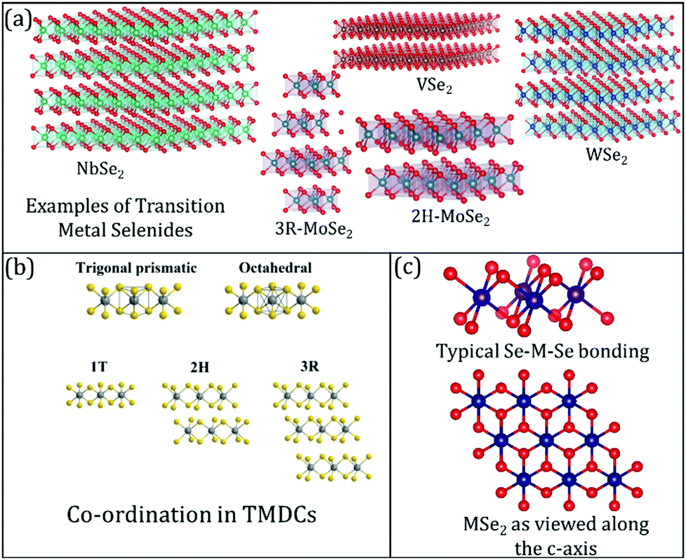 | ||
| Fig. 1 (a) Common examples of transition metal selenides used in lithium-ion batteries (LIB), sodium-ion batteries (NIB), and magnesium-ion batteries (MIB); (b) differences between the co-ordinations' geometries in TMDCs, in general. Reproduced with permission from ref. 7; (c) visualising the transition metal selenide bonding between the transition metal (M) and selenium (Se) along different axes. | ||
Transition metal sulfides (TMSs) and transition metal selenides (TMSe) are extensively investigated as promising electrode materials in energy storage systems.47,50,51 Although TMSes have similar properties to transition metal sulfides, we often notice that the volume energy density and rate capability of TMSes are comparatively higher than those of most of the transition metal sulfides due to the relatively higher density and electrical conductivity of selenium. Recently, TMSes have received much interest from researchers as promising electrode materials in electrochemical energy storage systems.52–54 A typical layered or sandwiched-like structure is always observed for these TMSes, where the metal atom and the selenium atoms are covalently bonded to each other (in the case of transition metal di-selenides, the metal atom stays in the center between two selenium atoms).55 Atoms in these three layers are covalently bonded, whereas the individual sheets are held by weak van der Waals forces. The latter force is weak enough to allow other atoms to reversibly intercalate in the inter-chain spaces, thereby forming intercalation compounds or intercalates; thus, the energy can be stored in the layered conductors.
In energy storage applications, layered TMSes are often hybridized with other materials, such as carbon, metal sulfides, metal oxides, and conducting polymers.56–62 Carbon finds usage as a composite with many-layered TMSes due to its high conductivity that accelerates electron transport in layered TMSe/carbon hybrids.63 Such behavior reduces the charge transfer resistance and improves the electrochemical performance. Besides possessing the advantages of individual components, layered TMSe-hybrids exhibit unexpected properties. For instance, the aggregation of TMDC nanosheets induced by van der Waals attraction can be effectively inhibited when hybridizing with other materials.64–73 Thus, the large surface area of TMDC nanosheets could be well maintained. In addition, other layered TMSes with intricate hierarchical structures or variable morphology can be synthesized by growing layered TMSes on substrates.74 This leads to excellent electrochemical performance in many systems.
Many widely researched TMSes have been applied in electrochemical energy storage because of their unique electrical properties.75–78 Compared to traditional graphite in lithium-ion batteries, transition metal selenides have a much higher theoretical capacity.68 Most of these TMSes can accommodate sodium and magnesium ions, in addition to lithium intercalation.79–82 TMSes also have good merits such as low cost, earth abundance, and convenience for fabrication, all of which greatly benefit their practical application in many electrical devices depending on the energy storage characteristics of TMSes.83,84 More importantly, these characteristics make them up-and-coming candidates for the electrodes of proposed electrochemical energy storage systems. Recently, many groups have highlighted their significant work and the impact of the applications of transition metal chalcogenides or modified-transition metal chalcogenides in energy conversion and storage.85 But, they often focus on sulfides more than selenides. This short review focuses on and highlights the fabrication of transition metal selenides, their challenges while being prepared by ambient pressure chemical vapor deposition (CVD), and the areas where they can be extensively explored. We systematically categorize their applications in electrochemical energy storage systems, including lithium-ion batteries, sodium-ion batteries, and magnesium-ion batteries.
Methods to prepare 2D layered transition metal selenides (TMSes)
The successful preparation of layered TMSes with high microstructural quality is crucial for their application in energy storage devices. During the past decade, various preparation methods have been developed to realize the morphology and structure-controlled synthesis of pure layered TMSe materials.86–91 Meanwhile, hybridization of layered TMSes with other materials, e.g., carbon materials, metal oxides, and metal sulfides, is also beneficial for their energy storage application due to the synergistic effect between the new materials and the composites. This signifies how the development of TMSes has been dramatically enriched by adopting one or more different techniques to enable significant tailoring of material properties in the past few years. The most commonly used techniques to prepare TMSes and their nanohybrids are the hydrothermal/solvothermal method, chemical vapor deposition (CVD), microwave irradiation, chemical bath deposition, ion-exchange, chemical exfoliation, etc.84,92–94 Here we only highlight the CVD-based routes (especially examples of ambient pressure CVD growth) for preparing TMSes and discuss their implementation in energy storage separately.Advantages of chemical vapor deposition (CVD) towards TMSe fabrication
As explained in the previous sections, 2D TMSes have many different atomic arrangements and electronic states. Each of these phases or polymorphs contributes to their catalytic or energy storage possibilities. 2H TMSes are characterized by trigonal prismatic coordination of metal atoms in each layer, and the individual layers are stacked in an ABAB order. 3R TMSes simply contain a shifted position of metal and chalcogen atoms, resulting in a different stacking order in their unit cell. On the other hand, metastable TMSes usually have an octahedral configuration of the metal atoms in an AA stacking mode. Sometimes, these 1T TMSes can distort into the 1T′ phase. Therefore, a meticulous synthesis route having proper phase-control in 2D TMSes is highly important. Among the different methods, chemical vapor deposition (CVD) is a very reliable synthesis route. CVD also provides a simple fabrication approach for high-quality variable-layer TMSes on suitably selected substrates. Therefore, monolayer TMSes with uniform film thickness can be easily synthesized using CVD. Issues with interface modification, such as phase/boundary modulation, are best realized in vapor deposition routes for 2D TMSes. Even, in-plane activation strategies can be rationally designed for many TMSe systems. So, up-scalable TMSe synthesis is possible by CVD.There are many examples of TMSe electrodes synthesized by CVD and used for energy storage applications. For example, Xiao et al. have reported the interlayer coupling in CVD-grown 2D MoSe2 flakes with screw dislocations on amorphous SiO2 substrates.95 They show how screw dislocations slightly widen the d spacing in MoSe2. They also attribute the weakened interlayer coupling to the presence of spirals that breaks the reflection and inversion symmetries of the lattices.95 Often scalability issues arise while trying to increase the yield of TMSes in the traditional CVD set-ups. So, proper precursor control and spatially uniform growth can be achieved using vertical CVD (VCVD). As an example, Lei et al. used VCVD to synthesize uniform TMSe monolayers by controlling the precursor concentration, gas flow, and temperature.96
Apart from direct-vapor assisted CVD synthesis on variable substrates, many complex TMSe nanostructures can also be synthesized. Such structural engineering will surely attract increasing attention for both fundamental studies and practical applications. Until now, hard-templating and self-template/template-free methods are some of the commonly researched areas for battery-grade TMSe synthesis.97 These can lead to complex structures having spherical, tubular, and polyhedral shapes, which are compatible with energy storage systems. In some of these cases, precursor modification is done in CVD, but we see very few reports which completely focus on TMSe fabrication starting with their growth and further modification in CVD.
Many in-plane variations and phase transformations can allow new accessible TMSe functionalities when prepared by CVD. Under suitable growth conditions, such TMSe modification can be achieved partially or entirely. The layer-by-layer variation can also be easily controlled in the TMSes when subjected to proper parameter control to understand their microstructural evolution and relations towards electrode preparation.
The reactivity of TMSes can be effectively modulated through interface engineering, which is of paramount importance in exploring the intrinsic activity of their in-plane atoms. The huge advancement in understanding reaction optimization, substrate choice, and precursor optimization have paved the way for modulating the electronic structure of TMSes by CVD-based routes, which include defect engineering, substitutional doping, and hybridization with different active functional species. In fact, based on the existing reports of TMSe for batteries, it can be assumed that the next-generation energy materials require further research based on TMSe surface and interface engineering in different CVD-based systems. Therefore, a proper insight into intermediate formation, growth and seeding strategies can be advantageous towards synthesizing the next generation layered TMSe battery materials.
Chemical vapor deposition (CVD)-based growth routes for synthesizing layered TMSes
Four common routes for TMSe growth using different CVD-based systems have been reported so far.98 They can be summarized as follows:Reports focusing on why ambient pressure CVD synthesis is favorable for layered TMSes
Different strategies have been applied within the CVD technique to obtain high quality, large-scale mono- and few-layer TMDCs to explore their promising properties in various fields of applications.98 Typically, all the CVD-based synthesis methods have been classified into “top-down” or “bottom-up” approaches. Generally, exfoliation methods are considered “top-down” while CVD is considered “bottom-up”.101–104 In a typical CVD process, precursors are reacted or decomposed and deposited as a mono- or few-layer film on the exposed substrate at relatively high temperatures. Many fundamental research experiments have been done to produce ultrathin TMDC materials with high crystal quality, scalable lateral dimensions, tunable thickness, and excellent electronic properties.As we see from the points mentioned in the previous section, CVD produces variable TMSe architectures and microstructures with high quality and precisely controlled layer numbers.100,105 This particular synthesis method is favorable for its simplicity, ease of TMSe preparation, efficient handling of elemental precursors, and precise control over defect-engineering or structure modification. Besides the planar SiO2/Si, graphite paper, and metal foil substrates, carbon cloths, graphene foams, and other homemade porous inorganic foams are often employed as templates to utilize their intrinsic porous structures to prepare electrodes with large surface areas.106–111 For example, Geng and co-workers prepared hierarchical 3D MoS2 nanosheet arrays by a CVD process using graphene-mediated Ni foam as a template.112 They first grew graphene on the Ni foam by CVD. This was treated with the molybdenum and sulfur vapors derived from the decomposition of tetrakis (diethylaminodithiocarbomato)molybdate(IV) (Mo(dedtc)4) at 400 °C in a tube furnace to form vertically aligned MoS2 nanosheet arrays on the surface of the graphene. Besides direct growth on substrates, 3D TMDC architectures can be transformed from 3D metal oxide structures by reacting with chalcogen vapors. In a recent study, vertical MoO2 nanosheet arrays were first grown on insulating SiO2/Si or conductive carbon cloth by a CVD process with MoO3 and H2.113 After calcination in Se vapor, vertical core–shell MoO2/MoSe2 nanosheet arrays were fabricated. Among all synthesis techniques, CVD is promising for synthesizing high-quality TMD layers with controllable layer number and domain size and excellent properties due to its simplicity and compatibility with industry standards. Compared with the chemical vapor transport (CVT) method, which is commonly used to synthesize bulk single-crystal materials, the typical CVD method, as discussed, is an efficient process to synthesize any mono- or few-layer TMDC, especially TMSes.114 For CVT-based growth, thermodynamic equilibrium is closely maintained by tuning the reaction temperature. The temperature ramp in CVT synthesis is generally slow which takes a few days to complete the reaction. A closed reaction vessel, such as quartz ampoules, sealed with the reactants under an inert atmosphere is generally used for CVT syntheses. In comparison, being kinetically driven, CVD processes are often faster than CVT to obtain few layers of material for structural studies and device applications. This makes CVD a preferred and reliable route to prepare high-quality two-dimensional (2D) TMSes. Typically, CVD-based growth of 2D TMSes involves activated chemical reactions of precursors in a specially designed environment. The precursors, conditions, atmosphere, substrates, and catalysts (if necessary) are several key factors affecting the final quality of 2D TMSs or TMSes.
CVD is also reliable for preparing TMCs@metal electrodes (where the TMC can be a TMS or TMSe) because of its simple setup and straightforward synthesis.115,116 This benefits the selenization or sulfurization process and helps with in situ reduction or doping processes. A figure highlighting the CVD method is presented in Fig. 2, showing a typical example of MoS2 grown on Au foil.117–119 The growth schematic is also shown in Fig. 2(e). The starting materials during the synthesis, such as chalcogen powder, precursors, and metal oxides, are packed into quartz boats, which are subsequently placed in the upstream heating zone center of a tube furnace. Simultaneously, the pre-treated metal substrate (typically cleaned or acid-washed) is placed in the downstream heating area of the furnace. During the experiment, the raw materials become gaseous in the upstream zone and move downstream with the gas flow.
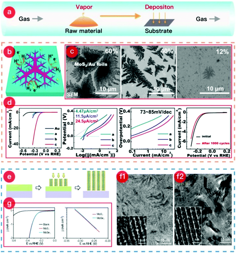 | ||
| Fig. 2 (a) Schematic of the CVD process. (b) Schematic of the dendritic MoS2@Au foil. (c) SEM images of each MoS2@Au sample with MoS2 coverages of 60%, 40%, and 12%, named a, b, and c, respectively. (d) Electrochemical performances of samples for HER. (The images of (b–d) were reproduced with permission. Copyright 2014, American Chemical Society, ref. 119.) (e) Schematic of the synthesis mechanism of MoS2@Mo or MoSe2@Mo. (f1) SEM image of the MoS2@Mo sample. (f2) SEM image of the MoSe2@Mo sample. (g) HER catalytic performance of both MoS2@Mo electrode and MoSe2@Mo electrode. (The images of (e–g) were reproduced with permission. Copyright 2013, American Chemical Society, ref. 117.) | ||
Meanwhile, the reaction between the raw material vapor and the substrate occurs at the desired temperature, and the product is deposited on the metal surface. After cooling to room temperature, a TMCs@metal self-supporting electrode is obtained. The facile growth method shows how a dendritic MoS2 monolayer on Au foil is easily formed via the CVD method. The scheme clearly illustrates the increased number of active sites on the edge of the dendritic MoS2 monolayer (see Fig. 2b). Furthermore, this study investigated the influence of the synthetic temperature on MoS2 coverage. As shown in Fig. 2c, temperatures of 880, 780, and 750 °C were applied during the growth of the dendritic MoS2 monolayer, which led to coverages of 60, 40, and 12%, respectively. Interestingly, the sample with the lowest coverage range (12%) exhibited the best catalytic performance and highest stability for the HER (Fig. 2d) due to the action of the macroscopically uniform, high-quality MoS2 monolayer.
In a similar fashion, Wu et al. have also synthesized MoSe2 on (100) oriented Au foils (as per Fig. 3), thereby producing highly crystalline MoSe2.120 The weak coupling between MoSe2 and Au surface is highly useful for direct transfer of the MoSe2 layers to other substrates (the quality of the layers being corroborated using Raman and STM techniques). Other examples of TMSe syntheses include ReSe2 synthesis on gold foils using ReO3 and Se powders, or ReO3 and Se powders being reduced and transferred on Si/SiO2 and sapphire substrates; ZrSe2 on sapphire; NbSe2 monolayers on Si/SiO2; ZnSe on Zn foil, etc.27,28,30,31,35
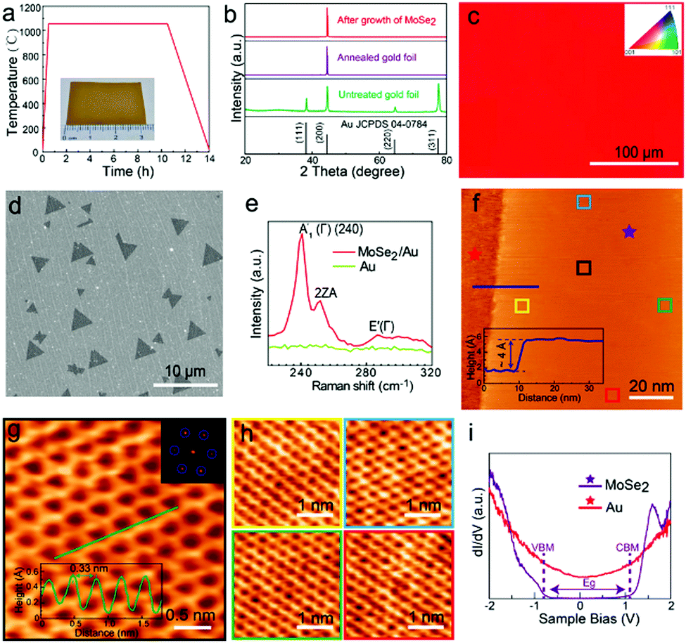 | ||
| Fig. 3 Substrate pre-treatment and characterization of monolayer MoSe2: (a) annealing pretreatment of Au foil. The inset shows Au foil after annealing; (b) XRD patterns of the Au foil before and after the annealing process; (c) EBSD image of a randomly selected position on the processed Au foil; (d) SEM image of triangular MoSe2 grown on Au foil by CVD; (e) Raman spectroscopy of the MoSe2 domain and the Au substrate; (f) large-scale STM image of MoSe2 with the bare Au substrate; the line profile across the substrate and MoSe2 is presented in the inset; the height of MoSe2 is around 4 Å; the sample bias is 0.5 V and the tunnel current is 1 nA; (g) atomically resolved STM image of a small MoSe2 domain with the honeycomb structure; the sample bias is 180 mV and the tunnel current is 200 pA. The FFT image shown in the inset shows the periodicity of MoSe2; the line profile of the lattice in the inset reveals that the lattice constant is around 0.33 nm; (h) atomic resolution images (sample bias 5 mV, tunnel current 1 nA) at different positions on the MoSe2 sheet marked by variable color squares in (f), demonstrating that the MoSe2 domain is defect-free at different positions and has a long-range high-quality crystalline structure; (i) dI/dV spectra of MoSe2 and the substrate obtained from red and purple stars in (f). (The images of (a–i) were reproduced with permission: copyright 2021, American Chemical Society, ref. 120.) | ||
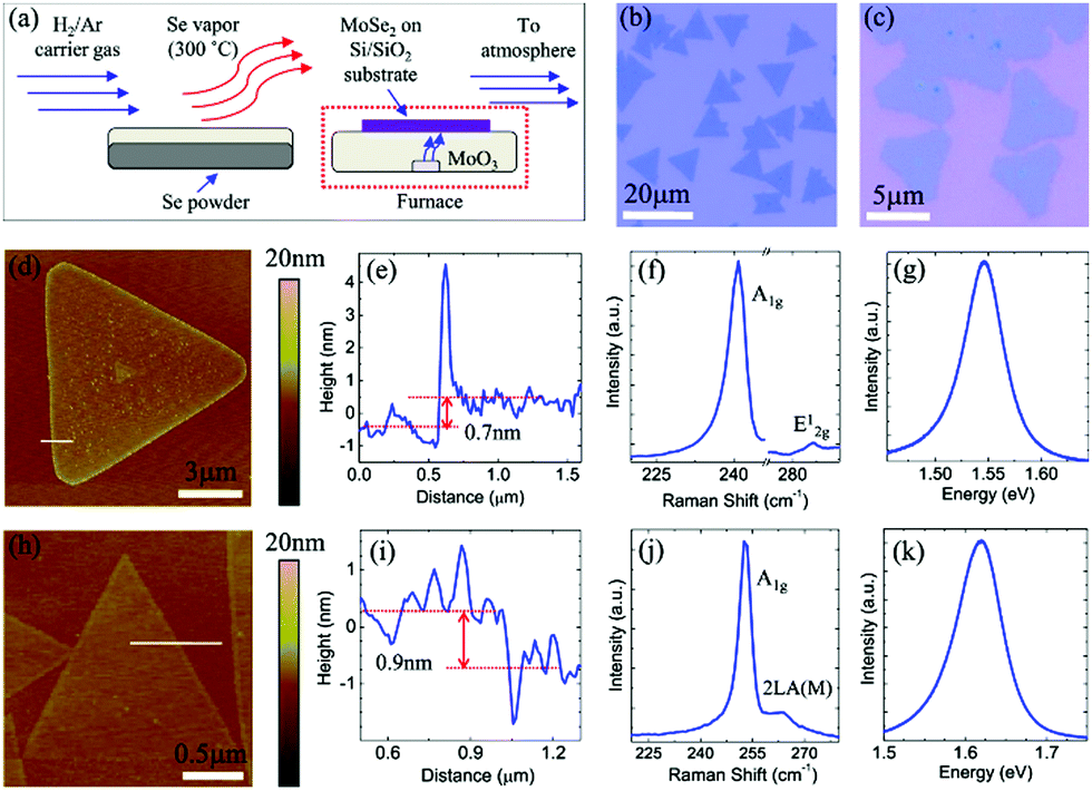
Previous reports also show how Se pellets and transition metal oxide powders such as molybdenum oxide (MoO3) powder have been used as precursors.121 When they are heated, and a clean Si wafer with a 275 nm SiO2 top layer is placed face down in the boat, they yield large MoSe2 triangular domains or films (as shown in Fig. 4(a)–(e)). In this case, H2 was used for reducing the MoO3 powder at 750 °C.121
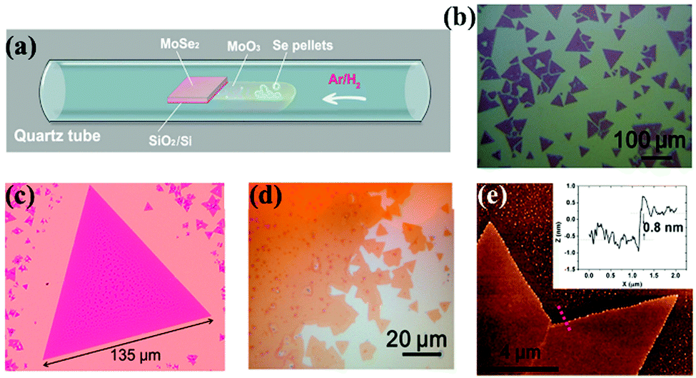 | ||
| Fig. 4 MoSe2 monolayer synthesis and morphology. (a) Schematic of the controlled synthesis of monolayer MoSe2via CVD. Se pellets and MoO3 powder are positioned in the same ceramic boat at the center of the tube furnace. (b–d) Typical optical images of monolayer triangles and continuous film. Small bilayer domains with darker color can be observed in (c) and (d). (e) AFM height topography of monolayer MoSe2, and the height profile (inset) showing a thickness of ∼0.8 nm, as measured along the red dotted line. (Image reproduced with permission from American Chemical Society, ref. 121.) | ||
There are reports of direct selenization of transition metal foils to obtain uniform and highly crystalline few-layered TMSes.33 MoSe2 on Mo foil is one of the best-known examples of TMSe growth. The material prepared by using such an approach by ambient pressure CVD has dimensions over the order of centimetres by directly selenizing annealed Mo foil surfaces in selenium (Se) vapor at 550 °C for 60 min under atmospheric pressure. After preparation, the obtained films are easily transferrable to various substrates by removing the Mo foil using a diluted ferric chloride (FeCl3) solution. The thickness of the thin films transferred onto a 285 nm SiO2/Si substrate is in the range of 3.4 to 6 nm (as detailed in Fig. 5(a)–(k)).
 | ||
| Fig. 5 (a) Schematic of the AP-CVD setup used for the growth of 2D TMDCs such as MoSe2. Optical microscopy images of (b) MoSe2 and (c) WSe2 monolayer domains grown on Si/SiO2. AFM image, height profile across the line marked on the AFM image, and Raman and PL spectra of (d–g) MoSe2 and (h–k) WSe2. (Figure reproduced from ref. 92.) | ||
Studies also focused on the importance of growth temperature and on how the metal/chalcogen flux in atmospheric pressure chemical vapor deposition influences the growth of MoSe2 and WSe2 on Si/SiO2 substrates.92 From scanning electron microscopy and atomic force microscopy, it was confirmed that the growth temperature and transition metal flux dictate the domain sizes and microstructures.92 The triangular or hexagonal domains further evolve into branched structures as the growth temperature (metal flux) is changed. The competition between adatom attachment to the domain edges and diffusion of adatoms along the domain boundary determines the evolution of the observed growth morphology. Depending on the growth temperature and flux, two different branched structures, fractals and dendrites, were reported during ambient pressure CVD growth.92
Apart from the elemental precursor or oxide precursor examples mentioned above, we also observe other materials such as elemental powders being used. But such transition metal powder precursors are used in CVT synthesis than in CVD synthesis. Also, selenization of as-deposited oxide or transition metal thin films in ambient pressure CVD is well-known.103 There are other reports based on the WSe2 platelet formation on W foil by using already synthesized WSe2 powder.122
Other than the TMSe preparation routes in the ambient pressure CVD which concentrate mostly on the small area domains of triangles or islands formed on the exposed surfaces of the substrates, there are also previous reports which highlight continuous TMSe film formation. For example, Malik et al. discuss in a related review how semiconducting TMSes and TMSs have been synthesized using various single source precursors by CVD.123 The synthesis procedure using such a method has been widely investigated to prepare defect-free and complex hetero-films of various TMSes and TMSs.110 But most of these syntheses use AACVD or MOCVD as their fundamental growth optimizing system. Additionally, evaporating oxide-based precursors on the substrate using MBE, or sputtering is also common for post-selenization treatments in AP-CVD.94
Factors influencing the growth and development of TMSes by ambient pressure CVD synthesis
As we understand from the previous section, there are several factors influencing the growth characteristics of various TMSes. The growth and microstructural evolution of TMSes synthesized by ambient pressure CVD depend on(a) type of precursors used in the synthesis,
(b) reaction temperatures and temperature gradients,
(c) substrates used for growth or deposition, and
(d) gases used for synthesis (and for post-treatments).
The factors mentioned above influence
(i) the number of layers of the TMSes formed,
(ii) the quality of the layers (i.e., if defects are present),
(iii) the domain sizes,
(iv) the ease of transfer of TMSe through mechanical or liquid-phase exfoliation.
Mechanistic insights and further examples of the microstructural fine-tuning of TMSes by ambient pressure CVD
The TMSe growth is directly correlated to their layers and lateral sizes. Generally, the fundamental premise for layer-by-layer growth from solid–gas reactions can follow any of the three widely known growth modes (Volmer–Webber, Frank Van-der Merwe, or Stranski–Krastanov), but an ideal highly crystalline TMSe growth should follow Frank–van der Merwe mode. Nevertheless, these growth modes can be properly verified if the substrate is only used for the deposition (such as TMSe deposition on Si, Si/SiO2, sapphire, etc.). In such reactions, the TMSe vapors deposit and form nanocrystals by random nucleation on the substrate surface. After nucleation, the gaseous sources tend to diffuse to the edges of the nuclei. The crystals show preferential growth along the lateral dimension of the nanocrystals, forming distinct nanosheet islands on the substrate surface. Such evolution on a prolonged reaction time can induce coalescence of adjacent nanosheets or layers into islands to produce continuous films. It is, therefore, necessary to develop a complete understanding of the seeding and growth profiles of the TMSe nanosheets. Perhaps the most critical factor in the usefulness of the gas-phase growth strategy is the orientation of the sheets on the substrate. TMSes can grow perpendicular (edge-maximizing) or parallel (epitaxial) to the substrate.125 TMSe films grown in these differing orientations exhibit vastly different properties. For many such recent examples, the deposited materials grow perpendicular to the surface of the substrate to minimize the energy penalty due to the interactions of the two surfaces, unless specific experimental parameters are chosen to reduce this effect and obtain laterally oriented nanosheets.116,125 In this situation, several conditions are required to promote the epitaxial growth of TMSe nanosheets on a substrate.There have been many other attempts to grow transition metal selenides using CVD. Zou's work reported that WSe2 and W(SexS1−x)2 nanoflakes on carbon nanofibers were synthesized by placing the Se and S powder upstream at a distance of approximately 20 cm from the furnace center, where the pre-prepared WO3 NPs were placed.126 Taking WSe2 as an example, as the furnace temperature increased to 1000 °C at 5 °C min−1, the Se vapor diffused and reduced the WO3 NPs on the surface, forming volatile sub-oxides WO3−x.126 The formed WO3−x were rapidly selenized into the WSe2 product for lateral growth or incorporation of WSe2 nanoflakes on the substrate. Through performing CVD experiments at different temperatures, Zou et al. synthesized metal selenide catalysts with other nanostructures, e.g., nanoplates at 880 °C, nanosheets at 940 °C, and microparticles at 980 °C.126 For fabricating the material of MoSe2, Se powder and MoO2 were separately placed in two ceramic boats and heated to a set temperature at a heating rate of 25 °C min−1 under mixed gas flow (Ar and H2). Changing the growth temperature changed the amount of Mo and Se vacancies in the following order: nanosheets > nanoplates > microparticles.127 In addition, it also gives further insight into doping or substitution strategies of different TMSes using CVD.
Considering all the examples mentioned in the previous sections, we believe that more unique approaches will be developed for the CVD-based synthesis of transition metal selenides. Most of the syntheses highlighted above show the nature of growth based on films deposited on dielectric substrates. In the next section, we discuss how transition metal foils can be a suitable substrate for few-layer to bulk growth of various TMSes.
Importance of ambient pressure CVD-based TMSe syntheses using transition metal foils as self-nucleating precursors
There are many studies focusing on the synthesis of TMDCs from transition metal (TM) foil.128–131 The existing literature indicates that a lot of research is still needed to understand the complex growth mechanisms when TMSes are synthesized directly from TM foil. We will describe here specific examples, with many illustrations taken from the research done in our lab.The Nessim group previously showed how TMCs form starting from the elemental foils and chalcogens as precursors.132 The photograph is shown in Fig. 6. A schematic of the setup is shown in Fig. 7. This two-furnace-based CVD setup is typically used as a part of many synthesis strategies (all operating at ambient pressure).133Fig. 7 also provides further examples of how we have successfully designed layered TMSes (rhenium selenide (ReSe2), tungsten selenide (2H-WSe2), niobium selenide (NbSe2), and molybdenum selenide (2H-MoSe2) using the AP-CVD approach. All the materials were upscaled starting from the respective transition metal foils (Re, W, Nb, and Mo), leading to few-layered growth, a significant yield, or an almost complete conversion of the metal precursors to the TMSe.
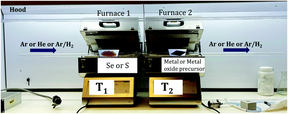 | ||
| Fig. 6 Furnace-based ambient-pressure chemical vapor deposition (AP-CVD) setup in the Nessim Lab. This system is composed of two furnaces in series. Digital mass-flow controllers (MFCs) for many gases, including Ar, forming gas, H2, C2H4, N2, etc., control gas flow. In the first furnace, we sublimate the chalcogen (S or Se) powder, while the reaction with the metal foil occurs in the second furnace. The two temperatures, T1 and T2, can be independently controlled. | ||
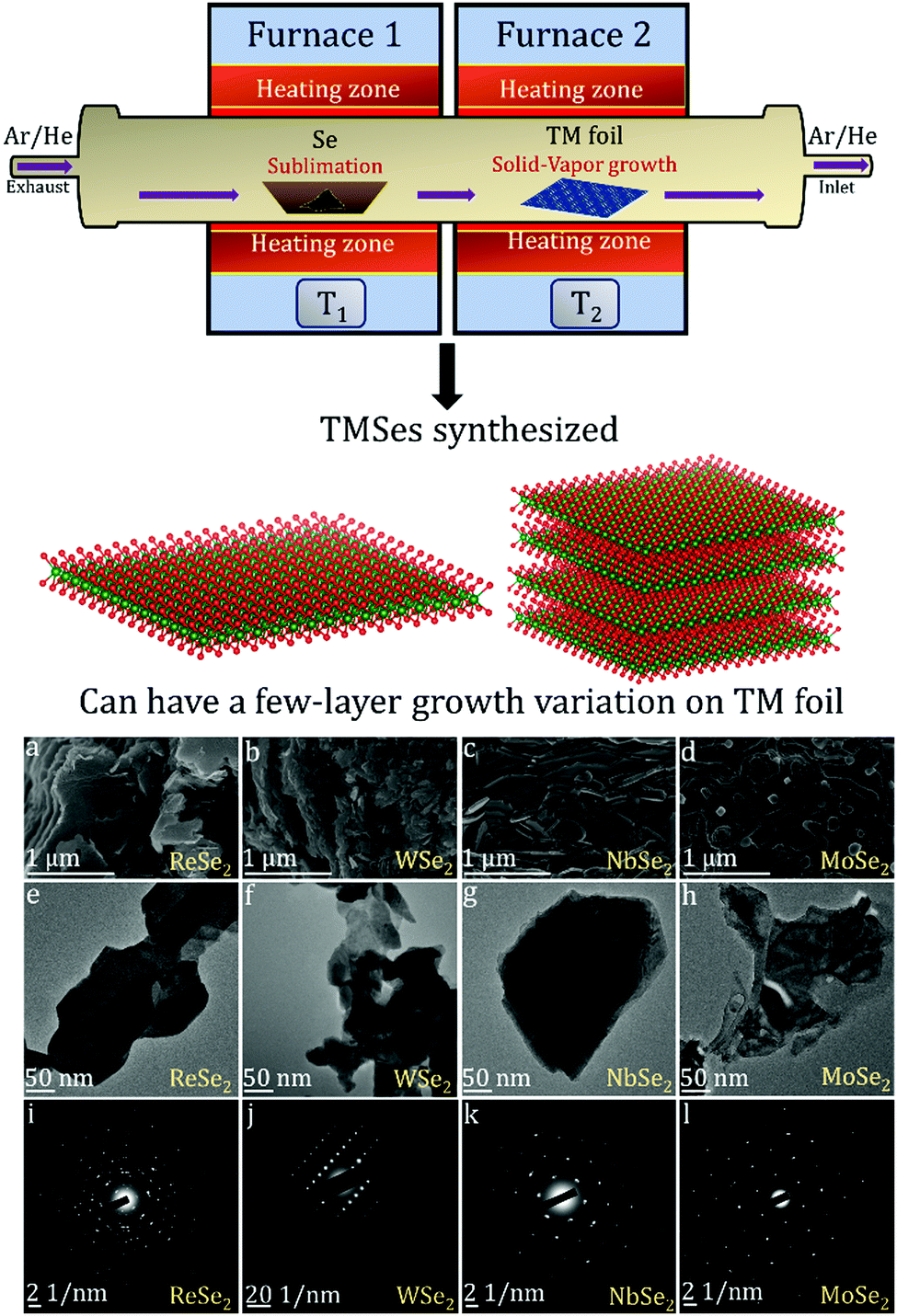 | ||
| Fig. 7 Schematic of the furnace with the direction of Se vapor flow in the setup as photographed in Fig. 6 (the setup was used to synthesize ReSe2, WSe2, NbSe2, and MoSe2 from the respective transition metal foils as per a previous solid–vapor CVD growth approach in the Nessim Lab). Fig. 6 shows the initiation of primary and secondary surface nucleation during CVD synthesis of layered TMSes on the transition metal foil depicted in blue. (a), (b), (c), and (d) denote high-resolution scanning electron microscopy (HRSEM) images of few-layered ReSe2, WSe2, NbSe2, and MoSe2; (e), (f), (g), and (h) denote low magnification transmission electron microscopy (TEM) images of ReSe2, WSe2, NbSe2, and MoSe2; (i), (j), (k), and (l) denote the selected area diffraction (SAED) pattern of ReSe2, WSe2, NbSe2, and MoSe2, indicating that they are of a single-phase. The bulk and exfoliated images are conclusive towards the layered morphology of TMSes being prepared by the ambient pressure CVD. Each material was thoroughly optimized with respect to reaction parameters to convert the transition metal foil to the corresponding TMSe fully. Therefore, such CVD-based reactions are highly scalable, providing a better yield of the layered TMSes. | ||
There are many reasons behind choosing the AP-CVD route for TMSe synthesis. Simplicity of initial precursors can be one of the major reasons as to why elemental precursors like TM foil and elemental Se are preferable. If only TM foil is used as the starting prototype for the synthesis, it eases the solid–vapor growth approach. In some cases, it can provide greater control over the total number of layers being grown on the foil. In other cases, the reaction can prove to be cumbersome and difficult to control if the desire is to obtain only a few-layers of the final TMSe. Such issues over number of layers formed can be solved by ideally fine-tuning the reaction parameters such as gas flow, amount of Se introduction, total reaction time, pre-annealing procedures, nature of gas used, and introduction of reducing agents or atmosphere.
We tried to find further examples in the literature for the discussion on the specific TMSes being synthesized directly on TM foil by AP-CVD. Based on our survey, we discuss the few existing reports concentrating on the TMSe syntheses from the corresponding transition metal (TM) foil using ambient pressure CVD.
We take as an example the synthesis of WSe2 using AP-CVD. Closer inspection for finding out references of the phase diagram for W and Se shows us that they are not available. Therefore, to understand the possible reactions between elemental Se and W precursors as a function of temperature, vapor pressure, reactants, gases, etc., we relied on previous reports based on the synthesis of this material. It was also reported that 2H-WSe2 could be prepared using solid-state mixing of WO3 powder with elemental Se. Other reported methods of WSe2 preparation include surface selenization of as-deposited tungsten oxide (WO3) powder on Au foils, or CVT-based growth on W foil, or halide-assisted growth of monolayer WSe2 crystals, etc.32,134,135
The growth of WSe2 nanowires on W foil is reported in the literature, using Se powder and N2 atmosphere but the reaction mechanism is not discussed in detail.136 Another work by Konar et al. indicates how AP-CVD can be used effectively to produce WSe2 layers on W foil.11 A specific temperature gradient of 250 °C between the two furnaces is vital throughout the reaction. It helps the vapor from the elemental Se to react and deposit on the surface of the W metal foil. The Se boat was immediately pulled out once the reaction was over, and the WSe2 sample was slowly cooled to room temperature. The effects in the final products due to change in the reaction parameters.11 The effects of optimization of carrier gas flow, total reaction time, Se precursor quantity, nature of inert carrier gas, surface acid-etching, reducing atmospheres, etc., are discussed in detail. These optimized reaction conditions prove that TMSes can be effectively synthesized with ease by AP-CVD using TM foil as the initial reactant. It also highlights that transition metals with otherwise higher activation energy can also be used to prepare different selenide polymorphs using this AP-CVD method and very simple precursors. The as-modified process parameters also confirmed the formation of the phase-pure material. Extensive characterization of the bulk and exfoliated material confirmed that 2H-WSe2 was layered. The growth of this material also highlights its exfoliable nature and the propensity towards homogenous dispersions when ultra-sonicated in low-boiling point solvents. In addition to the successful few-layered WSe2 development on the W foil, the microstructure can also be fine-tuned in terms of the layer number. For example, shorter reaction times within the range of 15–10 min produced few-layered growth of WSe2 thin film on the W foil. The exfoliated material from each reaction time (i.e., as collected from 15 min, 30 min, 45 min, 1 h, and 2 h) suggested the strong anisotropic behavior of the material as per the ex situ XRD measurements. The anisotropic line broadening is evident at all reaction times and can explain its structural defects. The underlying growth mechanisms were evaluated as a function of time, temperature, surface etching, and nature of the inert carrier gas used for the synthesis. The proposed growth mechanism in WSe2 show that the that the layers have evolved due to the close interaction between the Se vapor and the solid W foil surface. Such solid–vapor interaction formed various nucleation sites on the foil surface, leading to primary and secondary particles. The growth optimization also shed light on further experiments that eventually led to the W foil's total consumption, leading to the complete transformation of the elemental W precursor into the 2H-WSe2 powder. This shows promise in terms of scalability of TMSe synthesis by APCVD where the yields of the as-synthesized material are quite low.
Studies based on the post exfoliation characterization of the TMSe (in this case, 2H-WSe2) indicated that the individual layers can be easily separated using the liquid-phase exfoliation (LPE) technique. In LPE-assisted layer separation, the idea is to oversee if the 2D layered TMSe can be dispersed in a low-boiling-point solvent such as ethanol or isopropanol. For dispersing 2H-WSe2, both ethanol and isopropanol were identified as the most suitable solvents. The layered nature of the as-deposited flakes or nanosheets of 2H-WSe2 on the Si/SiO2 substrate confirmed the material's thickness and lateral dimensions (1.7 nm for bi-layered 2H-WSe2 with an average lateral size of about 2–8 μm) using atomic force microscopy (AFM) measurements.11 In-depth high-resolution transmission electron microscopy (HRTEM) measurements confirmed the average particle sizes and the point defects present in the exfoliated layers of 2H-WSe2.11
The literature based on the synthesis of 2H-WSe2 highlights that the material can be prone to surface oxidation. Previous reports on monolayer WSe2 (synthesized by a bottom-up approach) indicate that the single-layer 2H-WSe2 can easily be oxidized on air-induced protrusions at its edges.137 However, the oxidation with air exposure occurs mainly at step edges after the exposure of 2H-WSe2 to air for close to 9 weeks, and is less detected in the internal terraces. The oxidation of the step edges in WSe2 appears to be a self-terminating process. Since the studies combined bottom-up bulk synthesis of 2H-WSe2 (starting from the elemental precursors) with a top-down exfoliation method in ethanol and isopropanol as solvents, the effects of the ambient conditions toward the bulk 2H-WSe2 were also investigated.13 The bulk material showed no visible or morphological changes when exposed to air at room temperature (RT).11 This confirmed that the process is very suitable and prevents ambient oxidation of the material. To better understand the effect of surface oxidation, the effect of variation in the oxidation reaction parameters was studied, which revealed that the material is highly stable until 200 °C while annealing in the furnace in the presence of air.13
In a recent work on the AP-CVD synthesis of 2H-MoSe2 from the elemental Mo foil and Se powder, the underlying growth mechanism of the few-layered MoSe2 growing on the Mo foil surface (schematic of the synthesis and variable morphology of MoSe2 is shown in Fig. 8) is discussed.140 The effect of surface-etching leading to the formation of a variable morphology of the as-grown 2H-MoSe2 in a two-furnace system is also evident. The images of ex situ high-resolution scanning electron microscopy (HRSEM) indicate different assemblies of the as-grown 2H-MoSe2 nanosheets. An exhaustive refinement of reaction parameters showed a complete reaction of the transition metal foil with the elemental Se precursor leading to a precise arrangement in its overall flake organization as suggested by the layered formation of MoSe2 on the exposed Mo foil surface. The exfoliation parameter optimization also consolidates that the binding forces between the layers in each morphology are different. It yields a different number of layers (with a significant difference in the lateral dimensions of the nanosheets).
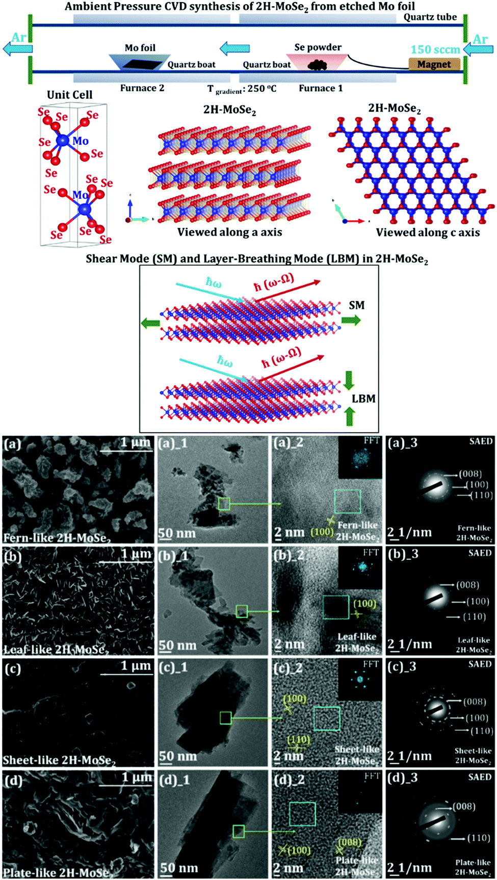 | ||
| Fig. 8 Schematic for ambient pressure CVD synthesis of 2H-MoSe2 starting from etched Mo foil and Se powder. The Mo foil is etched with different HCl strengths (giving rise to 4 different morphologies with varying strengths of HCl). Furnace 1 is set at 650 °C, and furnace 2 is set at 900 °C (maintaining a temperature gradient of 250 °C). 2 cm × 2 cm of Mo foil and 1.5 g of Se are shown in the schematic. The flow of Ar gas is set to 150 sccm. A ball and stick representation of the 2H variant of 2H-MoSe2 is demonstrated. The red balls indicate Se, and the blue balls show Mo in the unit cell drawn beside (where a = 3.288 Å and c = 12.91 Å). The structures are visualized along the a axis and the c axis. A representation of shear mode (SM) and layer breathing mode (LBM) of 2H-MoSe2 is also shown (reproduced with permission from ACS Omega); evolution in the morphology of 2H-MoSe2 concerning variable etching conditions using HCl (starting from etching of pristine Mo foil in (a) 0.0001 M (fern-like), (b) 0.001 M (leaf-like), (c) 0.01 M (sheet-like), and (d) 0.1 M (plate-like) HCl solutions). All the visible interlayer fringes are shown in each HRTEM image corresponding to the respective morphologies (reproduced with permission from ACS Omega, ref. 140). | ||
Study of structural parameters and defects in APCVD-synthesized TMSes
We still need to study structural parameter changes while using the ambient pressure CVD-based synthesis of TMSes. TMSes of the type MSe2 contain easily exfoliable layers (as explained before), resulting in essentially 2D materials. Planar structural defects, such as stacking faults (SFs), can effectively change the atomic arrangement.149 It influences electronic properties and makes these materials useful for various applications (optoelectronic devices, spintronics, gas sensing, catalysis, energy storage, thermoelectrics, etc.). Previous reports on TMDC synthesis with specific SFs highlight issues during synthesis. Such 2D defects must also be stable and consistent under experimental variations. The facile preparation of 2H-WSe2 on W foil by an ambient-pressure CVD resulted in inherent selenium vacancy formation during the synthesis. The 2D planar defects in these 2H-MSe2 systems were of intrinsic type-I.149The spontaneity with which the chalcogen will react often depends on chalcogen vapor pressure at different sublimation temperatures. For instance, both selenium and sulfur have similar behavior in their sublimation points.150 The reactions between transition metal precursor and elemental sulfur are reportedly more vigorous when compared to similar reactions with Se.151 In most cases, sulfur itself tends to be a reducing agent, and therefore in situ reduction of the transition metal oxide might not be necessary. There are several reports of preparing the TMSes by ambient-pressure CVD using a small quantity of S to react better between the precursors.152 The use of S as a promoter in the selenization process played an essential role. It partially reduced WO3 while keeping the WO3−x concentration low while leading to the formation of WSe2 layers.152 In such a case, it also forms defects such as screw-dislocations due to WO3 partial reduction modulation.152
Ambient-pressure CVD-synthesized TMSes for energy storage applications
Energy storage systems have gathered huge hype as one of the most promising alternative energy sources in the past few decades. Recently, lithium, sodium, and magnesium batteries have been highly sought after for abundant lithium reserves, sodium precursors, and magnesium's high specific volume capacity.153–156 Therefore, transition metal selenides play an essential part as lucrative electrode materials for energy storage. Some of their properties are shown in Fig. 9.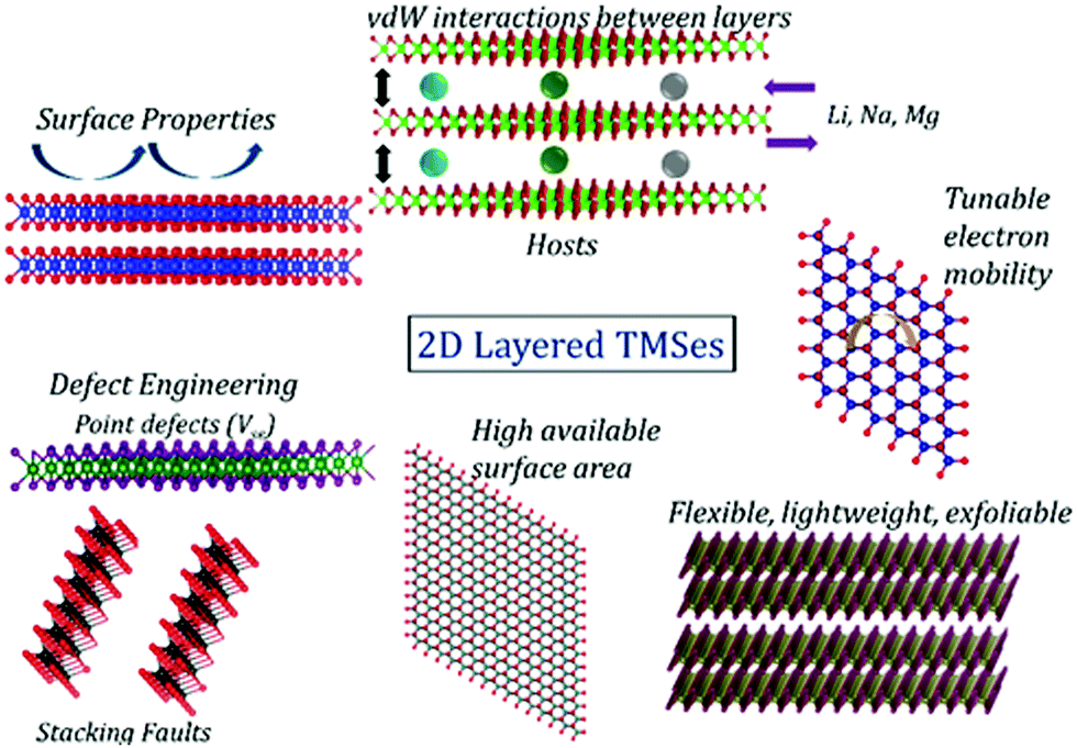 | ||
| Fig. 9 Properties of 2D materials that can effectively enhance the performance of energy storage applications. | ||
Although many reports are available in the literature regarding the energy storage capabilities of TMSes in LIBs, NIBs, and MIBs, most of these studies are focused solely on the materials prepared via the conventional hydrothermal or solvothermal, CVT, microwave-assisted, sonochemical, chemical bath deposition and other routes.45 Very few studies are based on applying ambient pressure CVD-synthesized TMSes towards energy storage.
As discussed before, the structures of many 2D materials and the presence of many different defects can play an essential role in introducing facile ion transport channels, leading to high ion conductivity in batteries.157,158 Such attributes support high current densities without any chemical and mechanical instability. In addition, the diffusion properties are enhanced, and ion mobility barriers for ultrafast ion transport are lowered due to their superionic conduction properties.157
Most of the studies on TMSes focus on understanding the underlying mechanisms towards reversible intercalation (in the case of LiB storage) and inducing a lesser degree of polyselenide formation (in the case of NIBs), a result of a decade-long optimization using solvothermal routes. Most of the syntheses include a pre-solvothermal step with an additional selenization route to post-process the microstructures. Therefore, much study is yet to be done using such layered selenides synthesized by the ambient pressure CVD.
Most of the materials discussed in the previous sections were synthesized entirely by the CVD using only elemental precursors. The optimization of the reaction parameters indicated that most of them could be wholly converted into bulk powder, which can then be pre-exfoliated and used in several energy storage systems.
Lithium-ion adsorption of TMDCs is a process of ion/electron transfer.157 The high concentrations of potential carriers, vacancies, and interstitials, and the low activation energies of ions hopping to the adjacent sides make the alkali metals have good conductivity in TMDCs. The exfoliable X–M–X layers in TMSes allow lithium/sodium/magnesium to be adsorbed and occupy vacant octahedral interstices in the hexagonal crystal lattice. The increased lithium concentration causes lattice distortion and strain, and even dislocations and lattice fragmentation, which provides diffusion channels for lithium ions to penetrate further into the TMDs material. Therefore, TMSes with tunable interlayer spacing enhance the lithium-ion capacity. However, it is worth noting that lattice strain can also cause cracks in the material and reduce the lifetime. It is also well known that defects weaken lattice strain in TMSes and improve lithium-ion adsorption behavior to some extent.159 For example, point defects in TMDCs help lower the migration barrier as the energy of the activated state is mainly determined by the electrostatic repulsion between the activated lithium-ion and its neighboring cations.160 Huang et al. predicted that the conductivity of the WS2/NbSe2 heterostructure is improved and the structure is more stable due to the new electronic states and large elastic constant, and the lithium diffusion barrier is as low as 0.18 eV.161
TMSes for SIB applications, such as MoSe2, have also gained increasing attention. For example, Ko et al. reported for the first time the synthesis of yolk–shell-structured MoSe2 microspheres by a facile selenization of the precursor for application as anode materials in SIBs.162 The synthesized yolk–shell morphology presented a flower-like structure, which, according to the authors, facilitated Na+ and electronic kinetics and assisted in the volume changes during charge and discharge cycles.162 Nevertheless, this also explains that the material was synthesized only partly using a combination of spray pyrolysis and CVD-based selenization. These MoSe2 microspheres showed 85% coulombic efficiency, with an initial charge capacity of 448 mA h g−1 at 200 mA g h−1.162 These reports based on MoSe2 studies during Na insertion processes highlight that CVD-synthesized layered MoSe2 must be studied in more detail.
The ongoing progress in nanostructured TMSes has a promising future in magnesium batteries by using such novel TMSes as electrode materials. Liu et al. recently constructed layered tungsten diselenide nanowires directly on tungsten foil and showed how the material works as a binder-free cathode in magnesium batteries.136 WSe2 nanowires exhibit efficient intercalation/de-intercalation activity toward Mg ions without evident morphology change.136 As shown in Fig. 10, the battery exhibited a reversible capacity of approximately 203 mAh g−1 at 50 mA g−1, whereas bulk WSe2 showed a relatively low capacity retention of 10% after 100 cycles. The electrodes had capacities of 142, 120, and 103 mA h g−1 at 800, 1500, and 3000 mA g−1, respectively, for 50 cycles. This is a clear indication of stable cycling and rate capacity. The CE of WSe2 nanowires was approximately 98.5% for 160 cycles.136 This points towards steady electrochemical behavior compared to the bulk having a CE of 93.8% for 50 cycles.
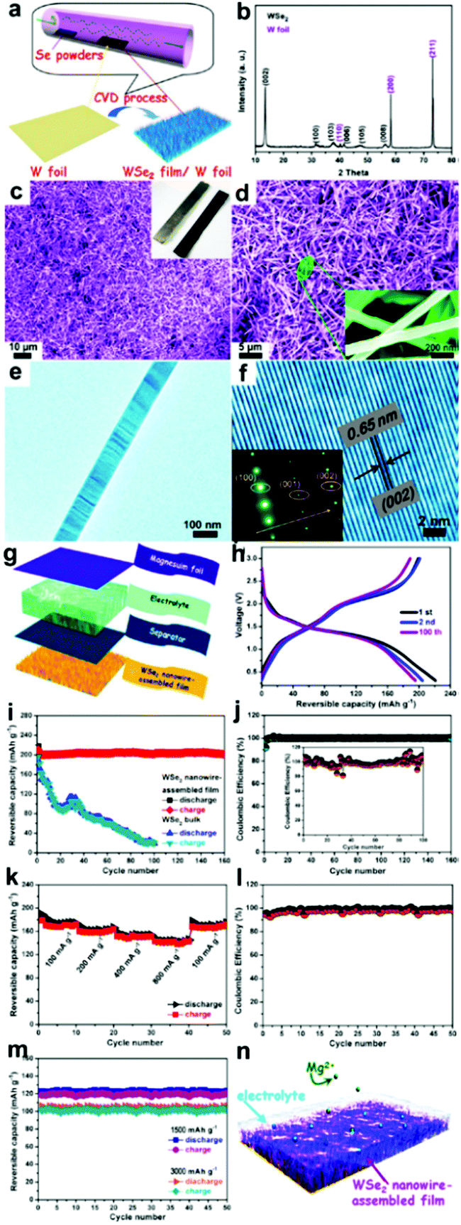 | ||
| Fig. 10 (i) Sample fabrication and morphological characterization of WSe2 nanowires grown on W foil. (a) Schematic illustration of the CVD procedures for the growth of the WSe2 nanowire film on W foil and its corresponding (b) XRD pattern, (c and d) SEM images, and (e and f) TEM images. The inset is the SAED pattern; electrochemical properties of the coin-type batteries measured at a current density of 50 mA g−1 between 0.3 and 3 V: (g) schematic representation of the as-assembled cell composed of magnesium foil anode, electrolyte, separator, and WSe2 film cathode, (h) charge/discharge curves, (i) cycling performance, and coulombic efficiency (CE); (j) rate-capability analysis of these electrodes. (k) Rate performance of the WSe2-based electrodes at various current densities. (l) The corresponding CE. (m) Long cycling performance of these electrodes at significant rates of 1500 and 3000 mA g−1. (n) Schematic of the operation principle of rechargeable magnesium-ion batteries based on WSe2 nanowire-assembled film. (Reproduced with permission from ACS Nano, 2013, ref. 136.) | ||
The TMSe fabrication using the precursor selenization process is not limited to MSe2 analogs. We also see reports on metal-rich TMSes such as copper selenide (Cu2Se) electrodes as explained before synthesized on a copper grid substrate tested as a promising material for sodium-ion batteries (as shown in Fig. 11).163 Cu2Se showed enhanced reversible capacities (about 250 mA h g−1), commendable cyclic stability, and low polarization.163 These findings corroborated Cu2Se as an encouraging cathode material for sodium-ion batteries.
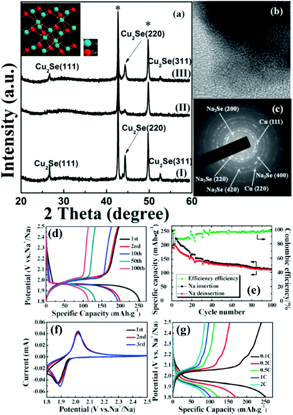 | ||
| Fig. 11 (a) Ex situ XRD pattern of the Cu2Se thin film at various states during the first cycle of the Cu2Se/Na cell with a voltage range of 1.8–2.5 V. (I) As-prepared; (II) after discharging to 1.8 V; and (III) after charging to 2.5 V. The crystal structure of Cu2Se is shown in the inset. (b) TEM image and (c) corresponding SAED pattern after discharging to 1.8 V; (d) typical charge–discharge voltage profiles of the initial 100 cycles of the Na/NaClO4/Cu2Se battery at a constant current rate of 0.1 C between 1.8 and 2.5 V; (e) cycling performance of the Na/NaClO4/Cu2Se battery cycled at 0.1 C between 1.8 and 2.5 V; (f) the initial three CV curves of the Na/NaClO4/Cu2Se cell between 1.8 V and 2.5 V versus Na+/Na at a scan rate of 0.1 mV s−1; (g) charge–discharge curves at various current densities (0.1 C, 0.2 C, 0.5 C, 1 C, and 2 C). (Figure reproduced with permission from Chem Comm. (RSC), ref. 163.) | ||
Regarding cyclability in as-purchased WSe2, Share et al. demonstrated this material as an electrode for the first time in NIBs (shown in Fig. 12).164 The WSe2 pristine electrode had a reversible capacity of 200 mA h g−1 at 20 mA g h−1.164 Other composites of WSe2, like carbon-coated WSe2, were further used by Zhang et al.165 In this study, tungsten and selenium, in their powder forms, were firstly ground by mechanical milling and subsequently annealed with carbon black. Afterwards, WSe2/C was directly used on the electrode. WSe2/C nanomaterials exhibited a discharge capacity of 467 mA h g−1 at 200 mA g h−1 current density, owing to the buffering of the carbon matrix and enhanced electronic conductivity of the composites.165
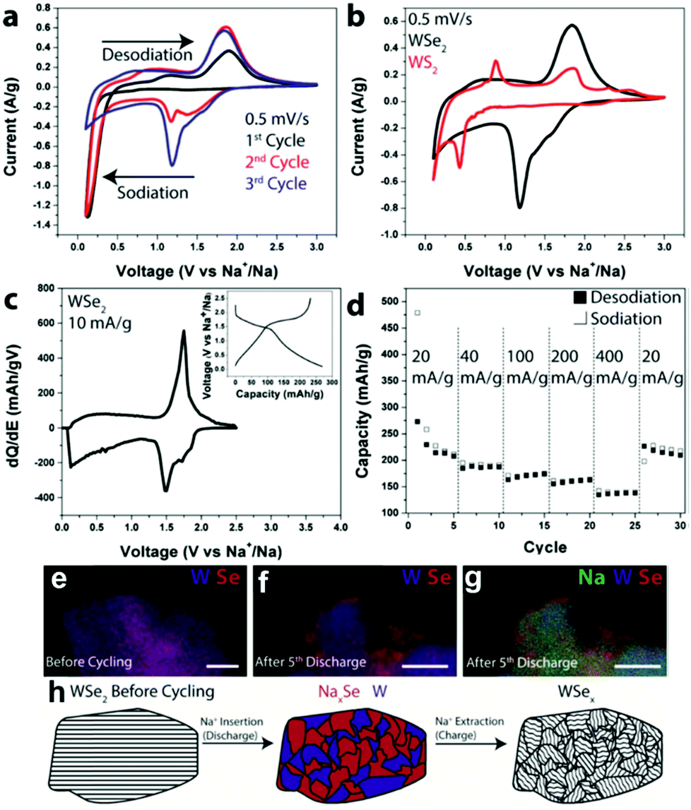 | ||
Fig. 12 (a) CV scans for the first three cycles from WSe2 devices with CMC and EC/DEC. (b) CV scans comparing the energetics of chemical storage in WSe2 and WS2 during the 3rd cycle. (c) dQ/dE of a WSe2 electrode at 10 mA g−1; inset: charge–discharge curves at 10 mA g−1. (d) Galvanostatic rate study at 20, 40, 100, 200, and 400 mA g−1. (e) EDS composite map of a WSe2 electrode before cycling; scale bar  100 nm. (f) EDS composite map of a WSe2 battery electrode after the 5th discharge showing W and Se; scale bar 100 nm. (f) EDS composite map of a WSe2 battery electrode after the 5th discharge showing W and Se; scale bar  100 nm. (g) The same EDS spectrum as (f) but with Na added. (h) Schematic illustrating the storage mechanism of Na in WSe2. Upon Na+ insertion, segregated domains of NaxSe and W form. After Na+ has been removed, WSe2 is reformed, but it is less crystalline than in its original state. (Figure reproduced with permission from RSC Advances, ref. 164.) 100 nm. (g) The same EDS spectrum as (f) but with Na added. (h) Schematic illustrating the storage mechanism of Na in WSe2. Upon Na+ insertion, segregated domains of NaxSe and W form. After Na+ has been removed, WSe2 is reformed, but it is less crystalline than in its original state. (Figure reproduced with permission from RSC Advances, ref. 164.) | ||
As described in the sections above, the previous work by Konar et al. deals with understanding the physico-chemical properties while synthesizing 2H-WSe2 by ambient pressure CVD from elemental precursors without any reducing agent.11 It deals with the issues of scalability of the final materials by a thorough parameter optimization process. The final as-synthesized TMSe shows appreciable performance when used as a LIB anode material.11 An elaboration on the redox processes of lithium-ion batteries (LIBs) indicates capacity increase up to 500 cycles. The discharge capacity up to the 50th cycle at 250 mA g h−1 of the material shows a stable value of 550 mA h g−1 on prolonged cycling. The material showed a capacity of ∼300 mA h g−1 when the current density was increased to 500 mA g h−1 after ∼750 cycles at 250 mA g h−1. After additional 500 cycles (total of 1200+ cycles) at 500 mA g h−1, a capacity of 271 mA h g−1 with a retention of ∼91% was recorded. These results for 2H-WSe2 indicate that the material's prime rate and stable cycling performance in its pristine form can be attributed to its layered 2D microstructure (Fig. 13). This can pave the possibilities towards high energy-efficient devices. Moreover, in a recent work, the functionality of CVD-synthesized layered 2H-WSe2 as an unconventional 2D coating material is also proven towards stabilizing high-voltage LIB-based cathodes (NCM and LNMO).166
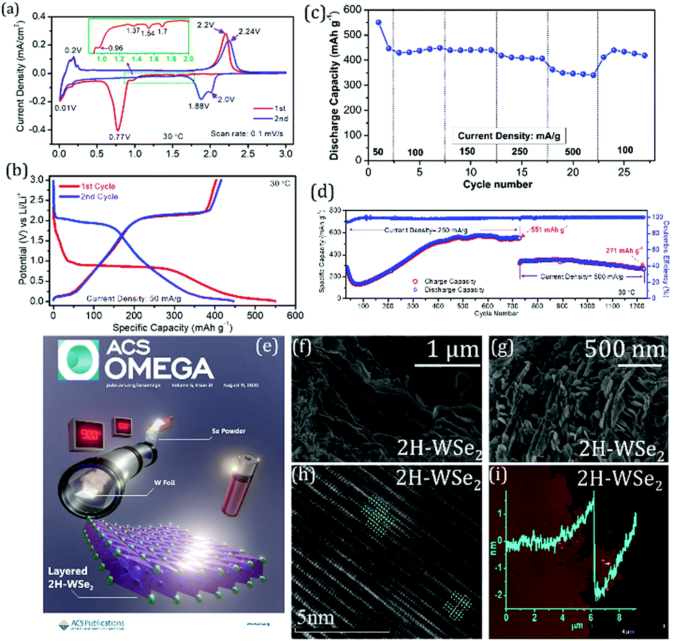 | ||
| Fig. 13 (a) Cyclic voltammograms for the first two cycles of 2H-WSe2vs. Li at a scan rate of 0.1 mV s−1 over a potential window of 0.01–3.0 V. (b) Galvanostatic voltage profiles for the first two cycles of WSe2 in a half-cell recorded at a current density of 50 mA g h−1. (c) Variation of the discharge capacity as a function of the applied current density measured using 2H-WSe2vs. Li half-cell. (d) Prolonged electrochemical cycling performance of the 2H-WSe2 electrode in half coin cell configuration (vs. Li/Li+). After the initial 27 cycles of rate performance, the cells were subjected to long-term cycling for 700 cycles at 250 mA h g−1 and another 500 cycles at 500 mA h g−1. (e) Schematic depicting a facile and straightforward approach towards bulk 2H-WSe2 synthesis by ambient pressure CVD for LiBs. (f and g) High-resolution scanning electron microscopy (HRSEM) images of 2H-WSe2; (h) high-resolution transmission electron microscopy (HRTEM) image of 2H-WSe2; (i) atomic force microscopy (AFM) measurement of the 2H-WSe2 drop-cast flake showing a thickness of about 1.8 ± 0.3 nm. (Figure a–g reproduced with permission from ACS Omega, ref. 11; figure h and i reproduced from Materials Characterization, Elsevier, ref. 149.) | ||
In a recent work, Yang et al. demonstrate the facile and highly scalable preparation of ZnSe@Zn metal foil being used as an anode in Zn aqueous batteries.33 The work demonstrates a high Zn utilization of 99.2% and an elongated cycle life of 1530 h during repetitive Zn plating/stripping. Under harsh experimental conditions (30.0 mA cm−2/10.0 mA h cm−2), it can still sustain to operate as long as 172 h, outperforming the state-of-the-art anode counterparts.33 Impressively, such layered ZnSe formation on the Zn foil anode can act as a cultivator to guide the preferential growth of the Zn(002) plane at the infancy stage of cycling.33
Additionally, we provide a table summarizing all the literature mentioning transition metal selenides being researched so far for their energy storage capabilities, which were synthesized or structurally modified by CVD (Table 1). Other reports of TMSes (synthesized mostly by hydrothermal routes) for energy storage are discussed in a recent review which shows the challenges and progress in using transition metal selenides to electrochemically store Na+ and K+.52
| Transition metal selenides | Morphology | Application | Rate capability (m a h g−1) | Ref. |
|---|---|---|---|---|
| WSe2 NWs on W foil | Nanowires | MIB | 103/3000 | 136 |
| Cu2Se on Cu grids | Thin film | NIB | 250 | 163 |
| WSe2 | Exfoliated powder | NIB | 200 | 164 |
| WSe2 from W foil | Nanosheets after exfoliation | LIB | 550 | 11 |
| MoSe2 from MoO3 | Yolk shell modified by CVD | NIB | 527 | 162 |
| MOF-derived SnSe nano-platelets in nitrogen-doped graphene cages | Combined steps of thermal selenization of Sn-MOF and direct plasma-enhanced chemical vapor deposition (PECVD) wrapping of the NG shell | NIB | 650 | 167 |
Conclusion and future perspectives
The recent literature shows how the conventional materials for energy storage, such as in LIBs, have evolved greatly in terms of their energy density, cyclability, cost, and safety since their invention and commercialization. Their success is immeasurable in terms of applicability towards flexible electronics and electric vehicles. However, much research is required for the current commercial LIBs to meet all the demands for performance, cost-effectiveness, and upscaling. The natural availability of lithium, cobalt, and nickel can be challenging for LIBs. Nevertheless, such imposed restrictions motivate future research on alternative chemistries for the next-generation batteries.168Other multivalent batteries (such as NIBs, MIBs) seem to be different but often share similar scientific/operating principles, which can be understood using similar characterization approaches. Huge efforts have been dedicated to understand the electrochemical mechanism of storing, say for example, Na+ or Mg2=, towards understanding the electrochemical reactivity/storage phenomena in TMSes. Sometimes contradictory ion-storage processes are also reported in the literature of TMSes, but it simply indicates that the conversion processes need to be studied in further detail for the NIBs or MIBs. The shuttle effect of intermediate polyselenides, effect of electrolyte composition, and full-cell investigations are required to facilitate cost-effective strategies for designing TMSe-based electrodes compatible with the energy storage systems. Among all the energy storage systems discussed here, we must mention that MIBs provide higher energy densities with minimum dendritic growth in the TMSe based electrodes. This can facilitate solid-state mobility without compromising the voltage and capacity.
Therefore, there are certain factors which will determine the commercialization of TMSes towards appropriate energy-storage settings. An optimization of these factors in the fabrication process of electrodes will help achieve the realistic goal towards fabricating Se-based batteries by CVD. Such deciding factors include
(a) A gradual increase of TMSe mass loading will ease the transfer of materials/technology towards future commercialization;
(b) Fabrication of safe TMSe active materials that minimize thermal runway during electrochemical ion storage;
(c) Develop new high-voltage (HV) cathodes or hetero-composites of TMSe and existing HV cathodes to mitigate instability issues towards the commonly used electrolytes in such energy storage systems.
From the CVD-based TMSe engineering perspective, the recent research in such materials focuses on synthesizing them through many approaches, where AP-CVD remains the least explored technique. We mostly observe the post-annealing or selenization of the precursors (sometimes prepared using a different route) in ambient pressure CVD. The APCVD-based process remains limited in usage towards TMSe fabrication for batteries. Few-layered TMSe films have recently shown great potential in energy storage devices. However, further research is required to improve and understand APCVD's mechanisms, material characteristics, and modification of the fabrication process. The scalability of TMSe yield through APCVD remains a major factor. Optimizing reaction parameters and precursors’ fine-tuning will ensure better insight into the synthesis of 2D TMSes on a large scale. Better experimental design of many such 2D layered TMSes using CVD can better corroborate the defect-nature, large-area flakes, etc., for practical applications in energy storage. In addition, surface structure, material strain, and surface charge are critical, and a variety of growth substrates or other precursors must be examined. In such cases, precursor adsorption, nucleation, domain sizes, substrate orientation, and growth direction also need to be studied in detail. Furthermore, reproducibility, uniform property distribution, and upscaling remain challenging issues that need to be addressed through research. We strongly believe that a simple APCVD-based fabrication approach can provide better tuning of physico-chemical properties, leading to better batteries in the near future.
Conflicts of interest
The authors have no conflicts to declare.Acknowledgements
RK and GDN are thankful to the Israel Science Foundation and Israel Prime Ministry Office for the alternatives initiative for partial funding of this study under the Israel Research Center for Electrochemical Propulsion (INREP) (Grant: ISF 2797/11) and Israel Ministry of Science and Technology (M.O.S.T.) Optoelectronics Grant (205509), titled “Compact monolithic wavelength-tuneable microcavity diode laser based on electro-optic phase modulation using 2D nanomaterial thin films,” for partially funding this study.References
- P. Das, Q. Fu, X. Bao and Z.-S. Wu, J. Mater. Chem. A, 2018, 6, 21747–21784 RSC.
- R. Rojaee and R. Shahbazian-Yassar, ACS Nano, 2020, 14, 2628–2658 CrossRef CAS PubMed.
- N. Deng, Y. Feng, G. Wang, X. Wang, L. Wang, Q. Li, L. Zhang, W. Kang, B. Cheng and Y. Liu, Chem. Eng. J., 2020, 401, 125976 CrossRef CAS.
- Z. Ali, M. Asif, T. Zhang, X. Huang and Y. Hou, Small, 2019, 15, 1901995 CrossRef PubMed.
- A. K. Geim and K. S. Novoselov, Nat. Mater., 2007, 6, 183–191 CrossRef CAS PubMed.
- Z. Wu, J. Qi, W. Wang, Z. Zeng and Q. He, J. Mater. Chem. A, 2021, 9, 18793–18817 RSC.
- Á. Coogan and Y. K. Gun’ko, Mater. Adv., 2021, 2, 146–164 RSC.
- Y. Wang, L. Zhou, M. Zhong, Y. Liu, S. Xiao and J. He, Nano Res., 2022, 15, 3675–3694 CrossRef.
- H. Ma, K. Huang, R. Wu, Z. Zhang, J. Li, B. Zhao, C. Dai, Z. Huang, H. Zhang, X. Yang, B. Li, Y. Liu, X. Duan and X. Duan, InfoMat, 2021, 3, 222–228 CrossRef CAS.
- J. Pang, Y. Wang, X. Yang, L. Zhang, Y. Li, Y. Zhang, J. Yang, F. Yang, X. Wang, G. Cuniberti, H. Liu and M. H. Rümmeli, Mater. Adv., 2022, 3, 1497–1505 RSC.
- R. Konar, R. S. Rosy, I. Perelshtein, E. Teblum, M. Telkhozhayeva, M. Tkachev, J. J. Richter, E. Cattaruzza, A. Pietropolli Charmet, P. Stoppa, M. Noked and G. D. Nessim, ACS Omega, 2020, 5, 19409–19421 CrossRef CAS PubMed.
- R. Konar, S. Das, E. Teblum, A. Modak, I. Perelshtein, J. J. Richter, A. Schechter and G. D. Nessim, Electrochim. Acta, 2021, 370, 137709 CrossRef CAS.
- A. Moumen, R. Konar, D. Zappa, E. Teblum, I. Perelshtein, R. Lavi, S. Ruthstein, G. D. Nessim and E. Comini, ACS Appl. Mater. Interfaces, 2021, 13, 4316–4329 CrossRef CAS PubMed.
- A. Eftekhari, Appl. Mater. Today, 2017, 8, 1–17 CrossRef.
- Y. Wang, J. Pang, Q. Cheng, L. Han, Y. Li, X. Meng, B. Ibarlucea, H. Zhao, F. Yang, H. Liu, H. Liu, W. Zhou, X. Wang, M. H. Rummeli, Y. Zhang and G. Cuniberti, Nano-Micro Lett., 2021, 13, 143 CrossRef CAS PubMed.
- W. Qian, S. Xu, X. Zhang, C. Li, W. Yang, C. R. Bowen and Y. Yang, Nano-Micro Lett., 2021, 13, 156 CrossRef CAS PubMed.
- M. Wu, Y. Xiao, Y. Zeng, Y. Zhou, X. Zeng, L. Zhang and W. Liao, InfoMat, 2021, 3, 362–396 CrossRef CAS.
- A. K. Thakur, M. Majumder, S. P. Patole, K. Zaghib and M. V. Reddy, Mater. Adv., 2021, 2, 2457–2482 RSC.
- A. Jetybayeva, B. Uzakbaiuly, A. Mukanova, S. T. Myung and Z. Bakenov, J. Mater. Chem. A, 2021, 9, 15140–15178 RSC.
- B. An, Y. Ma, G. Zhang, C. You and Y. Zhang, RSC Adv., 2020, 10, 42157–42163 RSC.
- T. J. Dai, Y. C. Liu, X. D. Fan, X. Z. Liu, D. Xie and Y. R. Li, Nanophotonics, 2018, 7, 1959–1969 CAS.
- A. T. Hoang, K. Qu, X. Chen and J.-H. Ahn, Nanoscale, 2021, 13, 615–633 RSC.
- Z. Zhou, T. Xu, C. Zhang, S. Li, J. Xu, L. Sun and L. Gao, Nano Res., 2021, 14, 1704–1710 CrossRef CAS.
- Q. Cheng, J. Pang, D. Sun, J. Wang, S. Zhang, F. Liu, Y. Chen, R. Yang, N. Liang, X. Lu, Y. Ji, J. Wang, C. Zhang, Y. Sang, H. Liu and W. Zhou, InfoMat, 2020, 2, 656–697 CrossRef CAS.
- R. Puttaswamy, N. S. Kotrappanavar and D. Ghosh, Mater. Adv., 2021, 2, 5006–5046 RSC.
- J. Chen, Y. Luo, W. Zhang, Y. Qiao, X. Cao, X. Xie, H. Zhou, A. Pan and S. Liang, Nano-Micro Lett., 2020, 12, 171 CrossRef CAS PubMed.
- M. Hafeez, L. Gan, H. Li, Y. Ma and T. Zhai, Adv. Mater., 2016, 28, 8296–8301 CrossRef CAS PubMed.
- H. Wang, X. Huang, J. Lin, J. Cui, Y. Chen, C. Zhu, F. Liu, Q. Zeng, J. Zhou, P. Yu, X. Wang, H. He, S. H. Tsang, W. Gao, K. Suenaga, F. Ma, C. Yang, L. Lu, T. Yu, E. H.-T. Teo, G. Liu and Z. Liu, Nat. Commun., 2017, 8, 394 CrossRef PubMed.
- L. Xing, X. Yan, J. Zheng, G. Xu, Z. Lu, L. Liu, J. Wang, P. Wang, X. Pan and L. Jiao, InfoMat, 2019, 1, 552–558 CrossRef CAS.
- S. Jiang, Z. Zhang, N. Zhang, Y. Huan, Y. Gong, M. Sun, J. Shi, C. Xie, P. Yang, Q. Fang, H. Li, L. Tong, D. Xie, L. Gu, P. Liu and Y. Zhang, Nano Res., 2018, 11, 1787–1797 CrossRef CAS.
- S. Jiang, M. Hong, W. Wei, L. Zhao, N. Zhang, Z. Zhang, P. Yang, N. Gao, X. Zhou, C. Xie, J. Shi, Y. Huan, L. Tong, J. Zhao, Q. Zhang, Q. Fu and Y. Zhang, Commun. Chem., 2018, 1, 17 CrossRef.
- J. M. Velazquez, F. H. Saadi, A. P. Pieterick, J. M. Spurgeon, M. P. Soriaga, B. S. Brunschwig and N. S. Lewis, J. Electroanal. Chem., 2014, 716, 45–48 CrossRef CAS.
- X. Yang, C. Li, Z. Sun, S. Yang, Z. Shi, R. Huang, B. Liu, S. Li, Y. Wu, M. Wang, Y. Su, S. Dou and J. Sun, Adv. Mater., 2021, 33, 2105951 CrossRef CAS PubMed.
- B. Silva, J. Rodrigues, B. Sompalle, C. Da Liao, N. Nicoara, J. Borme, F. Cerqueira, M. Claro, S. Sadewasser, P. Alpuim and A. Capasso, Nanomaterials, 2021, 11, 1–18 Search PubMed.
- Y. Tian, M. Zheng, Y. Cheng, Z. Yin, J. Jiang, G. Wang, J. Chen, X. Li, J. Qi and X. Zhang, J. Mater. Chem. C, 2021, 9, 13954–13962 RSC.
- L. H. Yao, W. Q. Cao, J. C. Shu, M. S. Cao and X. Di Sun, Chem. Eng. J., 2021, 413, 127428 CrossRef CAS.
- Z. Ali, T. Zhang, M. Asif, L. Zhao, Y. Yu and Y. Hou, Mater. Today, 2020, 35, 131–167 CrossRef CAS.
- R. Jin, C. Ren, H. Kang, S. Gao and S. Chen, J. Colloid Interface Sci., 2021, 590, 219–225 CrossRef CAS PubMed.
- D. Zhou, L. Zhao and B. Li, J. Energy Chem., 2021, 62, 27–42 CrossRef.
- Z. Ju, X. Zhang, J. Wu and G. Yu, Nano Res., 2021, 14, 3562–3575 CrossRef CAS.
- N. Liu, L. Chang, J. Wu, J. Fang and X. Xiao, Micromachines, 2021, 12, 1–17 Search PubMed.
- J. Y. Oh, J. H. Lee, S. W. Han, S. S. Chae, E. J. Bae, Y. H. Kang, W. J. Choi, S. Y. Cho, J.-O. Lee, H. K. Baik and T. Il Lee, Energy Environ. Sci., 2016, 9, 1696–1705 RSC.
- L. Zhang, Y. Lei, D. Zhou, C. Xiong, Z. Jiang, X. Li, H. Shang, Y. Zhao, W. Chen and B. Zhang, Nano Res., 2022, 15, 2895–2904 CrossRef CAS.
- B. Zheng, D. Li, C. Zhu, J. Lan, X. Sun, W. Zheng, H. Liu, X. Zhang, X. Zhu, Y. Feng, T. Xu, L. Sun, G. Xu, X. Wang, C. Ma and A. Pan, InfoMat, 2020, 2, 752–760 CrossRef CAS.
- D. M. Soares, S. Mukherjee and G. Singh, Chem. – Eur. J., 2020, 26, 6320–6341 CrossRef CAS PubMed.
- A. Eftekhari, J. Mater. Chem. A, 2017, 5, 18299–18325 RSC.
- Z. Hu, Z. Wu, C. Han, J. He, Z. Ni and W. Chen, Chem. Soc. Rev., 2018, 47, 3100–3128 RSC.
- S. Zhang, J. Pang, Q. Cheng, F. Yang, Y. Chen, Y. Liu, Y. Li, T. Gemming, X. Liu, B. Ibarlucea, J. Yang, H. Liu, W. Zhou, G. Cuniberti and M. H. Rümmeli, InfoMat, 2021, 3, 1455–1469 CrossRef CAS.
- M. S. Sokolikova, P. C. Sherrell, P. Palczynski, V. L. Bemmer and C. Mattevi, Nat. Commun., 2019, 10, 712 CrossRef CAS PubMed.
- C. Wu, G. Zhao, X. Yu, C. Liu, P. Lyu, G. Maurin, S. Le, K. Sun and N. Zhang, Chem. Eng. J., 2021, 412, 128736 CrossRef CAS.
- N. Bisht, P. Phalswal and P. K. Khanna, Mater. Adv., 2022, 3, 1415–1431 RSC.
- Y. Lu, A. P.-V. K. Saroja, R. Wei and Y. Xu, Cell Rep. Phys. Sci., 2021, 2, 100555 CrossRef CAS.
- X. Wei, C. Tang, Q. An, M. Yan, X. Wang, P. Hu, X. Cai and L. Mai, Nano Res., 2017, 10, 3202–3211 CrossRef CAS.
- Y. Zhu, L. Peng, Z. Fang, C. Yan, X. Zhang and G. Yu, Adv. Mater., 2018, 30, 1706347 CrossRef PubMed.
- H.-J. Li, K. Xi, W. Wang, S. Liu, G.-R. Li and X.-P. Gao, Energy Storage Mater., 2022, 45, 1229–1237 CrossRef.
- A. Eftekhari and B. Ramanujam, J. Mater. Chem. A, 2017, 5, 7710–7731 RSC.
- A. Eftekhari, Sustainable Energy Fuels, 2017, 1, 14–29 RSC.
- Q. Su, X. Cao, X. Kong, Y. Wang, C. Peng, J. Chen, B. Yin, J. Shi, S. Liang and A. Pan, Electrochim. Acta, 2018, 292, 339–346 CrossRef CAS.
- M. Pathak, D. Tamang, M. Kandasamy, B. Chakraborty and C. S. Rout, Appl. Mater. Today, 2020, 19, 100568 CrossRef.
- Z. Bayhan, G. Huang, J. Yin, X. Xu, Y. Lei, Z. Liu and H. N. Alshareef, ACS Appl. Energy Mater., 2021, 4, 8721–8727 CrossRef CAS.
- F. Haque, T. Daeneke, K. Kalantar-zadeh and J. Z. Ou, Nano-Micro Lett., 2018, 10, 23 CrossRef PubMed.
- B. Venugopal, P. M. Pratheeksha, K. S. Bayikadi, P. S. Veluri, M. R. Krishna, B. V. Sarada, T. N. Rao, P. J. Daniel and S. Anandan, Mater. Adv., 2022, 3, 1617–1628 RSC.
- T. Yang, Y. Liu, D. Yang, B. Deng, Z. Huang, C. D. Ling, H. Liu, G. Wang, Z. Guo and R. Zheng, Energy Storage Mater., 2019, 17, 374–384 CrossRef.
- L. Xu, P. Xiong, L. Zeng, Y. Fang, R. Liu, J. Liu, F. Luo, Q. Chen, M. Wei and Q. Qian, Nanoscale, 2019, 11, 16308–16316 RSC.
- X. Wu, Z.-B. Zhai, K.-J. Huang, R.-R. Ren and F. Wang, J. Power Sources, 2020, 448, 227399 CrossRef CAS.
- Y. An, Y. Tian, C. Wei, Y. Tao, B. Xi, S. Xiong, J. Feng and Y. Qian, Nano Today, 2021, 37, 101094 CrossRef CAS.
- K. A.-S. Raj and C. S. Rout, Emergent Mater., 2021, 4, 1037–1046 CrossRef CAS.
- P. Jing, Q. Wang, C. Xian, L. Du, Y. Zhang, B. Wang, H. Wu, K. Wu, Q. Wang and Y. Zhang, Inorg. Chem. Front., 2021, 8, 3686–3696 RSC.
- Y. Zhang, W. Zhong, P. Tan, S. Liu, Y. Liu, Y. Wang, Y. Niu and M. Xu, Mater. Chem. Front., 2021, 5, 7852–7860 RSC.
- H. Huang, J. Cui, G. Liu, R. Bi and L. Zhang, ACS Nano, 2019, 13, 3448–3456 CrossRef CAS PubMed.
- S. Mukherjee, Z. Ren and G. Singh, Nano-Micro Lett., 2018, 10, 70 CrossRef CAS PubMed.
- L. Loh, Z. Zhang, M. Bosman and G. Eda, Nano Res., 2021, 14, 1668–1681 CrossRef CAS.
- J. Cao, J. Li, D. Li, Z. Yuan, Y. Zhang, V. Shulga, Z. Sun and W. Han, Nano-Micro Lett., 2021, 13, 113 CrossRef CAS PubMed.
- C. Miao, P. Xu, J. Zhao, K. Zhu, K. Cheng, K. Ye, J. Yan, D. Cao, G. Wang and X. Zhang, ACS Appl. Energy Mater., 2019, 2, 3595–3604 CrossRef CAS.
- Y.-L. Liu, C. Yan, G.-G. Wang, F. Li, Q. Kang, H.-Y. Zhang and J.-C. Han, Nanoscale, 2020, 12, 4040–4050 RSC.
- H. Sun, C. Wang, Z. Qi, W. Hu and Z. Zhang, Front. Chem., 2021, 8, 1–22 RSC.
- S. Altaf, A. Haider, S. Naz, A. Ul-Hamid, J. Haider, M. Imran, A. Shahzadi, M. Naz, H. Ajaz and M. Ikram, Nanoscale Res. Lett., 2020, 15, 144 CrossRef CAS PubMed.
- S. K. Shinde, D.-Y. Kim, V. G. Parale, H.-H. Park and H. M. Yadav, Metals, 2020, 10, 1698 CrossRef CAS.
- R. Zhang, O. Tutusaus, R. Mohtadi and C. Ling, Front. Chem., 2018, 6, 1–10 CrossRef PubMed.
- J. Park, Z.-L. Xu and K. Kang, Front. Chem., 2020, 8, 1–14 CrossRef CAS PubMed.
- J. Biemolt, P. Jungbacker, T. van Teijlingen, N. Yan and G. Rothenberg, Materials, 2020, 13, 425 CrossRef CAS PubMed.
- J. L. Kaufman, J. Vinckevičiūtė, S. Krishna Kolli, J. Gabriel Goiri and A. Van der Ven, Philos. Trans. R. Soc., A, 2019, 377, 20190020 CrossRef CAS PubMed.
- C. Yang, Y. Lu, W. Duan, Z. Kong, Z. Huang, T. Yang, Y. Zou, R. Chen and S. Wang, Energy Fuels, 2021, 35, 14283–14303 CrossRef CAS.
- X. Xia, L. Wang, N. Sui, V. L. Colvin and W. W. Yu, Nanoscale, 2020, 12, 12249–12262 RSC.
- M.-R. Gao, Y.-F. Xu, J. Jiang and S.-H. Yu, Chem. Soc. Rev., 2013, 42, 2986 RSC.
- X. Hou, P. Xie, S. Xue, H. Feng, L. Li, Z. Liu and R. Zou, Mater. Sci. Semicond. Process., 2018, 79, 92–98 CrossRef CAS.
- S. Upadhyay and O. P. Pandey, J. Alloys Compd., 2021, 857, 157522 CrossRef CAS.
- H. Lin, Q. Zhu, D. Shu, D. Lin, J. Xu, X. Huang, W. Shi, X. Xi, J. Wang and L. Gao, Nat. Mater., 2019, 18, 602–607 CrossRef CAS PubMed.
- S. Li, iScience, 2021, 24, 103229 CrossRef CAS PubMed.
- M. Afzaal, D. J. Crouch, P. O’Brien, J. Raftery, P. J. Skabara, A. J.-P. White and D. J. Williams, J. Mater. Chem., 2004, 14, 233 RSC.
- J.-H. Park, M. Afzaal, M. Helliwell, M. A. Malik, P. O’Brien and J. Raftery, Chem. Mater., 2003, 15, 4205–4210 CrossRef CAS.
- S. Chowdhury, A. Roy, I. Bodemann and S. K. Banerjee, ACS Appl. Mater. Interfaces, 2020, 12, 15885–15892 CrossRef CAS PubMed.
- W. Feng, W. Pang, Y. Xu, A. Guo, X. Gao, X. Qiu and W. Chen, ChemElectroChem, 2020, 7, 31–54 CrossRef CAS.
- T. Lu, S. Dong, C. Zhang, L. Zhang and G. Cui, Coord. Chem. Rev., 2017, 332, 75–99 CrossRef CAS.
- X. Wang, H. Yang, R. Yang, Q. Wang, J. Zheng, L. Qiao, X. Peng, Y. Li, D. Chen, X. Xiong, J. Duan, G. Zhang, J. Ma, J. Han, W. Xiao and Y. Yao, Nano Res., 2019, 12, 1900–1905 CrossRef CAS.
- L. Tang, T. Li, Y. Luo, S. Feng, Z. Cai, H. Zhang, B. Liu and H.-M. Cheng, ACS Nano, 2020, 14, 4646–4653 CrossRef CAS PubMed.
- X. Wu, H. Zhang, J. Zhang and X. W. (David) Lou, Adv. Mater., 2021, 33, 2008376 CrossRef CAS PubMed.
- L. Tang, J. Tan, H. Nong, B. Liu and H.-M. Cheng, Acc. Mater. Res., 2021, 2, 36–47 CrossRef CAS.
- I. Bilgin, F. Liu, A. Vargas, A. Winchester, M. K.-L. Man, M. Upmanyu, K. M. Dani, G. Gupta, S. Talapatra, A. D. Mohite and S. Kar, ACS Nano, 2015, 9, 8822–8832 CrossRef CAS PubMed.
- M. Bosi, RSC Adv., 2015, 5, 75500–75518 RSC.
- A. A. Jeffery, C. Nethravathi and M. Rajamathi, RSC Adv., 2015, 5, 51176–51182 RSC.
- X. Liu, H. Chen, J. Lin, Y. Li and L. Guo, Chem. Commun., 2019, 55, 2972–2975 RSC.
- K. Zhang, M. Wang, X. Zhou, Y. Wang, S. Shen, K. Deng, H. Peng, J. Li, X. Lai, L. Zhang, Y. Wu, W. Duan, P. Yu and S. Zhou, Nano Res., 2021, 14, 1663–1667 CrossRef CAS.
- L. Xiong, K. Wang, D. Li, X. Luo, J. Weng, Z. Liu and H. Zhang, FlatChem, 2020, 21, 100161 CrossRef CAS.
- Y. Shi, H. Li and L.-J. Li, Chem. Soc. Rev., 2015, 44, 2744–2756 RSC.
- X. Song, Z. Guo, Q. Zhang, P. Zhou, W. Bao and D. W. Zhang, Small, 2017, 13, 1700098 CrossRef PubMed.
- Z. Wu, G. Tai, X. Wang, T. Hu, R. Wang and W. Guo, Nanotechnology, 2018, 29(12), 125605 CrossRef PubMed.
- Q. Wang, Y. Lei, Y. Wang, Y. Liu, C. Song, J. Zeng, Y. Song, X. Duan, D. Wang and Y. Li, Energy Environ. Sci., 2020, 13, 1593–1616 RSC.
- J.-K. Huang, J. Pu, C.-L. Hsu, M.-H. Chiu, Z.-Y. Juang, Y.-H. Chang, W.-H. Chang, Y. Iwasa, T. Takenobu and L.-J. Li, ACS Nano, 2014, 8, 923–930 CrossRef CAS PubMed.
- M. D. Khan, M. A. Malik and N. Revaprasadu, Coord. Chem. Rev., 2019, 388, 24–47 CrossRef CAS.
- F. Zhang, Z. Wang, J. Dong, A. Nie, J. Xiang, W. Zhu, Z. Liu and C. Tao, ACS Nano, 2019, 13, 8004–8011 CrossRef CAS PubMed.
- X. Geng, W. Wu, N. Li, W. Sun, J. Armstrong, A. Al-hilo, M. Brozak, J. Cui and T. Chen, Adv. Funct. Mater., 2014, 24, 6123–6129 CrossRef CAS.
- X. Chen, G. Liu, W. Zheng, W. Feng, W. Cao, W. Hu and P. Hu, Adv. Funct. Mater., 2016, 26, 8537–8544 CrossRef CAS.
- F. Reale, K. Sharda and C. Mattevi, Appl. Mater. Today, 2016, 3, 11–22 CrossRef.
- K. Hernandez Ruiz, Z. Wang, M. Ciprian, M. Zhu, R. Tu, L. Zhang, W. Luo, Y. Fan and W. Jiang, Small Sci., 2022, 2, 2100047 CrossRef.
- J. You, M. D. Hossain and Z. Luo, Nano Convergence, 2018, 5, 26 CrossRef PubMed.
- D. Kong, H. Wang, J. J. Cha, M. Pasta, K. J. Koski, J. Yao and Y. Cui, Nano Lett., 2013, 13, 1341–1347 CrossRef CAS PubMed.
- Y. Zhao, S. Wei, K. Pan, Z. Dong, B. Zhang, H. H. Wu, Q. Zhang, J. Lin and H. Pang, Chem. Eng. J., 2021, 421, 129645 CrossRef CAS.
- Y. Zhang, Q. Ji, G. Han, J. Ju, J. Shi, D. Ma, J. Sun, Y. Zhang, M. Li, X.-Y. Lang, Y. Zhang and Z. Liu, ACS Nano, 2014, 8, 8617–8624 CrossRef CAS PubMed.
- Q. Wu, X. Fu, K. Yang, H. Wu, L. Liu, L. Zhang, Y. Tian, L.-J. Yin, W.-Q. Huang, W. Zhang, P. K.-J. Wong, L. Zhang, A. T.-S. Wee and Z. Qin, ACS Nano, 2021, 15, 4481–4489 CrossRef CAS PubMed.
- X. Wang, Y. Gong, G. Shi, W. L. Chow, K. Keyshar, G. Ye, R. Vajtai, J. Lou, Z. Liu, E. Ringe, B. K. Tay and P. M. Ajayan, ACS Nano, 2014, 8, 5125–5131 CrossRef CAS PubMed.
- J. M. Velazquez, F. H. Saadi, A. P. Pieterick, J. M. Spurgeon, M. P. Soriaga, B. S. Brunschwig and N. S. Lewis, J. Electroanal. Chem., 2014, 716, 45–48 CrossRef CAS.
- M. A. Malik, M. Afzaal and P. O’Brien, Chem. Rev., 2010, 110, 4417–4446 CrossRef CAS PubMed.
- Z. Zeng, X. Sun, D. Zhang, W. Zheng, X. Fan, M. He, T. Xu, L. Sun, X. Wang and A. Pan, Adv. Funct. Mater., 2019, 29, 1806874 CrossRef.
- J. R. Brent, N. Savjani and P. O’Brien, Prog. Mater. Sci., 2017, 89, 411–478 CrossRef CAS.
- M. Zou, J. Chen, L. Xiao, H. Zhu, T. Yang, M. Zhang and M. Du, J. Mater. Chem. A, 2015, 3, 18090–18097 RSC.
- D. Gao, B. Xia, Y. Wang, W. Xiao, P. Xi, D. Xue and J. Ding, Small, 2018, 14, 1–8 Search PubMed.
- Z. Wu, G. Tai, X. Wang, T. Hu, R. Wang and W. Guo, Nanotechnology, 2018, 29, 125605 CrossRef PubMed.
- C. Jian, Q. Cai, W. Hong, J. Li and W. Liu, Small, 2018, 14, 1703798 CrossRef PubMed.
- J. Li, W. Hong, C. Jian, Q. Cai, X. He and W. Liu, J. Mater. Chem. A, 2020, 8, 6692–6698 RSC.
- K. E. Navarro-Gamarra, J. M. De Paoli and E. M. Patrito, J. Phys. Chem. C, 2021, 125, 2005–2014 CrossRef CAS.
- A. Itzhak, E. Teblum, O. Girshevitz, S. Okashy, Y. Turkulets, L. Burlaka, G. Cohen-Taguri, E. Shawat Avraham, M. Noked, I. Shalish and G. D. Nessim, Chem. Mater., 2018, 30, 2379–2388 CrossRef CAS.
- R. Dong and I. Kuljanishvili, J. Vac. Sci. Technol., B: Nanotechnol. Microelectron.: Mater., Process., Meas., Phenom., 2017, 35, 030803 Search PubMed.
- F. Wu, L. Chen, A. Zhang, Y.-L. Hong, N.-Y. Shih, S.-Y. Cho, G. A. Drake, T. Fleetham, S. Cong, X. Cao, Q. Liu, Y. Liu, C. Xu, Y. Ma, M. Shim, M. E. Thompson, W. Ren, H.-M. Cheng and C. Zhou, ACS Nano, 2017, 11, 12536–12546 CrossRef CAS PubMed.
- S. Li, S. Wang, D.-M. Tang, W. Zhao, H. Xu, L. Chu, Y. Bando, D. Golberg and G. Eda, Appl. Mater. Today, 2015, 1, 60–66 CrossRef.
- B. Liu, T. Luo, G. Mu, X. Wang, D. Chen and G. Shen, ACS Nano, 2013, 7, 8051–8058 CrossRef CAS PubMed.
- J. H. Park, S. Vishwanath, X. Liu, H. Zhou, S. M. Eichfeld, S. K. Fullerton-Shirey, J. A. Robinson, R. M. Feenstra, J. Furdyna, D. Jena, H. G. Xing and A. C. Kummel, ACS Nano, 2016, 10, 4258–4267 CrossRef CAS PubMed.
- W. Wang, H. Cao, W. Li, J. Wu, E. Sheng, Z. Chen, W. C. Cheong and K. Wu, Mater. Lett., 2020, 272, 127828 CrossRef CAS.
- L. Kaupmees, M. Altosaar, O. Volobujeva, T. Raadik, M. Grossberg, M. Danilson, E. Mellikov and P. Barvinschi, Adv. Mater. Sci. Eng., 2012, 2012, 1–11 CrossRef.
- R. Konar, B. Rajeswaran, A. Paul, E. Teblum, H. Aviv, I. Perelshtein, I. Grinberg, Y. R. Tischler and G. D. Nessim, ACS Omega, 2022, 7(5), 4121–4134 CrossRef CAS PubMed.
- Y. Zhang, C. Hu, C. Zheng, Y. Xi and B. Wan, J. Phys. Chem. C, 2010, 114, 14849–14853 CrossRef CAS.
- D. Li, X. Y. Qin, Y. F. Liu, C. J. Song, L. Wang, J. Zhang, H. X. Xin, G. L. Guo, T. H. Zou, G. L. Sun, B. J. Ren and X. G. Zhu, RSC Adv., 2014, 4, 8638 RSC.
- V. M. Glazov, A. S. Pashinkin and V. A. Fedorov, Inorg. Mater., 2000, 36, 641–652 CrossRef CAS.
- J. Masud, W. P.-R. Liyanage, X. Cao, A. Saxena and M. Nath, ACS Appl. Energy Mater., 2018, 1, 4075–4083 CrossRef CAS.
- J.-L. Yue, Q. Sun and Z.-W. Fu, Chem. Commun., 2013, 49, 5868 RSC.
- I. Karakaya and W. T. Thompson, Bull. Alloy Phase Diagrams, 1990, 11, 266–271 CrossRef CAS.
- R. C. Sharma and Y. A. Chang, J. Phase Equilib., 1996, 17, 155–160 CrossRef CAS.
- L. J. Zhao, Q. Pang, Y. Cai, X. D. Luo, N. Wang, W. K. Ge, J. N. Wang, Y. P. Fang, X. G. Wen and S. H. Yang, in AIP Conference Proceedings, AIP, 2007, vol. 893, pp. 45-46.
- R. Konar, R. Tamari, E. Teblum, G. D. Nessim and L. Meshi, Mater. Charact., 2022, 184, 111666 CrossRef CAS.
- M. H. Klaproth and J. G. Gahn, inChemistry of the Elements, Elsevier, 1997, pp. 747–788 Search PubMed.
- D. Perrone, M. Monteiro and J. C. Nunes, in Masters Theses in the Pure and Applied Sciences, Springer US, Boston, MA, 2015, pp. 3–15 Search PubMed.
- L. Chen, B. Liu, A. N. Abbas, Y. Ma, X. Fang, Y. Liu and C. Zhou, ACS Nano, 2014, 8, 11543–11551 CrossRef CAS PubMed.
- X. Zhao, J. Sui, F. Li, H. Fang, H. Wang, J. Li, W. Cai and G. Cao, Nanoscale, 2016, 8, 17902–17910 RSC.
- E. Yang, H. Ji and Y. Jung, J. Phys. Chem. C, 2015, 119, 26374–26380 CrossRef CAS.
- M. Rashad, S. D.-A. Zaidi and M. Asif, J. Magnesium Alloys, 2020, 8, 980–988 CrossRef CAS.
- L. Zhou, F. Xiong, S. Tan, Q. An, Z. Wang, W. Yang, Z. Tao, Y. Yao, J. Chen and L. Mai, Nano Energy, 2018, 54, 360–366 CrossRef CAS.
- N. Nitta, F. Wu, J. T. Lee and G. Yushin, Mater. Today, 2015, 18, 252–264 CrossRef CAS.
- W. Xin, C. Lin, L. Fu, X. Y. Kong, L. Yang, Y. Qian, C. Zhu, Q. Zhang, L. Jiang and L. Wen, Matter, 2021, 4, 737–754 CrossRef CAS.
- F. Ersan, G. Gökoğlu and E. Aktürk, J. Phys. Chem. C, 2015, 119, 28648–28653 CrossRef CAS.
- X. Sun, Z. Wang and Y. Q. Fu, Sci. Rep., 2015, 5, 18712 CrossRef CAS PubMed.
- H. Liu, Z. Huang, G. Wu, Y. Wu, G. Yuan, C. He, X. Qi and J. Zhong, J. Mater. Chem. A, 2018, 6, 17040–17048 RSC.
- Y. N. Ko, S. H. Choi, S. B. Park and Y. C. Kang, Nanoscale, 2014, 6, 10511–10515 RSC.
- J. L. Yue, Q. Sun and Z. W. Fu, Chem. Commun., 2013, 49, 5868–5870 RSC.
- K. Share, J. Lewis, L. Oakes, R. E. Carter, A. P. Cohn and C. L. Pint, RSC Adv., 2015, 5, 101262–101267 RSC.
- Z. Zhang, X. Yang and Y. Fu, RSC Adv., 2016, 6, 12726–12729 RSC.
- S. Maiti, R. Konar, H. Sclar, J. Grinblat, M. Talianker, M. Tkachev, X. Wu, A. Kondrakov, G. D. Nessim and D. Aurbach, ACS Energy Lett., 2022, 7, 1383–1391 CrossRef CAS.
- C. Lu, Z. Li, Z. Xia, H. Ci, J. Cai, Y. Song, L. Yu, W. Yin, S. Dou, J. Sun and Z. Liu, Nano Res., 2019, 12, 3051–3058 CrossRef CAS.
- Y. Tian, G. Zeng, A. Rutt, T. Shi, H. Kim, J. Wang, J. Koettgen, Y. Sun, B. Ouyang, T. Chen, Z. Lun, Z. Rong, K. Persson and G. Ceder, Chem. Rev., 2021, 121, 1623–1669 CrossRef CAS PubMed.
| This journal is © The Royal Society of Chemistry 2022 |