DOI:
10.1039/D1MA01013A
(Review Article)
Mater. Adv., 2022,
3, 1401-1414
Atomic-scale characterization of structural heterogeny in 2D TMD layers
Received
31st October 2021
, Accepted 10th December 2021
First published on 13th December 2021
Abstract
The heterogeneity features in 2-dimensional (2D) transition metal dichalcogenide (TMD) layered materials endow them with distinctive properties for a vast array of novel applications. Their unique properties stem from the various aspects of atomic displacements of in-plane and cross-boundary interfacial defects. Understanding and gaining insights into the formation and evolution of these structural defects and heterogeneities provide rich information for tailoring the properties of the corresponding materials and devices as well as future designs of new heterostructures and heterointerfaces. Transmission electron microscopy (TEM) is a widely-adopted characterization technique for the direct visualization of atomic defects across a plethora of 2D TMD surfaces and interfaces. The present review aims to summarize the atomic scale TEM characterization of heterogeny in 2D TMD layers, featuring structural and chemical disorders and heterointerfaces in 2D TMD layers, as well as the in situ observation of the transition and evolution of defects and interfaces via TEM in addition to the generation and manipulation of defects and heterointerfaces.

Hao Li
| Hao Li is currently a Postdoctoral Researcher at McGill University, Canada. He received his Bachelor's Degree in Polymer Materials and Engineering from Sichuan University, China, and Master's in Materials Science and Technology at Loughborough University, England, with his PhD in Materials Science and Engineering, University of Central Florida, USA. His current research interests are nanomaterials for energy and environmental applications, including the design and characterization of high-energy next-generation Li-ion battery electrode materials, with an emphasis on the cation-disordered rocksalt cathodes/anodes. |

Changhyeon Yoo
| Changhyeon Yoo received a Bachelor's degree in Physics from Seoul National University in 2003 and received a PhD Degree in Physics at the University of North Dakota in 2016. Currently, he is a Post-doctoral Associate at the NanoScience Technology Center at the University of Central Florida under the supervision of Prof. Yeonwoong Jung. His current focus is investigating 2D layered transition metal dichalcogenides for applications in electronics. |

Tae-Jun Ko
| Tae-Jun Ko is currently a postdoctoral researcher in the American Dental Association Science & Research Institute. He received his PhD degree in Materials Science & Engineering from Seoul National University and worked in Dr Jung's group at the NanoScience Technology Center at the University of Central Florida as a postdoctoral researcher. His current research focuses on the growth control and characterizations of low-dimensional nanomaterials for electronics and biosensor applications. |

Jung Han Kim
| Jung Han Kim is currently an assistant professor in the department of Materials Science and Engineering at the Dong-a University, South Korea. He received his PhD degree in Materials Science and Engineering from Seoul National University and did his post-doctoral research scholar with Prof. Yeonwoong Jung at the NanoScience & Technology Center of University of Central Florida. His research interest is nanoscale science including synthesis and characterization of (2D) transition metal dichalcogenides (TMDs) materials for energy and electronic applications. |

Yeonwoong Jung
| Yeonwoong Jung is an assistant professor in the department of Materials Science & Engineering with joint appointments in NanoScience & Technology Center and Electrical & Computer Engineering of the University of Central Florida. Jung has a bachelor's degree in materials science and engineering from Seoul National University, a master's degree from the University of Illinois, Urbana-Champaign, and a doctorate from the University of Pennsylvania. He also served as a visiting scholar for the Los Alamos National Laboratory in New Mexico, and a post-doctoral scholar at Yale University. His research explores low dimensional materials including 2D atomic layers for transformative technologies in energy, environmental, and electronic applications. |
1. Introduction
The ever-growing discoveries of new-found properties of 2D materials impart them with expanding avenues of superior potentials for future applications owing to their unique atomic structures. Among the 2-dimensional materials, TMDs emerged as promising candidates for various types of applications while gaining increasing research and practical interest for their tunable electrical, optoelectronic, photonic, magnetic, chemical, and catalytic properties.1–10 With respect to 2D TMDs, multiple attractive features stem from the tunability of bandgap via adjusting the number of 2D layers, in addition to the generation of surface defects chemically or through irradiation treatment as well as the growth of vertical/lateral heterostructures. For example, MoS2 exhibits an indirect-to-direct bandgap transition upon transformation from bulk to monolayer.11,12 The pursuit of in-depth investigations of 2D TMDs places a particular emphasis on understanding the origin and evolution of the intriguing properties for facilitating the tailoring and enhancement of their atomic structures with improved material/device performances, with a focus on structural heterogeneities.1,13–18Fig. 1 provides an overview of the various categories of structural heterogeny in 2D TMD layers, including structural disorders, structural transitions, van der Waals gaps, vertical/lateral heterostructures, and Janus TMD layers. Among the array of materials characterization techniques, transmission electron microscopy (TEM) proves to be a highly valued and versatile approach for atomic-scale probing of the various microstructures/defects present within 2D TMDs, which are inherently rich in varying categories of heterogeny and disorders, especially along the heterointerfaces that could have defining implications in determining the properties and performances of materials.19–22 For instance, angle sensitivity has been revealed in the TMD heterostructure during the formation of interlayer excitons.23,24 In addition to the atomic compositions, TEM, especially along with its enhanced counterparts of aberration-corrected transmission electron microscopy (AC-TEM), scanning transmission electron microscopy (STEM), annular dark-field STEM (ADF-STEM), and high/medium/low angle ADF-STEM (H/M/LAADF-STEM) have been extensively employed for atomic-probing of the structures and compositions of vast arrays of 2D TMDs.25–28 Moreover, as a powerful technique, TEM has also been widely adopted for the direct observation of layer-stacking, distortions, dislocations, phase transformations, grain boundaries, and edge sites towards atomic-scale visualization of various types of microstructural features.29,30 The present review summarizes the recent progress on revealing the roles of TEM techniques towards atomic-scale characterization of the rich categories of heterogeny among 2D TMD layers and the manipulation of the heterogeny for materials performances.
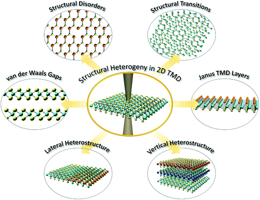 |
| | Fig. 1 Schematic illustrations of the structural heterogeneity in 2D TMD layers. | |
2. Visualization of structural disorders in 2D TMD layers
The unique two-dimensional layered structures of TMD layers have been extensively manifested throughout the literature, where TEM serves as a ubiquitous technique for the direct visualization of the distinctive atomic arrangements, where the structural/chemical disorders may endow/affect the performances of the 2D layers.19,20 The visual observation and verification of the presence of inherent and introduced defects (e.g., vacancies, dislocations, grain boundary defects, dopants, as well as van der Waals gaps) provide valuable information for interpreting the atomic configurations of 2D TMD layers.31,32
2.1 0D defects: vacancies and dopants
The most prevalent type of atomic imperfection is the naturally occurring point defects (i.e., 0D at lattice point). In the case of 2D TMDs (e.g., MX2 with M = Mo, W, and X = S, Se), the point defects routinely take the form of intrinsic vacancies where the transition metal (M), chalcogen (X), or MXn clusters are absent in the lattice, or interchanges between M and X atoms. The most predominantly observed vacancies are the loss of chalcogenide atom(s) which have been consistently observed via TEM. In the representative case of monolayer MoS2 (Fig. 2(a)),33 S atomic losses occur most frequently due to insignificant energetic penalty (e.g., VS, VS2), whereas Mo points defects are often accompanied by the simultaneous absence of neighboring S atoms (e.g., VMoS3, VMoS6), while that of interchanged Mo and S sites have also been observed (e.g., MoS2, S2Mo). It is worth noting that in addition to the inherently occurring vacancies, such atomic imperfections can also be artificially created with designated patterns towards tailoring the TMD layer properties and performances. This defect engineering approach has been demonstrated with irradiation via a focused electron beam (FIB). As shown in Fig. 2(b),34 patterned array of nanopores can be generated via AC-STEM for producing an antidot lattice in monolayer MoS2. Apart from intrinsic vacancy-type defects, the introduction of substituting or adsorbed dopant atoms has been observed. For instance, metallic dopants (e.g., Re) have been evidenced in MoS2 monolayers via ADF-STEM for improving local chemical affinity (Fig. 2(c)).35 We note that foreign adatoms are less explored in monolayer MoS2, since the majority of adatoms have been frequently observed to be Mo and S across multiple sites on the crystal surface (Fig. 2(d))33 owing to their highly favorable adsorption energies.
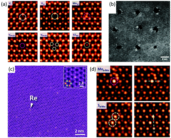 |
| | Fig. 2 (a) STEM-ADF imaging of various typically-observed vacancies (and vacancy complexes) from 2D monolayer MoS2. Reprinted with permission from ref. 33 Copyright 2013 American Chemical Society. (b) STEM-ADF image of patterned 1 nm nanopore arrays upon 30 s duration of drilling. Reproduced with permission from ref. 34 Copyright 2017 Royal Society of Chemistry. (c) Large-area STEM-ADF image of Re-doped monolayer MoS2. The inset demonstrates a dopant Re substituted Mo-site (centered) as revealed by the bright contrast. Reproduced with permission from ref. 35 Copyright 2014 Wiley-VCH Verlag GmbH & Co. KGaA, Weinheim. (d) Adatoms (Mo and S) on single-layer MoS2 as identified via low-pass filtered STEM-ADF (left-side column), and deconvolved images (right-side column). Top-row: Mo adsorbed on top of Mo-site; and bottom-row: single S atoms adsorbed on Mo-sites. Reprinted with permission from ref. 33 Copyright 2013 American Chemical Society. | |
2.2 1D defects: dislocations and inclusion of 1D channels
Another commonly identified defect that occurs in one dimension (1D) is dislocation, especially line defects where the pristine lattice arrangements differ from original periodical patterns. Among the line dislocations of monolayer MoS2, aggregated sulfur (1S) line vacancies have been extensively observed, whose frequent occurrence has been ascribed to the low migration barrier in terms of atomic diffusion.36 Single or multiple lines of S vacancies of various lengths have been experimentally observed along the zig-zag direction (as opposed to the armchair direction) via TEM (Fig. 3(a and b)).37 It has been demonstrated that the MoS2 band structure exhibits a semiconductor-to-metallic transition as such line vacancies are lengthened, manifesting mixed transport phenomena stemming from the metallic-conducting behaviors of these vacancy clusters.38 Specifically, two types of S line vacancy defects have been demonstrated to contribute to establishing the metallic channels as shown by Wang et al. where the line defect widening yields metallic paths (Fig. 3(c)).39
 |
| | Fig. 3 (a) AC-TEM image of line vacancies from single-layer MoS2. (b) High magnification AC-TEM image of an isolated 1S line vacancy, reproduced with permission from ref. 37 Copyright 2018 The Royal Society of Chemistry. (c) AC-TEM image of two adjoining parallel S vacancy lines with different S reconstructions. Scale bar: 0.5 nm. Reproduced with permission from ref. 39 Copyright 2016 American Chemical Society. | |
The transition to lower dimensionality in 2D materials paves a viable avenue towards unleashing further potentials of TMDs where novel chemical/physical properties await discoveries.4 1D defects/interfaces in TMDs harbor distinct phenomena while the 1D/2D interplay can lead to unique properties including lateral confinement effects and electronic transition mediation, as well as dislocation formation suppression.4,40 Therefore, precision nano-sculpting within 2D TMD layers (i.e., lateral dimensional architecting) has attracted growing research investigations for accessing ultimate length scales. Han et al.41 have explored a dislocation-catalyzed approach for the construction of dangling bond free and sub-nanometer MoS2 1D channels coherently embedded within a 2D WSe2 monolayer matrix (ADF-STEM image as shown in Fig. 4(a)). Coherent connection between the 1D MoS2 channel and the 2D WSe2 host layer is distinctively visible at the epitaxial heterointerface. Additionally, a 5|7 dislocation is consistently present at the 1D channel terminal, as shown in the enlarged image in Fig. 4(a). The realization of such clear observation via STEM is attributed to the high contrast between the WSe2 substrate layer and the MoS2 channels due to the difference in W and Mo atomic numbers. Moreover, lateral 1D MoS2 superlattices in 2D WSe2 have been constructed stemming from a periodic dislocation chain. As shown in Fig. 4(b), 1 nm nanowire arrays are grown to the left of the 1D channel, with sub-nm spacing arising from the dislocation sites. Smaller intrusions are also observed at the other side of the 1D channel (right side), which are ascribed to the collective dislocation interactions where the wandering/desolate dislocations are driven to the lower energy side (i.e., the left), leaving the ends of the small intrusions dislocation-free. A further type of 1D channel within 2D layers involves the formation of uni-directional void aggregation. Through in situ TEM, Chen et al. have investigated ultra-long 1D channels in 2D MoS2 monolayers that are composed of sulfur atomic vacancies.42Fig. 4(c) reveals atomically uniform ultra-long linearly aggregated vacancies exhibiting a periodic lattice structure along the zig-zag direction. Notably, the terminus of the zig-zag MoS2 void edges has an MoS wire attached to them due to local S depletion at the edge, as shown in Fig. 4(d).
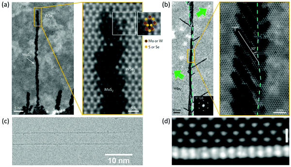 |
| | Fig. 4 (a) ADF-STEM images of sub-nm 1D MoS2 channels embedded in a 2D WSe2 monolayer matrix. The white rectangle area indicates the 5|7 dislocation at the end-of-1D-channel, with the atomic schematics labeled. (b) ADF-STEM images of a superlattice grown from the periodically-appearing dislocations along the WSe2 grain boundary (GB). The blue dashed lines mark the location of the original GB, while the green arrows indicate the dislocation migration directions. The T-shaped marker indicates a class of identical dislocation. Reproduced with permission from ref. 41 Copyright 2017 Macmillan Publishers Limited, part of Springer Nature. (c) Phase-contrast AC-TEM image of MoS2 at 800 °C, revealing ultra-long line defects. (d) ADF-STEM image of the MoS wire as adhered to the MoS2 zig-zag edge. Scale bar: 0.5 nm. (c and d) Reproduced with permission from ref. 42 Copyright 2018 American Chemical Society. | |
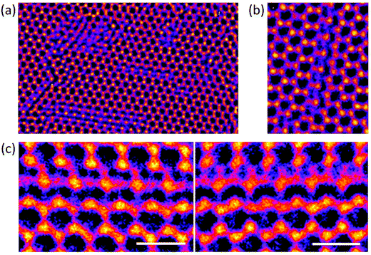
2.3 Grain boundaries
In addition to line vacancies, grain boundaries (GBs) are another frequently encountered defects, where grains with mismatched crystal orientations adjoin at the dislocation cores.43 Grain boundaries have been demonstrated to exhibit unique electrical, optical, and catalytic properties across a wide range of 2D TMDs.44–48 These GB dislocation cores across the grain boundaries are mostly observed to take the form of 5- and 7-fold (5|7) rings (Fig. 5(a)),43 with 4|6 and 6|8 rings also being identified. Additionally, TEM also serves as a powerful tool in assessing the evolution of grain boundary defects, tracking the migration of GBs. Azizi et al. have identified the GB dislocation motion in WS2, where they demonstrated dislocation glide along a specific Burgers vector.49 Initial observation revealed tilt GB with a 12° misorientation angle in the monolayer of WS2 (Fig. 5(b),49 showing a 6|8 edge dislocation). Continuous atomic-level dynamics yields migration of the 6|8 edge dislocation along the (1,0) Burgers vector on the glide plane (Fig. 5(c)).49 The manipulation of GBs provides a useful pathway towards defect engineering, where GBs can have a significant influence on the local band structure of 2D TMDs (e.g., introducing mid-gap states33) due to their different TM/D stoichiometry and coordination.37
 |
| | Fig. 5 (a) STEM-ADF images of common grain boundary dislocations in monolayer MoS2 showing a 5|7-fold ring (top) and its variant (bottom) with S-substitution at the Mo-site. Purple and yellow circles indicate Mo and S2 columns, respectively. Reprinted with permission from ref. 43 Copyright 2013 Macmillan Publishers Limited. (b) (i) The ADF-STEM image of a tilt grain boundary in monolayer WS2 with the corresponding fast Fourier transform patterns shown in the inset (scale bar: 2 nm). The dashed line indicates the misorientation angle of 12° between different grains (scale bar: 0.5 nm). (ii) The ADF-STEM image (top-row) of a 6|8 dislocation core in the 12° grain boundary, and (bottom-row) the positions of W and S in the 6|8 dislocation (scale bar: 0.5 nm). (c) Dislocation migration in the 12° grain boundary of WS2 along the (1,0) Burgers vector on the glide plane (marked by the white dashed lines) from (i) to (ii) precisely 5 seconds apart. Scale bar: 0.6 nm. Reprinted with permission from ref. 49 Copyright 2014 Macmillan Publishers Limited. | |
2.4 van der Waals gaps
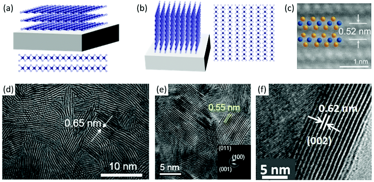
As a distinct atomic feature of 2D TMDs, van der Waals (vdW) gaps between the atomic layers are a bedrock for the unique electronic/optoelectronic properties of the corresponding 2D TMD materials and devices.50–53 Extensive efforts have been devoted to the direct visualization of the vdW gaps and stacking configurations among a wide spectrum of 2D TMD materials including 2D MoS2, WS2, PtSe2, PtTe2 layers and their heterostructures/heterointerfaces (schematic illustrations of horizontally and vertically aligned 2D layers are shown in Fig. 6(a and b) respectively54).7,8,55 The atomic-scale continuous high-homogeneity horizontal stacking of 2D PtTe2 layers is shown in Fig. 6(c)56 as revealed via HAADF-STEM, exhibiting the distinct crystalline structure with well-resolved vdW gaps (∼0.52 nm). In addition, vertically-aligned (VA) 2D MoS2 layers have also been demonstrated as identified via HR-TEM (Fig. 6(d)),57 showing uniformly-spaced vdW gaps. Moreover, integral VA 2D PtSe2 layers have been observed via HR-TEM (Fig. 6(e)),54 exhibiting well-defined vdW gaps of ∼0.55 nm. Further types of VA 2D TMDs have been revealed via HR-TEM including a few-layer single-crystalline 2D WS2 sheet as shown in Fig. 6(f), revealing the well-resolved stacking of WS2 (002) layers exhibiting an interlayer spacing of ∼0.62 nm.58
 |
| | Fig. 6 (a) Schematic illustrations of horizontally-aligned 2D TMD layers as grown on the substrate, with atomic layer arrangements shown at the lower half.54 (b) Schematic illustrations of vertically-aligned 2D TMD layers as grown on the substrate, with atomic layer arrangements shown at the right side.54 Reproduced with permission from ref. 54 Copyright 2020 American Chemical Society. (c) Cross-sectional HAADF-STEM image of 2D PtTe2 layers exhibiting an interlayer spacing of ∼0.52 nm with a layer-stacking sequence of (1T) Te–Pt–Te atomic chains (blue and yellow dots indicate Pt and Te atoms, respectively).56 Reproduced with permission from ref. 56 Copyright 2020 American Chemical Society. (d) HR-TEM image of the as-grown vertically-aligned 2D MoS2 layers, showing surface-exposed edges with evenly-spaced (∼0.65 nm) vdW gaps.57 Reproduced with permission from ref. 57 Copyright 2020 American Chemical Society. (e) HR-TEM image of vertically-aligned 2D PtSe2 layers. The inset shows the corresponding SAED pattern indexing the PtSe2 crystalline planes.54 Reproduced with permission from ref. 54 Copyright 2020 American Chemical Society. (f) HR-TEM image of 2D WS2 (002) layers with an interlayer spacing of ∼0.62 nm.58 | |
3. Visualization of heterointerfaces in 2D TMD layers
3.1 2D/2D vertical heterointerfaces
Apart from homogenous 2D TMD layers, the heterointerfaces at the adjacent stacked layers of 2D heterostructures are also of intense interest due to their potential as a new type of hybrid material exhibiting superior opto-electrical properties with elevated strain limit.59–61 For instance, Choudhary et al. have demonstrated a few-layer vertically-stacked MoS2/WS2 heterostructure film at centimeter-scale with a clean heterointerface as revealed via HR-TEM (Fig. 7(a)).62 Moreover, ADF-STEM characterization of the same MoS2/WS2 heterointerface yields a brighter image contrast for WS2 compared to that of MoS2 layers (Fig. 7(b), left), while EDS-STEM elemental mapping (Fig. 7(b), right) reveals a highly localized spatial distribution of Mo and W atoms across the MoS2/WS2 heterointerface.62 Furthermore, Li et al. have demonstrated VSe2/WSe2 vertical heterostructures with near-ideal atomically-clean vdW heterointerfaces (Fig. 7(c)).16 In addition, more complex 2D heterostructures have been realized via molecular beam epitaxy (MBE) as an effective synthetic route.63 For instance, Kang et al. reported the realization of wafer-scale vertical stacking of 2D TMD heterostructures (cross-sectional STEM image of a MoSe2/MoS2/WS2 film shown in Fig. 7(d)),64 demonstrating a viable strategy of programmed vacuum stack (PVS) assisted layer-by-layer assembly for large-scale production while retaining clean interfaces and pure interlayers, despite lattice mismatch or layer rotation.
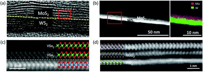 |
| | Fig. 7 (a) HR-TEM image of a vertically-stacked MoS2/WS2 heterostructure, showing a distinct MoS2/WS2 heterointerface.62 (b) Cross-sectional ADF-STEM image of a vertically-stacked few-layer MoS2/WS2 heterostructure (left-side), and the corresponding EDS-STEM elemental mapping (right-side).62 (c) HR-STEM image of the VSe2/WSe2 vdW heterointerface (the white dashed line indicating the heterojunction interface, with the corresponding atomic models for VSe2 and WSe2 shown at the upper and lower half, respectively, across the interface).16 Reproduced with permission from ref. 16 Copyright 2020 Springer Nature Limited. (d) Cross-sectional STEM image of a MoSe2/MoS2/WS2 film. Reproduced with permission from ref. 64 Copyright 2017 Macmillan Publishers Limited, part of Springer Nature. | |
3.2 2D/2D in-plane heterointerfaces
In addition to the vertically-assembled 2D TMD layers, in-plane heterointerface engineering has also received considerable attention for reducing lattice mismatch.65 Many investigations have explored the feasibility of direction in-surface construction/patterning of heterointerfaces within 2D TMD layers, including layer restructuring.66,67
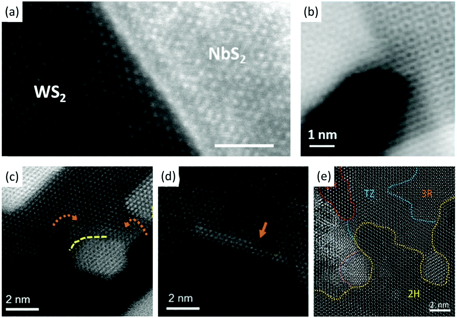
The realization of lateral heterostructures in 2D TMDs has enabled unique electronic properties in heterojunctions stemming from nanofabricated stacking configurations.68–70 For instance, Zhang et al. have demonstrated a monolayer NbS2–WS2 lateral heterostructure via edge-epitaxial growth.71 They have shown via TEM the distinct chemical modulation exhibiting well-resolved interfaces (Fig. 8(a)). Furthermore, Tai et al. have developed an in situ STEM/TEM-based approach to construct 2D few-layer MoS2 lateral heterojunctions with various 2D architectures (Fig. 8(b–e)).72 With electron beam MoS2 layer-thinning, a heterointerface between monolayer and few-layer 2D MoS2 is demonstrated via dark-field STEM (Fig. 8(b)) as manifested by different Moiré patterns. In addition, based on electron beam etching, a folding behavior was observed, evolving from particles to hexagonal plates (Fig. 8(c)). Additionally, scrolling of MoS2 layers was also identified apart from folding (shown in Fig. 8(d)). The formation of nanoscrolls was attributed to the surface energy compensation of the dangling-bond-rich edges. Moreover, quantification of layer number/thickness can be realized via the normalization of the image intensity of a single Mo/S atom within the 1H phase monolayer since the contrast intensity has linear proportionality with the atomic mass.73 As a distinct feature of the vdW interactions, manifold categories of MoS2 polytypes provide further opportunities in constructing additional classes of heterostructures. Such an approach may lead to extended handles of the physical properties since the varied stacking orders exhibit different interlayer distances. Therefore, lateral heterojunctions composed of distinct polytypes integrated in-plane have been demonstrated as shown in Fig. 8(e) with various types of stacking sequences identified (i.e., 1H, 2H, 3R, 3R′, and transitional zone). The ABB stacking of 3R′ shows a strong mass signal with a higher contrast due to the tri-fold layer structure, whereas the transitional zone (TZ) exhibits in-plane mis-alignment.
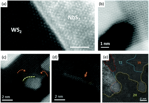 |
| | Fig. 8 (a) HAADF-STEM image of an NbS2–WS2 lateral heterostructure, revealing a clean NbS2–WS2 in-plane heterointerface (scale bar: 2 nm).71 Reprinted with permission from ref. 71 Copyright 2018 Wiley-VCH Verlag GmbH & Co. KGaA, Weinheim. (b) HR-dark-field-STEM image of a monolayer/few-layer 2D MoS2 heterointerface as distinguished via different Moiré patterns.72 (c) HR-STEM image of the folding process of 2D MoS2 layer. The yellow dashed line indicates the growth of nanoflakes, while the orange arrows mark the folding direction.72 (d) HR-STEM image of the scrolling process of the 2D MoS2 layer (with the orange arrow marking the nanoscroll).72 (e) ADF-STEM image of the MoS2 lateral heterointerface with the dashed lines indicating the regime boundaries along different in-plane polytypes.72 Reprinted with permission from ref. 72 Copyright 2019 Wiley-VCH Verlag GmbH & Co. KGaA, Weinheim. | |
3.3 Strained 2D/2D interfaces
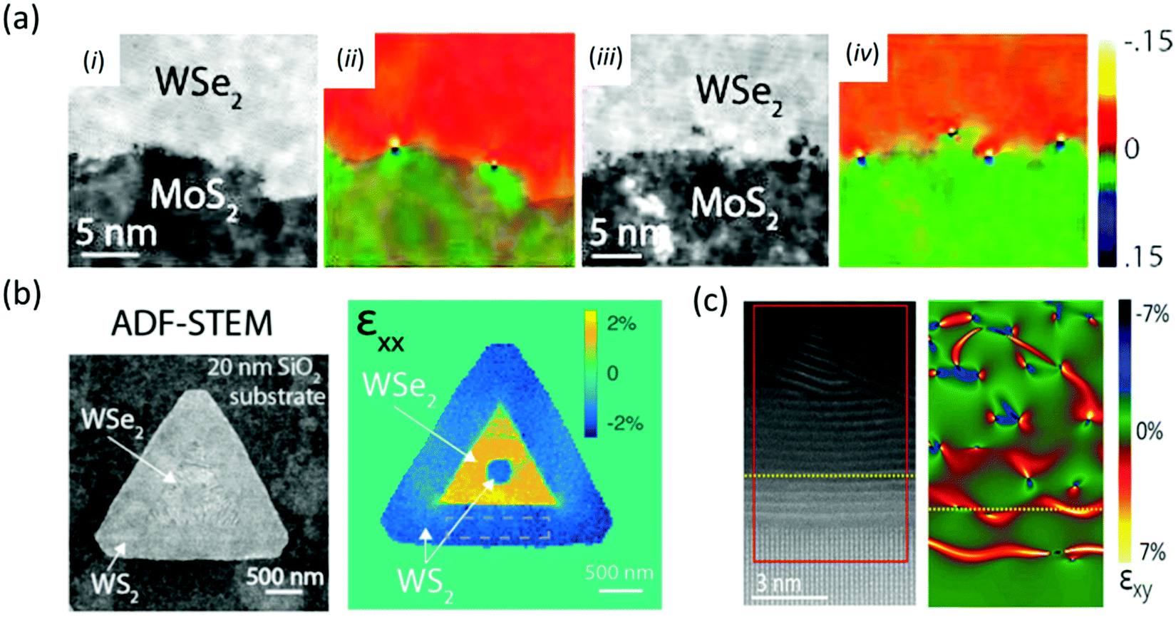
2D lateral heterostructures, due to their tunable band offset and highly sensitive in-plane heterointerfaces, are a promising class of 2D TMD constructs with unique properties. The obstacle of lattice mismatch presents a hindrance towards realizing the full potential of their desired performances. In this regard, strain modulation proves to be a viable approach in achieving coherent superlattices laterally integrating different TMD monolayers. Han et al. have revealed the presence of strains at the 2D MoS2/WSe2 lateral interface via ADF-STEM accompanied by the corresponding εxx strain maps.41 The uniaxial strain maps (Fig. 9(a)) identify a distinct contrast difference across the 2D MoS2/WSe2 interface, indicating a lattice mismatch at the abrupt junctions as well as interfacial misfit dislocations. Moreover, high precision strain-mapping towards the 2D WS2/WSe2 lateral heterostructure similarly unveiled the presence of an x-direction uniaxial strain at the WS2/WSe2 2D lateral layer boundaries.74 The ADF-STEM image with its corresponding εxx strain map (Fig. 9(b)) at the WS2/WSe2 2D lateral heterojunction interface revealed a strained 2D heterointerface with minor localized deviations. Such well-mapped interfacial strain contrasts are predominantly ascribed to the WS2/WSe2 lattice mismatch, in addition to misfit dislocations to a lesser extent. Furthermore, Choudhary et al. have revealed the local strain in 2D MoS2 layers in a horizontal-to-vertical transition via TEM geometric phase analysis (GPA).75 The differentiated (false) colors, as shown in Fig. 9(c), indicate the considerable local (shear) strain within horizontal-to-vertical transition 2D MoS2 layers, which are identified via ADF-STEM (i.e., the upper half of the red rectangle box).
 |
| | Fig. 9 (a) ADF-STEM images ((i) and (iii)) of the 2D MoS2/WSe2 lateral layer and the corresponding εxx strain maps ((ii) and (iv) respectively). Reproduced with permission from ref. 41 Copyright 2017 Macmillan Publishers Limited, part of Springer Nature. (b) ADF-STEM image of the 2D WS2/WSe2 lateral heterojunction via 4D data from an electron microscope pixel array detector, and the associated uniaxial strain (εxx) map. Reprinted with permission from ref. 74 Copyright 2018 American Chemical Society. (c) Left: The ADF-STEM image of 2D MoS2 layers in a horizontal-to-vertical transition (the yellow dashed line represents the 2D MoS2/WS2 interface); right: TEM geometric phase analysis (GPA) strain map corresponding to the red box in the left image (yellow dashed line denotes the 2D MoS2/WS2 interface).75 Reproduced with permission from ref. 75 Copyright 2018 Wiley-VCH Verlag GmbH & Co. KGaA, Weinheim. | |
3.4 Janus monolayer 2D TMDs
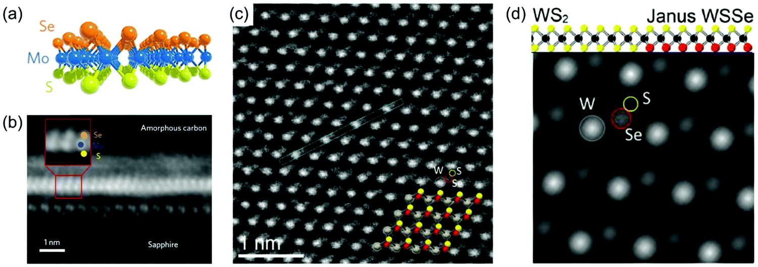
Based on the understanding of the fundamental mechanisms of interaction between atoms and the electron beam, TEM can be used as a valuable tool towards visualizing the atomic-scale characteristics of 2D TMDs including void formation in the MoS2 monolayer,42 defects, and dopants in 2D TMDs,37,76 as well as distinguishing asymmetric Janus structures of the MoSSe monolayer.77,78 In an effort to extend the degree of freedom in TMD monolayers, which show an intrinsic in-plane inversion asymmetry, Lu et al. reported a synthetic strategy to grow the Janus monolayer of TMDs, breaking the out-of-plane structural symmetry.77 In particular, they replaced the top-layer S with Se atoms based on a monolayer MoS2.77 Using an annular dark-field scanning TEM (ADF-STEM), they observed a cross-section of the asymmetric Janus structure of the MoSSe monolayer, which clearly distinguishes bottom S and top Se atoms as shown in Fig. 10(a and b),77 as the image contrast is proportional to the square of the atomic number. A further example of the Janus structure of the MoSSe monolayer produced via controlled sulfurization of monolayer MoSe2 (i.e., top Se substituted by S) was also identified via HR-TEM.78 Moreover, as shown in Fig. 10(c and d), Lin et al. observed a WSSe Janus monolayer as prepared by low energy implementation using tilted high angle annular dark field Z-contrast scanning transmission electron microscopy (HAADF-Z-STEM) to visualize the Janus structure where top S and bottom Se are distinguished by their image intensities.79 Additionally, atomic resolution low-voltage scanning TEM (STEM) imaging with atom-by-atom analysis can also be employed to examine the atomic alloy behavior of several molybdenum and tungsten ditelluride monolayers alloyed with sulfur or selenium (MX2xTe2(1−x), M = Mo, W, and X = S, Se) in both 2H and 1T′ phases and with different alloy concentrations as Z-contrast STEM imaging is directly related to the atomic number of the imaged species.80
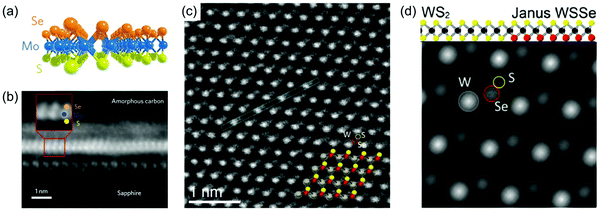 |
| | Fig. 10 (a) Molecular model of synthesized Janus MoSSe monolayer.77 (b) ADF-STEM image of a cross-section of the Janus MoSSe monolayer of (a).77 Reproduced with permission from ref. 77 Copyright 2017 Macmillan Publishers Limited, part of Springer Nature. (c) Tilted HAADF-Z-STEM images of ML Janus WSSe tilted at x = +15° along with the overlaid ball-and-stick model showing W atoms (gray), Se atoms (red), and S atoms (yellow).79 (d) Molecular model of Janus WSSe monolayer (top) and the corresponding simulated STEM image for Janus WSSe tilted at x = +15°, which confirms the relative intensity ratio measured experimentally on (c).79 Reproduced with permission from ref. 79 Copyright 2020 American Chemical Society. | |
4. Atomic-scale in situ visualization of structural and chemical transitions in 2D TMD layers
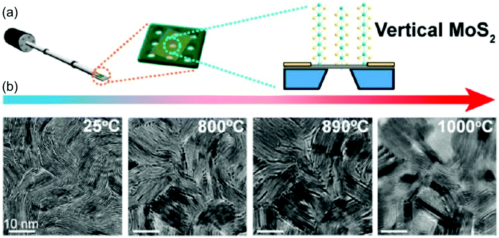
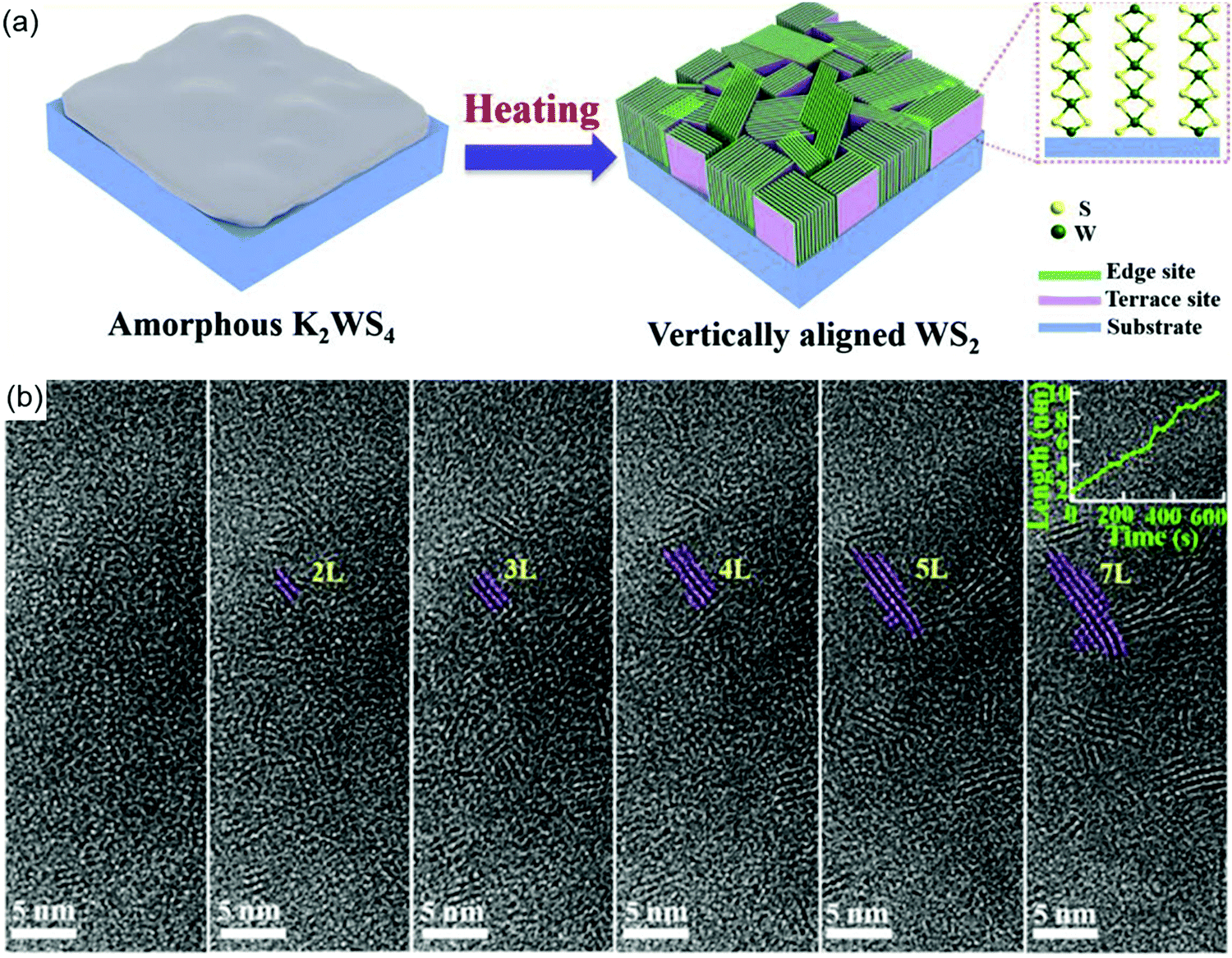
In situ TEM characterization of 2D TMD layers under an external stimulus (e.g., temperature variations) has recently emerged since the high temporal resolution and high detector frame rate requirement (e.g., 100 frames per second or faster) can be achieved via minimizing the electron dose per frame.81 To target maximized temporal resolutions, the adoption of direct detectors in integrating modes is preferred while minimizing the electron beam dose in order to visualize the dynamic evolutions during the crystal transition of 2D TMD layered materials.81 As a powerful advanced characterization technique, in situ TEM endows the possibility of direct visualization of the atomic-scale 2D layer structural dynamics on small-length scales.32,82 For instance, recent studies on horizontal MoS2 or their monolayer counterparts via in situ TEM have investigated the kinetics of thermolysis-driven 2D MoS2 layer growth via in situ heating.19,83 While previous studies focused on horizontally-aligned 2D MoS2 layers, Wang et al. demonstrated a real-time in situ TEM observation (bright-field HR-TEM and dark-field STEM) of vertically-aligned 2D MoS2 layers under controlled heating from room temperature up to 1000 °C, as shown in Fig. 11(a).82 Direct in situ heating and monitoring of vertically-aligned 2D MoS2 layers allowed visualization of comprehensive in situ heating TEM study on transferred, vertically-aligned MoS2 layers up to 1000 °C, as shown in Fig. 11(b).82 At ∼875 °C, the formation and growth of voids between the domains of vertically-aligned 2D layers in distinct orientation were observed while Mo nanoparticles start to form during the subsequent decomposition of 2D MoS2 layers at ∼950 °C (i.e., a significantly lower temperature compared to the melting temperature of bulk MoS2).82 Additionally, pronounced migrations of 2D MoS2 layers at the junctions formed by multiple grains of large bending angles were observed, which are believed to be driven by the release of the accumulating strain for reducing total interfacial energy.82 Moreover, it was identified that surface-exposed defective 2D layer edge sites are the triggering points for the thermal decomposition of S atoms and the subsequent decomposition of 2D MoS2 layers.82 Furthermore, Zhang et al. achieved the controlled growth of vertically-aligned 2D WS2 with high-temperature stability from in situ heating TEM investigations, as shown in Fig. 12.84 Amorphous precursor K2WS4 in TEM was synthesized into vertically-aligned WS2, as shown in Fig. 12(a).84Fig. 12(b) shows the HR-TEM images clarifying the layer-by-layer growth dynamics from the amorphous state of the precursor to the vertically-stacked WS2 layers during continuous heating at 150 °C.84 The HR-TEM images demonstrated the layer-by-layer growth dynamics of vertically-aligned 2D WS2 structures at 150 °C.84 The evolution of the vertically-aligned 2D WS2 was further investigated using in situ TEM heating experiments at different heating temperatures to understand the growth mechanism and the thermolysis of a solid precursor (NH4)2WS4.84 Leiter et al. investigated the dynamics of the formation of electron-beam induced defects in monolayer WSe2via in situ spherical and chromatic aberration-corrected low-voltage HR-TEM, which lays the foundation of the basic understanding of defect dynamics in monolayer WSe2.85 Additionally, Liu et al. identified the material formation of sub-1 nm ribbon as a Mo5S4 crystal derived from layered MoS2, serving as a precursor using dynamic in situ HR-TEM characterization.86 In addition, Chen et al. revealed the process of producing atomically flat Mo terminated zig-zag edges in nanoribbons using in situ aberration-corrected TEM (AC-TEM) by way of heating monolayer MoS2 to 800 °C in vacuum, thus enabling the direct imaging of atomic structure in 2D materials while resolving clear edge terminations.87
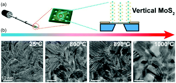 |
| | Fig. 11 (a) MoS2 integration to an in situ TEM holder (left) of CVD-grown vertically-aligned 2D MoS2 layers (right).82 (b) TEM snapshots of vertically-aligned 2D MoS2 layers during in situ heating from 800 °C up to 1000 °C, revealing various structural evolutions, including void formation and growth.82 Reprinted with permission from ref. 82 Copyright 2019 American Chemical Society. | |
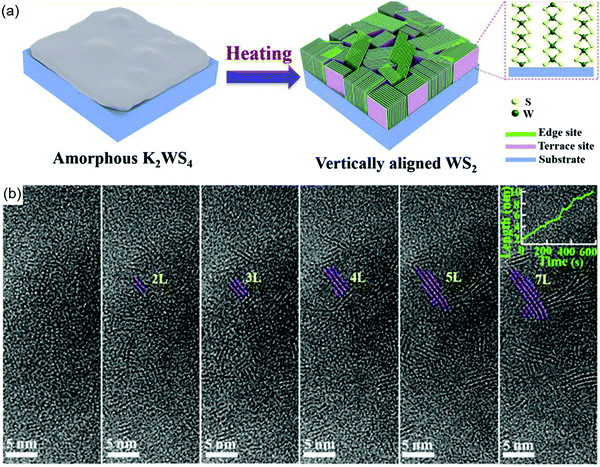 |
| | Fig. 12 (a) Schematic diagram of the transformation from a solid amorphous precursor to vertically aligned WS2 by in situ TEM heating.84 (b) Layer-by-layer growth dynamics of the vertically aligned WS2 structure at 150 °C. Time-resolved in situ TEM image series at 0 s, 88 s, 158 s, 279 s, 535 s, and 738 s, respectively, where colored sketches illustrate the WS2 layers. Note: the inset graph on the right shows the projected length of 2L slabs at different heating times. Reprinted with permission from ref. 84 Copyright 2019 Elsevier Ltd. | |
Moreover, scanning transmission electron microscopy (STEM) has also been extensively utilized in 2D TMD characterizations due to its high spatial and temporal resolution at lower atomic numbers compared to TEM. The contrast in STEM images is intrinsically related to the atomic weight (called Z-contrast), which allows for tracking specific elements in the lattice.88 Kumar et al. directly visualized ordered MoS2 nanocrystal formation in atomically thin layers upon heating using in situ ADF-STEM towards observing its strong dependence on the heating rate and temperature for the resulting structures and phases.89 Additionally, Sang et al. performed in situ heating experiments using AC-STEM to track the edge evolution and transformation in a Mo1−xWxSe2 (x![[thin space (1/6-em)]](https://www.rsc.org/images/entities/char_2009.gif) = 0.05) monolayer. They demonstrated that by varying the local chemical environment, the formation of nanopores could be triggered, with the nanopores terminated by different edge reconstructions during in situ heating and electron beam irradiation, while the formed edge structures exhibit metallic and/or magnetic properties.90
= 0.05) monolayer. They demonstrated that by varying the local chemical environment, the formation of nanopores could be triggered, with the nanopores terminated by different edge reconstructions during in situ heating and electron beam irradiation, while the formed edge structures exhibit metallic and/or magnetic properties.90
5. Conclusions and outlooks
As a “re-discovered” promising class of high-performing materials with various intriguing properties and superior application potentials, 2D TMD layers and their heterostructures continue to be at the frontier of materials sciences and nanotechnologies, both in terms of fundamental atomic-scale phenomena investigations and device-oriented product development. In the present review, recent studies on the TEM investigations of 2D TMD mono- and hetero-layer atomic defects, as well as 2D TMD-based heterostructures with their heterointerface features are overviewed. Technological progress in advanced modes of TEM (e.g., AC-TEM and ADF-STEM) has yielded valued direct characterization and visualization techniques for realizing atomic-scale identification and manipulation of defects and heterointerfaces. The considerable advancement in this field is a testament to the thriving potentials of exploring the possibilities of the emerging defect and heterointerface configurations and their impact on materials and device properties. For instance, it is anticipated that advanced TEM techniques will play an essential role in the fabrication and characterization of recently discovered 2D bilayer superlattices with specific angles (also known as super angles).91–93 The vertical stacks of two 2D layers forming bilayer with a twist angle results in the formation of a superlattice, exhibiting extraordinary electrical and optical properties. The superlattice-induced special features (e.g., superconductivity, Moiré excitons, and interlayer decoupling) have been attributed to the interlayer electronic coupling enhanced by surface-exposed electronic states as well as quantum confinement.92,94–96 In these twisted bilayers, the misalignment angle is the main factor determining the electronic structure so that the direct observation of structural heterogeny using TEM-based analytic tools, e.g., fast Fourier transform, can provide valuable information.92 Moreover, TEM unveils an additional avenue for precision atomic-scale defect and interface engineering in 2D TMD layers and heterostructures, which serves as the basis for targeted design towards uncovering novel material properties and device performances. The atomic-scale characterization of 2D TMD layers and their heterointerfaces is expected to continue to act as an insightful approach towards understanding the defect/interfacial structures and the associated influence on material/device properties and performances. In particular, the in-depth investigations on defect manipulation as well as lattice evolutionary behaviors and underlying mechanisms are both desirable and potentially challenging, especially via in situ TEM techniques. Additionally, the irreversible structure degradation due to extended electron team irradiation exposure could hamper chemical component analysis efforts, thus further reduction in image acquisition time is favorable, potentially via double energy-filtered STEM technique. Overall, with collaborative studies for future 2D materials design especially when combined with computational techniques, it is therefore expected that revealing the meticulous modulation of the location, composition, and extent of the defects and (hetero)interfaces using TEM-based tools (e.g., high-resolution STEM and strain map analysis) would receive growing attention in various application-oriented fields towards electronic, optoelectronic, sensing, catalytic, and atomic-scale filtering devices.
Author contributions
Writing – original draft: H. L., C. Y., and T.-J. K.; writing – review & editing: H. L., C. Y., T.-J. K., and J. H. K.; supervision: H. L. and Y. J.
Conflicts of interest
The authors declare no competing interests.
References
- Q. H. Wang, K. Kalantar-Zadeh, A. Kis, J. N. Coleman and M. S. Strano, Nat. Nanotechnol., 2012, 7, 699–712 CrossRef CAS PubMed
 .
.
- C. Gong, H. Zhang, W. Wang, L. Colombo, R. M. Wallace and K. Cho, Appl. Phys. Lett., 2013, 103, 053513 CrossRef .
- H. Zhang, M. Chhowalla and Z. Liu, Chem. Soc. Rev., 2018, 47, 3015–3017 RSC .
- T. Chowdhury, E. C. Sadler and T. J. Kempa, Chem. Rev., 2020, 120, 12563–12591 CrossRef CAS PubMed .
- G. R. Bhimanapati, Z. Lin, V. Meunier, Y. Jung, J. Cha, S. Das, D. Xiao, Y. Son, M. S. Strano, V. R. Cooper, L. Liang, S. G. Louie, E. Ringe, W. Zhou, S. S. Kim, R. R. Naik, B. G. Sumpter, H. Terrones, F. Xia, Y. Wang, J. Zhu, D. Akinwande, N. Alem, J. A. Schuller, R. E. Schaak, M. Terrones and J. A. Robinson, ACS Nano, 2015, 9, 11509–11539 CrossRef CAS PubMed .
- T.-J. Ko, H. Li, S. A. Mofid, C. Yoo, E. Okogbue, S. S. Han, M. S. Shawkat, A. Krishnaprasad, M. M. Islam, D. Dev, Y. Shin, K. H. Oh, G.-H. Lee, T. Roy and Y. Jung, iScience, 2020, 23, 101676 CrossRef CAS PubMed .
- M. Wang, H. Li, T.-J. Ko, M. S. Shawkat, E. Okogbue, C. Yoo, S. S. Han, M. A. Islam, K. H. Oh and Y. Jung, J. Mater. Res., 2020, 35, 1350–1368 CrossRef CAS .
- T.-J. Ko, M. Wang, C. Yoo, E. Okogbue, M. A. Islam, H. Li, M. S. Shawkat, S. S. Han, K. H. Oh and Y. Jung, J. Phys. D: Appl. Phys., 2020, 53, 313002 CrossRef CAS .
- J. Ping, Z. Fan, M. Sindoro, Y. Ying and H. Zhang, Adv. Funct. Mater., 2017, 27, 1605817 CrossRef .
- D. Voiry, J. Yang and M. Chhowalla, Adv. Mater., 2016, 28, 6197–6206 CrossRef CAS PubMed .
- J. He, K. Hummer and C. Franchini, Phys. Rev. B: Condens. Matter Mater. Phys., 2014, 89, 075409 CrossRef .
- H. Zhang, ACS Nano, 2015, 9, 9451–9469 CrossRef CAS PubMed .
- S. Wang, H. Sawada, C. S. Allen, A. I. Kirkland and J. H. Warner, Nanoscale, 2017, 9, 13060–13068 RSC .
- K. Elibol, T. Susi, G. Argentero, M. Reza Ahmadpour Monazam, T. J. Pennycook, J. C. Meyer and J. Kotakoski, Chem. Mater., 2018, 30, 1230–1238 CrossRef CAS PubMed .
- M. Chhowalla, H. S. Shin, G. Eda, L.-J. Li, K. P. Loh and H. Zhang, Nat. Chem., 2013, 5, 263 CrossRef PubMed .
- J. Li, X. Yang, Y. Liu, B. Huang, R. Wu, Z. Zhang, B. Zhao, H. Ma, W. Dang, Z. Wei, K. Wang, Z. Lin, X. Yan, M. Sun, B. Li, X. Pan, J. Luo, G. Zhang, Y. Liu, Y. Huang, X. Duan and X. Duan, Nature, 2020, 579, 368–374 CrossRef CAS PubMed .
- X. Duan, C. Wang, A. Pan, R. Yu and X. Duan, Chem. Soc. Rev., 2015, 44, 8859–8876 RSC .
- I. Pallecchi, N. Manca, B. Patil, L. Pellegrino and D. Marré, Nano Futures, 2020, 4, 032008 CrossRef CAS .
- L. Fei, S. Lei, W.-B. Zhang, W. Lu, Z. Lin, C. H. Lam, Y. Chai and Y. Wang, Nat. Commun., 2016, 7, 1–7 Search PubMed .
- P. Gao, L. Wang, Y. Zhang, Y. Huang and K. Liu, ACS Nano, 2015, 9, 11296–11301 CrossRef CAS PubMed .
- W. Choi, N. Choudhary, G. H. Han, J. Park, D. Akinwande and Y. H. Lee, Mater. Today, 2017, 20, 116–130 CrossRef CAS .
- H. Wang, H. Yuan, S. S. Hong, Y. Li and Y. Cui, Chem. Soc. Rev., 2015, 44, 2664–2680 RSC .
- P. Rivera, J. R. Schaibley, A. M. Jones, J. S. Ross, S. Wu, G. Aivazian, P. Klement, K. Seyler, G. Clark, N. J. Ghimire, J. Yan, D. G. Mandrus, W. Yao and X. Xu, Nat. Commun., 2015, 6, 6242 CrossRef CAS PubMed .
- R. Ribeiro-Palau, C. Zhang, K. Watanabe, T. Taniguchi, J. Hone and C. R. Dean, Science, 2018, 361, 690–693 CrossRef CAS .
-
J. Chen and J. H. Warner, in 2D Semiconductor Materials and Devices, ed. D. Chi, K. E. J. Goh and A. T. S. Wee, Elsevier, 2020, pp. 167–197 DOI:10.1016/B978-0-12-816187-6.00006-6 .
- Z. Lin, A. Yin, J. Mao, Y. Xia, N. Kempf, Q. He, Y. Wang, C.-Y. Chen, Y. Zhang, V. Ozolins, Z. Ren, Y. Huang and X. Duan, Sci. Adv., 2016, 2, e1600993 CrossRef PubMed .
- L. Tao, K. Chen, Z. Chen, W. Chen, X. Gui, H. Chen, X. Li and J.-B. Xu, ACS Appl. Mater. Interfaces, 2017, 9, 12073–12081 CrossRef CAS PubMed .
- H. Li, T.-J. Ko, M. Lee, H.-S. Chung, S. S. Han, K. H. Oh, A. Sadmani, H. Kang and Y. Jung, Nano Lett., 2019, 19, 5194–5204 CrossRef CAS PubMed .
-
C. B. Carter and D. B. Williams, Transmission electron microscopy: Diffraction, imaging, and spectrometry, Springer, 2016 Search PubMed .
- Y. Shi, H. Li and L.-J. Li, Chem. Soc. Rev., 2015, 44, 2744–2756 RSC .
- Z. Lin, A. McCreary, N. Briggs, S. Subramanian, K. Zhang, Y. Sun, X. Li, N. J. Borys, H. Yuan and S. K. Fullerton-Shirey, 2D Mater., 2016, 3, 042001 CrossRef .
- C. Luo, C. Wang, X. Wu, J. Zhang and J. Chu, Small, 2017, 13, 1604259 CrossRef PubMed .
- W. Zhou, X. Zou, S. Najmaei, Z. Liu, Y. Shi, J. Kong, J. Lou, P. M. Ajayan, B. I. Yakobson and J.-C. Idrobo, Nano Lett., 2013, 13, 2615–2622 CrossRef CAS PubMed .
- S. Wang, H. Li, H. Sawada, C. S. Allen, A. I. Kirkland, J. C. Grossman and J. H. Warner, Nanoscale, 2017, 9, 6417–6426 RSC .
- Y. C. Lin, D. O. Dumcenco, H. P. Komsa, Y. Niimi, A. V. Krasheninnikov, Y. S. Huang and K. Suenaga, Adv. Mater., 2014, 26, 2857–2861 CrossRef CAS PubMed .
- Y. Han, T. Hu, R. Li, J. Zhou and J. Dong, Phys. Chem. Chem. Phys., 2015, 17, 3813–3819 RSC .
- S. Wang, A. Robertson and J. H. Warner, Chem. Soc. Rev., 2018, 47, 6764–6794 RSC .
- H. Liu, L. Jiao, F. Yang, Y. Cai, X. Wu, W. Ho, C. Gao, J. Jia, N. Wang, H. Fan, W. Yao and M. Xie, Phys. Rev. Lett., 2014, 113, 066105 CrossRef CAS PubMed .
- S. Wang, G.-D. Lee, S. Lee, E. Yoon and J. H. Warner, ACS Nano, 2016, 10, 5419–5430 CrossRef CAS PubMed .
- J. Deng, Y. Su, D. Liu, P. Yang, B. Liu and C. Liu, Chem. Rev., 2019, 119, 9221–9259 CrossRef CAS PubMed .
- Y. Han, M.-Y. Li, G.-S. Jung, M. A. Marsalis, Z. Qin, M. J. Buehler, L.-J. Li and D. A. Muller, Nat. Mater., 2018, 17, 129–133 CrossRef CAS PubMed .
- Q. Chen, H. Li, S. Zhou, W. Xu, J. Chen, H. Sawada, C. S. Allen, A. I. Kirkland, J. C. Grossman and J. H. Warner, ACS Nano, 2018, 12, 7721–7730 CrossRef CAS PubMed .
- S. Najmaei, Z. Liu, W. Zhou, X. Zou, G. Shi, S. Lei, B. I. Yakobson, J.-C. Idrobo, P. M. Ajayan and J. Lou, Nat. Mater., 2013, 12, 754 CrossRef CAS PubMed .
- A. M. Van Der Zande, P. Y. Huang, D. A. Chenet, T. C. Berkelbach, Y. You, G.-H. Lee, T. F. Heinz, D. R. Reichman, D. A. Muller and J. C. Hone, Nat. Mater., 2013, 12, 554 CrossRef CAS PubMed .
- T. Kosmala, H. Coy Diaz, H. P. Komsa, Y. Ma, A. V. Krasheninnikov, M. Batzill and S. Agnoli, Adv. Energy Mater., 2018, 8, 1800031 CrossRef .
- Y. Gong, J. Lin, X. Wang, G. Shi, S. Lei, Z. Lin, X. Zou, G. Ye, R. Vajtai, B. I. Yakobson, H. Terrones, M. Terrones, B. K. Tay, J. Lou, S. T. Pantelides, Z. Liu, W. Zhou and P. M. Ajayan, Nat. Mater., 2014, 13, 1135–1142 CrossRef CAS PubMed .
- C. Huang, S. Wu, A. M. Sanchez, J. J. Peters, R. Beanland, J. S. Ross, P. Rivera, W. Yao, D. H. Cobden and X. Xu, Nat. Mater., 2014, 13, 1096–1101 CrossRef CAS PubMed .
- K. F. Mak and J. Shan, Nat. Photonics, 2016, 10, 216 CrossRef CAS .
- A. Azizi, X. Zou, P. Ercius, Z. Zhang, A. L. Elías, N. Perea-López, G. Stone, M. Terrones, B. I. Yakobson and N. Alem, Nat. Commun., 2014, 5, 1–7 Search PubMed .
- C. Yoo, M. G. Kaium, L. Hurtado, H. Li, S. Rassay, J. Ma, T.-J. Ko, S. S. Han, M. S. Shawkat, K. H. Oh, H.-S. Chung and Y. Jung, ACS Appl. Mater. Interfaces, 2020, 12, 25200–25210 CrossRef CAS PubMed .
- L. A. Walsh and C. L. Hinkle, Appl. Mater. Today, 2017, 9, 504–515 CrossRef .
- Q. Zeng and Z. Liu, Adv. Electron. Mater., 2018, 4, 1700335 CrossRef .
- D. S. Schulman, A. J. Arnold, A. Razavieh, J. Nasr and S. Das, IEEE Nanotechnol. Mag., 2017, 11, 6–17 Search PubMed .
- S. S. Han, T.-J. Ko, C. Yoo, M. S. Shawkat, H. Li, B. K. Kim, W.-K. Hong, T.-S. Bae, H.-S. Chung, K. H. Oh and Y. Jung, Nano Lett., 2020, 20, 3925–3934 CrossRef CAS PubMed .
- H. Huang, X. Fan, D. J. Singh and W. Zheng, Nanoscale, 2020, 12, 1247–1268 RSC .
- M. Wang, T.-J. Ko, M. S. Shawkat, S. S. Han, E. Okogbue, H.-S. Chung, T.-S. Bae, S. Sattar, J. Gil, C. Noh, K. H. Oh, Y. Jung, J. A. Larsson and Y. Jung, ACS Appl. Mater. Interfaces, 2020, 12, 10839–10851 CrossRef CAS PubMed .
- M. A. Islam, H. Li, S. Moon, S. S. Han, H.-S. Chung, J. Ma, C. Yoo, T.-J. Ko, K. H. Oh, Y. Jung and Y. Jung, ACS Appl. Mater. Interfaces, 2020, 12, 53174–53183 CrossRef CAS PubMed .
- C. S. Rout, P. D. Joshi, R. V. Kashid, D. S. Joag, M. A. More, A. J. Simbeck, M. Washington, S. K. Nayak and D. J. Late, Sci. Rep., 2013, 3, 1–8 Search PubMed .
- D. Akinwande, N. Petrone and J. Hone, Nat. Commun., 2014, 5, 5678 CrossRef CAS PubMed .
- D. Rhodes, S. H. Chae, R. Ribeiro-Palau and J. Hone, Nat. Mater., 2019, 18, 541–549 CrossRef CAS PubMed .
- Y. Liu, S. Zhang, J. He, Z. M. Wang and Z. Liu, Nano-Micro Lett., 2019, 11, 1–24 CrossRef CAS PubMed .
- N. Choudhary, J. Park, J. Y. Hwang, H.-S. Chung, K. H. Dumas, S. I. Khondaker, W. Choi and Y. Jung, Sci. Rep., 2016, 6, 25456 CrossRef CAS PubMed .
- S. Gbadamasi, M. Mohiuddin, V. Krishnamurthi, R. Verma, M. W. Khan, S. Pathak, K. Kalantar-Zadeh and N. Mahmood, Chem. Soc. Rev., 2021, 50, 4684–4729 RSC .
- K. Kang, K.-H. Lee, Y. Han, H. Gao, S. Xie, D. A. Muller and J. Park, Nature, 2017, 550, 229–233 CrossRef PubMed .
- J. Zhao, K. Cheng, N. Han and J. Zhang, Wiley Interdiscip. Rev.: Comput. Mol. Sci., 2018, 8, e1353 Search PubMed .
- J. Cheng, C. Wang, X. Zou and L. Liao, Adv. Opt. Mater., 2019, 7, 1800441 CrossRef .
- T. A. Shifa, F. Wang, Y. Liu and J. He, Adv. Mater., 2019, 31, 1804828 CrossRef CAS PubMed .
- W. Wei, Y. Dai and B. Huang, Phys. Chem. Chem. Phys., 2016, 18, 15632–15638 RSC .
- W. Wei, Y. Dai, Q. Sun, N. Yin, S. Han, B. Huang and T. Jacob, Phys. Chem. Chem. Phys., 2015, 17, 29380–29386 RSC .
- X. Duan, C. Wang, J. C. Shaw, R. Cheng, Y. Chen, H. Li, X. Wu, Y. Tang, Q. Zhang and A. Pan, Nat. Nanotechnol., 2014, 9, 1024–1030 CrossRef CAS PubMed .
- Y. Zhang, L. Yin, J. Chu, T. A. Shifa, J. Xia, F. Wang, Y. Wen, X. Zhan, Z. Wang and J. He, Adv. Mater., 2018, 30, 1803665 CrossRef PubMed .
- K. L. Tai, C. W. Huang, R. F. Cai, G. M. Huang, Y. T. Tseng, J. Chen and W. W. Wu, Small, 2020, 16, 1905516 CrossRef CAS PubMed .
- O. L. Krivanek, M. F. Chisholm, V. Nicolosi, T. J. Pennycook, G. J. Corbin, N. Dellby, M. F. Murfitt, C. S. Own, Z. S. Szilagyi, M. P. Oxley, S. T. Pantelides and S. J. Pennycook, Nature, 2010, 464, 571–574 CrossRef CAS PubMed .
- Y. Han, K. Nguyen, M. Cao, P. Cueva, S. Xie, M. W. Tate, P. Purohit, S. M. Gruner, J. Park and D. A. Muller, Nano Lett., 2018, 18, 3746–3751 CrossRef CAS PubMed .
- N. Choudhary, H. S. Chung, J. H. Kim, C. Noh, M. A. Islam, K. H. Oh, K. Coffey, Y. Jung and Y. Jung, Adv. Mater. Interfaces, 2018, 1800382 CrossRef .
- H.-P. Komsa, J. Kotakoski, S. Kurasch, O. Lehtinen, U. Kaiser and A. V. Krasheninnikov, Phys. Rev. Lett., 2012, 109, 035503 CrossRef PubMed .
- A.-Y. Lu, H. Zhu, J. Xiao, C.-P. Chuu, Y. Han, M.-H. Chiu, C.-C. Cheng, C.-W. Yang, K.-H. Wei, Y. Yang, Y. Wang, D. Sokaras, D. Nordlund, P. Yang, D. A. Muller, M.-Y. Chou, X. Zhang and L.-J. Li, Nat. Nanotechnol., 2017, 12, 744–749 CrossRef CAS PubMed .
- J. Zhang, S. Jia, I. Kholmanov, L. Dong, D. Er, W. Chen, H. Guo, Z. Jin, V. B. Shenoy, L. Shi and J. Lou, ACS Nano, 2017, 11, 8192–8198 CrossRef CAS PubMed .
- Y.-C. Lin, C. Liu, Y. Yu, E. Zarkadoula, M. Yoon, A. A. Puretzky, L. Liang, X. Kong, Y. Gu, A. Strasser, H. M. Meyer, M. Lorenz, M. F. Chisholm, I. N. Ivanov, C. M. Rouleau, G. Duscher, K. Xiao and D. B. Geohegan, ACS Nano, 2020, 14, 3896–3906 CrossRef CAS PubMed .
- J. Lin, J. Zhou, S. Zuluaga, P. Yu, M. Gu, Z. Liu, S. T. Pantelides and K. Suenaga, ACS Nano, 2018, 12, 894–901 CrossRef CAS PubMed .
- B. D. Levin, J. Phys.: Mater., 2021, 4, 042005 CAS .
- M. Wang, J. H. Kim, S. S. Han, M. Je, J. Gil, C. Noh, T.-J. Ko, K. S. Lee, D. I. Son, T.-S. Bae, H. I. Ryu, K. H. Oh, Y. Jung, H. Choi, H.-S. Chung and Y. Jung, J. Phys. Chem. C, 2019, 123, 27843–27853 CrossRef CAS .
- N. Kondekar, M. G. Boebinger, M. Tian, M. H. Kirmani and M. T. McDowell, ACS Nano, 2019, 13, 7117–7126 CrossRef CAS PubMed .
- Y. Zhang, Z. Zhang, Y. Cheng, F. Cheng, L. Wang, N. Liu, L. Li, J. Su and Y. Gao, Nano Energy, 2020, 67, 104221 CrossRef CAS .
- R. Leiter, Y. Li and U. Kaiser, Nanotechnology, 2020, 31, 495704 CrossRef CAS PubMed .
- X. Liu, T. Xu, X. Wu, Z. Zhang, J. Yu, H. Qiu, J.-H. Hong, C.-H. Jin, J.-X. Li, X.-R. Wang, L.-T. Sun and W. Guo, Nat. Commun., 2013, 4, 1776 CrossRef PubMed .
- Q. Chen, H. Li, W. Xu, S. Wang, H. Sawada, C. S. Allen, A. I. Kirkland, J. C. Grossman and J. H. Warner, Nano Lett., 2017, 17, 5502–5507 CrossRef CAS PubMed .
- R. G. Mendes, J. Pang, A. Bachmatiuk, H. Q. Ta, L. Zhao, T. Gemming, L. Fu, Z. Liu and M. H. Rümmeli, ACS Nano, 2019, 13, 978–995 CAS .
- P. Kumar, J. P. Horwath, A. C. Foucher, C. C. Price, N. Acero, V. B. Shenoy, E. A. Stach and D. Jariwala, npj 2D Mater. Appl., 2020, 4, 16 CrossRef CAS .
- X. Sang, X. Li, W. Zhao, J. Dong, C. M. Rouleau, D. B. Geohegan, F. Ding, K. Xiao and R. R. Unocic, Nat. Commun., 2018, 9, 2051 CrossRef PubMed .
- K. Reidy, G. Varnavides, J. D. Thomsen, A. Kumar, T. Pham, A. M. Blackburn, P. Anikeeva, P. Narang, J. M. LeBeau and F. M. Ross, Nat. Commun., 2021, 12, 1–9 CrossRef PubMed .
- B. Tang, B. Che, M. Xu, Z. P. Ang, J. Di, H.-J. Gao, H. Yang, J. Zhou and Z. Liu, Small Struct., 2021, 2, 2000153 CrossRef .
- A. Weston, Y. Zou, V. Enaldiev, A. Summerfield, N. Clark, V. Zólyomi, A. Graham, C. Yelgel, S. Magorrian and M. Zhou, Nat. Nanotechnol., 2020, 15, 592–597 CrossRef CAS PubMed .
- Y. Cheng, C. Huang, H. Hong, Z. Zhao and K. Liu, Chin. Phys. B, 2019, 28, 107304 CrossRef CAS .
- E. M. Alexeev, D. A. Ruiz-Tijerina, M. Danovich, M. J. Hamer, D. J. Terry, P. K. Nayak, S. Ahn, S. Pak, J. Lee and J. I. Sohn, Nature, 2019, 567, 81–86 CrossRef CAS PubMed .
- Y. Cao, V. Fatemi, S. Fang, K. Watanabe, T. Taniguchi, E. Kaxiras and P. Jarillo-Herrero, Nature, 2018, 556, 43–50 CrossRef CAS PubMed .
Footnotes |
| † Present Address: Department of Mining and Materials Engineering, McGill University, Montréal, Québec, H3A 0E9, Canada. |
| ‡ Present Address: Department of Innovation and Technology Research, ADA Science & Research Institute, Gaithersburg, Maryland 20879, USA. |
|
| This journal is © The Royal Society of Chemistry 2022 |
Click here to see how this site uses Cookies. View our privacy policy here. 
 Open Access Article
 This Open Access Article is licensed under a Creative Commons Attribution-Non Commercial 3.0 Unported Licence
 a,
Tae-Jun
Ko‡
a,
Tae-Jun
Ko‡