
 Open Access Article
 This Open Access Article is licensed under a Creative Commons Attribution-Non Commercial 3.0 Unported Licence
Exploring the molecular electronic device applications of synthetically versatile silicon pincer complexes as charge transport and electroluminescent layers†
Margaret
Kocherga
 ab,
Kevin M.
Boyle
ab,
Jon
Merkert
a,
Thomas A.
Schmedake
*a and
Michael G.
Walter
*a
ab,
Kevin M.
Boyle
ab,
Jon
Merkert
a,
Thomas A.
Schmedake
*a and
Michael G.
Walter
*a
aDepartment of Chemistry, University of North Carolina at Charlotte, Charlotte, NC 28223, USA. E-mail: Tom.Schmedake@uncc.edu; Michael.Walter@UNCC.edu
bLight and Charge Solutions, LLC DBA Margik. E-mail: info@margik.tech
First published on 28th December 2021
Abstract
Hexacoordinate silicon pincer complexes using 2,6-bis(benzimidazol-2-yl)pyridine (bzimpy) ligands have been developed as a multifunctional, molecular electronic materials platform. We report the synthesis, characterization, and device application of a variety of Si(pincer)2 complexes that exhibit tunable optoelectronic properties and excellent thermal stabilities. Promising, ambipolar charge carrier properties and excimeric electroluminescence were obtained from thermally deposited films using several device architectures. Incorporation of the complexes as a thin, interfacial contact and electron transport layer improved organic solar cell efficiencies by as much as 50%. The versatility and tailorability of this class of silicon complexes provides promising evidence for their future application in molecular electronic devices.
Introduction
Despite the tremendous commercial success of the OLED display and lighting industry in recent years, there is still an urgent need within the field for new materials to improve the efficiency, stability, and sustainability of these devices.1 The need has been exacerbated by recent advances in the field of organic electronics such as the incorporation of TADF and other triplet harvesters in the OLED field,2–4 the development of TADF-enabled single-layer OLEDs,5 high-efficiency perovskite-based photovoltaics,6 and emerging spintronics applications such as organic spin-valves,7,8 each of which introduces new demands on the optical, electronic, and chemical properties of the enabling organic semiconductor materials.Since the beginning of the OLED field, metal chelates have represented a very successful and popular class of material for meeting the exotic demands of organic electronic devices.9–12 From a synthetic standpoint, incorporation of various metal centers allows for a simple and effective pathway to rationally tune the molecular, thin-film, and device level properties. The incorporation of the metal center can restrict undesirable molecular rotations, impact the extent of charge carrier delocalization, improve thin-film deposition properties, affect the rates of intersystem crossing and other excited state relaxation processes. The archetype, tris(8-hydroxyquinoline)aluminum, Alq3, continues to be ubiquitous in the field due to its reliability, favorable electronic/optical properties, and ability to be vapor deposited as high-quality, amorphous, pin-hole free films. The incorporation of heavy metal centers has led to triplet-harvesting phosphors, exemplified by Ir(III) and Pt(II) complexes.13–15
Organosilicon heterocycles, including siloles, silafluorenes, and dithienosiloles have been extensively developed for charge transport and other applications in the optoelectronics field.16–19 However, the coordination chemistry of Si(IV) metal chelates has been largely overlooked in the organic electronics field, which is surprising considering the attractiveness of silicon as an earth-abundant, non-toxic, light-atom, tetravalent center. Tetracoordinate Si(IV) complexes exhibit significant acidity and are typically very sensitive to hydrolysis, while penta- and hexacoordinate complexes tend to exhibit significant ligand lability and poor stability. Notable exceptions are the Si(IV) complexes of porphyrins and phthalocyanines, which benefit from the N,N,N,N polydentate nature of the dianionic ligand and have shown promise in OLED and OPV schemes.20–24 The remarkable stability of hexacoordinate silicon complexes with polydentate pyridine-containing ligands inspired us to explore dianionic pincer ligands such as the deprotonated 2,6-bis(benzimidazol-2-yl)pyridine ligand, bzimpy.25,26 Complexing a Si(IV) center with two perpendicular dianionic pincer ligands provides synthetic access to a wide range of new tailorable materials with a built-in contortion site for amorphous thin-film deposition, and the HOMO and LUMO still tend to be broadly delocalized over the ligand for enhanced charge mobility.
Recently, we demonstrated that a Si(IV) complex with two bzimpy pincer ligands, Si(bzimpy)2, could be used as the thermally deposited active layer in a single-layer (Al/Si(bzimpy)2/ITO) OLED device.26 In this paper, we develop the usefulness of a family of materials for a variety of molecular electronics applications. We demonstrate the synthetic versatility of the Si(pincer)2 scaffold with a series of modified Si(bzimpy)2 complexes, and we explore their optical and ambipolar charge transport properties, as well as their application in OLED and OPV electronic devices.
Results and discussion
Synthesis and characterization
Si(bzimpy)2, Si(MeObzimpy)2, Si(Me2bzimpy)2, and Si(MeOMe2bzimpy)2 complexes were all synthesized by reaction of the appropriate bzimpy ligand with SiCl4 in CHCl3 in the presence of triethylamine (Fig. 1a and Fig. S1, ESI†). Bzimpy ligands were obtained through condensation of appropriately substituted o-phenylenediamine and pyridine-2,6-dicarboxylic acid in poly-phosphoric acid (PPA).27 Crystals of the four complexes were grown and analyzed with X-ray diffraction. We reported the structure of Si(bzimpy)2 previously,26 and all structures of are shown in Fig. 1b–e. The bzimpy ligand is a palindromic, dianionic ligand with the neutral pyridine restricted and tightly bound to the silicon center resulting in an exceptionally short Si–N dative bond. The Si–Npyr bond ranges from 1.87 to 1.85 Å. All four complexes adopt a symmetrical, hexacoordinate, nearly octahedral geometry with perpendicular pincer ligands. This is consistent with the considerably shielded aromatic H at the C7 position of the benzimidazole ring observed in the 1H-NMR for each Si(bzimpy)2 derivative.26 Additionally, the substituted bzimpy ligands (in complexes 2–4) were observed to be only slightly less planar than the parent Si(bzimpy)2 (Fig. 1b–d).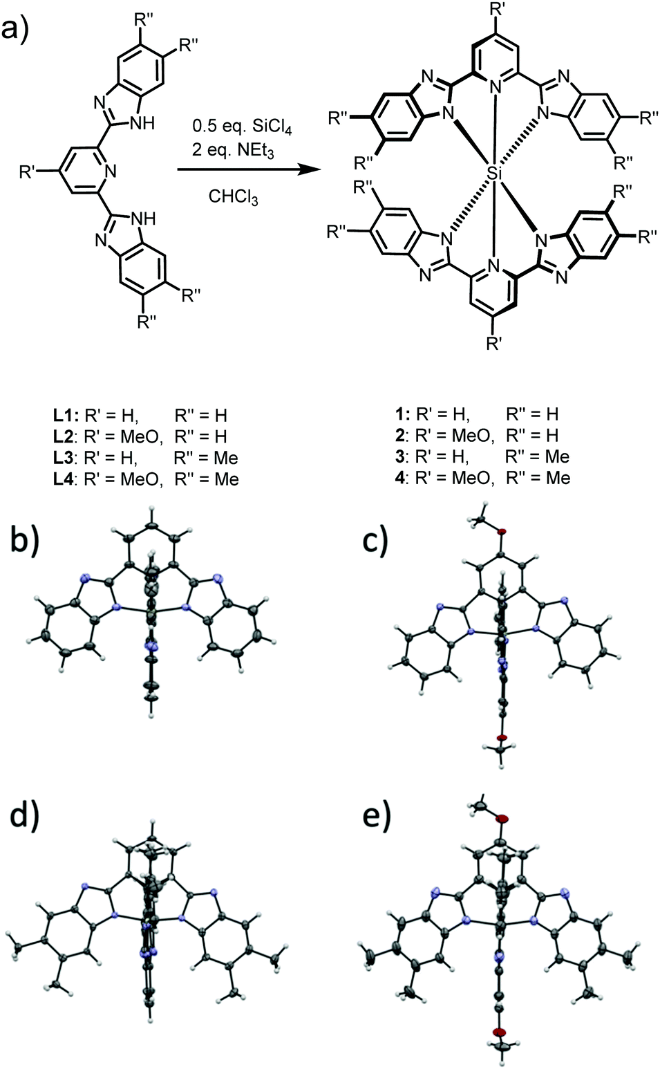 | ||
| Fig. 1 Synthesis (a) of complexes 1 – Si(bzimpy)2, 2 – Si(MeObzimpy)2, 3 – Si(Me2bzimpy)2, and 4 – Si(MeOMe2bzimpy)2, and crystal structures of 1 (b), 2 (c) 3 (d), and 4 (e). | ||
The rigid tridentate bzimpy pincer ligand affords Si(bzimpy) complexes excellent thermal stability. Thermogravimetric analyses under nitrogen shows stability over 400 °C for the methoxy-containing complexes, Si(MeObzimpy)2 and Si(MeOMe2bzimpy)2, over 500 °C for the parent Si(bzimpy)2, and 600 °C for the Si(Me2bzimpy)2 derivative (Fig. 2). The remarkable thermal stability of these materials allows them to be deposited using thermal evaporation, and makes them promising candidates as an active layer material for efficient molecular electronic devices.
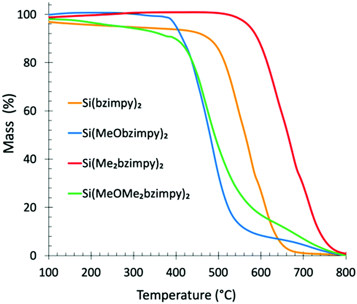 | ||
| Fig. 2 Thermogravimetric analysis of complexes (1–4) under nitrogen. | ||
Optical and electrochemical characterization
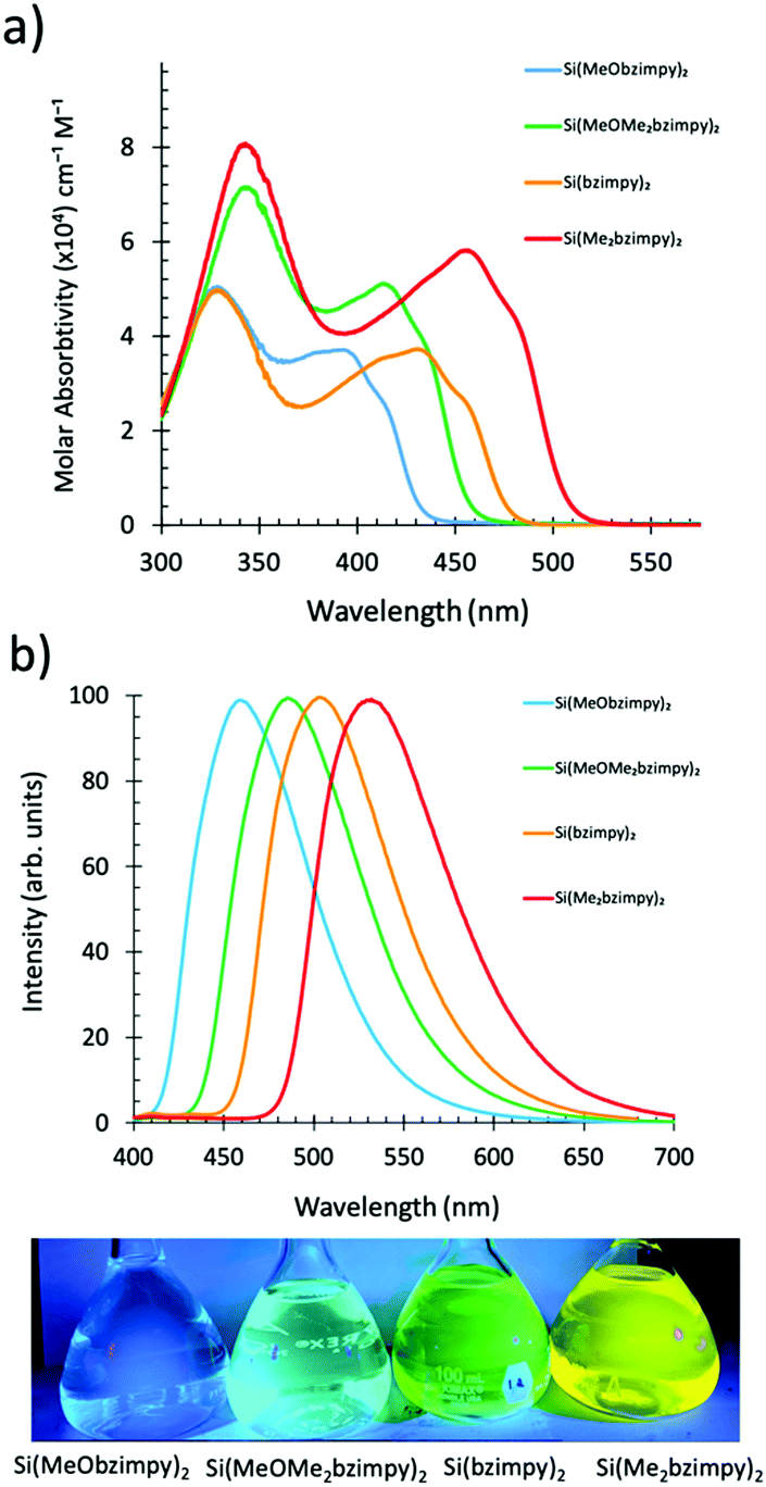
Solutions of Si(bzimpy)2 derivatives in dichloromethane show two UV-vis absorbance bands with the strongest transition between λmax = 325–350 nm and molar absorptivities ranging from 50![[thin space (1/6-em)]](https://www.rsc.org/images/entities/char_2009.gif) 000 to 80000 cm−1 M−1 (Fig. 3a). The lower energy S0–S1 singlet transition (π–π* transition) varied between λmax = 400–500 nm. The octamethylated, Si(Me2bzimpy)2 complex exhibited the lowest energy absorbance onset (ΔE), while the dimethoxy, Si(MeObzimpy)2 exhibited the largest. Calculated highest occupied molecular orbitals (HOMO) and lowest unoccupied molecular orbitals (LUMO) levels agree with this trend (Table 1). Electron density orbital maps show the HOMO delocalized predominantly over the benzimidazole portion of the complex ligands while the LUMO is spread over the pyridine moiety. Experimentally determined HOMO/LUMO values were obtained using cyclic voltammetry (reduction potentials) and the UV-vis absorption onset (ΔE) – (Table 1). Two semi-reversible reductions potentials were observed for each derivative (Fig. S2, ESI†). The addition of electron-donating methyl groups to the benzimidazole portion of the ligand raises the HOMO energy level, lowering the HOMO/LUMO gap (ΔE). The addition of the methoxy groups to the pyridine portion of the ligand raises the energy of the LUMO and results in a blue-shifted UV-vis spectrum and larger HOMO/LUMO gap (ΔE). The Si(bzimpy)2 parent compound and complex 4 containing the methoxy and methylated benzimidazole ligand, Si(MeOMe2bzimpy)2, exhibit an absorption range and (ΔE) in between complexes 2 and 3. The 29Si NMR peak also indicates an upfield shift (more electron shielding) in agreement with the overall electron donating ability of the substituents and the experimentally determined reduction potentials.
000 to 80000 cm−1 M−1 (Fig. 3a). The lower energy S0–S1 singlet transition (π–π* transition) varied between λmax = 400–500 nm. The octamethylated, Si(Me2bzimpy)2 complex exhibited the lowest energy absorbance onset (ΔE), while the dimethoxy, Si(MeObzimpy)2 exhibited the largest. Calculated highest occupied molecular orbitals (HOMO) and lowest unoccupied molecular orbitals (LUMO) levels agree with this trend (Table 1). Electron density orbital maps show the HOMO delocalized predominantly over the benzimidazole portion of the complex ligands while the LUMO is spread over the pyridine moiety. Experimentally determined HOMO/LUMO values were obtained using cyclic voltammetry (reduction potentials) and the UV-vis absorption onset (ΔE) – (Table 1). Two semi-reversible reductions potentials were observed for each derivative (Fig. S2, ESI†). The addition of electron-donating methyl groups to the benzimidazole portion of the ligand raises the HOMO energy level, lowering the HOMO/LUMO gap (ΔE). The addition of the methoxy groups to the pyridine portion of the ligand raises the energy of the LUMO and results in a blue-shifted UV-vis spectrum and larger HOMO/LUMO gap (ΔE). The Si(bzimpy)2 parent compound and complex 4 containing the methoxy and methylated benzimidazole ligand, Si(MeOMe2bzimpy)2, exhibit an absorption range and (ΔE) in between complexes 2 and 3. The 29Si NMR peak also indicates an upfield shift (more electron shielding) in agreement with the overall electron donating ability of the substituents and the experimentally determined reduction potentials.
 | ||
| Fig. 3 UV-vis absorption (a) and fluorescence emission spectra (b) with Si(bzimpy) complex solutions under UV light. | ||
| E red1 | ΔEUV-vis | E HOMO | ||||
|---|---|---|---|---|---|---|
| Complex | τ F (ns) | ϕ F | E red2 (V) | ΔEDFTc (eV) | E LUMO (eV) | 29Si (ppm) |
| a Lifetime and quantum yield determined in degassed CH2Cl2. b Potentials are referenced to ferrocene/ferrocenium. c Calculated in gas phase, B3LYP/6-31G*. d Calculated as EHOMO = ELUMO − ΔE(L–H),UV-vis. e Determined from cyclic voltammetry: ELUMO = −e[E(0/−1),onset + 4.8 V]. | ||||||
| 1 | 4.2 | 0.50 | −1.52 | 2.59 | −5.98 | −185.7 |
| −1.82 | 3.28 | −3.39 | ||||
| 2 | 3.3 | 0.63 | −1.79 | 2.86 | −5.95 | −187.4 |
| −2.06 | 3.54 | −3.09 | ||||
| 3 | 3.8 | 0.67 | −1.62 | 2.44 | −5.69 | −185.9 |
| −1.94 | 3.15 | −3.25 | ||||
| 4 | 4.1 | 0.66 | −1.85 | 2.71 | −5.79 | −188.5 |
| −2.07 | 3.42 | −3.08 | ||||
Singlet fluorescence emission spectra of the complexes in solution also show the HOMO/LUMO gap energy trend with a peak fluorescence range between 460 and 525 nm. This demonstrates the ability to easily tune the Si bzimpy pincer complexes to emit across a wide visible range (blue to yellow) through judicious substitution of electron-donating groups on either pyridine or benzimidazole moieties (Fig. 3b). The planarity and rigidity provided to the bzimpy ligand by the Si pincer structure results in enhanced singlet fluorescence quantum yields ΦF = 0.5–0.67 and lifetimes τF = 3.3–4.2 ns (Table 1 and Fig. S2, ESI†). Calculated radiative rates (krad = ΦF/τF) exhibited a narrow range between 1.2 × 10⁸ s−1 and 1.9 × 10⁸ s−1 for all investigated Si pincer complexes. Lastly, phosphorescence spectra were obtained by cooling dichloromethane solutions of each complex to 77 K, and observing phosphorescence emission several seconds after UV-LED light excitation (Fig. 4).
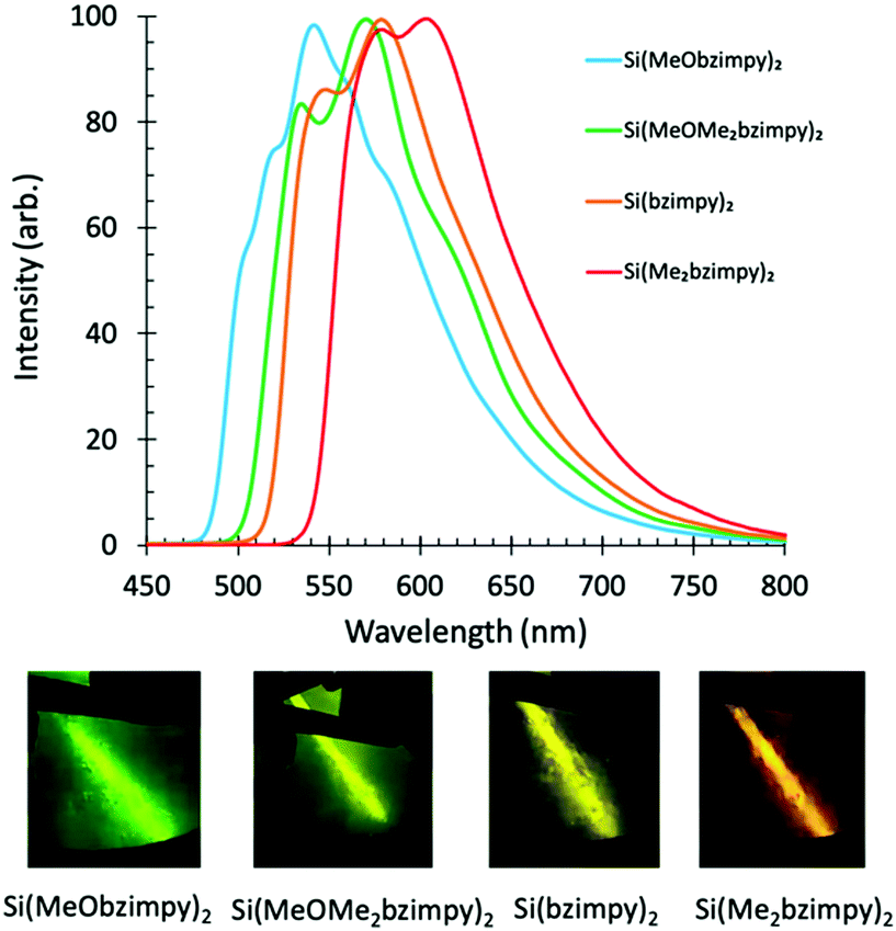 | ||
| Fig. 4 Phosphorescence spectra and optical images of complexes (1–4) in frozen dichloromethane (77 K) several seconds after UV excitation. | ||
Charge transport and device applications
Organic semiconducting materials have proven to be a disruptive technology due to their low cost, flexibility, and large area processibility. Measuring, optimizing, and establishing structure function relationships electron and hole mobilities is critical for designing efficient devices regardless of the organic material function. Organic semiconductors also find uses in a variety of OPV and OLED devices specifically as a hole conduction layer (HTL),28,29 or as the electron conduction layer (ETL).30 To demonstrate the full versatility of these complexes, devices incorporating the derivatives were constructed using vacuum-deposited thin films of the derivatives. We measured the electron and hole mobilities of the four Si(bzimpy)2 complexes using space charge limited current (SCLC). We also evaluated their application as the electroluminescent layer in an OLED device and as the electron transport layer an organic photovoltaic device.Electron and hole mobilities (μe and μh) of the complexes were measured in ITO/Si(bzimpy)2/Al or ITO/PEDOT:PSS/Si(bzimpy)2/Au sandwich configurations. The complexes were vacuum-deposited directly onto cleaned, patterned ITO substrates or PEDOT:PSS coated ITO substrates followed by metal cathode evaporation. Thin films of the materials exhibited similar surface roughness between 0.3–0.6 nm as measured by AFM (Fig. S3–S6, ESI†). Achievable film thicknesses and vacuum deposition rates varied for the Si(bzimpy)2 complexes. The methoxy-containing derivatives, Si(MeObzimpy)2 and Si(Me2OMebzimpy)2, were limited to deposition rates of ∼0.1 A s−1 and thicknesses between 14–35 nm. Whereas the Si(bzimpy)2 and Si(Me2bzimpy)2, could be deposited at higher rates (0.2–0.4) A s−1 and thicknesses ∼90 nm. The lower achievable film thicknesses and ease of vacuum deposition may be related to the lower thermal stability of the methoxy containing derivatives (Fig. 2). The as-deposited films showed amorphous characteristics as determined from powdered X-ray diffraction (p-XRD) studies of the thin films which indicate minimal crystallinity. Charge mobilities were calculated from the slopes of J vs. V2 curves fit to the Mott–Gurney equation. Plots of log(J) − log(V) showed linear behaviour with slopes consistent with a space charge limited current (SCLC) behaviour.31 The average electron and hole mobilities of the top three devices for each derivative are reported in Table 2.
| Complex | μ e (cm2 V−1 s−1) | μ h (cm2 V−1 s−1) |
|---|---|---|
| 1-Si(bzimpy)2 | 9.68 × 10⁻⁵ ± 5.49 × 10⁻⁵ | 5.31 × 10⁻⁶ ± 2.97 × 10⁻⁶ |
| 2-Si(MeObzimpy)2 | 2.51 × 10⁻⁸ ± 1.44 × 10⁻⁸ | 1.76 × 10⁻⁸ ± 5.45 × 10⁻⁹ |
| 3-Si(Me2bzimpy)2 | 2.94 × 10⁻⁵ ± 1.21 × 10⁻⁵ | 1.44 × 10⁻⁶ ± 1.75 × 10⁻⁷ |
| 4-Si(MeOMe2bzimpy)2 | 4.89 × 10⁻⁷ ± 3.98 × 10⁻⁷ | 3.19 × 10⁻⁸ ± 1.00 × 10⁻⁹ |
Electron and hole mobilities were highest for the parent complex, Si(bzimpy)2, (μe = 9.68 × 10⁻⁵ cm2 V−1 s−1, μh = 5.31 × 10⁻⁶ cm2 V−1 s−1) and were lowest for the methoxy-containing derivative Si(MeOMe2bzimpy)2, (μe = 2.51 × 10⁻⁸ cm2 V−1 s−1, μh = 1.76 × 10⁻⁸ cm2 V−1 s−1). The octamethylated complexes, Si(Me2bzimpy)2 and Si(MeOMe2bzimpy)2, also exhibited good charge mobilities ranging between 1.4 × 10⁻⁶–2.9 × 10⁻⁵ cm2 V−1 s−1. There are many considerations to account for the observed mobility variations including film quality from the thermal deposition, crystallinity, ohmic contact from the metal anode/cathodes, and molecular orientation within the films. Effective orbital overlap (HOMOs – hole transport) and (LUMOs – electron transport) due to molecular orientation induced by the addition of methyl/methoxy substituents can impact carrier transport.32 Thin film structural defects may also be present leading to larger trap state concentrations.33 Interestingly, all of the complexes studied showed relatively similar electron and hole mobilities suggesting their suitability as ambipolar charge transport layers or as host materials.32,34 These are encouraging results and demonstrate the clear multifunctional electronic nature of this class of molecular semiconductors.
Electroluminescence
Previously, we demonstrated electroluminescence of the parent compound in a simple two electrode OLED device structure.26 To further explore the unique electronic structure of the Si pincer complexes, OLED devices were constructed to probe both excitonic and excimeric emission. An excimer (exciplex or electroplex) is an excited state that forms between donor and acceptor material.35,36 This excited dimer results in emission that is lower in energy than emission from either monomeric species. We utilized the hole transport material, N,N′-di(1-naphthyl)-N,N′- diphenyl-(1,1′-biphenyl)-4,4′-diamine (NPB) whose HOMO level is higher than the Si pincer complexes to enable the observation the electroplex emission. We define this as electroplex emission, since emission was only observed through electroluminescence and not through photoexcitation.35 Devices were constructed with a MoO3 hole injection layer, the NPB hole transport layer, and the thermally evaporated Si(bzimpy)2 complex serving as both electron transport and electroluminescence layer. The devices were completed with a LiF buffer layer and Al cathode. Fig. 5a–d depicts a Si(bzimpy)2 device construction (ITO/MoO3/NPB/Si(bzimpy)2/LiF–Al) with energy level diagram, electroluminescence images from an encapsulated Si(bzimpy)2 device, and overlaid photoluminescence and electroluminescence emission spectra for each Si pincer complex.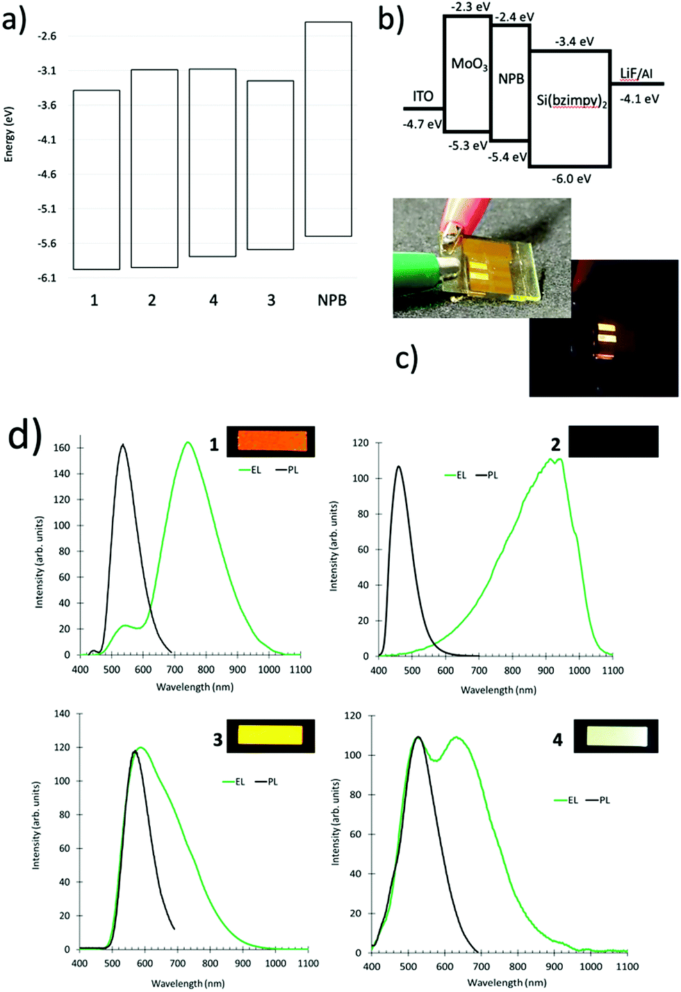 | ||
| Fig. 5 Si pincer complex energy level comparisons (a), Si(bzimpy)2 device construction with energy diagram (b), electroluminescence images (light and dark) from an encapsulated Si(bzimpy)2 device (c), and overlaid photoluminescence and electroluminescence emission spectra of each Si pincer complex (d). | ||
The electroluminescence data agrees well with the trend that a lower Si pincer HOMO level (more negative) leads to a larger electroplex (lower energy) emission contribution. Both Si(bzimpy)2 and Si(MeObzimpy)2 complexes show primarily an electroplex peak emission contribution between 750–930 nm and little or no excitonic emission at 540 nm. Both these complexes have the lowest HOMO levels (Table 1). Si(Me2bzimpy)2 has the highest HOMO level resulting in primarily excitonic peak emission and appears yellow (540 nm). Interestingly, the Si(MeOMe2bzimpy)2 devices exhibits nearly white electroluminescence with a relative equal mix of excitonic and electroplex emission. The electroplex emission varies considerably for each Si complex with the Si(MeObzimpy)2 exhibiting no visible emission. This is likely due to interfacial nature of the electroplex emission, and the electronic differences in the contact between the NPB hole transport layer and the Si pincer derivatives. These observations open up other possible opportunities for optimizing mixed excitonic/excimeric emissions tuning the electroluminescent emission wavelength.
Electron transport and buffer layer for OPVs
The promising charge transport properties of the Si(bzimpy)2 materials led us to examine these materials as an electron transport and buffer layer for organic photovoltaic devices (OPVs). Previous work using Alq3 as an electron transport material for a prototypical P3HT:PCBM device configuration showed strong improvements in fill factors (FF) and overall solar cell device performance.37,38 Both reports used Alq3 as an evaporated38 or solution-processed37 thin film inserted between the blended P3HT:PCBM photoactive region and the Al or Al/LiF cathode. The inserted layer improves the electron extraction efficiency and facilities electron transport within the solar cell device, resulting in improved short-circuit current densities (Jsc) and open-circuit voltage (Voc). We therefore constructed P3HT:PCBM organic solar cell devices and tested their performance with and without an evaporated Si pincer electron transport layer between the active layer and Al metal contact. All four Si(bzimpy)2 complexes were evaluated in an OPV device through deposition as thin films on the active photovoltaic region of the device (structure ITO/PEDOT:PSS/P3HT:PCBM/Si(bzimpy)2/Al) with thicknesses ranging between 3–4.5 nm. A summary of the resulting solar cell device properties is listed in Table 3 with JV curves of the devices with the various derivatives in Fig. 6.| OPV Devices w/ETL Layer | V oc (V) | J sc (mA cm−2) | FF | η (%) |
|---|---|---|---|---|
| No ETL layer | 0.52 ± 0.02 | 13.2 ± 0.8 | 0.42 ± 0.02 | 2.87 ± 0.06 |
| 1-Si(bzimpy)2 | 0.59 ± 0.01 | 13.7 ± 0.2 | 0.53 ± 0.003 | 4.32 ± 0.15 |
| 2-Si(MeObzimpy)2 | 0.59 ± 0.01 | 12.6 ± 0.8 | 0.48 ± 0.005 | 3.55 ± 0.21 |
| 3-Si(Me2bzimpy)2 | 0.61 ± 0.01 | 14.6 ± 1.2 | 0.51 ± 0.014 | 4.54 ± 0.34 |
| 4-Si(MeOMe2bzimpy)2 | 0.61 ± 0.01 | 13.3 ± 2.4 | 0.53 ± 0.033 | 4.27 ± 0.51 |
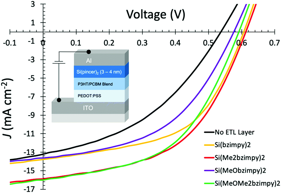 | ||
| Fig. 6 Representative J–V measurement curves (with device structure inset image) of P3HT:PCBM OPV devices under 100 mW cm−2 illumination with various Si(pincer)2 electron transport layers (3–4 nm). | ||
Data from the P3HT:PCBM device summary and JV curves (Table 3 and Fig. 6) consistently show an overall solar cell device improvement in the performance over the control device that contained no additional electron transport layer. All four complexes showed an enhancement in the Voc, Jsc, FF, and therefore overall solar conversion efficiency (η). The largest efficiency improvement was seen when using Si(Me2bzimpy)2 as an electron transport and buffer layer which resulted in an average device improvement of 50% compared to the controlled devices with no deposited Si(pincer)2 layer (η = 2.87 improved to η = 4.54%). Similar improvements were seen with Si(Me2bzimpy)2 and Si(MeOMe2bzimpy)2 devices with the smallest increase observed with the Si(MeObzimpy)2 derivative. The fill factors (FF) and open-circuit voltages (Voc) improved for all the devices containing an evaporated Si(pincer)2 complexes, a good indication of an improved electronic contact between the Al cathode and blended polymer/PCBM photoactive layer. The lowered contact resistance demonstrates the ability of these materials to increase open-circuit voltages, presumably through a more ohmic, interfacial contact.38 The thermally stable, evaporated Si(pincer)2 layer may also provide protection to the photoactive P3HT:PCBM layer from the aluminium metal cathode deposition.
Conclusions
Si(bzimpy)2, Si(MeObzimpy)2, Si(Me2bzimpy)2, and Si(MeOMe2bzimpy)2 complexes were synthesized, characterized, and evaluated in a variety of molecular electronic device architectures. The rigid tridentate pincer complexes show excellent thermal stability, strong fluorescence, and promising electron/hole (ambipolar) charge-carrier properties. Electroluminescent OLED devices were constructed to probe both excitonic and excimeric emission, which demonstrated the ability to tune the Si(pincer)2 electronic structure through a combination of methyl and methoxy groups placed judiciously around the bzimpy ligand. Lastly, organic (P3HT:PCBM) photovoltaic devices were constructed and tested using a thin layer of the Si(pincer)2 materials as an electron transport/buffer layer. Overall organic solar cell device performances improved for all devices that incorporated the thermally deposited Si(pincer)2 thin film to improve the electronic contact between the photoactive region and metal cathode. The molecular properties and promising electronic device performance, provide strong evidence of the usefulness of this class of hexacoordinate silicon complexes for future optoelectronic device applications.Conflicts of interest
A patent application covering the application of Si(pincer)2 compounds for electronic device applications has been filed by UNC Charlotte. Light and Charge Solutions, LLC DBA Margik is working with UNC Charlotte to explore commercialization of the technology.Acknowledgements
Funding was provided by the National Science Foundation Division of Chemistry award number CHE-1800331.Notes and references
- J. Song, H. Lee, E. G. Jeong, K. C. Choi and S. Yoo, Organic Light-Emitting Diodes: Pushing Toward the Limits and Beyond, Adv. Mater., 2020, 32(35), 1907539 CrossRef CAS PubMed.
- Q. Zhang, B. Li, S. Huang, H. Nomura, H. Tanaka and C. Adachi, Efficient blue organic light-emitting diodes employing thermally activated delayed fluorescence, Nat. Photonics, 2014, 8(4), 326–332 CrossRef CAS.
- Q. Zhang, J. Li, K. Shizu, S. Huang, S. Hirata, H. Miyazaki and C. Adachi, Design of Efficient Thermally Activated Delayed Fluorescence Materials for Pure Blue Organic Light Emitting Diodes, J. Am. Chem. Soc., 2012, 134(36), 14706–14709 CrossRef CAS PubMed.
- N. A. Kukhta, T. Matulaitis, D. Volyniuk, K. Ivaniuk, P. Turyk, P. Stakhira, J. V. Grazulevicius and A. P. Monkman, Deep-Blue High-Efficiency TTA OLED Using Para- and Meta-Conjugated Cyanotriphenylbenzene and Carbazole Derivatives as Emitter and Host, J. Phys. Chem. Lett., 2017, 8(24), 6199–6205 CrossRef CAS PubMed.
- N. B. Kotadiya, P. W. M. Blom and G.-J. A. H. Wetzelaer, Efficient and stable single-layer organic light-emitting diodes based on thermally activated delayed fluorescence, Nat. Photonics, 2019, 13(11), 765–769 CrossRef CAS.
- A. Kojima, K. Teshima, Y. Shirai and T. Miyasaka, Organometal Halide Perovskites as Visible-Light Sensitizers for Photovoltaic Cells, J. Am. Chem. Soc., 2009, 131(17), 6050–6051 CrossRef CAS PubMed.
- S. A. Wolf, D. D. Awschalom, R. A. Buhrman, J. M. Daughton, S. von Molnár, M. L. Roukes, A. Y. Chtchelkanova and D. M. Treger, Spintronics: A Spin-Based Electronics Vision for the Future, Science, 2001, 294(5546), 1488 CrossRef CAS PubMed.
- Z. H. Xiong, D. Wu, Z. Valy Vardeny and J. Shi, Giant magnetoresistance in organic spin-valves, Nature, 2004, 427(6977), 821–824 CrossRef CAS PubMed.
- C. W. Tang and S. A. VanSlyke, Organic electroluminescent diodes, Appl. Phys. Lett., 1987, 51(12), 913–915 CrossRef CAS.
- H. Liu, Z. Ma, R. Yu, H. Gao, J. Lin, T. Hayat, A. Alsaedi and Z. a. Tan, Crosslinkable metal chelate as the electron transport layer for efficient and stable inverted polymer solar cells, Mater. Chem. Front., 2020, 4(10), 2995–3002 RSC.
- C. H. Chen and J. Shi, Metal chelates as emitting materials for organic electroluminescence, Coord. Chem. Rev., 1998, 171, 161–174 CrossRef CAS.
- S.-H. Liao, J.-R. Shiu, S.-W. Liu, S.-J. Yeh, Y.-H. Chen, C.-T. Chen, T. J. Chow and C.-I. Wu, Hydroxynaphthyridine-Derived Group III Metal Chelates: Wide Band Gap and Deep Blue Analogues of Green Alq3 (Tris(8-hydroxyquinolate)aluminum) and Their Versatile Applications for Organic Light-Emitting Diodes, J. Am. Chem. Soc., 2009, 131(2), 763–777 CrossRef CAS PubMed.
- A. Tsuboyama, H. Iwawaki, M. Furugori, T. Mukaide, J. Kamatani, S. Igawa, T. Moriyama, S. Miura, T. Takiguchi, S. Okada, M. Hoshino and K. Ueno, Homoleptic Cyclometalated Iridium Complexes with Highly Efficient Red Phosphorescence and Application to Organic Light-Emitting Diode, J. Am. Chem. Soc., 2003, 125(42), 12971–12979 CrossRef CAS PubMed.
- R. C. Evans, P. Douglas and C. J. Winscom, Coordination complexes exhibiting room-temperature phosphorescence: Evaluation of their suitability as triplet emitters in organic light emitting diodes, Coord. Chem. Rev., 2006, 250(15), 2093–2126 CrossRef CAS.
- H. Yersin, A. F. Rausch, R. Czerwieniec, T. Hofbeck and T. Fischer, The triplet state of organo-transition metal compounds. Triplet harvesting and singlet harvesting for efficient OLEDs, Coord. Chem. Rev., 2011, 255(21), 2622–2652 CrossRef CAS.
- J. Ohshita, Conjugated Oligomers and Polymers Containing Dithienosilole Units, Macromol. Chem. Phys., 2009, 210(17), 1360–1370 CrossRef CAS.
- L. Chen, Y. Jiang, H. Nie, P. Lu, H. H. Y. Sung, I. D. Williams, H. S. Kwok, F. Huang, A. Qin, Z. Zhao and B. Z. Tang, Creation of Bifunctional Materials: Improve Electron-Transporting Ability of Light Emitters Based on AIE-Active 2,3,4,5-Tetraphenylsiloles, Adv. Funct. Mater., 2014, 24(23), 3621–3630 CrossRef CAS.
- J. Yang, N. Sun, J. Huang, Q. Li, Q. Peng, X. Tang, Y. Dong, D. Ma and Z. Li, New AIEgens containing tetraphenylethene and silole moieties: tunable intramolecular conjugation, aggregation-induced emission characteristics and good device performance, J. Mater. Chem. C, 2015, 3(11), 2624–2631 RSC.
- S. A. Ponomarenko and S. Kirchmeyer, Conjugated Organosilicon Materials for Organic Electronics and Photonics, in Silicon Polymers, ed. Muzafarov, A. M., Springer Berlin Heidelberg, Berlin, Heidelberg, 2011, pp. 33–110 Search PubMed.
- A. J. Pearson, T. Plint, S. T. E. Jones, B. H. Lessard, D. Credgington, T. P. Bender and N. C. Greenham, Silicon phthalocyanines as dopant red emitters for efficient solution processed OLEDs, J. Mater. Chem. C, 2017, 5(48), 12688–12698 RSC.
- T. Plint, B. H. Lessard and T. P. Bender, Assessing the potential of group 13 and 14 metal/metalloid phthalocyanines as hole transport layers in organic light emitting diodes, J. Appl. Phys., 2016, 119(14), 145502 CrossRef.
- B. H. Lessard, J. D. Dang, T. M. Grant, D. Gao, D. S. Seferos and T. P. Bender, Bis(tri-n-hexylsilyl oxide) Silicon Phthalocyanine: A Unique Additive in Ternary Bulk Heterojunction Organic Photovoltaic Devices, ACS Appl. Mater. Interfaces, 2014, 6(17), 15040–15051 CrossRef CAS PubMed.
- B. H. Lessard, R. T. White, M. Al-Amar, T. Plint, J. S. Castrucci, D. S. Josey, Z.-H. Lu and T. P. Bender, Assessing the Potential Roles of Silicon and Germanium Phthalocyanines in Planar Heterojunction Organic Photovoltaic Devices and How Pentafluoro Phenoxylation Can Enhance π–π Interactions and Device Performance, ACS Appl. Mater. Interfaces, 2015, 7(9), 5076–5088 CrossRef CAS PubMed.
- J. Liu, X. Yang and L. Sun, Axial anchoring designed silicon–porphyrin sensitizers for efficient dye-sensitized solar cells, Chem. Commun., 2013, 49(100), 11785–11787 RSC.
- D. M. Peloquin and T. A. Schmedake, Recent advances in hexacoordinate silicon with pyridine-containing ligands: Chemistry and emerging applications, Coord. Chem. Rev., 2016, 323, 107–119 CrossRef CAS.
- M. Kocherga, J. Castaneda, M. G. Walter, Y. Zhang, N.-A. Saleh, L. Wang, D. S. Jones, J. Merkert, B. Donovan-Merkert, Y. Li, T. Hofmann and T. A. Schmedake, Si(bzimpy)2 – a hexacoordinate silicon pincer complex for electron transport and electroluminescence, Chem. Commun., 2018, 54(100), 14073–14076 RSC.
- S. Günnaz, A. G. Gökçe and H. Türkmen, Synthesis of bimetallic complexes bridged by 2,6-bis(benzimidazol-2-yl) pyridine derivatives and their catalytic properties in transfer hydrogenation, Dalton Trans., 2018, 47(48), 17317–17328 RSC.
- H. Xu, H. Zou, D. Zhou, G. Zeng, L. Chen, X. Liao and Y. Chen, Printable Hole Transport Layer for 1.0 cm2 Organic Solar Cells, ACS Appl. Mater. Interfaces, 2020, 12(46), 52028–52037 CrossRef CAS PubMed.
- S. Kang, R. Jillella, J. Jeong, Y.-I. Park, Y.-J. Pu and J. Park, Improved Electroluminescence Performance of Perovskite Light-Emitting Diodes by a New Hole Transporting Polymer Based on the Benzocarbazole Moiety, ACS Appl. Mater. Interfaces, 2020, 12(46), 51756–51765 CrossRef CAS PubMed.
- J.-H. Kim and J.-W. Park, Designing an electron-transport layer for highly efficient, reliable, and solution-processed organic light-emitting diodes, J. Mater. Chem. C, 2017, 5(12), 3097–3106 RSC.
- V. Coropceanu, J. Cornil, D. A. da Silva Filho, Y. Olivier, R. Silbey and J.-L. Brédas, Charge Transport in Organic Semiconductors, Chem. Rev., 2007, 107(4), 926–952 CrossRef CAS PubMed.
- J. Zaumseil and H. Sirringhaus, Electron and Ambipolar Transport in Organic Field-Effect Transistors, Chem. Rev., 2007, 107(4), 1296–1323 CrossRef CAS PubMed.
- H. F. Haneef, A. M. Zeidell and O. D. Jurchescu, Charge carrier traps in organic semiconductors: a review on the underlying physics and impact on electronic devices, J. Mater. Chem. C, 2020, 8(3), 759–787 RSC.
- K. Zhou, H. Dong, H.-l. Zhang and W. Hu, High performance n-type and ambipolar small organic semiconductors for organic thin film transistors, Phys. Chem. Chem. Phys., 2014, 16(41), 22448–22457 RSC.
- P. Xiao, J. Huang, Y. Yu, J. Yuan, D. Luo, B. Liu and D. Liang, Recent Advances of Exciplex-Based White Organic Light-Emitting Diodes, Appl. Sci., 2018, 8(9), 1449 CrossRef.
- Z. Zhao, B. Xu, Z. Yang, H. Wang, X. Wang, P. Lu and W. Tian, White Light from Excimer and Electromer in Single-Emitting-Component Electroluminescent Diodes, J. Phys. Chem. C, 2008, 112(23), 8511–8515 CrossRef CAS.
- B. Y. Kadem, A. K. Hassan and W. Cranton, Enhancement of power conversion efficiency of P3HT:PCBM solar cell using solution processed Alq3 film as electron transport layer, J. Mater. Sci.: Mater. Electron., 2015, 26(6), 3976–3983 CrossRef CAS.
- J. Y. Lee, T. Lee, H. J. Park and L. J. Guo, Improved solar cell performance by adding ultra-thin Alq3 at the cathode interface, Org. Electron., 2014, 15(11), 2710–2714 CrossRef CAS.
Footnote |
| † Electronic supplementary information (ESI) available. CCDC 2056293, 2049551 and 2049366. For ESI and crystallographic data in CIF or other electronic format see DOI: 10.1039/d1ma00737h |
| This journal is © The Royal Society of Chemistry 2022 |