
 Open Access Article
 This Open Access Article is licensed under a Creative Commons Attribution-Non Commercial 3.0 Unported Licence
Functionally graded magnetodielectric composite substrates for massive miniaturization of microstrip antennas†
Deepa Rajendran
Lekshmi
ab,
Sivan Pillai
Adarsh
ab,
Manikanta
Bayal
c,
Swapna Shanmukhan
Nair
 c and
Kuzhichalil Peethambharan
Surendran
*ab
c and
Kuzhichalil Peethambharan
Surendran
*ab
aMaterials Science and Technology Division, CSIR-National Institute for Interdisciplinary Science and Technology, Industrial Estate, Thiruvananthapuram – 695 019, Kerala, India. E-mail: kpsurendran@niist.res.in; Fax: +91-471-2491712; Tel: +91-471-2515474 Tel: +91-471-2515258
bAcademy of Scientific and Innovative Research (AcSIR), Ghaziabad, Uttar Pradesh – 201 002, India
cDepartment of Physics, Central University of Kerala, Thejaswini Hills, Periye, Kasaragod – 671316, India
First published on 2nd February 2022
Abstract
In the present work, an axially anisotropic magnetodielectric composite, based on polymethyl methacrylate (PMMA)–NiFe2O4 (NFO), was designed for realizing miniaturized antennas. The structural as well as ferromagnetic properties of the developed NiFe2O4via a polymer pyrolysis method were studied in detail. Thin sheets of (0–3) composites were developed by adding a different volume % of NFO (5, 10, 15, and 20 vol%) in the PMMA matrix. Structural, dielectric, magnetic and magnetocapacitance measurements were investigated for individual composites. A microstrip patch antenna operating at 830 MHz was theoretically modeled by stacking differently loaded MD wafers to form a functionally graded anisotropic composite, to be used as the antenna substrate. An impressive miniaturization of 95.46% was observed for this MD antenna, when compared to normal dielectric substrates with permittivity and permeability values equal to unity.
Introduction
Over the past few decades, researchers in the domain of condensed matter physics have redirected their attention to multifunctional materials that can meet the challenges of massive scaling in electronic devices. Multiferroic materials simultaneously possess multiple ferroic orders such as ferroelectricity, ferromagnetism and ferroelasticity.1 These materials are always being scrutinized for developing filters, data storage devices, phase shifters, etc.2 There are certain classes of multiferroic materials in which coexistence of ferromagnetic and ferroelectric behaviours gives rise to new combinations of properties like a magnetodielectric effect, magnetoelectric effect, etc. In magnetodielectric materials, dielectric properties can be controlled using a magnetic field, which qualifies them for scores of applications in antenna miniaturization, information storage, spintronics, etc.3–5 In many wireless communication systems including microstrip antennas, appreciable size reduction can be successfully achieved by choosing a high permittivity material as the antenna substrate. However, mainly there are two disadvantages for high permittivity substrates: (i) excitation of surface waves and strong capacitative coupling between the high permittivity substrate and base plane that will diminish the radiation performance and bandwidth of the antenna, and (ii) the characteristic impedance of the high permittivity substrate is low which may create difficulties in impedance matching between the device and free space. The best alternative is to choose a magnetodielectric material as the substrate, with moderate values of relative permittivity (εr) and permeability (μr). Magnetodielectric (MD) materials are a class of multifunctional composite dielectrics with magnetic particles as the filler. In such systems, the dielectric properties will vary under the application of magnetic field, thereby enabling simultaneous ease of impedance matching and miniaturization in patch antennas. Here a high miniaturization factor can be reached while diminishing the strong capacitative coupling between the antenna and ground plane. In this way, the capacitive nature of the resonant patch antenna is mitigated by inductance that can further counteract the former, thereby improving both the bandwidth and efficiency of the microstrip patch antenna.6
Tuning the dielectric properties of a material under the application of a magnetic field has been both scientifically admissible and technologically demanding.7 Two main strategies to magnetically control the dielectric or capacitive property of a material are, (a) controlling the interface physics in multilayer systems and (b) amplifying the magnetodielectric effect in ferromagnetic materials near its ferromagnetic transitions.8,9 Usually single phase magnetodielectrics possess a weak magnetodielectric effect (MDE) at room temperature due to crystal symmetry restrictions, which will further restrict such a material's implementation in technological applications.10 It is well known that a combination of two materials that have excellent electronic properties will give rise to new composites of great technological interest. The desired electronic property of the resultant composite material can be synergically improved by the addition of a second phase.11,12 Likewise, combining materials with promising dielectric and magnetic properties is a candid approach to generate a large MDE near room temperature.13,14 The two main mechanisms that lead to a large MDE in composite materials are given below.15,16
(i) A combination of magnetoresistance (MR) and Maxwell–Wagner effects.
(ii) Magnetic field induced strain transfer through interface coupling.
In the first case, the selection of materials for MR related MDE is broad.17 But in the latter case, a magnetic and dielectric material coexists in the system obeying the principles of composites. When a magnetic field is applied to MDs, a strain will be induced in the magnetostrictive phase of the composite. This generated stress at the interface can induce dielectric polarization in the respective component of the composite system, which will result in a strong MDE response.18,19
Generally, ceramic based materials are used for developing MD composites, but they possess several disadvantages. Primarily, ceramic MDs require high temperature processing. On top of this, the poor machinability of ceramics causes difficulties in designing components of the desired shape. These problems can be circumvented by using polymer-based composites by filling dielectric polymers with magnetic components. They possess advantages of low temperature processing, a wide range of versatilities, low costs, a high dielectric break down field, etc.20 Following this, efforts have been made by researchers to develop polymer nanocomposites because of their synergic and tunable properties.5,20–23 Several researchers have reported new composites with attractive electronic properties by combining different types of polymers with magnetodielectric oxides.24,25 Against this background, the present work explores the viability of developing a functionally gradient polymer nanocomposite based MD substrate for antenna miniaturization.
Here, PMMA was used as the dielectric component, which is one of the major functional polymers that has a low dielectric loss over a wide frequency range at room temperature.26–28 Among various magnetic fillers, soft spinel ferrites (M2+Fe3+2O4) (M = Co, Ni, Zn, Mn etc.) exhibit impressive saturation magnetization, low Eddy current loss as well as high electrical conductivity, making them suitable for high frequency applications.29–31 In addition to the resurged interest of spinel ferrites in the telecommunication industry, they find new applications in biomedical engineering,32,33 electromagnetism,34 and also as electrode materials in Li-ion batteries35etc. The chosen ferrite, NiFe2O4, has an inverse spinel structure with an AB2O4 crystal structure. It shows ferrimagnetism that originates from the magnetic moment of anti-parallel spins between Fe3+ ions at the tetrahedral sites and Ni2+ ions at the octahedral sites, formed by cubic close packing of oxygen (O2−) ions.36 The present work focuses on developing a (0–3) composite based on PMMA–NiFe2O4 with various magnetic filler loading. However, a thoroughly isotropic MD substrate may compromise the bandwidth, gain and return loss of the microstrip patch antenna. One way to address this issue is to design axially anisotropic substrates. Usually, the development of substrates with in-plane (x–y) isotropy but that are anisotropic along the z axis, is an engineering challenge, which has been realized in this work for the first time. Herein, the axially anisotropic MD substrate was developed by stacking the developed (0–3) composite, which is ideal for antenna miniaturization applications and furthermore, its practical feasibility is modelled using a finite element method solver, HFSS.
Experimental section
Materials
Nickel nitrate (Ni(NO3)2·6H2O, Sigma Aldrich), iron nitrate (Fe(NO3)3·9H2O, Sigma Aldrich), ammonium persulfate ((NH4)2S2O8, Sigma Aldrich), acrylic acid (C2H2O2, Sigma Aldrich), polymethyl methacrylate (PMMA, Sigma Aldrich), and N,N-dimethylformamide (DMF, HPLC) were used.Synthesis of NFO
There have been many novel techniques developed by researchers for synthesizing functional oxides and ferrites for practical applications.37,38 In the present study, a polymer pyrolysis method was employed to synthesise NFO nanoparticles. This method possesses so many advantages when compared to other wet chemical synthesis procedures, including easy operation, scaling up in the form of batch and the production of highly homogeneous nanocrystalline spinel ferrites. NiFe2O4 with a well-defined structure was prepared by pyrolysis of Ni–Fe polyacrylate precursors, via in situ polymerization.Chemical reagents such as Ni(NO3)2·6H2O, Fe(NO3)3·9H2O, (NH4)2S2O8 and C2H2O2 were used without further purification. Initially, ferric nitrate and nickel salt were dissolved in 10 g of acrylic acid aqueous solution with acrylic acid![[thin space (1/6-em)]](https://www.rsc.org/images/entities/char_2009.gif) :H2O =70:30 wt%, under constant stirring. Then, 0.5 g of the initiator ((NH4)2S2O8) was added to the mixed solution in order to promote polymerization. The mixed solution was kept at 70 °C under constant stirring for 2 h to form a well distributed polyacrylate salt. The as-obtained polyacrylate was kept in an oven at 100 °C for 24 h. After drying, it was taken to calcination at different temperatures in a furnace, in an O2 atmosphere.
:H2O =70:30 wt%, under constant stirring. Then, 0.5 g of the initiator ((NH4)2S2O8) was added to the mixed solution in order to promote polymerization. The mixed solution was kept at 70 °C under constant stirring for 2 h to form a well distributed polyacrylate salt. The as-obtained polyacrylate was kept in an oven at 100 °C for 24 h. After drying, it was taken to calcination at different temperatures in a furnace, in an O2 atmosphere.
Synthesis of PMMA–NFO composites
The polymer nanocomposites were synthesized through an in situ method. Initially, PMMA was dissolved in DMF under continuous sonication. At the same time, the required amount of NFO was sonicated in DMF. After complete dissolution, both the filler and matrix were mixed together in an ultrasonicator for many hours. Finally, the composite was precipitated out from DMF by filtration and dried in a hot air oven for 12 h. A series of composites was developed using this technique, namely NFO5 (5 vol% NFO/0.05 Vf NFO), NFO10 (10 vol% NFO/0.1 Vf NFO), NFO15 (15 vol% NFO/0.15 Vf NFO) and NFO20 (20 vol% NFO/0.2 Vf NFO). Various characterizations were performed using samples developed through a hot-pressing technique.Characterization
Thermogravimetry/differential thermal analysis (TG/DTA) of the Ni–Fe precursor powder was carried out from room temperature up to 600 °C in an air atmosphere using a thermogravimetric analyzer (TGA/DTA instrument, Shimadzu, Japan) at a rate of 10 °C min−1. The phase purity of the calcined powders at different temperatures was analyzed using X-ray diffraction (XRD) analysis with Cu Kα radiation (X’Pert PRO diffractometer, PANalytical, Almelo, The Netherlands). The particle size of the calcined NFO was characterized using high-resolution transmission electron microscopy (HRTEM) (FEI Tecnai G2 30S-TWIN, FEI Co., Hillsboro, OR, USA) by drop casting it in ethanol medium. The magnetic properties of NFO as well as the composites developed were measured using a oven measurement attached to a Physical Property Measurement System (PPMS, Quantum Design, San Diego, CA, USA). Wide angle XRD (WAXD) was used for characterizing the phase formation of PMMA and NFO loaded samples using a Genix micro source (Xenocs, Grenoble, France) operated at 50 kV and 0.6 mA. Similar to the XRD analysis, Cu Kα radiation (λ = 1.54 Å) was also used here. To understand the thermal stability of PMMA and its composites, TG analysis was performed using the thermogravimetric analyzer TA Q50 under a N2 atmosphere, at a heating rate of 10 °C min−1. Thermal conductivity of the samples was measured using a laser flash thermal property analyzer, Flash Line 2000 (Anter corporation, Pittsburgh, PA, USA). A thermomechanical analyzer (TMA/SS7300, SII NanoTechnology Inc., Tokyo, Japan) was used for characterizing the coefficient of thermal expansion for all the samples from room temperature to 80 °C under the application of 0.1 N force. Microstructural analysis was performed for the fractured surface of the composites using an EDS coupled SEM, Zeiss EVO 18 Cryo SEM (Carl Zeiss AG, Oberkochen Germany). The magnetocapacitance (MC) measurements were obtained using an Impedance Analyzer (Model 6500B Wayne Kerr, West Sussex, UK). The theoretical simulation of the proposed antenna was done using Ansys High Frequency Structure Simulator (HFSS) software.Results and discussion
The thermal evolution of the chemically derived NFO precursor was performed using DTA/TGA, prior to their calcination in the temperature range of 350–550 °C for 4 h. Fig. 1(a) represents the DTA/TG curve of the co-polymeric Ni–Fe precursors. A small weight loss of 6% occurs up to 100 °C, which corresponds to the removal of planar water from the powder. A minor endothermic peak is observed at 283 °C corresponding to a weight loss of 25% between 100–300 °C, which is due to the elimination of residual solvents in the precursor. A major weight loss of around 53% is observed between the temperature range of 300 °C to 420 °C and the sharp endothermic peak at 389 °C corresponds to the same. This can be attributed to the thermal decomposition of polymer chains and nitrates to form oxides.39 | ||
| Fig. 1 (a) TG/DTA of the prepared NFO precursor powder and (b) the XRD pattern of NFO calcined at different temperatures for 4 h. | ||
Fig. 1(b) represents the XRD of NFO calcined at various temperatures ranging from 350–550 °C for 4 h. The peak intensity increases with an increase in calcination temperature. The diffraction pattern obtained at 550 °C matches well with JCPDS file number 86-2267. Calcining at temperature ≥550 °C shows the sign of single phase spinel ferrite formation, without any impurity phase.
The microstructure of the crystallized powder was characterized using TEM and is shown in Fig. 2(a). It is found that particles are possessing nanometric scale morphology ranging from 20–50 nm. In order to elucidate the magnetic behavior of synthesized NFO in an accurate manner, the variation in magnetization with respect to the magnetic field was studied at various temperatures ranging from 300 K to 900 K. The result is presented in Fig. 2(b). The M–H curve at 900 K shows negligible values for remanence and coercivity, that suggest the paramagnetic behavior of developed nanocrystalline NFO particles, at a temperature above TC. The saturation magnetization (Ms) at 300 K is around 48 emu g−1 which is lower when compared to that of bulk NFO.40,41 A decrease in the average crystalline size has a considerable effect on the magnetic and electrical properties of materials.42,43 As the temperature increases from 300 K to 900 K, the saturation magnetization decreases and at 900 K, it became zero (paramagnetic). The magnetization vs. temperature (M–T) plot gives an insight into the ferromagnetic Curie temperature of a material.
 | ||
| Fig. 2 (a) TEM micrograph of NFO calcined at 550 °C, (b) M–H curves for NFO taken at different temperatures, (c) ZFC and FC curves taken at 50 Oe and (d) dM/dT plot showing the Curie transition temperature (TC) of the developed NFO powder. | ||
The M–T plot of NFO at 50 Oe is presented in Fig. 2(c). When the applied field is less, all the spins may not align in the direction of the applied field, which will result in bifurcation in zero field cooled (ZFC) and field cooled (FC) curves. The point at which ZFC meets FC is obviously the Curie temperature (TC). For accurately determining the TC value, dM/dT is plotted against temperature for the ZFC curve, as shown in Fig. 2(d). The transition from a ferromagnetic to paramagnetic nature is indicated by the sharp decrease in magnetization in this figure. The Curie temperature of NFO is found to be 840 K, which is in good agreement with the previously reported values.44
After ascertaining the structural, thermal, and magnetic properties of pristine NFO powder, its composites with PMMA were developed. Four composites namely, NFO5, NFO10, NFO15 and NFO20 were used to determine their suitability for application in the field of antenna miniaturization. Fig. S1(a) (ESI†) represents the WAXD of pristine PMMA and its composites. While scanning through the image, it is seen that PMMA is amorphous in nature. When the NFO content in the composite is increased from 5 vol% to 20 vol%, the intensity of PMMA starts diminishing and a peak at 31.5° starts appearing. This peak corresponds to the (220) plane of NFO which is consistent with Fig. 1(b). Fig. S1(b) (ESI†) shows the TGA thermograms for the samples. The TGA plot reveals the enhancement in thermal stability of the developed composites when compared to the pure polymer. This plot clearly indicates that the decomposition temperature of the composites has progressively improved as a function of NFO content. At the 50% weight loss temperature, there is an enhancement of 35 °C in the decomposition temperature of NFO20 when compared to pristine PMMA. This is due to the presence of the high thermal conducting material NFO which results in the formation of carbonaceous char that will further act as a barrier for mass transport and will delay the decomposition process in composites.45
Fig. 3(a) represents the magnetic characterization of PMMA–NFO composites. The M–H curve indicates that when the NFO content increases, the saturation magnetization (Ms) also increases due to obvious reasons.
 | ||
| Fig. 3 (a) M–H curves for the developed composites compared with that of pristine NFO powder, and (b) variation in thermal conductivity with respect to filler loading. | ||
Table S1 (ESI†) shows the values of Ms and remanent magnetization (Mr) of the composites and pure NFO. When compared to pure NFO, the Ms value of the composites is lower which is due to the presence of polymeric chains that restrict the NFO spins from aligning when a magnetic field is applied externally. The presence of diamagnetic PMMA in the composite materials is expected to reduce the net magnetic moment of the crystalline domain under the application of an external magnetic field.46 Accordingly, the alignment of magnetic dipoles of NFO will get disoriented due to the presence of PMMA.47,48 Hence saturation magnetisation is higher in low polymer content samples. However, the ferromagnetic nature is retained in all composites due to magnetic inclusion (see Fig. 3(a)).
In order to identify the practical application of any polymer ceramic composite in the electronic industry, its thermal properties play a crucial role. For polymers, generally the thermal conductivity (TC) will be less and the coefficient of thermal expansion (CTE) is likely to be very high. However, to dissipate away the heat generated in electronic devices, the materials should be of high thermal conductivity. Hence researchers are looking forward to improving the thermal conductivity of polymers. The presence of a second phase can improve the properties in the case of composites.11,12 Here, the thermal conductivity of PMMA–NFO composites was measured and is shown in Fig. 3(b).
Pure PMMA possesses a thermal conductivity (TC) of 0.36 W m−1 K−1 at room temperature, which is common in amorphous polymers. The TC starts increasing as a function of the increase in NFO content and with 20 vol%, the value reached 0.48 W m−1 K−1. Usually, the thermal conductivity of a material can be elevated by suppressing the phonon scattering through strong interfacial interactions.49 For pure NFO, the thermal conductivity is 10 W m−1 K−1.50 The underlying mechanism for the enhanced thermal conductivity in the PMMA–NFO composite can be attributed to the ability of NFO particles to create pathways for conducting energy through the matrix and thereby reducing the thermal resistance.51
A large CTE of a polymer is an undesirable property for electronic applications, which can be conveniently reduced by compositing with suitable ceramics. Thus polymer–ceramic composites are a suitable substitute for polymers and can be used without compromising the merits of polymers. Here the CTE of PMMA, NFO and their composites was measured and the values are tabulated in Table S2 (ESI†). The thermal expansion coefficient of PMMA is reduced from 87.3 ppm °C−1 to 65.6 ppm °C−1 with the addition of 20 vol% NFO. The pristine filler NiFe2O4 has got an apparent CTE of 13.4 ppm °C−1, which is in accordance with the previous reports.50 Interestingly, this relatively low CTE filler will restrict the growth of polymer chains which will lead to a low CTE value for higher filler loaded composites. As the filler content is increased, they will stop the polymer chains from expanding, when they have enough thermal energy.52,53 This will reduce the CTE value of composites with a higher filler loading.
Magnetic, as well as thermal, characterizations on PMMA and its ceramic composites show that they are chemically stable. Consistent Ms, TC and CTE values of NFO indicates that no oxygen stoichiometric violation happened, even several months after synthesis. Any non-stoichiometry in the developed sample is expected to result in visible changes in its magnetic, thermal, and electronic properties.54,55
The SEM fractograms of all the composites are shown in Fig. 4. When the volume fraction of NFO is increased from 0.05 to 0.2, the connectivity between the ceramic particles increases as evidenced from the figure. A higher filler loading will lead to agglomeration in the composite. This will increase the connectivity which will in turn improve the properties of the composite.52
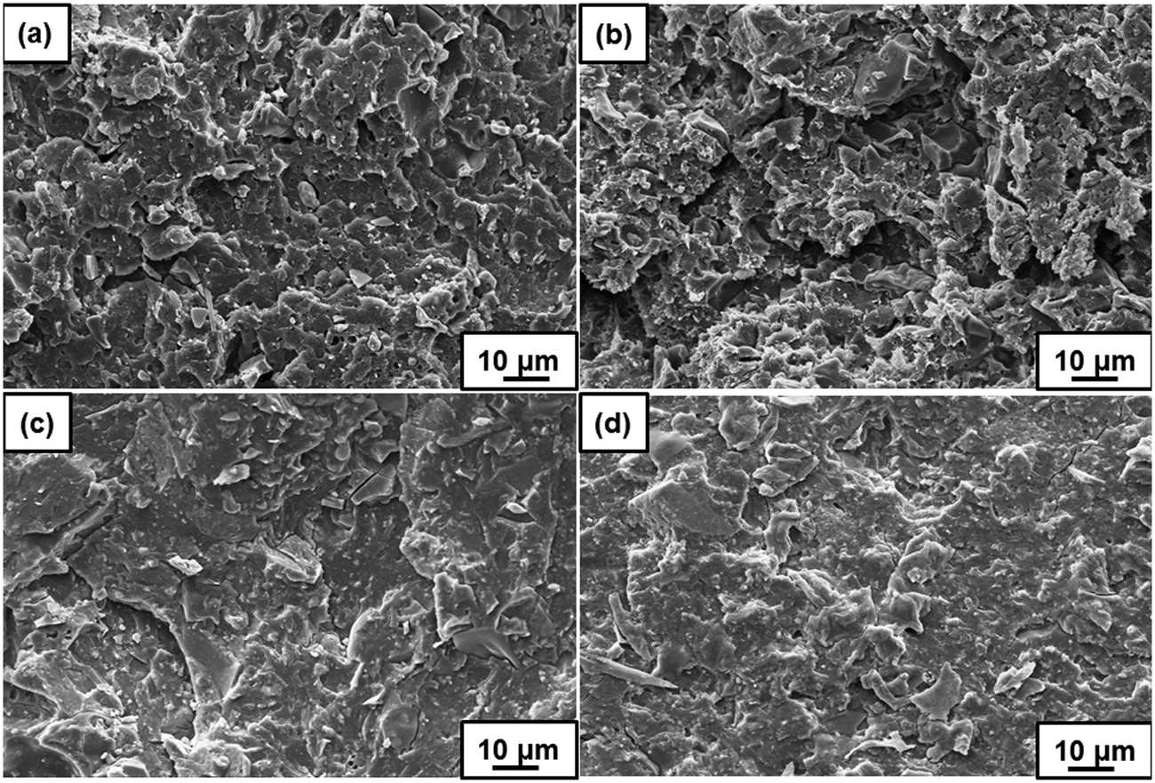 | ||
| Fig. 4 SEM micrographs of (a) NFO5, (b) NFO10, (c) NFO15 and (d) NFO20. | ||
The above referred chemico-physical properties have a strong influence on the MD coupling of composites. As the composite contains magnetic filler evenly dispersed in a dielectric matrix, there will be variation in relative permittivity under the application of an external magnetic field. Variation of relative permittivity as a function of frequency without the application of a magnetic field is shown in Fig. 5(a).
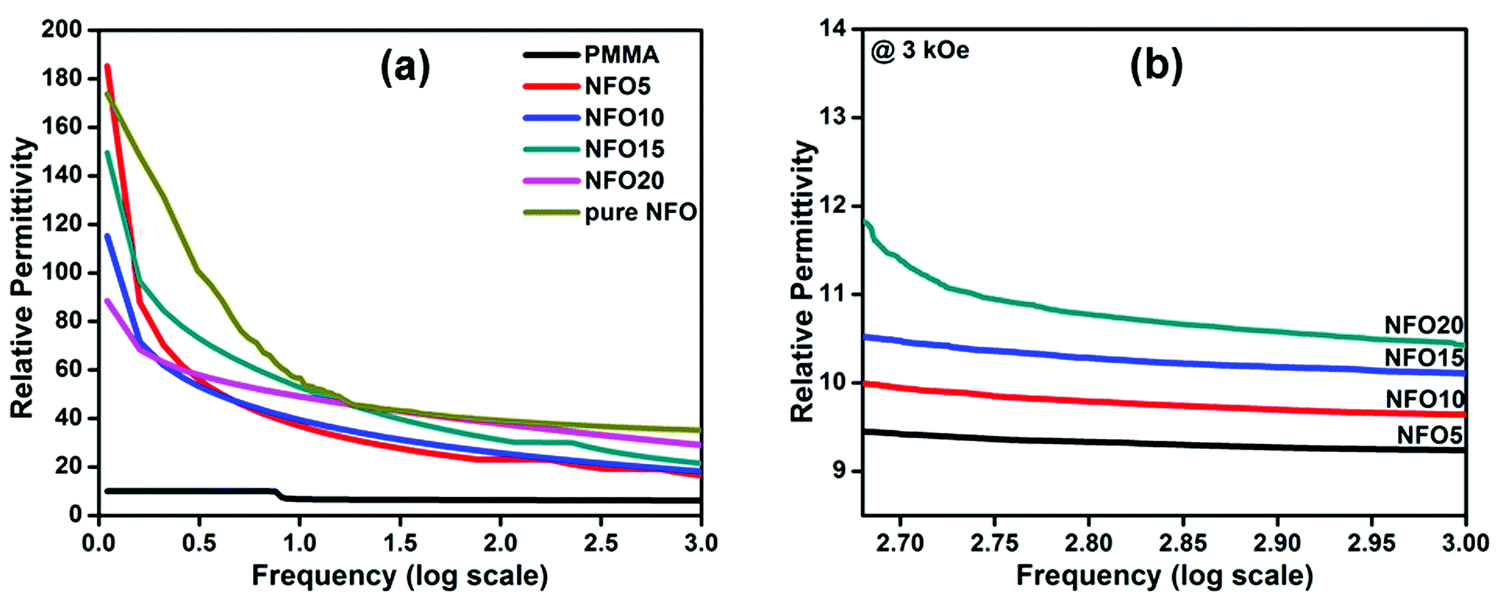 | ||
| Fig. 5 (a) Variation in the relative permittivity of the developed samples with respect to log frequency. (b) Variation in the relative permittivity of developed PMMA–NFO composites under the application of a 3 kOe magnetic field. | ||
From the figure, it is clear that relative permittivity decreases with an increase in log frequency. Usually in the low frequency region, the net polarization will be contributed by interfacial, dipolar, ionic and electronic polarizations, with interfacial polarization being the dominant one. But when the frequency increases, the contribution from different polarization mechanisms separates out. Due to this, net polarization will decrease as a function of frequency which in turn decreases the relative permittivity of the material. The values of relative permittivity measured at 1 MHz are given in Table 1.
| Composition | Relative permittivity at 1 MHz | –MC (%) at 1 MHz | |
|---|---|---|---|
| Without field | With a 3 kOe field | ||
| PMMA | 6.0 | — | — |
| NFO5 | 16.5 | 9.2 | 44.2 |
| NFO10 | 18.1 | 9.6 | 46.7 |
| NFO15 | 21.4 | 10.1 | 52.8 |
| NFO20 | 28.0 | 10.4 | 62.7 |
| NFO | 35.0 | — | — |
For normal intrinsic dielectrics, the dielectric properties are unaltered even if a magnetic field is applied, whereas for MDs, they are. Look at the variation in dielectric permittivity with the application of a 3 kOe magnetic field, as shown in Fig. 5(b). Here, one can observe a decrease in the values of relative permittivity for all the composites developed when a magnetic field of 3 kOe is applied. This confirms the existence of magnetocapacitance in the developed composites, which can occur due to several reasons such as chemical inhomogeneity and electrical heterogeneity.
The coupling between magnetic and electric polarization is to be understood more profoundly, which is usually estimated qualitatively by measuring the variation in relative permittivity under the application of an external magnetic field. This change in relative permittivity with a magnetic field is termed MD coupling and is defined as in eqn (1).
 | (1) |
PMMA is a known diamagnetic material, and hence it will not show any variation in relative permittivity when a magnetic field is applied. Here, all composites show a variation in relative permittivity when a magnetic field is applied, as summarized in Table 1. As shown, the samples show a decrease in relative permittivity under a magnetic field and hence result in a negative value for magnetocapacitance. It should be noted that the composite samples exhibit a high level of MC, hinting towards strong MD coupling in these materials, which is due to the magnetostrictive strain produced by spinel ferrite, NFO. This strain in turn induces variations in the dipolar order within the polymer, giving rise to different dipolar mobility when a magnetic field is applied.20 Thus the permittivity of the NFO-PMMA system decreases with the application of a strong magnetic field.
In the case of non-ferroelectric MD systems, usually the second derivative of Ginzburg–Landau free energy is taken with respect to polarization and is proportional to M2, where M is the magnetization.56,57 It is clear that the magnetization value increases with an increase in filler loading, as per Table S1 (ESI†). Hence, MD coupling increases as the volume fraction of NFO is increased from 0.05 to 0.2 in the PMMA matrix which is reflected in the MC measurements.
Fig. 6(a) represents the variation of magnetocapacitance as a function of applied magnetic field. Here, magnetocapacitance shows a variation as the magnetic field is increased. The MC behaviour in the composites could be explained using the effect of a magnetic field on the properties of charge separation structures.58 The magnetic field will decrease the magnetic as well as charge ordering in the magnetic phase of the composite and as a result the MC value will change.59 Hence, an increase in the magnetic field will lead to the enhanced negative magnetocapacitance value in the composite at room temperature. However, no signature of the existence of an electromechanical resonance frequency is visible anywhere in the frequency range we examined.
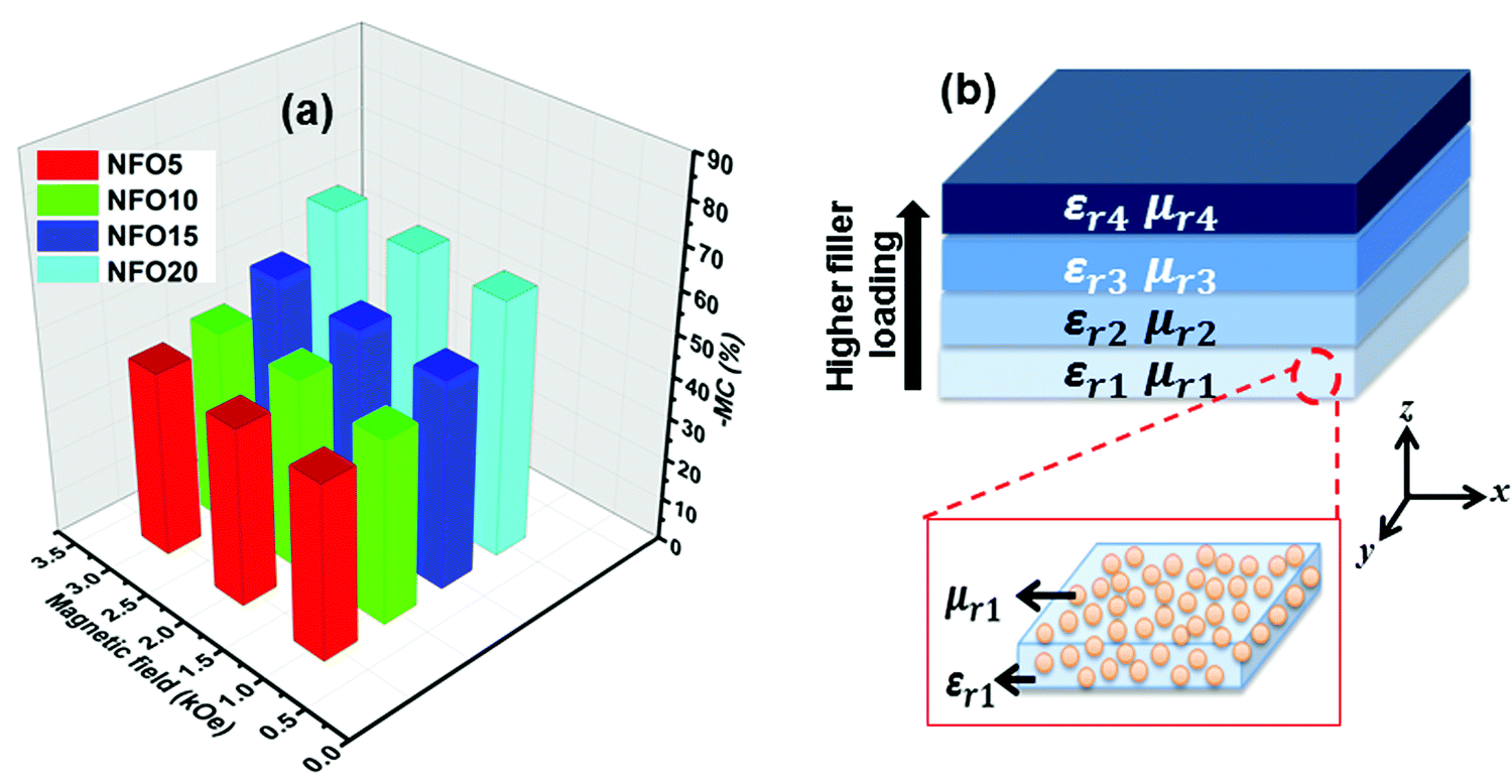 | ||
| Fig. 6 (a) Variation in magnetocapacitance with the application of different magnetic fields in the PMMA–NFO composites. (b) A schematic showing the developed functionally graded MD substrate and the enlarged single layer of the composite that contains magnetic filler in the PMMA matrix. | ||
As the MD properties show promising results, they can be further used for the benefit of antenna miniaturization. Our idea is to explore whether the developed composites can be used as substrates for antenna miniaturization, as they have agreeing values for both relative permittivity and magnetic permeability which will in turn reduce the resonant wavelength of half wave patch antennas and hence miniaturize them. To achieve this, the dielectric and magnetic properties of the material have to be tuned carefully without compromising the low loss behaviour. Tailoring the properties of such a single layer MD substrate is inappropriate for a wide spectrum of operational frequencies and the size reduction also quenches the bandwidth, S11, and directivity of the antennas compared with a dielectric substrate due to field confinement.60 Graded composites have recently evolved as a solution to this problem and they can effectively improve the antenna characteristics.61 Additional miniaturization is also reported for uniaxially graded composites as the top-down reduction in functionality imparts a blue shift in the resonant wavelength.62
Hence we developed a functionally graded anisotropic substrate in which the properties such as εr and μr vary in the z plane (Fig. 6(b)), through a polymer hot pressing technique. This can be conveniently realized by stacking all four developed composites together with each layer consisting of NFO fillers embedded in the PMMA matrix, but with different filler loading. The composite with a minimum filler loading is kept near the ground plane and then the rest are arranged with increasing filler loading to the patch, so as to yield a functionally graded substrate as shown in Fig. 6(b).
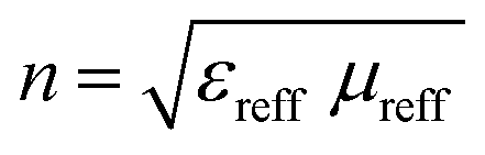
For understanding the values of εr and μr in composites with different volume fractions of NFO (0.05 Vf, 0.1 Vf, 0.15 Vf, 0.2 Vf), waveguide measurements in the X band using the Nicolson–Ross–Weir method63 were obtained, which are shown in Fig. 7.
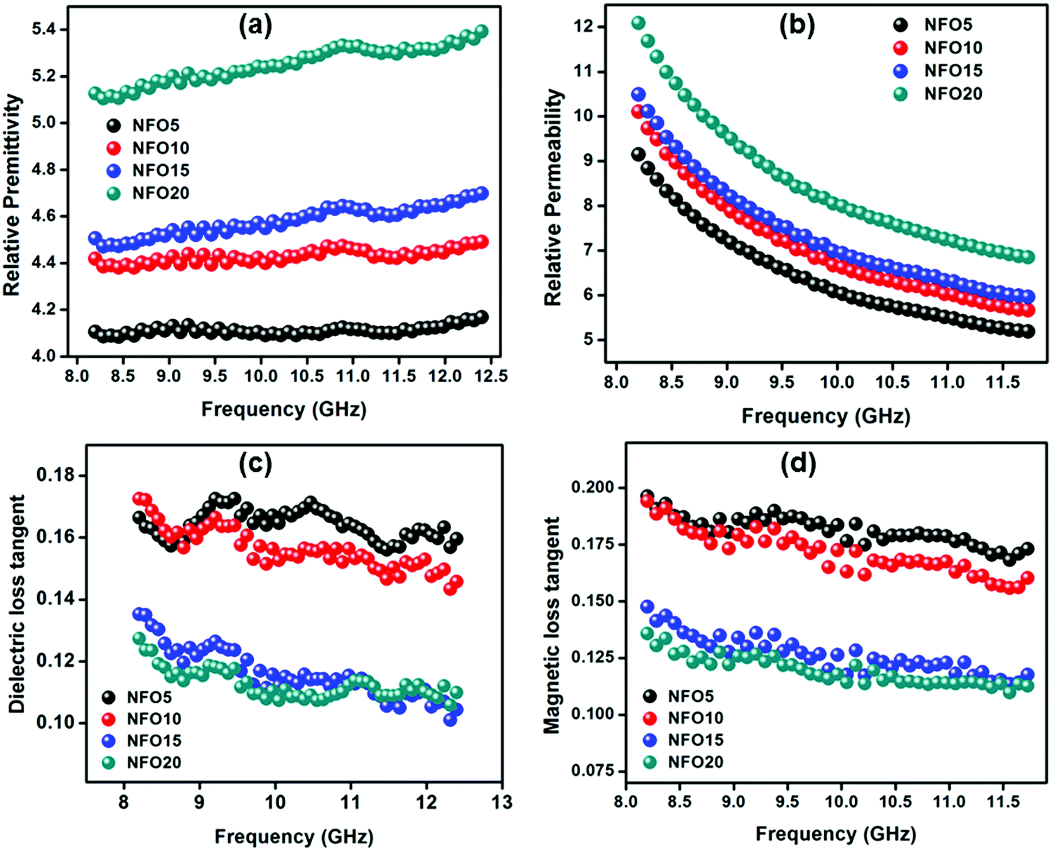 | ||
| Fig. 7 Variation in (a) relative permittivity, (b) relative permeability, (c) dielectric loss tangent and (d) magnetic loss tangent with respect to frequency in the X band. | ||
The variation in the real part of relative permittivity and relative permeability with respect to frequency is shown in Fig. 7(a) and (b) respectively. The real part in the dielectric and magnetic property is attributed to the ability of dipoles and spins to store electric and magnetic energy, respectively.64 The relative permittivity of the composite increases with an increase in filler content which is obviously due to the incorporation of a higher amount of NFO with a higher relative permittivity (due to the higher polarizability), than the PMMA matrix. Marginal variation is seen for the values of relative permittivity with respect to frequency. In the case of relative permeability, the value increases with an increase in filler content and is obviously due to the higher amount of magnetic component in the composite. The dielectric loss tangent and magnetic loss tangent are shown in Fig. 7(c) and (d) respectively. The ratio of the imaginary to the real part of relative permittivity and relative permeability are given by dielectric (tanδe = ε′′/ε′) as well as magnetic loss tangents (tanδm = μ′′/μ′). The loss values are in the order of 10−1 for all composites and show a marginal dispersion which is only within the error limits of the waveguide measurement setup. The applicability of the developed functionally graded composite as an antenna substrate is challenging here, due to its slightly lossy dielectric behavior. Instead, this developed composite can be used as the load in a low loss substrate, beneath the patch, so as to reduce the antenna dimensions effectively without compromising the antenna performance.65,66 One has to carefully choose the geometry of such a loading, as it is reported to control the characteristics of the radiation pattern.
In order to validate the usefulness of the developed laminar MD composites for size reduction in antennas, a model assisted study on the fabrication of a microstrip patch antenna (MPA) is carried out. Simply put, microstrip patch antennas are a class of planar antennas, consisting of a regular shaped metal patch etched out on a dielectric substrate which is excited using a voltage source across the microstrip patch and the conductive ground plane. The microstrip antenna radiates due to the fringing fields around the antenna which is the maximum in the broadside direction (θ = 0), with no radiation along the edges of the substrate (θ = 90°), ideally. Our idea is to replace the isotropic dielectric substrate with a magnetodielectric substrate with engineered axial anisotropy. Usually, the antennas equipped with high permittivity substrates have inferior bandwidths. A tricky way to increase the bandwidth several times is to introduce a z-axial anisotropic substrate while maintaining in-plane isotropy.67 This design, although novel, is an engineering hazard, which is successfully demonstrated in the present work.
Initially, different laminar substrates are modelled in ANSYS HFSS using the following concepts; (i) a lossless dielectric substrate (LD) (εr = μr = 1), (ii) a low loss Arlon substrate loaded with ungraded magneto dielectric material (UMD) (εr = 4.65; μr = 6.60) and (iii) finally, a low loss Arlon substrate loaded with uniaxially graded magneto dielectric material (GMD). In both the latter cases, the Arlon low loss substrate is loaded with the MD materials beneath the patch, to minimize the losses arising from the material properties. The UMD substrate is loaded with the functionally graded MG composite treated as a whole, without considering the uniaxial variation in the properties. On the other hand, the GMD substrate is modelled with the uniaxial variation in magnetic and dielectric properties. Microstrip patch antennas (MPA) operating at 830 MHz using these MD loaded substrates are theoretically modelled, simulated, and optimized using ANSYS HFSS. Geometrical optimization was carried out on the theoretical design of the GMD substrate MPA to improve the antenna characteristics, including the return loss, gain, and bandwidth. During the optimization process, parametric studies on the effect of substrate dimensions were carried out to attain optimal performance, by keeping the dimensions of the patch and the GMD substrate constant. Loading the low loss substrate with the GMD material altered the resonant frequency and the performance characteristics of the theoretical model, which was systematically brought to the designed operating frequency by the optimization process. Fig. 8 is a schematic representation of MPA employing a GMD substrate and the uniaxial variation in magnetic and dielectric properties. The antenna parameters and geometry of the optimized design are compared with those of LD-MPA and UMD-loaded MPA to analyze the effect of employing MD loading for fabricating MPAs.
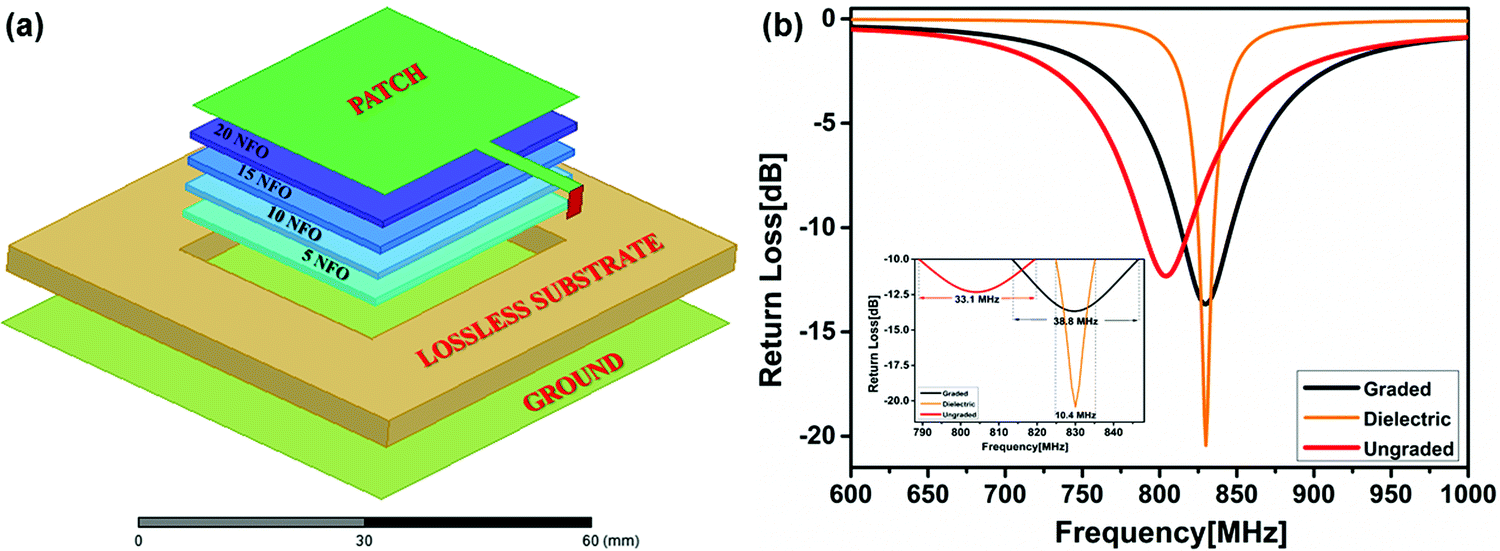 | ||
| Fig. 8 (a) A schematic showing MPA employing the GMD substrate and the uniaxial variation in MD properties. (b) Return loss characteristics of MPAs with LD substrate, and GMD and UMD substrates. (b inset) Bandwidth comparison of MPAs with the LD substrate, and GMD and UMD substrates. | ||
The efficiency of magnetodielectric loading in size reduction can be analyzed by a comparison of the geometric parameters of the optimized designs of LD, UMD, and GMD substrate MPAs. The geometric dimensions of the optimized designs are listed in Table 2.
| Dimension | LD substrate | UMD substrate | GMD substrate |
|---|---|---|---|
| Patch width (Wp) (mm) | 180.7 | 41 | 41 |
| Patch length (Lp) (mm) | 167.5 | 33.5 | 33.5 |
| Substrate width (Ws) (mm) | 362.5 | 73.6 | 73.6 |
| Substrate length (Ls) (mm) | 368.2 | 66.1 | 66.1 |
| Substrate height (h) (mm) | 4 | 4 | 4 |
| Area of patch (mm2) | 30267.2 | 1373.5 | 1373.5 |
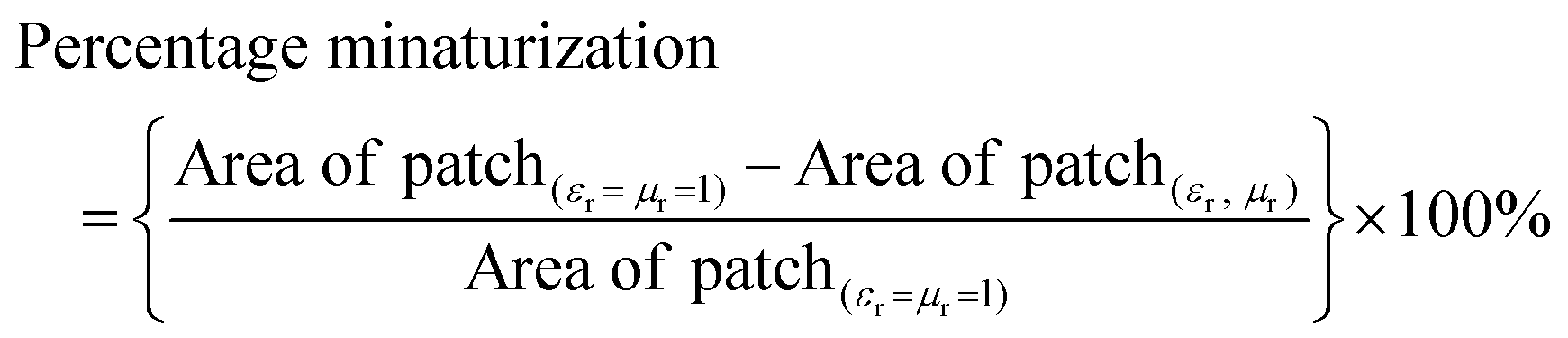
To identify the impact of the developed substrates in the field of antenna size miniaturization, one has to estimate the miniaturization factor given by the expression,
 | (2) |
 | (3) |
Interestingly, for the current MD antenna loaded with GMD and UMD substrates, an impressive miniaturization of 95.46% was observed when compared to an LD substrate. This result clearly justifies the introduction of an MD substrate in the patch antenna for a high degree of miniaturization. This is because magneto dielectric materials reduce the high field confinement of ordinary dielectric substrates and thereby reduce their capacitive behaviour, which in turn reduces the antenna dimensions.6 For practical realization, antenna parameters including return loss, bandwidth, gain, directivity, radiation efficiency, front to back ratio etc. have to be studied systematically.
To understand the acceptance of radio waves by the optimized MPA models, return loss characteristics were simulated in ANSYS HFSS and are shown in Fig. 8(b). The return loss characterization of an antenna describes the ratio of reflected and incident voltage wave amplitudes received by the antenna.68 The return loss of an LD substrate antenna was found to be 20.44 dB at 830 MHz, that of an UMD substrate antenna was 11.96 dB at 807 MHz and that of a GMD substrate antenna was 13.67 dB at 830 MHz. As shown, the return loss of MD loaded substrates is considerably decreased which can be attributed to the lossy nature of MD loading.69 Also a shift in the radiating frequency is observed for the UMD substrate loaded MPA. The UMD substrate antenna was simulated with the geometric parameters of the optimized GMD substrate antenna to understand the effects of including uniaxial grading of the MD properties in the model and hence causing the shift in radiating frequency. However, the return loss characteristics indicate that more than 90% of the incident radio wave is accepted by all three designs, which makes the MD loaded substrates suitable for practical applications.
An impendence bandwidth depicts the frequency range in which the antenna will have good impedance matching.70 A comparison of the bandwidth of three models is depicted in the inset of Fig. 8(b). Clearly, all three chosen models have significant impedance bandwidths. LD substrate antenna exhibit a bandwidth of only 10.4 MHz, which is found to be 33.1 MHz for UMD and 38.8 MHz for GMD substrates. A massive 237% increase in impedance bandwidth is observed for the GMD substrate antenna with respect to the LD substrate antenna. Such a whopping increase in bandwidth without using any high K materials has not been reported in the literature before. In the meantime, a reduction in impedance mismatch between the antenna substrate and the medium (air) is also observed which might have enhanced the bandwidth of MD loaded MPAs.6,65,71 In this way, significant improvement in the bandwidth of MPA is achieved using MD loaded axially anisotropic substrates, without compromising other parameters.
The spatial distribution of the strength of radio waves and the antenna gain of modeled antennas is simulated using ANSYS HFSS and is depicted in Fig. 9. Spatial distribution of the radiated waves is the radiation pattern.72 The radiation pattern of lossless dielectric depicts a nearly spherical distribution of radiated power with a peak perpendicular to the surface of the patch (Fig. 9(a)). The radiated peak has a directivity of 8.96 while maintaining a front to back ratio of 231.3. Fig. 9(c) depicts the distribution of the antenna gain and the peak gain was observed to be 9.16, indicating a highly directional beam of radiated power emitted perpendicular to the antenna surface with a negligible back lobe and excellent power conversion by the modelled antenna.
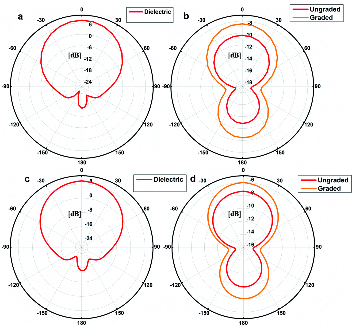 | ||
| Fig. 9 Radiation pattern of (a) LD substrate, and (b) GMD and UGD substrate; gain plots of (c) LD substrate, and (d) GMD and UMD substrate. | ||
The radiation pattern of the UMD and GMD substrate antenna is depicted in Fig. 9(b). It can be observed that the distribution of the radio waves is diminished, indicating the dissipation of radio waves within the substrate. However, the radiated pattern had a directivity of 1.97 and 2.18 for GMD and UMD respectively. Also peak gains of 0.24 and 0.16 were observed for the GMD and UMD substrate antennas respectively, which are however low for practical applications. The front to back ratio was observed to be considerably lower as 1.66 for GMD and 1.82 for UMD indicating confinement of the radiated power with the substrate as can be observed from Fig. 9(d) depicting the back lobes in the radiation pattern. The real time testing of the antenna parameters will be attempted in subsequent research and will be published elsewhere.
In next generation communication devices aiming for huge antenna miniaturization, the figures obtained in the present study are significant. Hence we can conclude that the newly developed MD functionally graded composite with PMMA–NiFe2O4 is a potential candidate in antenna miniaturization and bandwidth enhancement. However, the radiation characteristics of the modelled antennas have to be improved which is due to the high loss tangent of ferrite incorporated PMMA composites. The impedance characteristics show appropriate impedance matching but the input power is dissipated by the lossy nature of MD loading and hence reducing the return loss, gain and radiation efficiency of the modelled antennas. Improvement in the material properties i.e. reduction in the dielectric and magnetic loss of the MD loading will improve the antenna parameters. Furthermore, the simulation results clearly indicate that treatment of the uniaxial anisotropy has to be considered separately while modelling, so that the antenna parameters can be evaluated more precisely rather than treating the composite as a whole.
Conclusions
Microstrip patch antennas are thin planar antennas that can be easily realized on printed circuit boards, consumer electronic products, aircrafts and missiles. There have been continuous efforts to miniaturize patch antennas using high permittivity material substrates, introducing defects in the metallic ground plane, reshaping the radiating element, use of metamaterials etc. The latest in this list is the introduction of magnetodielectric (MD) substrates. In comparison to dielectric only substrates, employing MD substrates for antenna miniaturization offer many advantages in addition to impedance matching and reduced capacitive coupling. In the present study, polymer composites consisting of NiFe2O4 as the magnetic phase and PMMA as the dielectric phase were used to fabricate the MD substrate. NFO was synthesized via a polymer pyrolysis method. The structural as well as the magnetic studies were performed for the developed NFO. Composites based on PMMA and NFO were synthesized using a solution blending technique, using DMF as the solvent. The structural, microstructural and magnetic characterizations were performed over various volume fractions of NFO loaded samples (0.05 Vf, 0.1 Vf, 0.15 Vf and 0.2 Vf). The MD measurements showed that the maximum filler loaded sample has an impressive magnetocapacitance value of −62.7%. A functionally graded anisotropic composite was made by systematically stacking the different filler loaded samples, with laminates having more solid loading at the top layer. The rationale is that such a design can bring about a blue shift in the resonant wavelength, in addition to the bandwidth enhancement.The proposed antenna was theoretically designed to operate at 830 MHz using the properties of the developed anisotropic composite as the loading in the substrate. It was observed that a whopping 95.46% size reduction can be attained using the present functionally graded composite when compared to a substrate material with εr = μr = 1. However, the lossy nature of the ferrite incorporated PMMA composites diminished the radiation characteristics of modelled antennas, which can be improved by appropriate design of the individual laminar composites. Notwithstanding this, the proposed strategy of introducing functionally gradient and axially anisotropic substrates to patch antennas, is ideal for large scale antenna miniaturization, in addition to bandwidth enhancement.
Conflicts of interest
There are no conflicts to declare.Acknowledgements
The author D. R. Lekshmi thanks the University Grants Commission, New Delhi for the financial support. The author K. P. Surendran acknowledge Council of Scientific and Industrial Research, New Delhi, for funding through a Niche Creating Project (MLP 0044) and Indian Space Research Organization, Bengaluru for financial support through a Respond Project (No. ISRO/RES/3/884/21-22). The authors are also thankful to Mr Harish Raj for SEM, Dr Subrata Das for XRD measurements, Mr Kiran Mohan for TEM, and Dr Manoj R. Varma for PPMS measurements.References
- W. Eerenstein, N. D. Mathur and J. F. Scott, Nature, 2006, 442, 759–765 CrossRef CAS PubMed.
- J. F. Scott, Nat. Mater., 2007, 6, 256–257 CrossRef CAS PubMed.
- N. Altunyurt, M. Swaminathan, P. M. Raj and V. Nair, Proc. – Electron. Components Technol. Conf., 2009, 801–808 CAS.
- I. A. Abdel-Latif, Multiferroics Materials, Future of Spintronics, Materials Research Foundations, 2019, vol. 57, pp. 89–112, DOI: 10.21741/9781644900390–5 Search PubMed.
- P. Anithakumari, B. P. Mandal, E. Abdelhamid, R. Naik and A. K. Tyagi, RSC Adv., 2016, 6, 16073–16080 RSC.
- H. Mosallaei and K. Sarabandi, IEEE Trans. Antennas Propag., 2004, 52, 1558–1567 CrossRef.
- N. Hur, S. Park, P. A. Sharma, S. Guha and S. Cheong, Phys. Rev. Lett., 2004, 93, 3–6 CrossRef PubMed.
- V. J. Folen, G. T. Rado and E. W. Stalder, Phys. Rev. Lett., 1961, 6, 607–608 CrossRef CAS.
- Z. Huang, Y. Cao, Y. Sun, Y. Xue and C. Chu, Phys. Rev. B: Condens. Matter Mater. Phys., 1997, 56, 2623–2626 CrossRef CAS.
- Y. Tokunaga, N. Furukawa, H. Sakai, Y. Taguchi, T. H. Arima and Y. Tokura, Nat. Mater., 2009, 8, 558–562 CrossRef CAS PubMed.
- N. A. Algarou, Y. Slimani, M. A. Almessiere, F. S. Alahmari, M. G. Vakhitov, D. S. Klygach, S. V. Trukhanov, A. V. Trukhanov and A. Baykal, J. Mater. Res. Technol., 2020, 9, 5858–5870 CrossRef CAS.
- M. A. Almessiere, S. Güner, Y. Slimani, M. Hassan, A. Baykal, M. A. Gondal, U. Baig, S. V. Trukhanov and A. V. Trukhanov, Nanomaterials, 2021, 11, 2461 CrossRef CAS PubMed.
- M. A. Subramanian, T. He, J. Chen, N. S. Rogado, T. G. Calvarese and A. W. Sleight, Adv. Mater., 2006, 18, 1737–1739 CrossRef CAS.
- I. V. Lisnevskaya, I. A. Bobrova, T. G. Lupeiko, M. R. Agamirzoeva and K. V. Myagkaya, J. Magn. Magn. Mater., 2016, 405, 62–65 CrossRef CAS.
- Y. Wu, J. Li, Z. Q. Zhang and C. T. Chan, Phys. Rev. B: Condens. Matter Mater. Phys., 2006, 74, 1–9 Search PubMed.
- M. Naveed Ul-Haq, T. Yunus, A. Mumtaz, V. V. Shvartsman and D. C. Lupascu, J. Alloys Compd., 2015, 640, 462–467 CrossRef CAS.
- Y. P. Yao, Y. Hou, S. N. Dong and X. G. Li, J. Appl. Phys., 2011, 110, 014508 CrossRef.
- Y. Han, L. Li, D. Guo, X. Ren and W. Xia, Mater. Lett., 2013, 98, 19–21 CrossRef CAS.
- P. Martins and S. Lanceros-Méndez, Adv. Funct. Mater., 2013, 23, 3371–3385 CrossRef CAS.
- P. Martins, D. Silva, M. P. Silva and S. Lanceros-Mendez, Appl. Phys. Lett., 2016, 109, 1–20 CrossRef.
- S.-E. Lee, S. P. Choi, K.-S. Oh, J. Kim, S. M. Lee and K. R. Cho, Materials, 2020, 13, 1021 CrossRef CAS PubMed.
- S. Aggarwal, K. S. Sreeja, S. Chakrabarti, V. R. Palkar and A. R. Bhattacharyya, RSC Adv., 2016, 6, 42892–42898 RSC.
- S. E. Lee, H. J. Kim, J. H. Lee, K. S. Oh, H. T. Hahn and J. W. Choi, Mater. Lett., 2017, 187, 94–97 CrossRef CAS.
- M. A. Darwish, A. V. Trukhanov, O. S. Senatov, A. T. Morchenko, S. A. Saafan, K. A. Astapovich, S. V. Trukhanov, E. L. Trukhanova, A. A. Pilyushkin, A. S. B. Sombra, D. Zhou, R. B. Jotania and C. Singh, Nanomaterials, 2020, 10, 492 CrossRef CAS PubMed.
- O. Yakovenko, O. Lazarenko, L. Matzui, L. Vovchenko, M. Borovoy, P. Tesel’ko, O. Lozitsky, K. Astapovich, A. Trukhanov and S. Trukhanov, J. Mater. Sci., 2020, 55, 9385–9395 CrossRef CAS.
- S. Ramesh and L. C. Wen, Ionics, 2010, 16, 255–262 CrossRef CAS.
- M. M. Demir, K. Koynov, Ü. Akbey, C. Bubeck, I. Park, I. Lieberwirth and G. Wegner, Macromolecules, 2007, 40, 1089–1100 CrossRef CAS.
- G. M. Nasr, E. Mousa and M. M. Haroun, Egypt. J. Pet., 2019, 28, 361–369 CrossRef.
- P. Maji and R. B. Choudhary, Mater. Chem. Phys., 2017, 193, 391–400 CrossRef CAS.
- D. A. Vinnik, V. E. Zhivulin, D. P. Sherstyuk, A. Y. Starikov, P. A. Zezyulina, S. A. Gudkova, D. A. Zherebtsov, K. N. Rozanov, S. V. Trukhanov, K. A. Astapovich, A. S. B. Sombra, D. Zhou, R. B. Jotania, C. Singh and A. V. Trukhanov, J. Mater. Chem. C, 2021, 9, 5425–5436 RSC.
- D. A. Vinnik, V. E. Zhivulin, D. P. Sherstyuk, A. Y. Starikov, P. A. Zezyulina, S. A. Gudkova, D. A. Zherebtsov, K. N. Rozanov, S. V. Trukhanov, K. A. Astapovich, V. A. Turchenko, A. S. B. Sombra, D. Zhou, R. B. Jotania, C. Singh and A. V. Trukhanov, Mater. Today Chem., 2021, 20, 100460 CrossRef CAS.
- D. I. Tishkevich, I. V. Korolkov, A. L. Kozlovskiy, M. Anisovich, D. A. Vinnik, A. E. Ermekova, A. I. Vorobjova, E. E. Shumskaya, T. I. Zubar, S. V. Trukhanov, M. V. Zdorovets and A. V. Trukhanov, J. Alloys Compd., 2019, 797, 573–581 CrossRef CAS.
- M. A. Almessiere, A. V. Trukhanov, F. A. Khan, Y. Slimani, N. Tashkandi, V. A. Turchenko, T. I. Zubar, D. I. Tishkevich, S. V. Trukhanov, L. V. Panina and A. Baykal, Ceram. Int., 2020, 46, 7346–7354 CrossRef CAS.
- S. V. Trukhanov, A. V. Trukhanov, V. G. Kostishin, L. V. Panina, I. S. Kazakevich, V. A. Turchenko, V. V. Oleinik, E. S. Yakovenko and L. Y. Matsui, J. Exp. Theor. Phys., 2016, 123, 461–469 CrossRef CAS.
- M. V. Zdorovets, A. L. Kozlovskiy, D. I. Shlimas and D. B. Borgekov, J. Mater. Sci.: Mater. Electron., 2021, 32, 16694–16705 CrossRef CAS.
- J. Wang, F. Ren, R. Yi, A. Yan, G. Qiu and X. Liu, J. Alloys Compd., 2009, 479, 791–796 CrossRef CAS.
- A. Thakur, N. Sharma, M. Bhatti, M. Sharma, A. V. Trukhanov, S. V. Trukhanov, L. V. Panina, K. A. Astapovich and P. Thakur, Nano-Structures Nano-Objects, 2020, 24, 100599 CrossRef CAS.
- D. I. Shlimas, A. L. Kozlovskiy and M. V. Zdorovets, J. Mater. Sci.: Mater. Electron., 2021, 32, 7410–7422 CrossRef CAS.
- X. Liu, G. Yang and S. Fu, Mater. Sci. Eng., C, 2007, 27, 750–755 CrossRef CAS.
- M. M. Hessien, N. Y. Mostafa and O. H. Abd-Elkader, J. Magn. Magn. Mater., 2016, 398, 109–115 CrossRef CAS.
- Z. Zhang, Y. Liu, G. Yao, G. Zu, D. Wu and Y. Hao, Ceram. Int., 2012, 38, 3343–3350 CrossRef CAS.
- S. V. Trukhanov, V. A. Khomchenko, L. S. Lobanovski, M. V. Bushinsky, D. V. Karpinsky, V. V. Fedotova, I. O. Troyanchuk, A. V. Trukhanov, S. G. Stepin, R. Szymczak, C. E. Botez and A. Adair, J. Exp. Theor. Phys., 2006, 103, 398–410 CrossRef CAS.
- A. L. Kozlovskiy and M. V. Zdorovets, Mater. Chem. Phys., 2021, 263, 124444 CrossRef CAS.
- G. Nabiyouni, M. J. Fesharaki, M. Mozafari and J. Amighian, Chinese Phys. Lett., 2010, 27, 126401 CrossRef.
- N. Yang, C. Xu, J. Hou, Y. Yao, Q. Zhang, M. E. Grami, L. He, N. Wang and X. Qu, RSC Adv., 2016, 6, 18279–18287 RSC.
- T. Bel, N. Yahya, H. Cimenoglu, C. Arslan and N. Baydogan, J. Phys. Conf. Ser., 2018, 1123, 012005 CrossRef.
- S. Atta, M. Haldar, A. K. Das and A. K. Meikap, Phys. E, 2019, 114, 113632 CrossRef CAS.
- M. S. Tamboli, P. K. Palei, S. S. Patil, M. V. Kulkarni, N. N. Maldar and B. B. Kale, Dalton Trans., 2014, 43, 13232–13241 RSC.
- F. Wang, Y. Yao, X. Zeng, T. Huang, R. Sun, J. Xu and C. P. Wong, RSC Adv., 2016, 6, 41630–41636 RSC.
- A. T. Nelson, J. T. White, D. A. Andersson, J. A. Aguiar, K. J. McClellan, D. D. Byler, M. P. Short and C. R. Stanek, J. Am. Ceram. Soc., 2014, 97, 1559–1565 CrossRef CAS.
- C. W. Nan, R. Birringer, D. R. Clarke and H. Gleiter, J. Appl. Phys., 1997, 81, 6692–6699 CrossRef CAS.
- M. T. Sebastian and H. Jantunen, Int. J. Appl. Ceram. Technol., 2010, 7, 415–434 CAS.
- L. Holliday and J. Robinson, J. Mater. Sci., 1973, 8, 301–311 CrossRef CAS.
- I. Troyanchuk, S. Trukhanov, D. Khalyavin and H. Szymczak, J. Magn. Magn. Mater., 2000, 208, 217–220 CrossRef CAS.
- A. Kozlovskiy, K. Egizbek, M. V. Zdorovets, M. Ibragimova, A. Shumskaya, A. A. Rogachev, Z. V. Ignatovich and K. Kadyrzhanov, Sensors, 2020, 20, 4851 CrossRef CAS PubMed.
- G. Lawes, A. P. Ramirez, C. M. Varma and M. A. Subramanian, Phys. Rev. Lett., 2003, 91, 1–4 CrossRef PubMed.
- G. Lawes, T. Kimura, C. M. Varma, M. A. Subramanian, N. Rogado, R. J. Cava and A. P. Ramirez, Prog. Solid State Chem., 2009, 37, 40–54 CrossRef CAS.
- R. F. Mamin, T. Egami, Z. Marton and S. A. Migachev, Ferroelectrics, 2007, 348, 7–12 CrossRef CAS.
- S. Arumugam, P. Sivaprakash, A. Dixit, R. Chaurasiya, L. Govindaraj, M. Sathiskumar, S. Chatterjee and R. Suryanarayanan, Sci. Rep., 2019, 9, 1–8 Search PubMed.
- P. Ikonen, K. N. Rozanov, A. V. Osipov and S. A. Tretyakov, IEEE Trans. Antennas Propag., 2006, 54, 3391–3399 Search PubMed.
- D. Sarmah, N. Bhattacharyya and S. Bhattacharyya, IEEE Trans. Dielectr. Electr. Insul., 2013, 20, 1845–1850 CAS.
- F. Bouttout, F. Benabdelaziz, A. Benghalia, D. Khedrouche and T. Fortaki, Electron. Lett., 1999, 35, 255–256 CrossRef.
- C. Larsson, D. Sjöberg and L. Elmkvist, Tech. Rep. LUTEDX/(TEAT-7196).
- A. Arora and S. Bindra, Appl. Phys. A: Mater. Sci. Process., 2017, 123, 0–5 CrossRef CAS.
- R. C. Hansen and M. Burke, Microw. Opt. Technol. Lett., 2000, 26, 75–78 CrossRef.
- P. M. T. Ikonen, S. I. Maslovski, C. R. Simovski and S. A. Tretyakov, IEEE Trans. Antennas Propag., 2006, 54, 1654–1662 CrossRef.
- Ç. S. Gürel and E. Yazgan, IEEE Trans. Antennas Propag., 2004, 52, 2532–2537 CrossRef.
- A. Elrashidi, K. Elleithy and H. Bajwa, Int. J. Networks Commun., 2012, 2, 13–19 CrossRef.
- S. S. Shukla, R. K. Verma and G. S. Gohir, 2015 4th Int. Conf. Reliab. Infocom Technol. Optim. Trends Futur. Dir. ICRITO 2015, 2015, pp. 1–3.
- B. D. Orban and G. J. K. Moernaut, The Basics of Patch Antennas, 2005 Search PubMed.
- H. Mosallaei and K. Sarabandi, IEEE Trans. Antennas Propag., 2004, 52, 2403–2414 CrossRef.
- Constantine A. Balanis, Antenna Theory: Analysis and Design, Wiley, 3rd edn, 2005 Search PubMed.
Footnote |
| † Electronic supplementary information (ESI) available: Fig. S1: (a) WAXD of pristine PMMA along with the developed composites. (b) TG profile of PMMA and the composites. See DOI: 10.1039/d1ma00844g |
| This journal is © The Royal Society of Chemistry 2022 |