
High throughput screening of novel tribromide perovskite materials for high-photovoltage solar cells†
Shi
Chen‡
 abc,
Lihua
Zhang‡
bd,
Yanliang
Liu‡
b,
Zhuoqiong
Zhang
e,
Yang
Li
b,
Weizheng
Cai
b,
Haiyan
Lv
b,
Yanchun
Qin
b,
Qianlong
Liao
b,
Bin
Zhou
b,
Ting
Yan
b,
Jie
Ren
b,
Shuming
Chen
f,
Xiaodong
Xiang
b,
Songyuan
Dai
g,
Shu Kong
So
e,
Xingzhu
Wang
*ab,
Shihe
Yang
*dh and
Baomin
Xu
*b
abc,
Lihua
Zhang‡
bd,
Yanliang
Liu‡
b,
Zhuoqiong
Zhang
e,
Yang
Li
b,
Weizheng
Cai
b,
Haiyan
Lv
b,
Yanchun
Qin
b,
Qianlong
Liao
b,
Bin
Zhou
b,
Ting
Yan
b,
Jie
Ren
b,
Shuming
Chen
f,
Xiaodong
Xiang
b,
Songyuan
Dai
g,
Shu Kong
So
e,
Xingzhu
Wang
*ab,
Shihe
Yang
*dh and
Baomin
Xu
*b
aAcademy for Advanced Interdisciplinary Studies, Southern University of Science and Technology, Shenzhen, Guangdong Province 518055, China. E-mail: wangxz@sustech.edu.cn
bDepartment of Materials Science and Engineering, Shenzhen Engineering Research and Development Center for Flexible Solar Cells, Southern University of Science and Technology, Shenzhen, Guangdong Province 518055, China. E-mail: xubm@sustech.edu.cn
cHenan Key Laboratory of Photovoltaic Materials, Henan University, Kaifeng 475004, China
dDepartment of Chemistry, The Hong Kong University of Science and Technology, Clear Water Bay, Kowloon, Hong Kong, China
eDepartment of Physics, Hong Kong Baptist University, Kowloon Tong, Hong Kong, China
fDepartment of Electrical and Electronic Engineering, Southern University of Science and Technology, Shenzhen, Guangdong Province 518055, China
gState Key Laboratory of Alternate Electrical Power System with Renewable Energy Sources, North China Electric Power University, Beijing 102206, China
hGuangdong Key Lab of Nano-Micro Material Research, School of Chemical Biology and Biotechnology, Shenzhen Graduate School, Peking University, Shenzhen, Guangdong Province 518055, China. E-mail: chsyang@pku.edu.cn
First published on 25th October 2021
Abstract
An efficient search for numerous novel mixed perovskite materials for high-performance solar cells leads to a strong demand for high throughput screening protocols. Highly efficient composition screening based on high throughput fabrication of discontinuous rather than compact perovskite films with comparable properties, which can save plenty of time and effort required for optimizing dense films and can significantly expand the applicability of the screening method to various perovskite compositions, has seldom been investigated. Especially, tribromide perovskites (∼2.3 eV bandgap) with promising applications in tandem and spectral splitting devices require the efficient screening of new constituents to yield a high open-circuit voltage (Voc). Herein, we develop a highly efficient composition screening protocol based on high throughput inkjet printing of discontinuous perovskite films with representative and comparable properties to accelerate the discovery of novel tribromide perovskites for high-photovoltage solar cells. 30 tribromide perovskite films with similar bandgaps are speedily and automatically inkjet-printed, and a very close grain size is acquired for all samples via optimizing the crystallization. Therefore, the corresponding photoluminescence (PL) lifetime database allows the efficient screening and identification of new constituents for high-photovoltage devices. To validate this, among the 30 samples, two compositions (HC(NH2)2)0.4(CH3NH3)0.6PbBr3 (FA0.4MA0.6) and (HC(NH2)2)0.1(CH3NH3)0.9PbBr3 (FA0.1MA0.9) with a long and short average PL lifetime, respectively, are screened out for device comparison. As expected, the FA0.4MA0.6 device delivers a high Voc of 1.60 V with a champion efficiency of 9.25%, which is among the highest reported Voc values for tribromide devices, much higher than that (1.45 V and 6.62%) of the FA0.1MA0.9 counterpart. Surprisingly, the Voc limit for both devices is determined to be as high as 2.01 V for the first time. The Voc and efficiency improvements principally result from the reduced trap states, lower level of energetic disorder, more efficient charge transport and decreased charge recombination losses. Additionally, the validity of the PL lifetime database is further confirmed by a high Voc of 1.55 V obtained for another novel composition. These findings open up a new avenue for accelerated discovery of new perovskites for advanced device applications.
1 Introduction
Hybrid organic–inorganic perovskites have been viewed as one of the most promising photovoltaic materials owing to their superior optoelectronic properties, and these materials are generally described with an ABX3 formula, where A denotes monovalent cations (such as CH3NH3+ (MA+), HC(NH2)2+ (FA+), and Cs+), B stands for divalent metal cations (namely Pb2+ and Sn2+), and X represents halide anions (i.e. I−, Br−, and Cl−).1–3 Currently, the utilization of lead-based perovskites with multiple cations and hybrid halides as active layers in perovskite solar cells is emerging as a particularly effective approach to further improve device efficiency and stability.4–8 Consequently, the combination of mixed multiple cations and hybrid halides generates a myriad of possible perovskite constituents. Such an enormous number of combinatorially available precursor compositions make the trial-and-error method time-consuming and inefficient, leading to a strong demand for high throughput synthesis. High throughput synthesis will permit the large-scale fabrication of perovskite films in a fast and reproducible manner, and the subsequent analysis regarding material properties will accelerate the discovery of novel perovskites for advanced device applications.In this aspect, several research groups tried to develop a high throughput technique suitable for perovskite synthesis.9–12 High throughput synthesis of perovskite single crystals and polycrystalline particles via a robot setup was demonstrated according to antisolvent crystallization.9,10 However, the above prepared perovskites existed in the form of particles rather than thin films, and thus the corresponding property comparison cannot afford an effective and direct forecast of film-based device performance. Furthermore, 75 unique perovskite-inspired films were fabricated and characterized using an accelerated platform within 2 months.11 This increased experimental throughput significantly accelerates the search for lead-free perovskites in the chemical space, but the preparation of dozens of perovskite films is still a major expenditure of time and the subsequent oversimplified property characterization (i.e. crystal phase and bandgap) cannot effectively identify the novel compositions for high-performance optoelectronic devices. Recently, our previous study developed a high throughput inkjet printing approach to fabricate 25 mixed perovskite films in 10 minutes, and the subsequently obtained bandgaps and PL lifetimes of these films allowed the accelerated screening of perovskite constituents for photovoltaic applications.12 Apparently, this type of composition screening based on high throughput inkjet printing is very useful for the discovery of novel perovskites, but the pre-printing adjustment and optimization for acquiring high-quality perovskite films are very time-consuming, and besides it is difficult to adopt this high throughput printing technique to produce continuous and compact perovskite films for some compositions due to their significantly different crystallization dynamics. Therefore, for a more efficient search for novel perovskite materials, high throughput composition screening based on discontinuous rather than compact perovskite films with representative and comparable properties needs to be urgently developed, which can save a great deal of time and effort required for inkjet printing dense films and can further expand the applicability of our screening protocol to various perovskite compositions.
A variety of perovskite film deposition technologies, including spin coating,5,13 blade coating,14–17 thermal evaporation,2 spray deposition18,19 and inkjet printing,20–23 have been exploited. Among these techniques, inkjet printing has been considered as an extremely promising method to manufacture perovskite films in a high throughput way due to its in situ mixing capability, low material consumption and high writing accuracy. Over the past few years, the crystallization process of inkjet-printed perovskite films was extensively explored and optimized, and the corresponding solar cells demonstrated a continuous power conversion efficiency (PCE) increase to 21.6%.22–25 Despite significant advances toward high-quality inkjet-printed films, most research efforts were concentrated on inkjet printing single-component perovskite films rather than multi-component perovskite films in a batch. The remarkably increased control complexity in the printing details and the crystallization dynamics largely hinders the development of inkjet printing multi-component perovskite films. Lately, our research work demonstrated 25 mixed perovskite films which were inkjet-printed in 10 minutes in a batch by in situ mixing four inks from separate ink cartridges,12 but the pre-printing parameter optimization for obtaining continuous and compact films took a huge amount of time, which substantially lowered the time efficiency of perovskite composition screening and identification. To date, the highly efficient composition screening based on high throughput inkjet printing of multi-component perovskite films still remains a daunting challenge.
Tribromide perovskites with a bandgap of ∼2.3 eV have great potential to yield a high Voc, which makes these materials promising for applications in tandem solar cells and driving electrochemical reactions.26–28 Significant efforts were undertaken to optimize and enhance the Voc of perovskite devices.29–31 At the early stage, engineering advanced hole and electron transport layers gave rise to a high Voc of approximately 1.5 V in both MAPbBr3 and FAPbBr3 solar cells.32–35 Moreover, tailoring the crystallization process and optimizing the precursor solvent also enabled MAPbBr3 devices to yield a Voc beyond 1.5 V.36,37 Meanwhile, the employment of carbon electrodes further pushed the Voc of MAPbBr3 and CsPbBr3 devices to a higher level (close to 1.6 V).38,39 In addition, a record Voc exceeding 1.6 V in the MAPbBr3 stack was realized by inserting anode and cathode interfacial modification layers.40 In spite of significant progress toward a high Voc for tribromide perovskite devices, the adopted active layer materials in these studies are restricted to three most common constituents (MAPbBr3, FAPbBr3 and CsPbBr3) rather than new perovskite compositions since the fabrication of high-quality mixed tribromide perovskite films and the subsequent effective composition screening require considerable research time and effort. The exploration of new tribromide perovskite compositions can not only considerably enlarge the diversity of tribromide perovskites but also greatly promote the rapid development of optoelectronic devices based on these novel materials. More importantly, it is well known that the compositional engineering of triiodide perovskites normally produces a higher Voc and better device performance.1 As a consequence, novel tribromide perovskite materials with different compositions need to be urgently exploited and developed to investigate the attainable Voc.
Given these considerations, a highly efficient composition screening protocol based on high throughput inkjet printing of discontinuous rather than compact perovskite films with representative and comparable properties is developed to accelerate the discovery of novel tribromide perovskite materials for high-photovoltage solar cells. To be specific, the sequential inkjet printing of three precursor solutions results in the formation of 30 mixed tribromide perovskite films with similar bandgaps in a fast and automated manner, and all films have a very close grain size via optimizing the crystallization kinetics. As a result, the obtained PL lifetime database for the 30 mixed films allows us to efficiently screen and identify novel compositions for high-photovoltage solar cells. In order to verify this concept, two compositions of FA0.4MA0.6 and FA0.1MA0.9 have a long (32.36 ns) and short (0.57 ns) average PL lifetime, respectively, and thereby are screened out from the 30 tested films for device investigations. The FA0.4MA0.6 device exhibits an optimal PCE of 9.25% along with a high Voc of 1.60 V, which is among the highest reported Voc values for tribromide perovskite solar cells. As expected, these photovoltaic parameters for the FA0.4MA0.6 device are much better than those (6.62% and 1.45 V) for the FA0.1MA0.9 counterpart. The superior device performance is primarily explained by the reduced trap states, lower level of energetic disorder and more efficient charge transport as well as considerably decreased charge recombination losses. Besides, another novel composition of (FA)0.9(MA)0.1PbBr3 (FA0.9MA0.1) with a long average PL lifetime also delivers a high Voc of 1.55 V, further confirming the validity of the PL lifetime database. This work affords an efficient route to accelerate the discovery of novel perovskite materials for advanced applications.
2 Results and discussion
In order to accelerate the discovery of novel perovskite materials for advanced device applications, we propose a highly efficient composition screening protocol based on high throughput inkjet printing, as presented in Fig. 1. In the following, we use an accelerated discovery of novel tribromide perovskites for high-photovoltage devices as an experimental proof of concept for our screening protocol.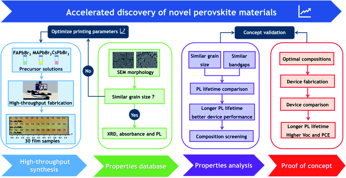 | ||
| Fig. 1 A framework of our proposed composition screening protocol based on high throughput synthesis. | ||
We developed an inkjet printing technique for high throughput manufacture of compact mixed perovskite films in our recent work.12 In order to realize the high throughput synthesis of discontinuous perovskite films with comparable and representative properties, this inkjet printing approach is greatly updated in this work and the corresponding working principle is briefly described below. Fig. 2a illustrates the schematic diagram of the four-channel non-parallel drop-on-demand (DOD) inkjet printer (the photograph in Fig. S2†) including four printheads, four ink cartridges, a mobile flat plate and a programmable control system. During the jetting process, the programmable control system can precisely control the ejected single droplet volume, the droplet number and the location of printed dots as well as the printing sequence of precursors. As depicted in Fig. 2b, except an empty one, three ink cartridges are filled with FAPbBr3, MAPbBr3 and CsPbBr3 precursor solutions, respectively, and the corresponding printheads eject the precursor droplets onto glass substrates in sequence to form mixed precursor films before annealing. It should be pointed out that the whole printing process for mixed perovskite films is fully automated. When we fix the total ejected dots (37![[thin space (1/6-em)]](https://www.rsc.org/images/entities/char_2009.gif) 500) for each mixed film and the jetted single droplet volume (100 pL), the composition of mixed perovskite films is principally determined by the ejected droplet number from each printhead. To demonstrate the impressive control over printing details, a series of FAPbBr3 films are inkjet-printed with decreased ejected dots from left to right, and the resulting film colour gradually changes from dark yellow to light yellow (Fig. 2c). Furthermore, the printing of irregular shaped symbols such as the school logo and the perovskite crystal structure is also achievable, as displayed in Fig. 2d.
500) for each mixed film and the jetted single droplet volume (100 pL), the composition of mixed perovskite films is principally determined by the ejected droplet number from each printhead. To demonstrate the impressive control over printing details, a series of FAPbBr3 films are inkjet-printed with decreased ejected dots from left to right, and the resulting film colour gradually changes from dark yellow to light yellow (Fig. 2c). Furthermore, the printing of irregular shaped symbols such as the school logo and the perovskite crystal structure is also achievable, as displayed in Fig. 2d.
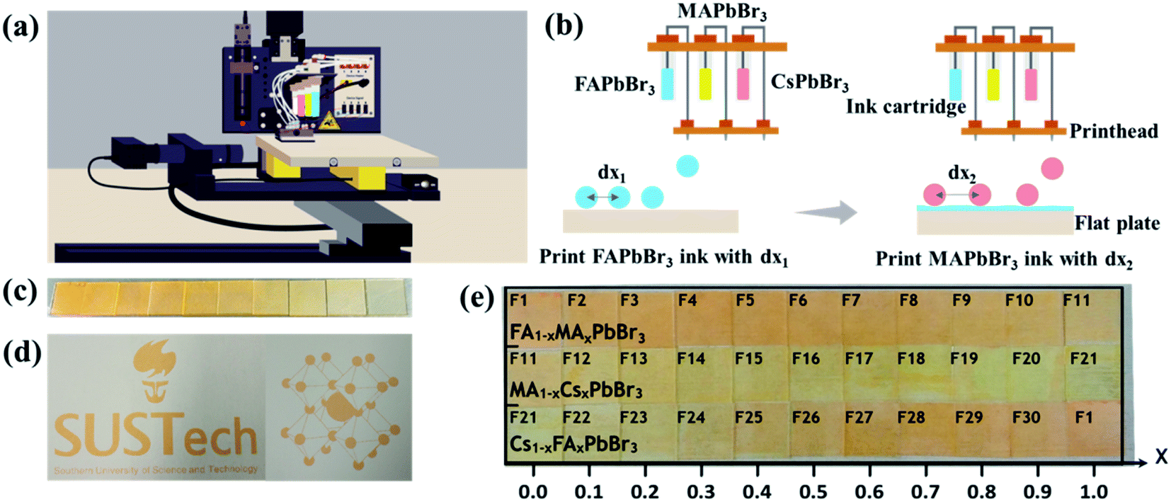 | ||
| Fig. 2 (a) Schematic diagram of the four-channel non-parallel drop-on-demand (DOD) inkjet printer. (b) Schematic diagram of the fabrication of mixed perovskite films (FA1−xMAxPbBr3, MA1−xCsxPbBr3 or Cs1−xFAxPbBr3), where the sequential printing of two different precursors with various volume ratios yields a series of mixed films. (c) Inkjet-printed FAPbBr3 films with decreased ejected dots from left to right. (d) The inkjet-printed school logo (left) and perovskite crystal structure (right). (e) Inkjet-printed FA1−xMAxPbBr3, MA1−xCsxPbBr3 and Cs1−xFAxPbBr3 films marked with numbers from 1 to 30. | ||
As shown in Fig. 2e, any two of FAPbBr3, MAPbBr3 and CsPbBr3 precursors are sequentially printed on glass substrates with mixing ratios between 0% and 100% in 10% steps, producing 30 mixed perovskite films. The as-fabricated films are marked with numbers from 1 to 30 for simplicity. Strikingly, the whole printing process of 30 mixed films was highly reproducible and only took approximately eight minutes, highlighting the rapid production capacity of our inkjet printing technique.
Firstly, scanning electron microscopy (SEM) measurements are performed to investigate the morphology of the above inkjet-printed films, as displayed in Fig. 3a. Although some discontinuous regions exist in most printed films, dense crystalline grains still occupy most of the film surface. These printed films exhibit similar crystal sizes, and the average crystalline size of each film is in the vicinity of 1.5 μm according to the statistical analysis (Fig. 3b). Such a large average crystal size even exceeds that reported for spin-coated films33,38 and can adequately express the basic optoelectronic properties of the corresponding films, and therefore these printed films are enough for the subsequent X-ray diffraction, absorption and PL characterization. More importantly, the very close grain size (Fig. 3b) for these films with different compositions enables us to generate an effective database with perovskite film properties for comparison given the fact that the perovskite grain size can greatly affect the optoelectronic properties of perovskite films, and this resulting database can vastly accelerate the discovery of novel perovskite materials for device applications.
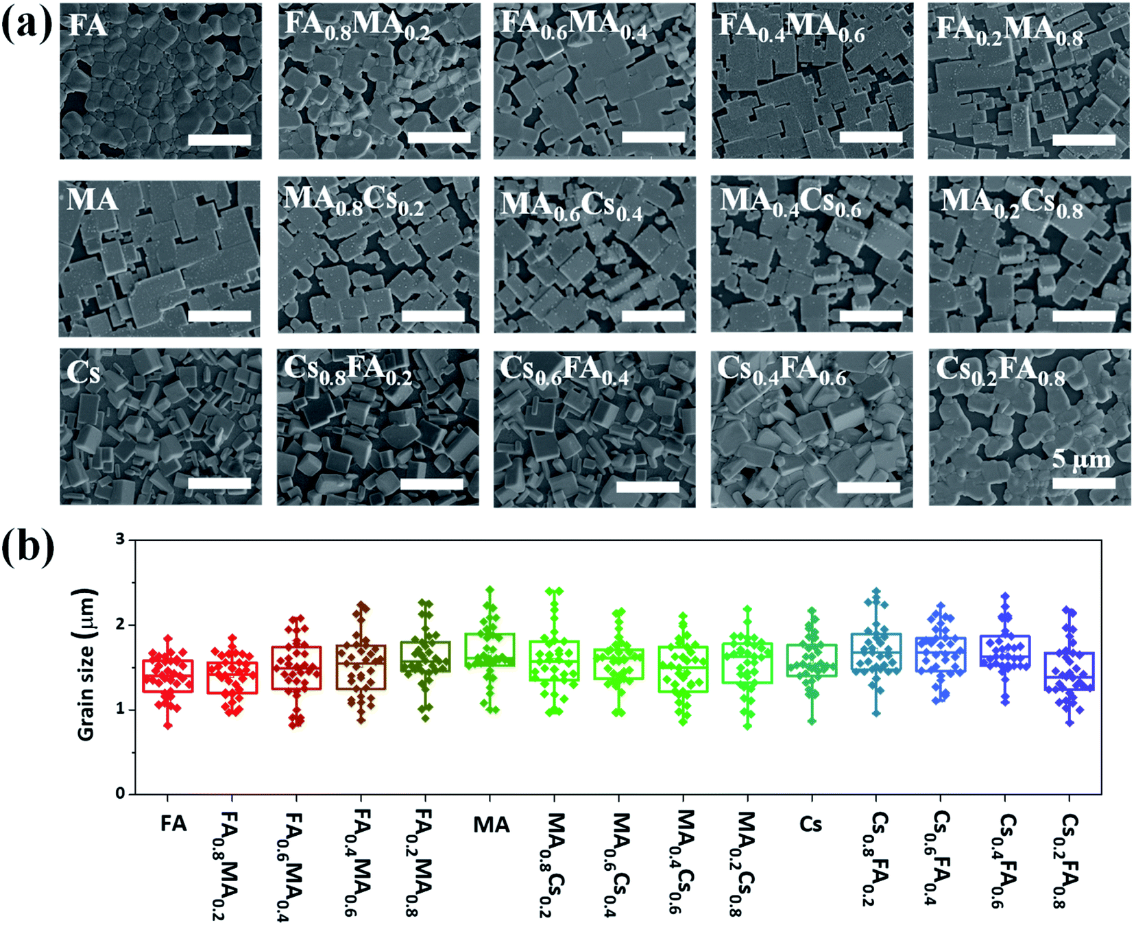 | ||
| Fig. 3 (a) Top-view SEM images of inkjet-printed FA1−xMAxPbBr3, MA1−xCsxPbBr3 and Cs1−xFAxPbBr3 thin films with x = 0, 0.2, 0.4, 0.6, and 0.8, respectively. (b) Statistical distributions of the grain size of these inkjet-printed films. | ||
To examine the crystal phase of these inkjet-printed films, X-ray diffraction (XRD) measurements are implemented. First of all, as shown in Fig. 4a, we compare the XRD patterns of three single-component films (namely FAPbBr3, MAPbBr3 and CsPbBr3). Both FAPbBr3 and MAPbBr3 films exhibit two main diffraction peaks at the 2θ of ∼15° and 30° corresponding to the (100) and (200) lattice planes, indicative of the formation of a cubic structure.41,42 By contrast, an orthorhombic phase is formed in the CsPbBr3 film given the fact that three dominant diffraction peaks at the 2θ of 15.5°, 21.8° and 30.9° can be assigned to (101), (121) and (202) planes, respectively.43 With the increase of MA concentration in FA1−xMAxPbBr3 from 0% to 100% (Fig. S4†), the (100) and (200) diffraction peaks are gradually shifted from 14.9° and 29.8° to 15.2° and 30.4°, respectively, indicating a decreased lattice spacing due to a gradual substitution of FA with smaller MA.44 Additionally, a small amount of PbBr2 indexed to the diffraction peak at ∼12.5° is observed in the FA1−xMAxPbBr3 system, and this phenomenon has been commonly reported in mixed perovskite films.44–46 Similarly, the introduction of 0–100% smaller-sized Cs into FAPbBr3 or MAPbBr3 leads to a shrinkage of the interplanar spacing accompanied by a gradual shift of (100) and (200) main peaks towards slightly higher 2θ angles (Fig. S4†).42,45,47 Meanwhile, the emergence of a characteristic peak located at ∼11.8° means the formation of a parasitic CsPb2Br5 phase in MA1−xCsxPbBr3 and Cs1−xFAxPbBr3, and such a secondary phase generally exists in the Cs-containing tribromide perovskite films according to previous studies.48,49 When the Cs content surpasses 50%, the splitting of a single diffraction peak at ∼30.5° into double peaks probably corresponds to a structural phase transition from the cubic to the orthorhombic structure. The above crystal phase analysis manifests that mixed perovskite films can be reliably manufactured by our high throughput approach.
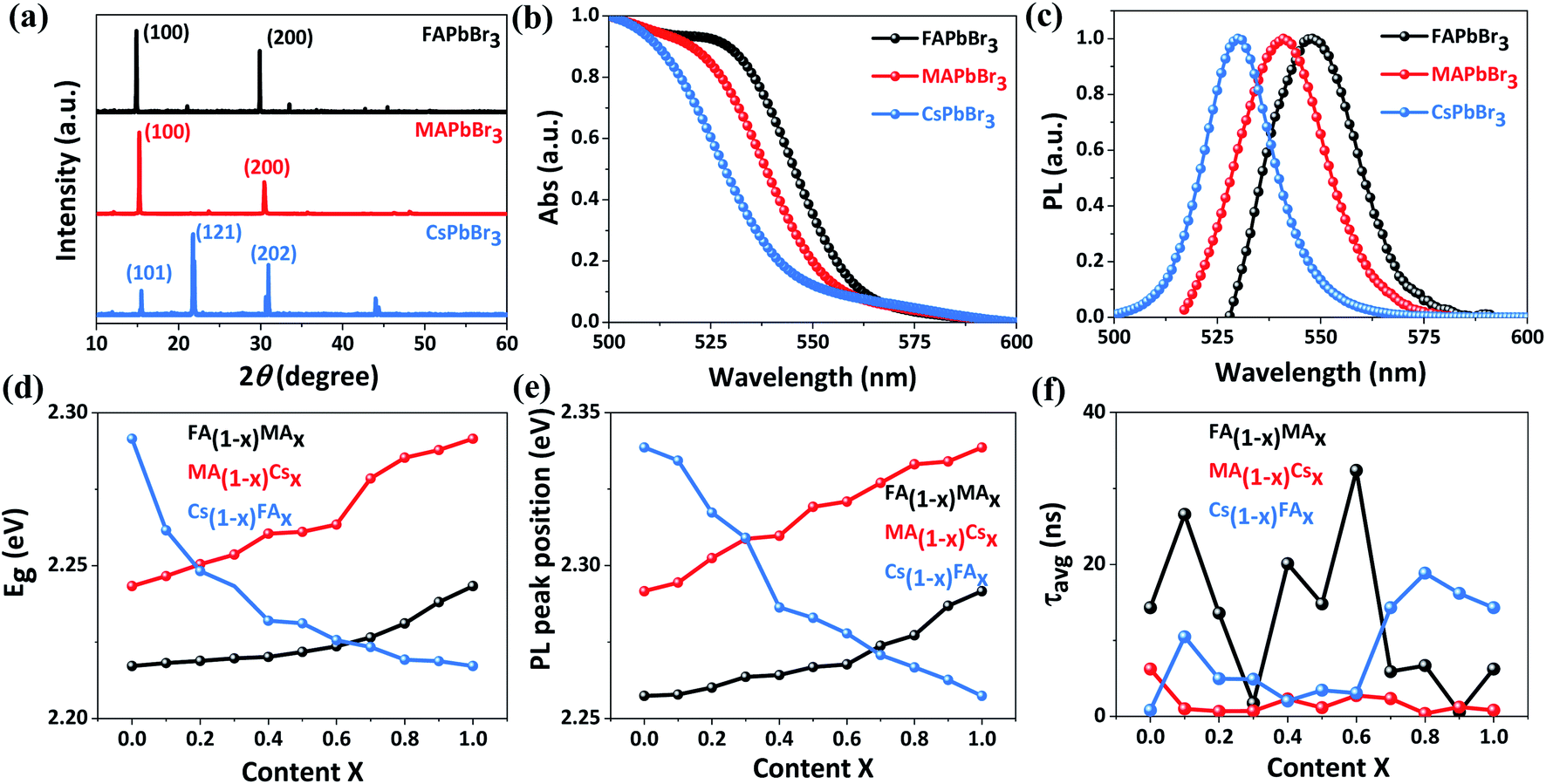 | ||
| Fig. 4 XRD patterns (a), absorbance spectra (b) and PL spectra (c) of inkjet-printed FAPbBr3, MAPbBr3 and CsPbBr3 thin films. Bandgaps (d), PL peak positions (e) and average PL lifetimes (τavg) (f) of inkjet-printed FA1−xMAxPbBr3, MA1−xCsxPbBr3 and Cs1−xFAxPbBr3 films as a function of x. | ||
The absorption and emission properties of these inkjet-printed films are analyzed via absorbance (Abs) and PL spectroscopy measurements. The absorption edges of FA1−xMAxPbBr3, MA1−xCsxPbBr3 and Cs1−xFAxPbBr3 films are compared in Fig. S5,† and the corresponding optical bandgaps (Eg) extracted from Tauc plots (Fig. S6) are summarized in Table S2.† As expected, very close bandgap values of 2.2172, 2.2433 and 2.2915 eV are obtained for FAPbBr3, MAPbBr3 and CsPbBr3 samples, respectively (Fig. 4b). Furthermore, the PL signals of FAPbBr3, MAPbBr3 and CsPbBr3 films peak at 2.2574, 2.2916 and 2.3386 eV (Fig. 4c), respectively. For mixed film samples, their bandgaps range from 2.2172 to 2.2915 eV (Fig. 4d) and the corresponding PL peaks are located within 2.2574–2.3386 eV (Fig. 4e and S7†). The gradual change in the bandgap and PL peak position of these mixed samples is highly consistent with previous findings,42,44,45,47 and also suggests an excellent miscibility of the as-prepared perovskite inks in our high throughput synthesis. This is further confirmed by energy-dispersive X-ray spectrometry (EDS) results (Table S3†), which show small deviations of <4% between the calculated and the experimentally measured Cs/Pb ratio.
To further quantitatively evaluate the charge transport behavior, time-resolved PL spectra of these printed films deposited on glass substrates are recorded and fitted to a bi-exponential decay (Fig. S8†), and the corresponding PL lifetimes are listed in Table S2.† In this case, the bimolecular recombination of long-lived free charges corresponds to the slow decay phase and the fast decay phase is ascribed to trapping into non-radiative trap states,50 and thus we choose the average PL lifetime (τavg) of inkjet-printed films for comparison considering that both decay phases can impact the charge transfer dynamics. For each film, the most representative time-resolved PL spectrum close to average results is used in the calculation of PL lifetimes. As illustrated in Fig. 4f, these samples exhibit obviously different τavg in the range of 0.38–32.36 ns. It should be noted that a longer PL lifetime signifies a lower charge recombination rate and more efficient charge transport, which is very favorable for high-performance photovoltaic applications. In view of similar bandgaps (2.22–2.29 eV) for all film samples, the above average PL lifetime database allows us to efficiently screen these novel compositions and accelerate the discovery of novel tribromide perovskite materials for high-photovoltage and high-efficiency solar cells.
To exemplify the screening role of the PL lifetime database, two perovskite constituents are selected from the 30 tested mixed films to fabricate solar cells for device investigations. Apparently, the FA0.4MA0.6 film exhibits the longest τavg of 32.36 ns out of the 30 samples, and the corresponding device based on FA0.4MA0.6 has great potential to yield a high Voc and PCE. Meanwhile, six samples among the inkjet-printed films have a very short τavg of 0–1 ns, and these film candidates are all Cs-containing except the FA0.1MA0.9 sample. Considering that the Cs-containing tribromide perovskites usually suffer from a low solubility of CsBr in typically used deposition solvents and the resulting great difficulty in the direct adoption of commonly reported solution-processed deposition methods for fabricating high-quality thick films,51 these Cs-containing compositions are excluded for device fabrication and comparison in this study. Consequently, we choose the FA0.4MA0.6 and FA0.1MA0.9 constituents as solar cell absorber materials and further compare the corresponding device performance. Since inkjet-printed FA0.4MA0.6 and FA0.1MA0.9 films with obvious discontinuous regions are not suitable for solar cell manufacture, the following discussion will focus on FA0.4MA0.6 and FA0.1MA0.9 based films and devices deposited by spin coating based on the fact that the spin coating technique normally produces high-performance perovskite solar cells.
Both FA0.4MA0.6 and FA0.1MA0.9 films have a uniform morphology with dense grains as shown in Fig. 5a and b, where the average grain size of the FA0.4MA0.6 film slightly surpasses that of the FA0.1MA0.9 counterpart on the basis of the statistical distribution (Fig. S9†). According to the cross-sectional SEM images, large columnar crystal grains form in both films and the film thickness is measured to be approximately 380 nm. XRD results (Fig. S10†) confirm the formation of a cubic structure in both films.41 The FA0.4MA0.6 and FA0.1MA0.9 films show a bandgap of 2.23 and 2.25 eV according to Tauc plots (Fig. S11†) derived from ultraviolet-visible spectroscopy (Fig. 5c and d), respectively, and the corresponding PL peak are also located at 2.23 and 2.25 eV. The obtained bandgaps and PL peak locations of both films deposited by spin coating are very close to the corresponding values acquired for inkjet-printed films, further emphasizing the feasibility of our high throughput synthesis.
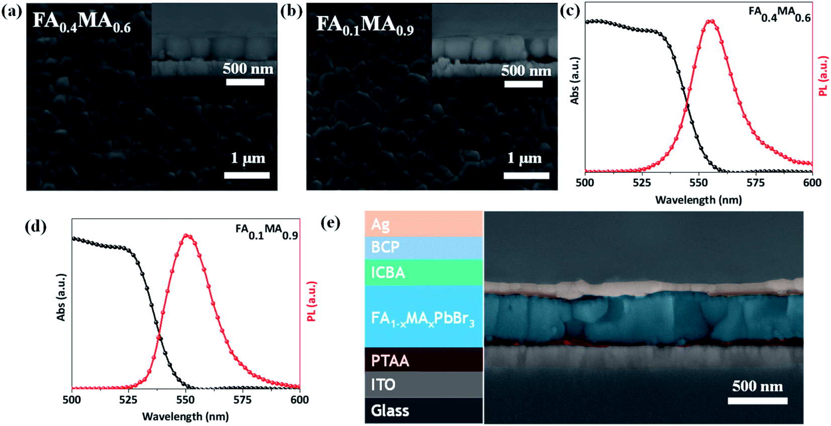 | ||
| Fig. 5 Top-view and cross-sectional SEM images of spin-coated FA0.4MA0.6 (a) and FA0.1MA0.9 (b) films, respectively. Steady-state PL spectra and absorbance spectra of spin-coated FA0.4MA0.6 (c) and FA0.1MA0.9 (d) films, respectively. (e) Cross-sectional SEM image of a typical cell with a structure of ITO/PTAA/perovskite/ICBA/BCP/Ag. | ||
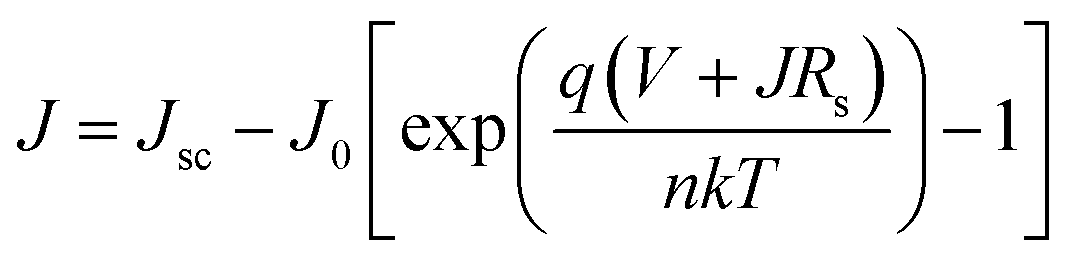
Subsequently, we estimate the photovoltaic performance of FA0.4MA0.6 and FA0.1MA0.9 based devices with an architecture of indium tin oxide (ITO)/poly(bis(4-phenyl)(2,4,6-trimethylphenyl)amine) (PTAA, 20 nm)/perovskite (380 nm)/indene-C60 bisadduct (ICBA, 50 nm)/bathocuproine (BCP, 8 nm)/Ag (100 nm), as depicted in Fig. 5e. Fig. 6a lists the energy levels of MAPbBr3 and selected transport layers as previously reported.52,53 The current density–voltage (J–V) curves of the champion devices measured under standard AM 1.5 G illumination conditions are shown in Fig. 6b, and the corresponding photovoltaic parameters and statistical distributions are summarized in Table 1. The FA0.1MA0.9 based champion device exhibits a short-circuit current density (Jsc) of 6.40 mA cm−2, a Voc of 1.45 V, and a fill factor (FF) of 71.4%, yielding a PCE of 6.62%. By contrast, much better photovoltaic parameters are achieved for the FA0.4MA0.6 champion device, with Jsc = 7.90 mA cm−2, Voc = 1.60 V, FF = 73.2% and PCE = 9.25%, showing a stabilized efficiency of 9.25% at the maximum power output point (Fig. S12†). Such an impressive PCE is among the highest reported efficiencies for tribromide perovskite solar cells.36–40 The remarkably increased Jsc in the FA0.4MA0.6 cell in contrast with the FA0.1MA0.9 counterpart can be mainly attributed to more efficient charge collection (details in Fig. 7b). To better comprehend the enhancements in Voc and FF in the FA0.4MA0.6 device, the series resistance (Rs) and the dark saturated current density (J0) are calculated using the classical diode equation:
 | (1) |
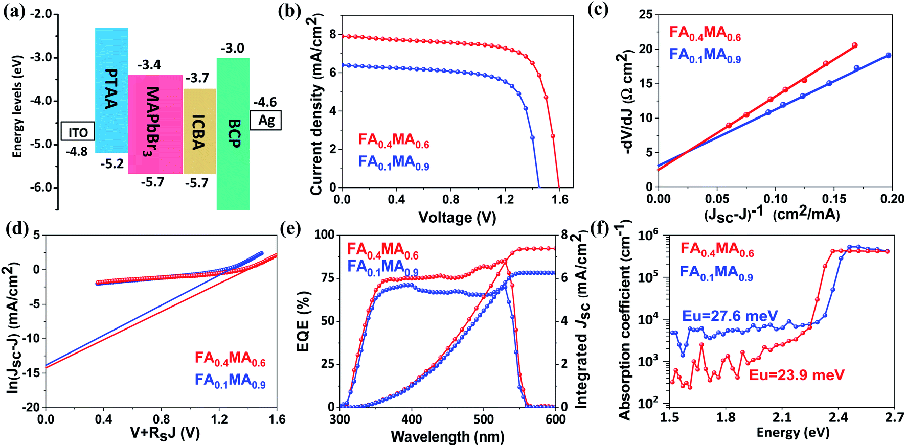 | ||
| Fig. 6 (a) The energy diagram of each layer in the device, and the energy levels of PTAA, MAPbBr3 and ICBA were obtained from previous studies.52,53 (b) J–V characteristics of FA0.4MA0.6 and FA0.1MA0.9 based champion solar cells under AM 1.5 G solar irradiation, where a reverse scan from 1.65 to −0.1 V is performed with a scan rate of 0.1 V s−1. Plots of −dV/dJ versus (Jsc − J)−1 (c) and ln(Jsc − J) versus (V + RsJ) (d) as well as their linear fitting, and both fitting curves are situated around the corresponding Voc. (e) EQE spectra and integrated Jsc. (f) PDS absorbance spectra of FA0.4MA0.6 and FA0.1MA0.9 films coated on quartz substrates. | ||
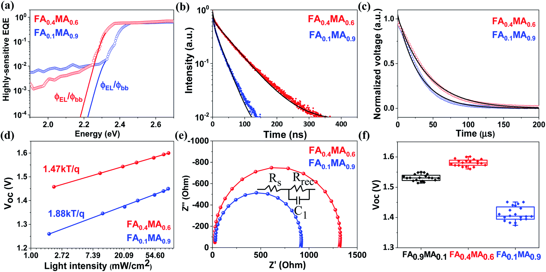 | ||
| Fig. 7 (a) Highly sensitive EQE spectra (dotted line) derived from normalized PDS spectra in Fig. S14,† where the absorption edge is extended by the ratio of the emitted photon flux from electroluminescence to the photon flux for blackbody radiation (solid line). (b) Time-resolved PL spectra of FA0.4MA0.6 and FA0.1MA0.9 films coated on glass substrates. Normalized TPV decay (c), light intensity dependent Voc (d), and Nyquist plots (e) of FA0.4MA0.6 and FA0.1MA0.9 based solar cells, respectively. (f) Voc statistical distributions of FA0.9MA0.1, FA0.4MA0.6 and FA0.1MA0.9 based devices from 20 cells. | ||
It is worth noting that both FA0.4MA0.6 and FA0.1MA0.9 devices have no obvious hysteresis of J–V characteristics with respect to the voltage scan directions (Fig. S13†). The Jsc values obtained from J–V curves are in accordance with those integrated from external quantum efficiency (EQE) spectra (Fig. 6e). Moreover, photothermal deflection spectroscopy (PDS) measurements are carried out to analyze the defects within the sub-bandgap region of both films. Evidently, the sub-bandgap absorption coefficient (α) below 2.2 eV of the FA0.1MA0.9 film is much larger than that of the FA0.4MA0.6 counterpart (Fig. 6f), implying a significant reduction of trap states in the FA0.4MA0.6 film in comparison with the FA0.1MA0.9 film, which benefits the suppression of non-radiative charge recombination. Besides, the electronic disorder of perovskite films can be quantified by the Urbach energy (Eu), which is computed by a single-exponential fit to the PDS spectra at the absorption edge. As a result, the FA0.4MA0.6 film has a much lower Eu (23.9 meV) compared with the FA0.1MA0.9 counterpart (27.6 meV), indicative of a lower level of energetic disorder existing in the FA0.4MA0.6 film.57,58 Such a lower level of energetic disorder enables a reduction of the parasitic charge recombination, consistent with the declining J0 observed above in the FA0.4MA0.6 device.
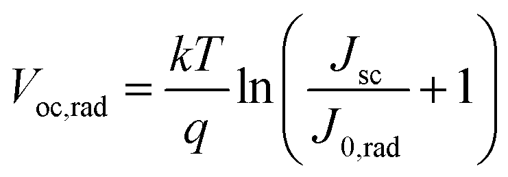
To demonstrate the Voc reproducibility, Voc statistical distributions from 20 cells are also presented in Table 1. The FA0.1MA0.9 device exhibits an average Voc of 1.41 V with a maximum value of 1.45 V. In contrast, the maximum Voc reaches 1.60 V in the FA0.4MA0.6 cell with an average value of 1.58 V, which is among the highest reported Voc values for tribromide perovskite devices (Table S4†). In addition, we further explore the radiative limit of Voc (Voc,rad, namely the Voc limit) for both devices and the corresponding non-radiative recombination losses (ΔVoc), which can be determined from eqn (2) and (3), respectively. Here, Jsc denotes the measured short-circuit current density under one sun illumination, and J0,rad is the saturation current density for radiative recombination. The Voc,rad can be obtained when the absorbed photon flux is balanced exactly by the emitted flux under open-circuit conditions. As shown in Fig. 7a, the highly sensitive EQE spectra of both devices are derived from normalized PDS spectra (Fig. S14†) and can be adopted to compute J0,rad, where the electroluminescence spectra extend the absorption edge into the low-energy region to ensure calculation with sufficiently high resolution (details in the ESI†).59,60 The measured and calculated parameters used for the analysis of non-radiative recombination losses are summarized in Table 2. Amazingly, the Voc,rad obtained is as high as 2.01 V for both FA0.1MA0.9 and FA0.4MA0.6 devices, much higher than the value (1.30–1.33 V) acquired for triiodide perovskite solar cells.61,62 This Voc,rad value is also consistent with that (1.95 V) reported for a MAPbBr3 solar cell in our previous work.33 Accordingly, the FA0.1MA0.9 and FA0.4MA0.6 devices deliver a ΔVoc value of 0.56 and 0.41 V, respectively, suggesting a much lower level of non-radiative recombination losses existing in the FA0.4MA0.6 stack. Evidently, these tribromide devices suffer more from non-radiative recombination losses than their triiodide analogues which were reported with ΔVoc values of 0.1–0.2 V.59,63 This comparison also means that the Voc for these devices may be further increased if non-radiative recombination can be remarkably suppressed even further.
 | (2) |
| ΔVoc = Voc,rad − Voc | (3) |
| Active layer | FA0.4MA0.6 | FA0.1MA0.9 |
|---|---|---|
| J sc [mA cm−2] | 7.90 | 6.40 |
| J 0,rad [mA cm−2] | 1.6 × 10⁻³³ | 9.3 × 10⁻³⁴ |
| V oc,rad [V] | 2.01 | 2.01 |
| V oc [V] measured | 1.60 | 1.45 |
| ΔVoc [V] (Voc,rad − Voc) | 0.41 | 0.56 |
In order to further comprehend the distinction in device performance, the charge transport characteristics are explored via recording the time-resolved PL spectra of both films deposited on glass substrates, as displayed in Fig. 7b. A bi-exponential fitting to the time-resolved PL spectra gives the corresponding PL lifetimes (Table S5†). The FA0.1MA0.9 film shows an average PL lifetime of 13.5 ns, while a much longer average PL lifetime (37.3 ns) is achieved in the case of the FA0.4MA0.6 film, in agreement with trends observed in the PL lifetime database for inkjet-printed films. The extension of PL lifetimes in the FA0.4MA0.6 film means better charge transport to a large extent, contributing to a higher photocurrent in devices. Additionally, transient photovoltage (TPV) measurements are conducted to determine the charge recombination lifetime of both devices, as illustrated in Fig. 7c. The normalized photovoltage of the FA0.4MA0.6 device decays with a long lifetime of 42.2 μs, which is almost 1.5 times that (30.4 μs) of the FA0.1MA0.9 counterpart, indicating lower charge recombination losses in the FA0.4MA0.6 cell.64,65
To gain further insight into the relationship between charge recombination and device performance with different absorber layers, the charge recombination mechanism is evaluated on the basis of light intensity dependent Voc and electrochemical impedance spectroscopy (EIS). Normally, the slope of Vocversus the natural logarithm of light intensity deviating from kT/q manifests the existence of trap-assisted charge recombination.66–68 As depicted in Fig. 7d, the corresponding slope for FA0.1MA0.9 and FA0.4MA0.6 devices is determined to be 1.88kT/q and 1.47kT/q, respectively. The smaller slope for the FA0.4MA0.6 device suggests a more effective suppression of charge recombination through trap states, in good accordance with the decreased defects in the FA0.4MA0.6 film, thus leading to a higher Voc. Fig. 7e presents the Nyquist plots from impedance spectra of both devices and the corresponding circuit model. The FA0.4MA0.6 device has a much larger recombination resistance (Rrec) (1285 Ω) than the FA0.1MA0.9 counterpart (879 Ω), suggesting that the charge recombination process can be more effectively suppressed in the FA0.4MA0.6 device.69,70 In general, substantially decreased charge recombination losses exist in the FA0.4MA0.6 device in comparison with the FA0.1MA0.9 counterpart on the basis of TPV and light intensity dependent Voc as well as EIS results, which inevitably contribute to its better device performance.
In order to further confirm the validity of the above PL lifetime database for novel composition screening, we employ another new composition (FA0.9MA0.1) as an example to check the achievable Voc, given the fact that the average PL lifetime of the FA0.9MA0.1 film is ranked second (26.58 ns) among all inkjet-printed samples. According to the statistical analysis from 20 cells, the FA0.9MA0.1 device yields a Voc of 1.53 ± 0.02 V with a maximum value of 1.55 V (Fig. 7f). These Voc values are slightly smaller than that (1.58 ± 0.02) of the FA0.4MA0.6 device, but obviously outperform that (1.41 ± 0.04) obtained for the FA0.1MA0.9 counterpart. This result further supports that our PL lifetime database can indeed screen out novel tribromide perovskites for high-photovoltage solar cells. With this we conclude that our proposed composition screening protocol based on high throughput inkjet printing can effectively accelerate the discovery of novel perovskite materials for device applications.
3 Conclusion
In summary, we have developed a highly efficient composition screening protocol based on high throughput inkjet printing of discontinuous rather than compact perovskite films with representative and comparable properties to accelerate the discovery of novel tribromide perovskites for high-photovoltage solar cells. Specifically, the sequential inkjet printing of three precursor solutions yields 30 mixed tribromide perovskite films with similar bandgaps rapidly and automatically, where the good control of the crystallization behaviour produces a very close grain size for all samples. Thus, the corresponding PL lifetime database enables us to efficiently screen and identify novel compositions for high-photovoltage solar cells. To verify this, two constituents of FA0.4MA0.6 and FA0.1MA0.9 with a long (32.36 ns) and short (0.57 ns) average PL lifetime, respectively, are selected out of the 30 tested films as device analysis. As anticipated, the FA0.4MA0.6 device achieves a high Voc of 1.60 V along with a peak PCE of 9.25%, which greatly outperform those (1.45 V and 6.62%) acquired for the FA0.1MA0.9 counterpart. The as-obtained Voc of 1.60 V is among the highest reported Voc values for tribromide perovskite devices, and more importantly, the Voc,rad is estimated to be as high as 2.01 V for both devices for the first time. The greatly enhanced device performance (especially Voc) can be mainly attributed to the reduced trap states, lower level of energetic disorder and more efficient charge transport as well as considerably decreased charge recombination losses. In addition, the validity of the PL lifetime database is further confirmed by a high Voc of 1.55 V achieved in devices based on another novel FA0.9MA0.1 composition with a long average PL lifetime. These results highlight that our proposed high throughput composition screening approach can effectively and efficiently accelerate the discovery of novel perovskites for advanced device applications.Author contributions
X. Z. W., S. H. Y., and B. M. X. designed and directed the study. S. C. and L. H. Z. conceived and performed the film and device fabrication work. Z. Q. Z. and S. K. S. performed the PDS measurements. Y. L. L. and Y. L. conducted the PL measurements. W. Z. C. and H. Y. L. contributed to the TPV measurements and analysis. Q. L. L. and B. Z. carried out the SEM measurements. Y. C. Q., T. Y., and J. R. conducted the XRD and absorbance measurements. S. M. C., X. D. X., and S. Y. D. provided advice and expertise. S. C. and B. M. X. wrote the original draft of the manuscript, and all authors contributed to the discussion.Conflicts of interest
The authors declare no competing financial interest.Acknowledgements
This work was supported by the National Key Research and Development Program of China (2016YFA0202400 and 2016YFA0202404), the National Natural Science Foundation of China (62004089, 62004091 and U19A2089), the Guangdong Basic and Applied Basic Research Foundation (2019A1515110439 and 2019B1515120083), the Shenzhen Science and Technology Program (JCYJ20190809150811504 and KQTD2015033110182370), the HKRGC General Research Funds (16312216), the Shenzhen & Hong Kong Joint Research Program (SGLH20180622092406130), the Shenzhen Engineering Research and Development Center for Flexible Solar Cells Project funding from the Shenzhen Development and Reform Committee (2019-126), and the Guangdong-Hong Kong-Macao Joint Laboratory (2019B121205001).References
- N. J. Jeon, J. H. Noh, W. S. Yang, Y. C. Kim, S. Ryu, J. Seo and S. I. Seok, Nature, 2015, 517, 476–480 CrossRef CAS PubMed
.
- M. Liu, M. B. Johnston and H. J. Snaith, Nature, 2013, 501, 395–398 CrossRef CAS PubMed
- N. J. Jeon, J. H. Noh, Y. C. Kim, W. S. Yang, S. Ryu and S. I. Seok, Nat. Mater., 2014, 13, 897–903 CrossRef CAS PubMed
- Q. Jiang, Y. Zhao, X. Zhang, X. Yang, Y. Chen, Z. Chu, Q. Ye, X. Li, Z. Yin and J. You, Nat. Photonics, 2019, 13, 460–466 CrossRef CAS
- H. Min, M. Kim, S.-U. Lee, H. Kim, G. Kim, K. Choi, J. H. Lee and S. I. Seok, Science, 2019, 366, 749–753 CrossRef CAS PubMed
- E. H. Jung, N. J. Jeon, E. Y. Park, C. S. Moon, T. J. Shin, T.-Y. Yang, J. H. Noh and J. Seo, Nature, 2019, 567, 511–515 CrossRef CAS PubMed
- M. Kim, G.-H. Kim, T. K. Lee, I. W. Choi, H. W. Choi, Y. Jo, Y. J. Yoon, J. W. Kim, J. Lee, D. Huh, H. Lee, S. K. Kwak, J. Y. Kim and D. S. Kim, Joule, 2019, 3, 2179–2192 CrossRef CAS
- J. J. Yoo, S. Wieghold, M. C. Sponseller, M. R. Chua, S. N. Bertram, N. T. P. Hartono, J. S. Tresback, E. C. Hansen, J.-P. Correa-Baena, V. Bulović, T. Buonassisi, S. S. Shin and M. G. Bawendi, Energy Environ. Sci., 2019, 12, 2192–2199 RSC
- J. Kirman, A. Johnston, D. A. Kuntz, M. Askerka, Y. Gao, P. Todorović, D. Ma, G. G. Privé and E. H. Sargent, Matter, 2020, 2, 938–947 CrossRef
- S. Chen, Y. Hou, H. Chen, X. Tang, S. Langner, N. Li, T. Stubhan, I. Levchuk, E. Gu, A. Osvet and C. J. Brabec, Adv. Energy Mater., 2018, 8, 1701543 CrossRef
- S. Sun, N. T. P. Hartono, Z. D. Ren, F. Oviedo, A. M. Buscemi, M. Layurova, D. X. Chen, T. Ogunfunmi, J. Thapa, S. Ramasamy, C. Settens, B. L. DeCost, A. G. Kusne, Z. Liu, S. I. P. Tian, I. M. Peters, J.-P. Correa-Baena and T. Buonassisi, Joule, 2019, 3, 1437–1451 CrossRef CAS
- S. Chen, L. Zhang, L. Yan, X. Xiang, X. Zhao, S. Yang and B. Xu, Adv. Funct. Mater., 2019, 29, 1905487 CrossRef CAS
- W. Nie, H. Tsai, R. Asadpour, J.-C. Blancon, A. J. Neukirch, G. Gupta, J. J. Crochet, M. Chhowalla, S. Tretiak, M. A. Alam, H.-L. Wang and A. D. Mohite, Science, 2015, 347, 522–525 CrossRef CAS PubMed
- F. Guo, S. Qiu, J. Hu, H. Wang, B. Cai, J. Li, X. Yuan, X. Liu, K. Forberich, C. J. Brabec and Y. Mai, Adv. Sci., 2019, 6, 1901067 CrossRef PubMed
- F. Guo, W. He, S. Qiu, C. Wang, X. Liu, K. Forberich, C. J. Brabec and Y. Mai, Adv. Funct. Mater., 2019, 29, 1900964 CrossRef
- C. Li, Y. Pan, J. Hu, S. Qiu, C. Zhang, Y. Yang, S. Chen, X. Liu, C. J. Brabec, M. K. Nazeeruddin, Y. Mai and F. Guo, ACS Energy Lett., 2020, 5, 1386–1395 CrossRef CAS
- W.-Q. Wu, Q. Wang, Y. Fang, Y. Shao, S. Tang, Y. Deng, H. Lu, Y. Liu, T. Li, Z. Yang, A. Gruverman and J. Huang, Nat. Commun., 2018, 9, 1625 CrossRef PubMed
- J. G. Tait, S. Manghooli, W. Qiu, L. Rakocevic, L. Kootstra, M. Jaysankar, C. A. Masse de la Huerta, U. W. Paetzold, R. Gehlhaar, D. Cheyns, P. Heremans and J. Poortmans, J. Mater. Chem. A, 2016, 4, 3792–3797 RSC
- M. Park, W. Cho, G. Lee, S. C. Hong, M.-c. Kim, J. Yoon, N. Ahn and M. Choi, Small, 2019, 15, 1804005 CrossRef PubMed
- M. Bag, Z. Jiang, L. A. Renna, S. P. Jeong, V. M. Rotello and D. Venkataraman, Mater. Lett., 2016, 164, 472–475 CrossRef CAS
- X. Peng, J. Yuan, S. Shen, M. Gao, A. S. R. Chesman, H. Yin, J. Cheng, Q. Zhang and D. Angmo, Adv. Funct. Mater., 2017, 27, 1703704 CrossRef
- C. Liang, P. Li, H. Gu, Y. Zhang, F. Li, Y. Song, G. Shao, N. Mathews and G. Xing, Sol. RRL, 2018, 2, 1700217 CrossRef
- A. J. Huckaba, Y. Lee, R. Xia, S. Paek, V. C. Bassetto, E. Oveisi, A. Lesch, S. Kinge, P. J. Dyson, H. Girault and M. K. Nazeeruddin, Energy Technol., 2019, 7, 317–324 CrossRef CAS
- H. Eggers, F. Schackmar, T. Abzieher, Q. Sun, U. Lemmer, Y. Vaynzof, B. S. Richards, G. Hernandez-Sosa and U. W. Paetzold, Adv. Energy Mater., 2020, 10, 1903184 CrossRef CAS
- S.-G. Li, K.-J. Jiang, M.-J. Su, X.-P. Cui, J.-H. Huang, Q.-Q. Zhang, X.-Q. Zhou, L.-M. Yang and Y.-L. Song, J. Mater. Chem. A, 2015, 3, 9092–9097 RSC
- J. H. Heo and S. H. Im, Adv. Mater., 2015, 28, 5121–5125 CrossRef PubMed
- J. Luo, J.-H. Im, M. T. Mayer, M. Schreier, M. K. Nazeeruddin, N.-G. Park, S. D. Tilley, H. J. Fan and M. Grätzel, Science, 2014, 345, 1593–1596 CrossRef CAS PubMed
- M. Schreier, L. Curvat, F. Giordano, L. Steier, A. Abate, S. M. Zakeeruddin, J. Luo, M. T. Mayer and M. Grätzel, Nat. Commun., 2015, 6, 7326 CrossRef CAS PubMed
- C. Zhang, Y.-N. Lu, W.-Q. Wu and L. Wang, Nano Energy, 2021, 81, 105634 CrossRef CAS
- W. Feng, C. Zhang, J.-X. Zhong, L. Ding and W.-Q. Wu, Chem. Commun., 2020, 56, 5006–5009 RSC
- J.-X. Zhong, J.-F. Liao, Y. Jiang, L. Wang, D.-B. Kuang and W.-Q. Wu, J. Mater. Chem. A, 2020, 8, 9743–9752 RSC
- N. Arora, S. Orlandi, M. I. Dar, S. Aghazada, G. Jacopin, M. Cavazzini, E. Mosconi, P. Gratia, F. De Angelis, G. Pozzi, M. Graetzel and M. K. Nazeeruddin, ACS Energy Lett., 2016, 1, 107–112 CrossRef CAS
- S. Chen, Y. Hou, H. Chen, M. Richter, F. Guo, S. Kahmann, X. Tang, T. Stubhan, H. Zhang, N. Li, N. Gasparini, C. O. R. Quiroz, L. S. Khanzada, G. J. Matt, A. Osvet and C. J. Brabec, Adv. Energy Mater., 2016, 6, 1600132 CrossRef
- C. Zuo and L. Ding, Adv. Energy Mater., 2017, 7, 1601193 CrossRef
- C.-G. Wu, C.-H. Chiang and S. H. Chang, Nanoscale, 2016, 8, 4077–4085 RSC
- N. K. Noel, B. Wenger, S. N. Habisreutinger, J. B. Patel, T. Crothers, Z. Wang, R. J. Nicholas, M. B. Johnston, L. M. Herz and H. J. Snaith, ACS Energy Lett., 2018, 3, 1233–1240 CrossRef CAS
- J. H. Heo, D. H. Song and S. H. Im, Adv. Mater., 2014, 26, 8179–8183 CrossRef CAS PubMed
- Y. Liang, Y. Wang, C. Mu, S. Wang, X. Wang, D. Xu and L. Sun, Adv. Energy Mater., 2018, 8, 1701159 CrossRef
- J. Duan, Y. Zhao, X. Yang, Y. Wang, B. He and Q. Tang, Adv. Energy Mater., 2018, 8, 1802346 CrossRef
- X. Hu, X.-F. Jiang, X. Xing, L. Nian, X. Liu, R. Huang, K. Wang, H.-L. Yip and G. Zhou, Sol. RRL, 2018, 2, 1800083 CrossRef
- A. Kojima, K. Teshima, Y. Shirai and T. Miyasaka, J. Am. Chem. Soc., 2009, 131, 6050–6051 CrossRef CAS PubMed
- X. Zhang, H. Liu, W. Wang, J. Zhang, B. Xu, K. L. Karen, Y. Zheng, S. Liu, S. Chen, K. Wang and X. W. Sun, Adv. Mater., 2017, 29, 1606405 CrossRef PubMed
- H. Cho, C. Wolf, J. S. Kim, H. J. Yun, J. S. Bae, H. Kim, J.-M. Heo, S. Ahn and T.-W. Lee, Adv. Mater., 2017, 29, 1700579 CrossRef PubMed
- B. Slimi, M. Mollar, B. Marí and R. Chtourou, J. Electron. Mater., 2019, 48, 8014–8023 CrossRef CAS
- H. Cho, J. S. Kim, C. Wolf, Y.-H. Kim, H. J. Yun, S.-H. Jeong, A. Sadhanala, V. Venugopalan, J. W. Choi, C.-L. Lee, R. H. Friend and T.-W. Lee, ACS Nano, 2018, 12, 2883–2892 CrossRef CAS PubMed
- C. Yi, J. Luo, S. Meloni, A. Boziki, N. Ashari-Astani, C. Grätzel, S. M. Zakeeruddin, U. Röthlisberger and M. Grätzel, Energy Environ. Sci., 2016, 9, 656–662 RSC
- A. A. Sutanto, V. I. E. Queloz, I. Garcia-Benito, K. Laasonen, B. Smit, M. K. Nazeeruddin, O. A. Syzgantseva and G. Grancini, APL Mater., 2019, 7, 041110 CrossRef
- C. Tenailleau, S. Aharon, B.-E. Cohen and L. Etgar, Nanoscale Adv., 2019, 1, 147–153 RSC
- G. Tong, M. Jiang, D.-Y. Son, L. Qiu, Z. Liu, L. K. Ono and Y. Qi, ACS Appl. Mater. Interfaces, 2020, 12, 14185–14194 CrossRef CAS PubMed
- Y. Yamada, T. Yamada, A. Shimazaki, A. Wakamiya and Y. Kanemitsu, J. Phys. Chem. Lett., 2016, 7, 1972–1977 CrossRef CAS PubMed
- J. B. Hoffman, G. Zaiats, I. Wappes and P. V. Kamat, Chem. Mater., 2017, 29, 9767–9774 CrossRef CAS
- Y. He, H.-Y. Chen, J. Hou and Y. Li, J. Am. Chem. Soc., 2010, 132, 1377–1382 CrossRef CAS PubMed
- S. Ryu, J. H. Noh, N. J. Jeon, Y. Chan Kim, W. S. Yang, J. Seo and S. I. Seok, Energy Environ. Sci., 2014, 7, 2614–2618 RSC
- W. Kong, W. Li, C. Liu, H. Liu, J. Miao, W. Wang, S. Chen, M. Hu, D. Li, A. Amini, S. Yang, J. Wang, B. Xu and C. Cheng, ACS Nano, 2019, 13, 1625–1634 CrossRef CAS PubMed
- S. Chen, N. Shen, L. Zhang, L. Zhang, S. H. Cheung, S. Chen, S. K. So and B. Xu, Adv. Funct. Mater., 2020, 30, 1907759 CrossRef CAS
- J. You, Y. Yang, Z. Hong, T.-B. Song, L. Meng, Y. Liu, C. Jiang, H. Zhou, W.-H. Chang, G. Li and Y. Yang, Appl. Phys. Lett., 2014, 105, 183902 CrossRef
- X. Meng, J. Zhou, J. Hou, X. Tao, S. H. Cheung, S. K. So and S. Yang, Adv. Mater., 2018, 30, 1706975 CrossRef PubMed
- A. Ng, Z. Ren, H. Hu, P. W. K. Fong, Q. Shen, S. H. Cheung, P. Qin, J.-W. Lee, A. B. Djurišić, S. K. So, G. Li, Y. Yang and C. Surya, Adv. Mater., 2018, 30, 1804402 CrossRef PubMed
- D. Luo, W. Yang, Z. Wang, A. Sadhanala, Q. Hu, R. Su, R. Shivanna, G. F. Trindade, J. F. Watts, Z. Xu, T. Liu, K. Chen, F. Ye, P. Wu, L. Zhao, J. Wu, Y. Tu, Y. Zhang, X. Yang, W. Zhang, R. H. Friend, Q. Gong, H. J. Snaith and R. Zhu, Science, 2018, 360, 1442–1446 CrossRef CAS PubMed
- T. Kirchartz and U. Rau, J. Appl. Phys., 2007, 102, 104510 CrossRef
- W. Tress, N. Marinova, O. Inganäs, M. K. Nazeeruddin, S. M. Zakeeruddin and M. Graetzel, Adv. Energy Mater., 2015, 5, 1400812 CrossRef
- K. Tvingstedt, O. Malinkiewicz, A. Baumann, C. Deibel, H. J. Snaith, V. Dyakonov and H. J. Bolink, Sci. Rep., 2014, 4, 6071 CrossRef CAS PubMed
- M. Saliba, T. Matsui, K. Domanski, J.-Y. Seo, A. Ummadisingu, S. M. Zakeeruddin, J.-P. Correa-Baena, W. R. Tress, A. Abate, A. Hagfeldt and M. Grätzel, Science, 2016, 354, 206–209 CrossRef CAS PubMed
- J. Tian, Q. Xue, X. Tang, Y. Chen, N. Li, Z. Hu, T. Shi, X. Wang, F. Huang, C. J. Brabec, H.-L. Yip and Y. Cao, Adv. Mater., 2019, 31, 1901152 CrossRef PubMed
- W. Chen, Y. Wu, J. Fan, A. B. Djurišić, F. Liu, H. W. Tam, A. Ng, C. Surya, W. K. Chan, D. Wang and Z. B. He, Adv. Energy Mater., 2018, 8, 1703519 CrossRef
- S. Chen, N. Shen, L. Zhang, W. Kong, L. Zhang, C. Cheng and B. Xu, J. Mater. Chem. A, 2019, 7, 9542–9549 RSC
- L. Yan, Q. Xue, M. Liu, Z. Zhu, J. Tian, Z. Li, Z. Chen, Z. Chen, H. Yan, H.-L. Yip and Y. Cao, Adv. Mater., 2018, 30, 1802509 CrossRef PubMed
- B. Zhao, M. Abdi-Jalebi, M. Tabachnyk, H. Glass, V. S. Kamboj, W. Nie, A. J. Pearson, Y. Puttisong, K. C. Gödel, H. E. Beere, D. A. Ritchie, A. D. Mohite, S. E. Dutton, R. H. Friend and A. Sadhanala, Adv. Mater., 2017, 29, 1604744 CrossRef PubMed
- S. Ahmad, P. Fu, S. Yu, Q. Yang, X. Liu, X. Wang, X. Wang, X. Guo and C. Li, Joule, 2019, 3, 794–806 CrossRef CAS
- J. Ma, G. Yang, M. Qin, X. Zheng, H. Lei, C. Chen, Z. Chen, Y. Guo, H. Han, X. Zhao and G. Fang, Adv. Sci., 2017, 4, 1700031 CrossRef PubMed
Footnotes |
| † Electronic supplementary information (ESI) available. See DOI: 10.1039/d1ta06594g |
| ‡ These authors contributed equally to this work. |
| This journal is © The Royal Society of Chemistry 2021 |