
 Open Access Article
 This Open Access Article is licensed under a Creative Commons Attribution-Non Commercial 3.0 Unported Licence
Two-step MAPbI3 deposition by low-vacuum proximity-space-effusion for high-efficiency inverted semitransparent perovskite solar cells†
Emanuele
Smecca
 a,
Vitantonio
Valenzano
be,
Salvatore
Valastro
ac,
Ioannis
Deretzis
a,
Giovanni
Mannino
a,
Graziella
Malandrino
d,
Gianluca
Accorsi
e,
Silvia
Colella
f,
Aurora
Rizzo
e,
Antonino
La Magna
a,
Andrea
Listorti
*eg and
Alessandra
Alberti
*a
a,
Vitantonio
Valenzano
be,
Salvatore
Valastro
ac,
Ioannis
Deretzis
a,
Giovanni
Mannino
a,
Graziella
Malandrino
d,
Gianluca
Accorsi
e,
Silvia
Colella
f,
Aurora
Rizzo
e,
Antonino
La Magna
a,
Andrea
Listorti
*eg and
Alessandra
Alberti
*a
aCNR-IMM Zona Industriale, Strada VIII 5, 95121 Catania, Italy. E-mail: alessandra.alberti@imm.cnr.it
bDipartimento di Matematica e Fisica “E. De Giorgi”, Università del Salento, Campus Ecotekne, Via Arnesano, 73100 Lecce, Italy
cDipartimento di Fisica e Astronomia, Università degli Studi di Catania, Via S. Sofia 64, 95123 Catania, Italy
dDipartimento di Scienze Chimiche, Università degli Studi di Catania, V.le A. Doria, 95125 Catania, Italy
eCNR NANOTEC, Institute of Nanotechnology, c/o Campus Ecotekne, via Monteroni, 73100 Lecce, Italy
fCNR NANOTEC, Institute of Nanotechnology, c/o Department of Chemistry, University of Bari ‘Aldo Moro’, via Orabona 4, 70126 Bari, Italy
gDepartment of Chemistry, University of Bari “Aldo Moro”, via Orabona 4, Bari, 70126, Italy. E-mail: andrea.listorti@uniba.it
First published on 25th June 2021
Abstract
Halide perovskite solar cells can combine high photoconversion efficiency with high transmittance. Herein, we describe an innovative vacuum deposition method to prepare thin CH3NH3PbI3 (MAPbI3) layers for semitransparent perovskite solar cells. The method is based on two-step Low-Vacuum Proximity-Space-Effusion (LV-PSE: working pressure 2–4 × 10⁻² mbar; source-substrate distance 1–3 cm) that guarantees high-quality at low production costs. The process parameter optimization was validated by theoretical calculation. We show that, during the process of CH3NH3I (MAI) deposition (second step) on PbI2 (first step) at a given substrate temperature, the conversion of the PbI2 film to MAPbI3 occurs from the top surface inward via an adsorption–incorporation–migration mechanism guided by the gradient of energetic MAI concentration. The quality of the final layer arises from this progressive conversion that also exploits the lattice order (texture) of the mother PbI2 layer. Finally, p–i–n solar cells were prepared using ITO/PTAA/MAPbI3/PCBM-BCP/Al architectures with a photo-active layer thickness of 150 nm. This layer, characterized by an Average Visible Transmittance (AVT) as high as 20%, produced an average efficiency of 14.4% that is a remarkable result considering the transparency vs. efficiency countertrend that indeed demands to boost the quality of the material. Very importantly, we demonstrated that a further down scalability of the MAPbI3 layer is feasible as proved by reducing the thickness down to 80 nm. In this specific case, the devices showed an average efficiency of 12.9% withstanding an AVT of 32.8%. This notable efficiency recorded on those extremely thin layers thus benefits from the exclusive quality of the MAPbI3 grown with the developed method.
1. Introduction
Hybrid organic–inorganic perovskites are worldwide one of the most investigated materials today, due to their unique properties impacting various fields such as photovoltaics,1–4 Light Emission Devices (LEDs)5,6 and photodetectors.7–9 In PV, thanks to the wide absorption range and excellent charge carrier lifetime and diffusion10 of the material, Perovskite Solar Cells (PSCs) were able to reach an exceptional goal of 25.5% (ref. 11) just ten years after the first publication of Miyasaka et al.12 in 2009. All their exceptional properties, derived from the possibility of preparing high quality films in terms of crystallinity, thickness and low defect density, are strictly related.13–15 Counterbalancing those advantages, there are still open issues related to the device stability particularly under humid air ambient,16,17 and to the realization of high-quality large area films via wet deposition approaches, which cool down their attractiveness from the industrial point of view. A great effort was dedicated to improving the stability18,19 and crystallinity20 of perovskite polycrystalline films, but most of the work was focused on spin coating or other solvent dependent methods.In this perspective, although vacuum deposition methods are more suitable in terms of industrial throughput, they were less investigated, despite some seminal work21–24 demonstrating how hybrid organic inorganic perovskite films prepared by co-evaporation possess higher stability and performances with respect to films prepared by spin coating techniques. In this context, a record efficiency of 20.8% was achieved using high vacuum conditions, (∼1 × 10⁻⁶ mbar) by Perez del Rey et al.25 with a co-evaporation of MAI and PbI2 for a 590 nm-thick layer of MAPbI3. More recently, Arivazhgan et al.26 have studied in detail the role of vapor pressure in a range of high-vacuum (HV) conditions between 5.6 × 10⁻⁵ torr and 5.6 × 10⁻⁶ torr finding the best condition at 3.3 × 10⁻⁵ torr that allowed a 350-thick MAPbI3 layer achieving 15.74% cell efficiency. Guo et al.27 used the well-known closed space sublimation (CSS) technique for the deposition of organic materials to convert pristine spin-coated PbI2 into MAPbI3 by the sublimation of MAI powder at a very short distance (∼1 mm). They obtained a best efficiency of 16.2% with a 4 mm2 active area device. Gu et al.28 exploited the same technique but depositing 820 nm thick films of mixed lead halide perovskite, thus achieving a remarkable 20.44% efficiency on a 0.07 cm2 active solar cell area. Nonetheless, the limitation of the need of a solution processing step for the deposition of PbI2 proceeding MAI deposition still remains in CSS. Another approach was proposed by Ng et al.29 consisting of a deposition of a multilayered stack of PbI2 and MAI with a post-annealing treatment to form the MAPbI3 film. With this technique, they were able to reach an 11.4% efficiency using 473 nm-thick MAPbI3 layers. Useful insights can be found in the paper by Baekbo et al.30 wherein the role of the MAI vapor pressure close to the substrate is highlighted as pivotal to overcome the limitation of the low stitching coefficient due to the re-desorption of the evaporated species. This issue indeed uncovers the need for a different design of the PVD chamber.
Together with the lack of solvent, another advantage of MAPbI3 purely deposited by physical methods is the very low roughness and the possibility to scale down the thickness of the active layer while maintaining uniformity and compactness. As a major consequence, the content of Pb in the devices would be reduced if thin MAPbI3 layers were applied with sufficiently high photon-to-electron conversion efficiency. As a further main impact of the thickness scaling, the augmented transparency of MAPbI3 in the visible range opens the possibility to produce semitransparent solar cells for BIPV.31–38 Reducing the thickness would finally impact also on the production costs. In this respect, in their life cycle analyses Li et al.39 asserted that the cost of PbI2 is one of the most critical factors for Si/PSC tandem solar cells. To our knowledge, the best efficiency reached with a semitransparent perovskite coupled with a CIGS bottom cell device is 18.1% as published by Shen et al.40 using a quadruple cation active layer in a standard n–i–p architecture (spin coating deposition). In a very recent study, 18.6% efficiency was achieved by Xu et al.41 with the use of a triple halide perovskite layer. The same material in tandem solar cells with Silicon has enabled an overall efficiency of 27.1%. However, solution processing methods to produce semitransparent perovskites are not fully compatible with high industrial throughput and low contamination level (i.e. residual solvents).
One of the first studies on the vacuum evaporation deposition of perovskite films for semitransparent devices was done by Ono et al.,42 wherein, by a co-deposition of PbCl2 and MAI in a home-built instrument, an efficiency of 9.9% was reached with a 5 cm × 5 cm sample, attesting the industrial potential of the vacuum deposition technique also in this field. In that work, a good crystal quality of the film was ensured controlling the vapor pressure of MAI inside the chamber at ≈2 × 10⁻³ mbar during the co-evaporation.
In our work, we have prepared MAPbI3 layers by a fully solvent free process using a customized deposition chamber. The method consists of two-step proximity-space-effusion of species under low-vacuum conditions (LV-PSE) wherein the substrate is placed at a medium range distance with respect to the sources. The method is characterized by the low vacuum in the deposition chamber (≈2–4 × 10⁻² mbar) and the short diffusion path of the sublimated species (1–3 cm) that tailor the conditions of high pressure and high temperature of the species reaching the substrate side. This combination upsets different kinetic properties of the species impinging on the substrate with respect to standard HV-PVD (high vacuum physical vacuum deposition) with a major impact on the material quality. As a further effect, the number of available sensible parameters is increased by 2 with respect to HV-PVD. We, in fact, demonstrate that in LV-PSE processes, the chamber pressure and source–substrate distance become additional parameters to boost the quality of the perovskite with the intent of downscaling the thickness without excessively penalizing the photovoltaic performances. In addition, the method is intrinsically low-cost and at quasi-zero loss of material at the chamber walls to restrain investment and operation costs. The deposited layers were characterized in terms of the structure and morphology and optical properties. Finally, solar cells with a p–i–n architecture composed of ITO/polytriarylamine (PTAA)/MAPbI3/Phenyl-C61-butyric acid methyl ester (PCBM)/Al were prepared and tested, resulting in competing performances for perovskite layers in the range 80–150 nm.
This newly conceived process opens a new avenue for the benefit of the industrial throughput and for the development of semitransparent perovskite solar cells to be applied in BIPV as well as flexible PV.
2. Experimental
2.1 Materials
The MAPbI3 films were deposited with a specifically customized43 vacuum deposition equipment provided by Kenosistec s.r.l by applying a newly conceived low-vacuum proximity-space-effusion (LV-PSE) method. For the precursor materials, lead iodide powder (99.99% purity) was purchased from Sigma Aldrich. Methylammonium iodide was purchased from Dyenamo AB. All materials were used as received without any further purification. Thermal indicators were purchased form RS Components s.r.l.2.2 Device preparation
Photovoltaic devices have a final structure ITO/PTAA/MAPbI3/PCBM/BCP/Al, where ITO is indium tin oxide and PTAA is poly(bis(4-phenyl)(2,5,6-trimethylphenyl)amine), a conventional hole transport layer (HTL).ITO-coated glass substrates (4 L patterned) were rinsed with Milli-Q water and then cleaned by sonication for 10 min in two steps with acetone, followed by isopropanol. The PTAA layer was deposited onto the substrate by the spin coating technique at 6000 rpm for 30 s, starting from 1.5 mg mL−1 toluene solution. Then, the perovskite layer was deposited onto PTAA by two step Low-Vacuum Proximity-Space-Effusion (LV-PSE) under low vacuum conditions. Subsequently, the PCBM electron-transport layer (ETL) was deposited from 25 mg mL−1 chlorobenzene solution. The solution was filtered with a hydrophobic 0.20 μm PTFE filter and then spin coated onto the MAPbI3 layer at 1000 rpm for 60 s. Then, an ultrathin layer of bathocuproine (BCP) with high electron affinity was spin coated on the top of PCBM. Finally, an Al metal electrode of about 100 nm was thermally evaporated at a pressure of 4 × 10⁻⁶ mbar on top of the HTM layer to form the back contact. All the processes after the deposition of the MAPbI3 layer were carried out inside a glovebox with oxygen and water levels below 1 ppm and temperature strictly between 20 and 25 °C.
2.3 Material characterization
XRD patterns were collected by using a D8Discover (Bruker AXS) diffractometer equipped with a high precision goniometer (0.0001 Å), a thin film attachment (long Soller slits) and a Cu-Kα source. Morphological analyses were performed using a field emission scanning electron microscope Zeiss SUPRA 55 VP with a field emission electron gun. The XPS spectra were recorded with a PHI ESCA/SAM 5600 Multi technique spectrometer equipped with a Mg standard Kα X-ray source. The binding energy scale was calibrated by centering the adventitious/hydrocarbon carbon C 1s at 285.0 eV. A. J. A. Woollam VASE ellipsometer equipped with a monochromator and autoretarder was used to measure the changes in the optical constants. Steady state and time resolved photoluminescence were measured by using an Edinburgh FLS980 spectrometer equipped with a Peltier-cooled Hamamatsu R928 photomultiplier tube (185–850 nm). An Edinburgh Xe900 450 W Xenon arc lamp was used as the excitation light source. Corrected spectra were obtained via a calibration curve obtained with the instrument (lamp power in the steady state PL experiments: 0.6 mW cm−2 and spot area: 0.5 cm2). The emission decay time was determined with the single photon counting technique by means of the same Edinburgh FLS980 spectrometer using a laser diode as the excitation source (1 MHz, exc = 405 nm, 67 ps pulse width and about 20 ps time resolution after deconvolution) and a Hamamatsu MCP R3809U-50 (time resolution 20 ps) as the detector (laser power in the TRPL experiment: 1.6 W cm−2 and spot area: 0.3 mm2).442.4 Theoretical calculations
Calculations were performed within Density Functional Theory (DFT), using the plane-wave Quantum Espresso code.45 The Perdew–Burke–Ernzerhof implementation46 of the generalized gradient approximation was used for the description of the exchange-correlation functional, along with ultrasoft pseudopotentials.47 Models considered the initial stages of MAPbI3 formation through the consecutive intercalation of MA+/I− ions within 3 × 3 × 2 hexagonal PbI2 supercells. The calculation cutoff for the kinetic energy and the augmented charge density was set to 46 Ry and 326 Ry, respectively. A 2 × 2 × 2 Monkhorst–Pack grid48 was used for the sampling of the Brillouin zone. Both atoms and lattice parameters were allowed to fully relax.2.5 Device electrical characterization
The devices were characterized using a Keithley 2400 Source Measure Unit and AirMass 1.5 Global (AM 1.5G) solar simulator (Newport 91160A). The solar simulator power density was set to 100 mW cm−2 using a thermopile radiant power meter with a fused-silica window (Spectra 3 Physics Oriel, model 70260). The planar dimension of the active area in a complete device was measured with high precision using a microscope. All devices were tested using a 100 mV s−1 or a 1000 mV s−1 scan rate, under nitrogen at 20 to 25 °C.3. Results and discussion
3.1 Deposition process
The MAPbI3 layers were deposited under low vacuum conditions by a two-step method based on Proximity-Space-Effusion (LV-PSE) of precursor species from Knudsen cells with the exit orifice having a tunable size. The growth method represents a novelty in the field and indeed it is illustrated in Fig. 1 with further detail provided along the text of the paper. We in particular highlight the compactness of the equipment and the use of low vacuum as working condition in the deposition chamber. The first property arises from the extremely reduced source–substrate distance that can be efficiently modulated in the range 1–3 cm. The use of low vacuum, on one hand, represents a huge advantage for the initial cost and maintenance of the equipment; on the other hand, it allows using the chamber pressure as an additional process parameter to tailor an exit flux of species at high energy and density. In standard HV-PVD, instead, the source–substrate distance is several tens of centimeters and high vacuum conditions are applied. Thereby, the flux of the species colliding onto the substrate has high temperature (T) and low vapour pressure (P) in HV-PVD chambers, while in LV-PSE chambers the temperature (T) is still high but the vapour pressure (P) is also high for the benefit of the material quality.30 The comparison is sketched in Fig. 1.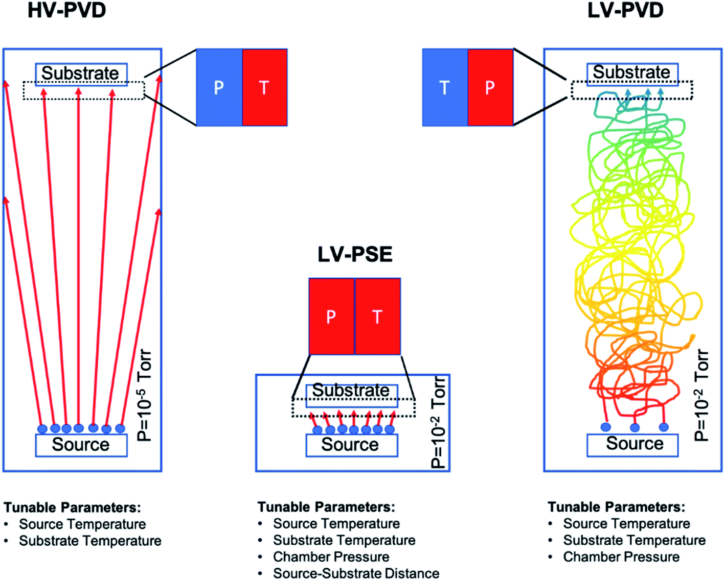 | ||
| Fig. 1 Schematic of three physical deposition methods. The HV-PVD applied in the current literature works at high vacuum (e.g. 10−5 torr) and with a long diffusion path such that in the substrate proximity low pressure and high temperature of the sublimated species are established. In contrast, our LV-PSE method is characterized by a low vacuum and short diffusion path that tailor high pressure and high temperature of the adatoms on the substrate side. This combination upsets the kinetic properties of the species impinging on the substrate with a major impact on the material quality and with a further effect on increasing the number of available operating (tunable) parameters. Finally, the right panel illustrates how moving from LV-PSE to LV-PVD (i.e. setting the source–substrate distance as in HV-PVD) implies a drastic reduction of the kinetic energy of the adatoms (temperature) at the substrate side that comes from the collisional path under low vacuum conditions and indeed makes unfeasible any deposition on a reasonable timescale. The pressure values are reported in torr according to most literature data. | ||
The LV-SPE method is indeed mid-way between conventional high-vacuum thermal evaporation25,30 and close-space-sublimation27 bearing some advantages from both sides. It operatively works as a sequential deposition of the inorganic layer (PbI2) followed by the evaporation of the organic moieties (MAI) that progressively infiltrate into it (Fig. 2a). No further thermal treatments are needed after deposition, and this represents an added-value to reduce processing times and costs. The mainstay resides in the substrate coaxially placed over the source at an optimized medium distance from the orifice of ∼2 cm (1–3 cm) that moves over each source on purpose. This short distance between the source and the substrate allows the molecules of the organic halide to arrive at the top of the PbI2 film with enough energy to start the conversion reaction. The conversion reaction would be unfeasible with the substrate positioned at the typical distance of HV-PVD (see Fig. 1). This short distance indeed enables the use of low vacuum conditions in the deposition chamber (i.e. ∼4 × 10⁻² mbar), which reduces the process complexity and costs. Moreover, with a proper implementation of the equipment, the chamber pressure easily becomes a process parameter to properly tailor, in synergy with the temperature of the source, the energy of the sublimated gas species. In the opposite direction, enlarging the source–substrate distances to tens of centimeters would cause collisional paths within the gas during travelling that hugely reduce the energy of the sublimated species before their arrival at the substrate surface, with even abundant material accumulation at the chamber walls. Collisions enormously reduce the deposition rate and increase contamination incorporation into the layer. Under high vacuum conditions and at high source–substrate distances as in HV-PVD (Fig. 1), instead, the gas molecules would retain their energy until their arrival at the substrate but with lower vapour pressure in proximity of the substrate due to geometrical effects (spread of the flux along long travels). As instead pointed out in ref Baekbo et al.,30 high MAI vapour pressure is mandatory to overcome the limitation of the low stitching coefficient.
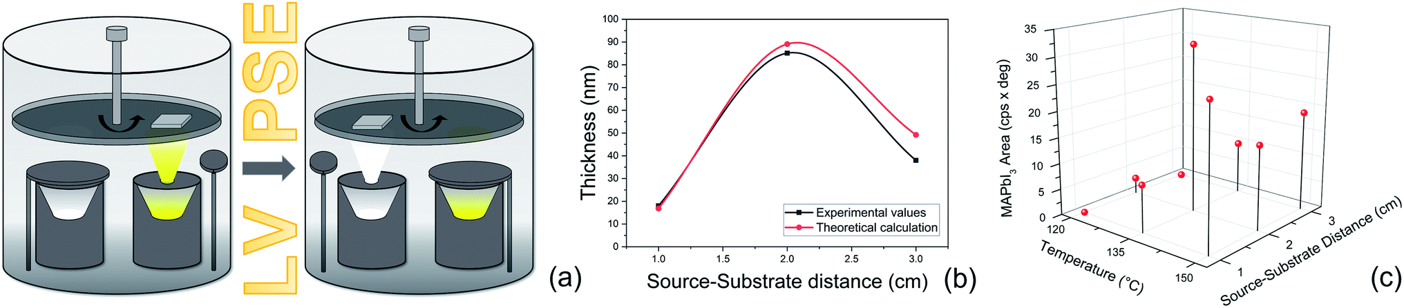 | ||
| Fig. 2 (a) Schematic representation of the low-vacuum deposition chamber for the two-step Low-Vacuum Proximity-Space-Effusion (LV-PSE) process used for the preparation of MAPbI3. (b) Comparison between the thickness of the PbI2 layer deposited in 30 minutes at different source–substrate distances and theoretical values obtained through the model. (c) Optimization of the MAI source temperature and source–substrate distance obtained by XRD analyses for the MAI deposition step. We reported the area of the peak at 2θ = 14.1° for all the combinations used. | ||
Therefore, with LV-PSE it is possible to use low vacuum conditions while retaining high gas molecule energy on the substrate, maintaining a good deposition rate and, at the same time, reducing loss of the sublimated species on the chamber sidewall. Hsiao et al.49 investigated the possibility to reduce the chamber pressure in HV-PVD. As a first observation, they investigated between 10−5 torr and 10−3 torr (our working range is around 1.5–3 × 10⁻² torr, i.e. 2–4 × 10⁻² mbar). Most importantly, they were not allowed to operate at high pressure (low vacuum) with their (standard) equipment according to the best efficiency value of 17.6% (Perovskite thickness 480 nm) achieved at a working pressure of 10−4 torr.
An evaluation of the LV-PSE process in terms of material growth is provided from the estimates of the mass transfer rate from the Knudsen cells and the substrate. The mass effusion rate from the cell's orifice can be calculated from the partial pressure of the molecular gas in the cell, which i.e. for the PbI2 case is reported in Kendler et al.50
 | (1) |
Assuming that quasi-ballistic transport conditions occur for the molecule transport from the cell's orifice to the substrate, an approximate estimate of the growth rate for PbI2 in the central position of the substrate (in a symmetric configuration) can be obtained from the balance between the deposition flux (jdep) and the evaporation flux (jev) using the formula reported by Avrov et al.51
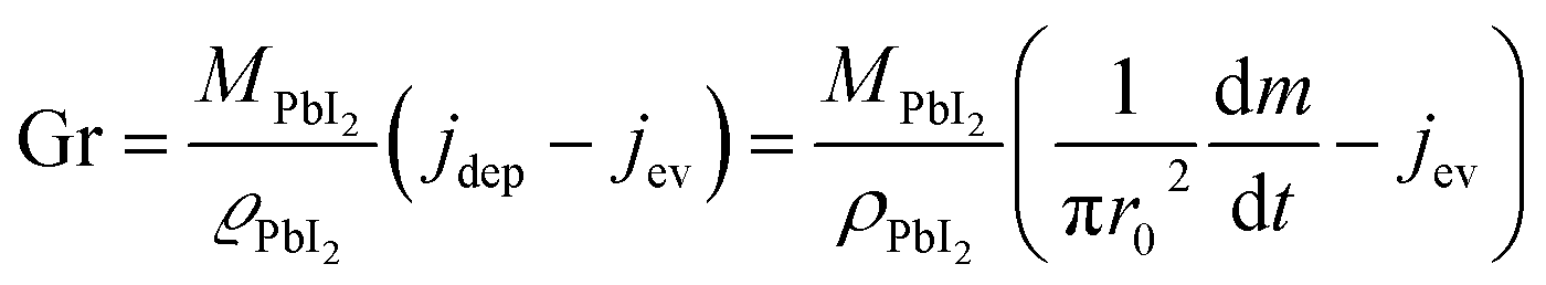 | (2) |
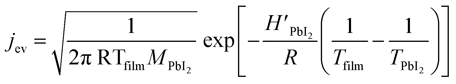 | (3) |
In Fig. 2b, a comparison between the PbI2 growth rate prediction, using the above equations, and the measured growth rate at three different distances between the cell and the substrate is shown. The substrate temperature values have also been measured using thermal indicator strips chosen in an appropriate range. The values are Tfilm = 150, 120, 100 °C for r0 = 1, 2 and 3 cm respectively. The chamber pressure is pchamb = 0.04 mbar. Both the model and the experimental data agree that the Knudsen cell's temperature at which deposition can be observed is T > 350 °C. Moreover, the experimental and theoretical optimal values for the growth rate are obtained for the couple parameters Tfilm 120 °C and r0 = 2 cm.
In this analysis, we use the literature Chickos et al.52 and Dualeh et al.53 and the derived values HPbI2 = 163.1 kJ mol−1 and TPbI2 = 646 K while 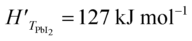 has been used for the evaporation/desorption flux. A lower value of the enthalpy constant (which can be considered a fitting parameter of the model) for the evaporation indicates that the competitive process with respect to the deposition involves the PbI2 molecules absorbed at the film surface which are on average less strongly bound with respect to the ones present in the materials loaded in the Knudsen cell.
With our optimized process conditions, the deposition rate for PbI2 is around 3 nm min−1 while about 60 minutes are needed to complete the conversion of PbI2 into MAPbI3 having a final desired thickness of 150 nm. The temperature for PbI2 sublimation was set at 350 °C. For the MAI deposition step, a temperature of 135 °C was used and the deposition time was optimized to reach the right stoichiometry and to avoid any presence of residual PbI2 on the sample. Immediately after the MAI deposition, the chamber is filled with N2 to avoid the decomposition of the MAPbI3 layer due to vacuum.16,54,55 The substrate temperature during the MAI deposition is 75 °C. That settles the best conditions for MAPbI3 formation. Accordingly, this temperature is given in the literature30,49 as the best one for MAPbI3 conversion via two-step deposition processes.
With this procedure, we deposited thin layers of MAPbI3 with thicknesses 150 nm and 80 nm, to demonstrate that a significant down-scaling is feasible with the LV-PSE method.
The optimization of the temperature of the crucible and source–substrate distance for the MAI deposition step is shown in Fig. 2c, where we plot the area of the XRD peak of the MAPbI3 peak at 2θ = 14.1° for all the combinations of the investigated temperatures and source–substrate distances. The best combination of parameters was 135 °C with a distance of 2 cm, which we consistently used for the preparation of the devices. In this case in fact, we obtained the highest area for the MAPbI3 peak and no peak was detected for PbI2. Even though a good result was also obtained using 150 °C at a distance of 1 cm, we decided to use the previous combination for the lower working temperature of the crucible, to longer preserve the MAI powder, and for a lower production energy consumption that is one of the main prerogatives of our technique. For the substrate temperature, we found, by means of direct temperature measurements, that the proximity between the source and substrate causes self-heating of the substrate that must be taken into account. The overall balance between self-heating and cooling provides a final temperature of 75 °C for the combination of temperature and distance of 135 °C and 2 cm. This is well known to be the convenient temperature for the MAI reaction.30,49
Fig. 3a shows the XRD patterns collected on 150 nm and 80 nm films deposited on ITO/PTAA substrates. In both samples we observe the diagnostic peaks related to MAPbI3 centered at 2θ = 14.1°, 28.4° and 35.2°. The lack of the peak at 12.67° related to PbI2 excludes the presence of residual PbI2 inside the films. Considering that the two samples have the same size, the intensities of corresponding peaks can be compared and suggest that the 150 nm-thick film has a high crystallographic quality.
 | ||
| Fig. 3 (a) Symmetric θ–2θ XRD patterns collected on MAPbI3 layers with different thicknesses deposited on ITO/PTAA. (b) Integrated XRD spatial analyses along the X-axis collected at fixed 2θ angles of 14.10° (red curve) and 12.67° (black curve) in a 2.5 cm × 2.5 cm MAPbI3 sample deposited on a glass substrate (c) XRD patterns collected on the deposited samples under different MAI time steps on ITO/PTAA substrates. In the inset, the XRD patterns of the as-deposited PbI2 sample and after an annealing test at 75 °C for 20 minutes. (d) Rocking curve collected at a fixed 2θ angle of 12.67° for the samples corresponding to different MAI deposition times on ITO/PTAA substrates. | ||
To explore the uniformity of the film over the deposited area, X-scan analyses were performed on a 2 cm × 2 cm sample made of a 150 nm-thick MAPbI3 layer deposited on a glass substrate. In the X-scan, the X-ray beam moves along X at fixed Bragg angles and has a size of 2 cm × 1 mm : indeed two angular values were used, namely 14.11° for MAPbI3 and 12.67° for PbI2 (Fig. 3b). We notice that the intensity of the curve related to MAPbI3 is uniform along X (box-like shape of the curve), while the intensity related to PbI2 is everywhere comparable with the noise, proving the compositional and thickness uniformity of the LV-PSE deposited MAPbI3 layer on 2 cm × 2 cm samples.
To study the MAPbI3 formation kinetics via LV-PSE, we have deposited 85 nm of PbI2 on ITO/PTAA and changed the duration of the second step of MAI evaporation. We used different progressively increasing deposition times, i.e. 20, 40 or 60 minutes, and correspondently we acquired the related diffraction patterns. In Fig. 3c, we interestingly observe that after 20 minutes of MAI deposition the peak of PbI2 at 12.7° has a higher intensity than in the starting sample (PbI2 only, t = 0). Since the PbI2 crucible is at room temperature during MAI deposition and indeed an addition of PbI2 is excluded, this finding suggests that the initial molecular infiltration of methylammonium iodide inside the layer of PbI2, with the related kinetics, improves the lattice order of the hosting material during the formation of the starting perovskite nuclei. To understand this phenomenon, we have added a post-deposition annealing step at 75 °C for 20 minutes in situ during XRD analysis to be confident that this rearrangement of the PbI2 film is not simply caused by temperature. The test did not produce any increase of the PbI2 peak intensity as we would expect due to the crystallization of an eventual amorphous phase in the film after an annealing step. For further evaluation, we have additionally performed on the same sample an annealing at 150 °C for 1 h. In Fig. S1† the XRD patterns collected before and after the annealing do not show any significant increase of the peak intensity confirming that the layer is fully crystallized just after deposition. We have also performed X-ray Photoelectron Spectroscopy (XPS) analyses on the as-deposited PbI2 film to measure the atomic ratio between lead and iodine and to have information about the species inside the film (Fig. S3†). Fig. S3a† shows the Pb4f spectral region with a typical lead doublet. After the deconvolution of the peaks, no sign of metallic lead is found but rather a doublet peak is detected with components centered at 138.60 eV (Pb4f7/2) and 143.46 eV (Pb4f5/2), typical of lead halide compounds. The absence of any Pb0 is confirmed also by the quantitative analyses, where a Pb/I ratio of 0.51 very close to the expected value is measured. We have acquired XPS spectra also after the 60 minutes of MAI deposition. The Pb/I ratio in this case is 0.35 and is also very close to the expected value of 0.33. In this case the Pb components are shifted to 136.20 eV (Pb4f7/2) and 141.06 eV (Pb4f5/2) due to the proximity of MA+ cations.
To further investigate the observed rearrangement of the PbI2 film during MAI deposition, rocking curves (rc) corresponding to the diagnostic peak at 12.67° were acquired. All the peaks reported in Fig. 3c denote a texturing of the PbI2 layers along the [0001] direction. According to this, the rc peaks in Fig. 3d show that the highest degree of preferential orientation is promoted after 20 minutes of MAI deposition. After this first reorganization of the film, the peak intensity starts decreasing due to the conversion of PbI2 into MAPbI3. At the end of the process, we do not see PbI2 left inside the film, thus confirming the complete material conversion.
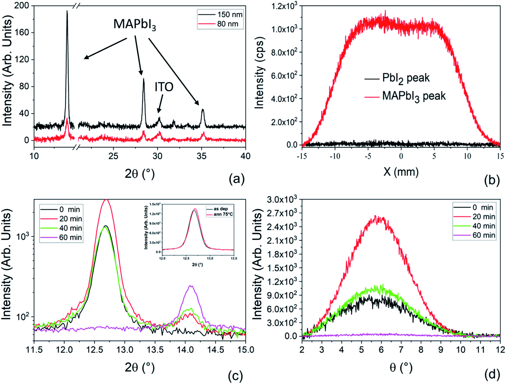
To gain atomistic insights into the early mechanism of MAI diffusion within the PbI2 lattice and their reaction, we performed DFT calculations, simulating the consecutive intercalation of MA+/I− complexes at the PbI2 layers. Fig. 4a shows the initial layered configuration of the PbI2 crystal, where Pb atoms are aligned at the center of each layer, whereas I atoms are exposed at the layer surfaces. The initial diffusion of MAI molecular structures [Fig. 3b and c] spontaneously triggers a reaction with the PbI2 material, as the MA+ cations interact through hydrogen bonding with the I atoms of the PbI2 crystal. As a result, this interaction weakens the PbI2 bonds for Pb/I atoms that are adjacent to the MA+ cations and favors the formation of novel Pb–I bonds between those Pb atoms and the iodide derived from the MAI vapor. This process takes place through the displacement of the Pb atoms towards the interlayer area and consequently creates Pb voids within the PbI2 layer. The Pb atoms that bind with the I atoms of the iodide vapor lose momentarily their octahedral coordination and acquire a 4-fold coordination, approaching the Pb4+ oxidation state. This condition is highly metastable, as the intercalation of further MA+/I− complexes gives rise to the construction of novel PbI6 octahedra in the interlayer region (restoring the stable Pb2+ character of lead in iodide structures) and gradually transforms the two-dimensional PbI2 layers into a three-dimensional structure [Fig. 3d and e]. We expect that the kinetics of this process continue until the full transformation of the PbI2 material into MAPbI3.
 | ||
| Fig. 4 DFT calculations of MAI intercalation within PbI2 layers. (a) Ideal PbI2 structure and intercalation of (b) 1 MAI molecule, (c) 2 MAI molecules, (d) 3 MAI molecules and (e) 4 MAI molecules within the layers of the PbI2 structure. | ||
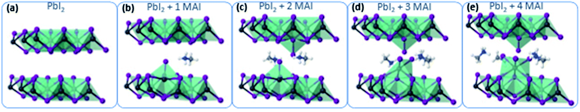
To deeply understand the time-dependent mechanism of MAI molecules incorporation into the PbI2 pristine film, we have performed XRD analyses using grazing incidence geometries for all the samples prepared at various MAI step times. With this configuration, using different incidence angles, we can discriminate the mutual position of PbI2 and MAPbI3 along the thickness of the film. In fact, lower is the incidence angle shallower is the portion of the layer contributing to the signal. As can be seen in Fig. 6a, the peak intensity at 2θ = 12.67° is higher for higher incidence angles; according to that at 0.3° and 0.4° we are not able to investigate all the thicknesses. In contrast at 0.5° we investigate the entire film thickness.
We want to point out that the XRD data reported in Fig. 5 were acquired on the same samples reported in Fig. 3a and c but using a different acquisition geometry (grazing incidence configuration). Under grazing incidence, that is specifically useful for depth resolved analyses, the randomly oriented component of the films is detected whilst in symmetric θ–2θ geometry (Fig. 3) the oriented (textured) part of the films primarily contributes. Since it is demonstrated (polar Fig. in S2† and 3c) that the PbI2 layer is highly textured, the random component is not as intense as the majority component taken in the symmetric geometry. It is detected at relatively high incidence suggesting its location mostly at the bottom interface. On the other hand, as soon as the whole PbI2 layer is converted to MAPbI3 (Fig. 5d), no PbI2 contribution is found whatever the incidence angle used.
 | ||
| Fig. 5 (a) XRD patterns collected in grazing incidence configuration at three different incidence angles, namely 0.3°, 0.4° and 0.5° for the PbI2 deposited sample, (b) after 20 minutes, (c) 40 minutes and (d) 60 minutes of MAI deposition on ITO/PTAA substrates. (e) Schematic representation of the conversion mechanism from PbI2 to MAPbI3 during the MAI deposition step. In the pristine sample only the PbI2 peak is detected at 2θ = 12.67°. Along the MAI deposition step, the conversion of PbI2 to MAPbI3 starts from the topmost part of the film toward the bottom until the complete conversion has occurred. | ||
The same behavior has occurred for all samples with variation in the PbI2 intensity which are more pronounced in the sample after 20 minutes of MAI deposition at different scanning angles (see Fig. 5b). Hereinafter, the PbI2 peak intensity decreases with increasing MAI deposition time due to the consumption of PbI2 during the formation of the perovskite. In contrast, the peaks at 2θ = 14.1° related to the MAPbI3 film have the same intensity for the three incidence angles after the 20 minutes of MAI deposition. In this case, we mostly investigate the upper portion of the layer suggesting that the first conversion of PbI2 to MAPbI3 occurs at the top of the deposited PbI2 film. After 40 minutes of MAI deposition, only the 0.3° incidence angle pattern shows a slightly lower intensity for the MAPbI3 peak with respect to the 0.4° and 0.5° incidence angles. At 0.3°, we are not able to collect the signal from all the already converted MAPbI3 thicknesses, suggesting the increase of the PbI2 conversion to MAPbI3 (Fig. 5c). Finally, in the sample after 60 minutes of MAI deposition (Fig. 5d), the signal related to the residual PbI2 is not visible meaning that all the PbI2 is converted into MAPbI3 according with the lack of the PbI2 peak shown in Fig. 3a. We additionally notice that the intensity of the MAPbI3 peak at 2θ = 14.1° in Fig. 5d increases with increasing the incidence angle according to the progressively higher beam penetration depth. Based on our findings, we conclude that the conversion of the PbI2 film to MAPbI3 starts from the topmost layer of PbI2 progressively towards the lowermost part until the whole film is fully converted into MAPbI3 as presented in Fig. 5e. This description agrees with previously reported studies on PbI2 conversion via gas-phase MAI deposition,56,57 thus listing the LV-PSE method as a solid-state reaction piloted by MAI diffusion.
3.2 Morphological analyses
The process optimization done on the 150 nm thick MAPbI3 layer has suggested a viable path for the downscaling of the perovskite layer thickness. On this basis, uniform and fully reacted layers that are only 80 nm thick have been deposited by LV-PSE. The analyses of the morphology and of the optical properties of this very thin layer compared to the 150 nm-thick MAPbI3 film are hereafter discussed in detail.Field emission scanning electron microscope (FE-SEM) analyses shown in Fig. 6 reveal a peculiar change in the morphologies of the films deposited during the LV-PSE processes. In Fig. 7a are shown the images acquired after 15 minutes of PbI2 deposition on an ITO/PTAA substrate used as a template (first step) to grow the 80 nm thick MAPbI3 film. The film is composed of randomly oriented PbI2 small (around 100 nm) platelet-shaped grains. We have also performed chemical analyses on the 30 minutes deposited PbI2 layer by Energy Dispersive X-ray (EDX) spectroscopy to check the composition (Fig. S4†). The Pb/I ratio from EDX was 0.49 in good agreement with the expected value. The resulting MAPbI3 film, after 30 minutes of MAI deposition, is compact with a grain size of around 100 nm. Most importantly, pinholes are not visible on the surface (Fig. 6b). According to what is found in the thinner layer, the PbI2 film deposited after 30 minutes (Fig. 6c) is also composed of platelets but with a bigger size (200 nm). The comparison between the two samples demonstrates that the platelets continue to grow by proceeding PbI2 deposition. The PbI2 platelets are the template for the reacting MAPbI3 film. As a matter of fact, the morphology of MAPbI3 is modelled on the PbI2 platelet size, with the final grain size similar to that of the templating layers in both samples (Fig. 6b and d). The incorporation of MAI into the PbI2 platelets allows them to fill the empty space between the platelets due to the increase of cell volume during the conversion of PbI2 to MAPbI3. The technologically interesting finding that such thin layers are totally compact without pinholes, in full agreement with XRD analysis by the X-scans, paves the way for very down-scaled PSCs.
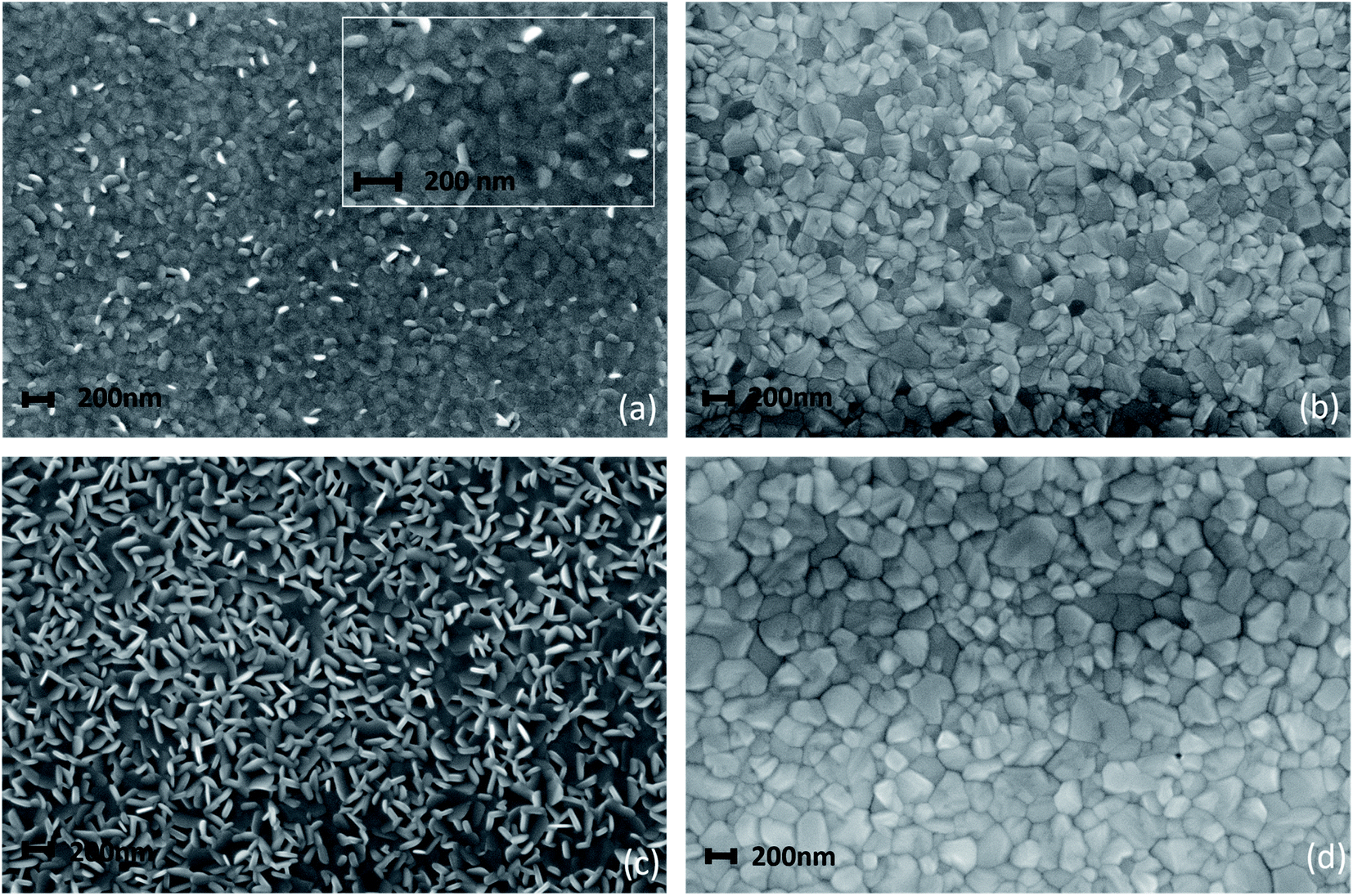 | ||
| Fig. 6 SEM images collected on (a) PbI2 deposited on an ITO/PTAA substrate using a deposition time of 15 minutes and (b) the converted MAPbI3 after 30 minutes of MAI deposition. (c) PbI2 deposited for 30 minutes and (d) the resultant MAPbI3 after 60 minutes of MAI deposition. | ||
 | ||
| Fig. 7 (a) Transmittances of 150 nm and 80 nm MAPbI3 films. (b) The refractive index n (dashed line) and the extinction coefficient k (solid line) of 150 nm and 80 nm MAPbI3 films. Note the pre-gap tail that is close to ideality in the 150 nm-thick layer. (c) Absorption coefficient (nm−1) and absorption depth (nm) of 150 nm-thick MAPbI3 layers. | ||
3.3 Optical properties
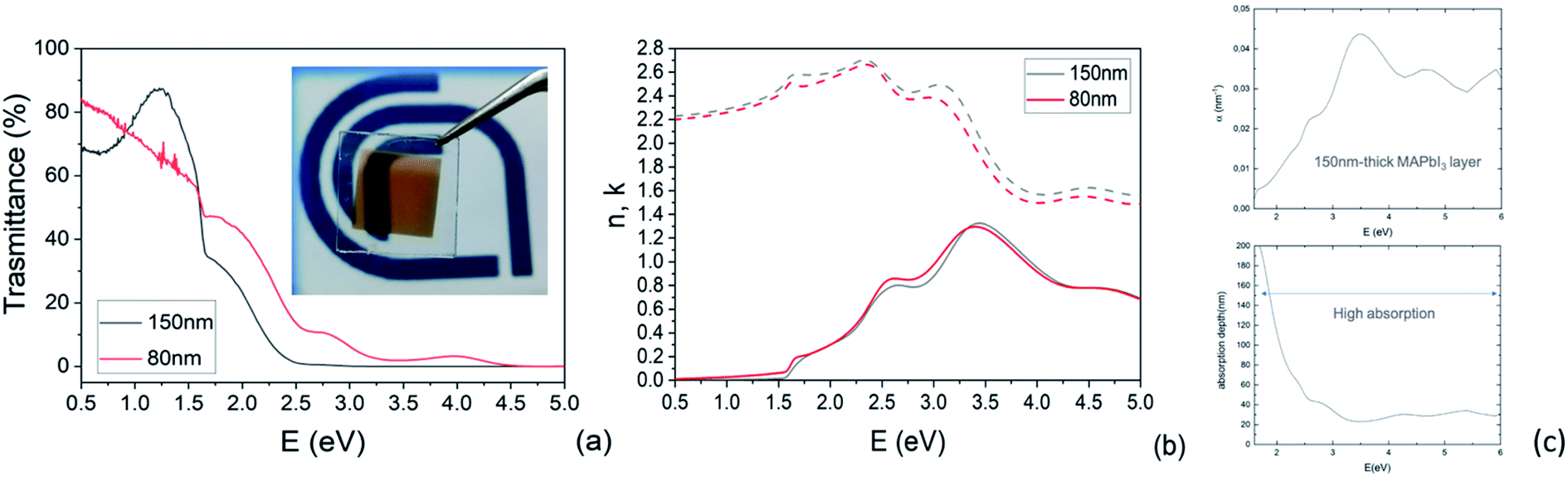
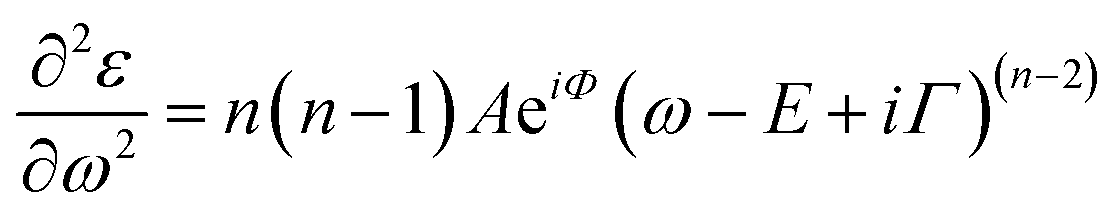
Transmittance spectra collected on both thick and thin samples deposited on ITO/PTAA substrates show the typical optical features of MAPbI3 films (Fig. 7a) with an abrupt decrease below the gap (810 nm). The sample was kept in a closed chamber with an overpressure of N2 to prevent degradation. The thickness of the perovskite layer (80 nm and 150 nm) was determined by verifying that n obeys the Cauchy equation in the transparent infrared region. The average visible transmittance calculated for 150 nm and 80 nm samples in the range 400–800 nm was 20% and 32.8% respectively. Reducing the thickness of the active layer to 80 nm thus increases the transmittance in the visible range.In Fig. 7b, we show the refractive index n and the extinction coefficient k, strictly related to the absorption coefficient of the material, as extracted by Spectroscopic Ellipsometry (SE) measurements for the two PSK layers. The thickness of the perovskite layer (80 nm and 150 nm) was determined by verifying that n obeys the Cauchy equation in the transparent infrared region. The measurements were done on glass substrates to exclusively probe the absorbing layer. The sample was kept in a closed chamber with an overpressure of N2 to prevent degradation. Interband transition have been identified by applying critical point analysis.58–60 Critical point (CP) analysis is based on the simultaneous fit of the second derivatives of the real and imaginary parts of the dielectric function (ε) with a function like (one for each CP):
 | (4) |
| E g (eV) | E 1 (eV) | E 2 (eV) | E 3 (eV) | |
|---|---|---|---|---|
| THIN | 1.612 ± 0.001 | 2.505 ± 0.003 | 3.21 ± 0.01 | 4.52 ± 0.06 |
| THICK | 1.605 ± 0.001 | 2.423 ± 0.008 | 3.28 ± 0.02 | 4.27 ± 0.18 |
In Fig. S5† are reported the ellipsometric experimental data (Psi and Delta) collected at various angles and the Cauchy fit. In addition to this, the absorption coefficient was measured by spectroscopic ellipsometry and converted into the absorption depth as a function of the incident photon energy as shown in Fig. 7c for the 150 nm-thick layer. The combination of the two parameters highlights that, even in a relatively thin layer, the absorption capability is still high above the bandgap. As a matter of fact, ∼60% of incident photons with energy above 2 eV are absorbed within the first 20–100 nm in the MAPbI3 layer. Photons with energy in the range of 1.5–2 eV are absorbed within 100–200 nm with indeed only a partial loss of absorption that, on the other hand, guarantees the semitransparency of the layer without excessively penalizing the device performances.
In order to further explore the material quality in its optical response, we recorded the steady state photoluminescence, measured its quantum yield (PLQY) and analyzed the PL decay (TRPL) of the as-deposited pristine isolated 150 nm MAPbI3 films deposited on glass substrates (Fig. 8). The PLQY determined on a non-quenching substrate is used to estimate the maximum value of the material-specific luminescence yield. This quantity is a direct measure of the optoelectronic quality of the absorber material, as a low emission yield means high additional non-radiative recombination, which would not allow for high Voc.61,62 The PLQY, in turn, strongly depends upon the excitation fluence, as the electronic defects in the material would be more severely impacting upon reduced density of carriers (low excitation fluences) while high fluences would, in turn, lead to higher PLQY.
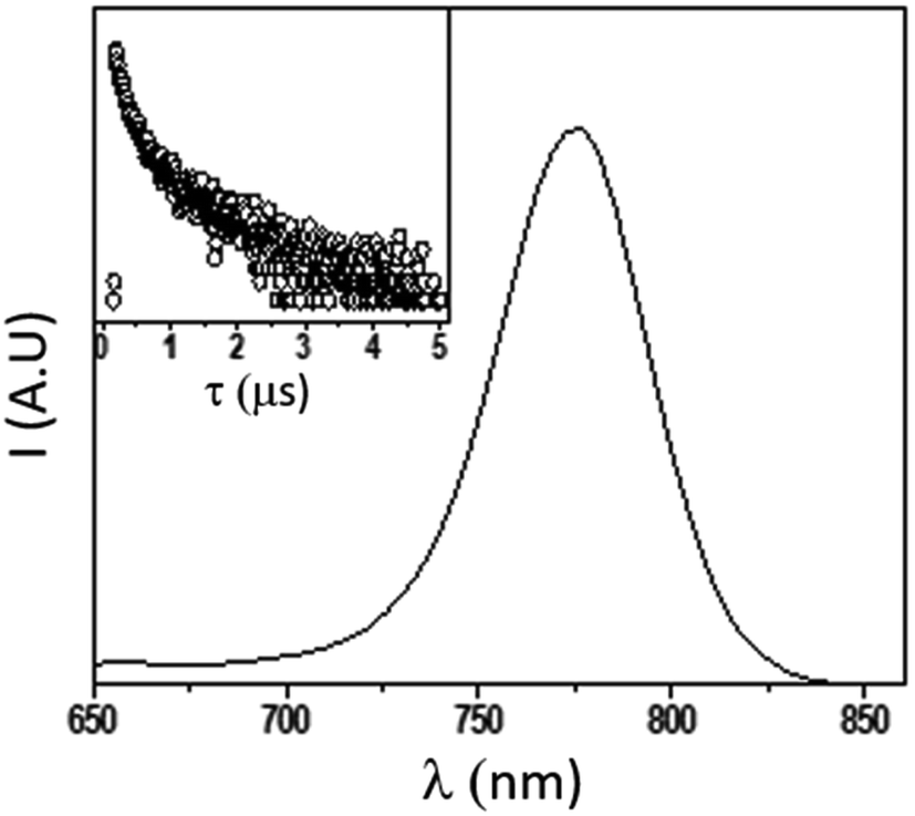 | ||
| Fig. 8 Emission spectrum (main, exc = 405 nm) and corresponding lifetime decay (inset, exc = 405 nm; em: 750 nm) of MAPbI3 thin film on glass. | ||
At very low excitation fluence (<1.0 mW cm−2), only a few reports on MAPbI3 show PLQY around 1% and those are associated with post-treated samples or chloride including samples;63 here we record a 0.9% PLQY using 0.6 mW cm−2 power density, implying an optimal thin film for photovoltaic exploitation. Additional evidence of this claim is given by time resolved PL analyses, which show long living free carriers. In line with what is usually observed for hybrid organic–inorganic perovskites, we found a complex exponential decay (in this case a biexponential function best fits the decay), since there is no clear consensus on how to exactly assign the various components to a given TRPL curve, we used a weighted average of the diverse decay components:
 | (5) |
obtaining a value of 234 ns.63 This is a very long radiative decay for pristine MAPbI3 (ref. 63) considering that lifetimes in the order of μs have been observed only when chloride-containing species were added to the precursor's solutions, with a beneficial role played by these species in the growth of large crystallites. These results imply that LV-PSE is an optimal technique for the deposition of thin, performing, Perovskite layers.
3.4 Electrical properties
In light of all our findings, the two MAPbI3 thin layers have been implemented in p–i–n PSC architectures and tested. The efficiency values recorded on the two set of PSCs as a function of the MAPbI3 thickness highlight outstanding performances not yet reported in the literature for such thin layers. In addition, it is worth noting that there is a complete lack of hysteresis during forward and reverse scans as shown in Fig. 9, due to the use of the organic ETL and HTL materials but also ascribed to the high quality of the perovskite film64–66 according to PL and SE analyses.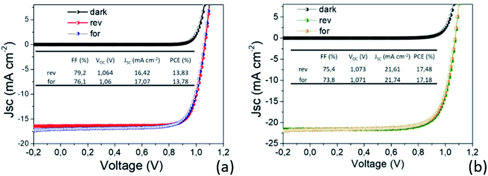 | ||
| Fig. 9 I–V characterization of the best prepared devices with (a) 80 nm and (b) 150 nm MAPbI3 active layers. The AVT moves from 32.8% to 20%. | ||
Fig. 10 shows the distribution of photovoltaic parameters displayed as boxplots for 16 cells fabricated with 80 nm (8 cells) and 150 nm (8 cells) MAPbI3 layers. The average value of power conversion efficiency (PCE) for the two sets of devices is 12.9% and 14.4%, respectively. The best fabricated device exhibits a 17.48% efficiency (MAPbI3 150 nm-thick) that stabilizes at 16.5% upon light soaking (Fig. S6†). The record for 80 nm-thick layers instead is 13.8%, with a narrow distribution of the other measured values. These results place our devices among the best semitransparent devices based on MAPbI3 (ref. 67 and 68) and further show how this deposition protocol represents important progress in the field.
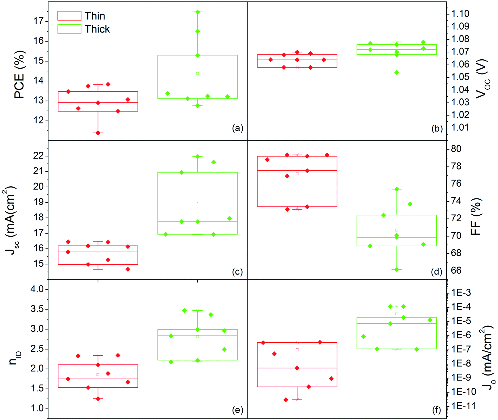 | ||
| Fig. 10 Box plot of (a) efficiency (PCE), (b) open circuit voltage (Voc), (c) short circuit current (Jsc), (d) fill factor (FF), (e) ideality factor (niD) and (f) reverse saturation current (J0) from the electrical characterization of all the prepared devices with 80 nm thick and 150 nm thick MAPbI3 active layers. | ||
Small differences in the open circuit voltage (Voc) values, in the range 1.05–1.08 V (Fig. 10b), are found between the two families of devices, whilst the short circuit current (Jsc) is definitely higher in the thicker devices (Fig. 10c). The Fill Factor (FF) has instead a countertrend with the device thickness (77% vs. 71%) that can account for different shunt or series resistances (Fig. 10d). To provide some insights into that, we additionally provide the statistical distributions of the ideality factor (nID) and reverse saturation current (J0) in Fig. 10e and f respectively, calculated according to ref. 69 using eqn (S1) and (S2).† The ideality factor was also differently calculated following Tress et al.70 using the J–V curve taken under dark conditions with results confirming the gap vs. MAPbI3 thickness.
The lower values of nID in thin devices can indicate a better heterojunction quality.70 The relationship is not necessarily straightforward,70,71 but, in this respect, we additionally notice that low nID corresponds to low J0. This statistical evidence, complemented with the higher FF, indeed denotes lower non-radiative recombination in the thin PSC likely associated with less pronounced interfacial trapping.72,73 The thickness halving without proportionally reducing the efficiency satisfies the technological requirements for transparent PSCs, and represents a unique example in the current panorama of similar deposition methods.24,36
4. Conclusions
We described a newly designed two-step vacuum deposition process called LV-PSE to prepare high quality MAPbI3. The process benefits from the low vacuum conditions (∼2–4 × 10⁻² mbar) and the short diffusion path (∼2 cm) of the sublimated species that provide them with high pressure and high temperature at the substrate side. This unique configuration allows controlling the rate of mass exchange at the vapor-substrate interface for a fine tuning of the material quality.We disclose that the conversion of the PbI2 film to MAPbI3 starts from the top surface of the film to the bulk via an adsorption–incorporation–migration mechanism guided by the gradient of energetic MAI concentration. The final MAPbI3 layer is composed of grains with a diameter from 50 to 200 nm. The film is compact and without pinholes which makes the perovskite suitable for photovoltaic applications. PL analyses, according to SE, showed that the active layer has a very low tail of electronically active defects, and indeed, on this basis, we were able to build up efficient solar cells with a p–i–n architecture. With just 80 nm-thick active layers, we achieved a mean efficiency value of 12.9% and best value of 13.8% with an AVT value of 32.8% which makes these devices unique in the current panorama of MAPbI3 materials prepared with different methods and suitable for the application in BIPV. Using 150 nm-thick films, we were able to achieve 14.4% mean efficiency and a best stabilized efficiency value of 16.5% with no hysteresis ascribed to the low density of defects inside the layer and at the interfaces coupled with an organic ETL and HTL. To our knowledge, this value represents the highest efficiency published on p–i–n architectures for similar scaled thicknesses.
The use of LV-PSE and the scaled MAPbI3 thicknesses, associated with excellent efficiency values, paves the way for an affordable cost reduction for device fabrication besides allowing a reduction by ∼1/3 of the Pb content inside the devices against environmental concerns.
Conflicts of interest
There are no conflicts to declare.Acknowledgements
The authors gratefully acknowledge the project Best4U-“Tecnologia per celle solari bifacciali ad alta Efficienza a 4 terminali per utility scale” founded by the Italian Ministry of University and Scientific Research (MIUR), Bando PON R&I 2014–2020 e FSC “Avviso per la presentazione di Progetti di Ricerca Industriale e Sviluppo Sperimentale nelle 12 aree di Specializzazione individuate dal PNR 2015–2020”-decreto concessione agevolazione protocollo 991 del 21 maggio 2019 MIUR (contract number: PON ARS01_00519; CUP B88D19000160005). We would like to acknowledge the Kenosistec s.r.l. technical office for the realization of the customized LP-PSE equipment and the support. In particular, we would like to thank Stefano Perugini (Technical Manager), Giovanni Barbieri (Electrical Project), Michele Abbiati and Michele Garavaglia (Mechanical Project) and Simone Colucci (Testing). We would like to thank Guglielmo Guido Condorelli (Department of Chemistry of University of Catania) for his contribution on XPS analyses.References
- J. Burschka, N. Pellet, S.-J. Moon, R. Humphry-Baker, P. Gao, M. K. Nazeeruddin and M. Grätzel, Nature, 2013, 499, 316–319 CrossRef CAS PubMed.
- N. J. Jeon, J. H. Noh, W. S. Yang, Y. C. Kim, S. Ryu, J. Seo and S. Il Seok, Nature, 2015, 517, 476–480 CrossRef CAS PubMed.
- A. K. Jena, A. Kulkarni and T. Miyasaka, Chem. Rev., 2019, 119, 3036–3103 CrossRef CAS PubMed.
- W. Huang, J. S. Manser, P. V. Kamat and S. Ptasinska, Chem. Mater., 2016, 28(1), 303–311 CrossRef CAS.
- M. Zhang, F. Yuan, W. Zhao, B. Jiao, C. Ran, W. Zhang and Z. Wu, Org. Electron., 2018, 60, 57–63 CrossRef CAS.
- V. Adinolfi, W. Peng, G. Walters, O. M. Bakr and E. H. Sargent, Adv. Mater., 2018, 30, 1–13 CrossRef PubMed.
- J. Zhou and J. Huang, Adv. Sci., 2018, 5, 1700256 CrossRef PubMed.
- N. Patel, S. Dias and S. B. Krupanidhi, J. Electron. Mater., 2018, 47, 2306–2315 CrossRef CAS.
- H. W. Chen, N. Sakai, A. K. Jena, Y. Sanehira, M. Ikegami, K.-C. Ho and T. Miyasaka, J. Phys. Chem. Lett., 2015, 6, 1773–1779 CrossRef CAS PubMed.
- S. D. Stranks, G. E. Eperon, G. Grancini, C. Menelaou, M. J. P. Alcocer, T. Leijtens, L. M. Herz, A. Petrozza and H. J. Snaith, Science, 2013, 342, 341–344 CrossRef CAS PubMed.
- https://www.nrel.gov/pv/assets/pdfs/best-research-cell-efficiencies.20201228.pdf .
- A. Kojima, K. Teshima, Y. Shirai and T. Miyasaka, J. Am. Chem. Soc., 2009, 131, 6050–6051 CrossRef CAS PubMed.
- Y. Zhao and K. Zhu, J. Phys. Chem. Lett., 2014, 5, 4175–4186 CrossRef CAS PubMed.
- W. S. Yang, J. H. Noh, N. J. Jeon, Y. C. Kim, S. Ryu, J. Seo and S. Il Seok, Science, 2015, 348, 1234–1237 CrossRef CAS PubMed.
- A. Ng, Z. Ren, Q. Shen, S. H. Cheung, H. C. Gokkaya, S. K. So, A. B. Djurišić, Y. Wan, X. Wu and C. Surya, ACS Appl. Mater. Interfaces, 2016, 8, 32805–32814 CrossRef CAS PubMed.
- E. Smecca, Y. Numata, I. Deretzis, G. Pellegrino, S. Boninelli, T. Miyasaka, A. La Magna and A. Alberti, Phys. Chem. Chem. Phys., 2016, 18, 13413–13422 RSC.
- I. Deretzis, E. Smecca, G. Mannino, A. La Magna, T. Miyasaka and A. Alberti, J. Phys. Chem. Lett., 2018, 9, 3000–3007 CrossRef CAS PubMed.
- A. Alberti, I. Deretzis, G. Mannino, E. Smecca, F. Giannazzo, A. Listorti, S. Colella, S. Masi and A. La Magna, Adv. Energy Mater., 2019, 9, 1803450 CrossRef.
- A. J. Knight and L. M. Herz, Energy Environ. Sci., 2020, 13, 202 RSC.
- I. Deretzis, A. Alberti, G. Pellegrino, E. Smecca, F. Giannazzo, N. Sakai, T. Miyasaka and A. La Magna, Appl. Phys. Lett., 2015, 106, 131904 CrossRef.
- M. Liu, M. B. Johnston and H. J. Snaith, Nature, 2013, 501, 395–398 CrossRef CAS PubMed.
- W. A. Dunlap-Shohl, E. T. Barraza, A. Barrette, K. Gundogdu, A. D. Stiff-Roberts and D. B. Mitzi, ACS Energy Lett., 2018, 3(2), 270–275 CrossRef CAS.
- N. J. Jeon, J. H. Noh, W. S. Yang, Y. C. Kim, S. Ryu, J. Seo and S. Il Seok, Nature, 2015, 517, 476–480 CrossRef CAS PubMed.
- B. Danekamp, N. Droseros, F. Palazon, M. Sessolo, N. Banerji and H. J. Bolink, ACS Appl. Mater. Interfaces, 2018, 10, 36187–36193 CrossRef CAS PubMed.
- D. Perez-del-Rey, P. P. Boix, M. Sessolo, A. Hadipour and H. J. Bolink, J. Phys. Chem. Lett., 2018, 9, 1041 CrossRef CAS PubMed.
- V. Arivazhagan, J. Xie, Z. Yang, P. Hang, M. M. Parvathi, K. Xiao, C. Cui, D. Yang and X. Yu, Sol. Energy, 2019, 181, 339–344 CrossRef CAS.
- Q. Guo, C. Li, W. Qiao, S. Ma, F. Wang, B. Zhang, L. Hu, S. Dai and Z. Tan, Energy Environ. Sci., 2016, 9, 1486 RSC.
- L. Gu, S. Wang, X. Fang, D. Liu, Y. Xu, N. Yuan and J. Ding, ACS Appl. Mater. Interfaces, 2020, 12, 33870–33878 CrossRef CAS PubMed.
- A. Ng, Z. Ren, Q. Shen, S. H. Cheung, H. C. Gokkaya, G. Bai, J. Wang, L. Yang, S. K. So, A. B. Djurišić, W. W. Leung, J. Hao, W. K. Chan and C. Surya, J. Mater. Chem. A, 2015, 3, 9223–9231 RSC.
- M. J. Baekbo, O. Hansen, I. Chorkendorff and P. C. K. Vesborg, RSC Adv., 2018, 8, 29899 RSC.
- Z. Zhou, Z. Qiang, T. Sakamaki, I. Takei, R. Shang and E. Nakamura, ACS Appl. Mater. Interfaces, 2019, 11, 22603–22611 CrossRef CAS PubMed.
- A. Cannavale, P. Cossari, G. E. Eperon, S. Colella, F. Fiorito, G. Gigli, H. J. Snaith and A. Listorti, Energy Environ. Sci., 2016, 9, 2682–2719 RSC.
- C. Roldan-Carmona, O. Malinkiewicz, R. Betancur, G. Longo, C. Momblona, F. Jaramillo, L. Camacho and H. J. Bolink, Energy Environ. Sci., 2014, 7, 2968–2973 RSC.
- J. H. Lee, J. H. Heo, S. H. Im and O. O. Park, ACS Appl. Mater. Interfaces, 2020, 12(9), 10527–10534 CrossRef PubMed.
- G. E. Eperon, V. M. Burlakov, A. Goriely and H. J. Snaith, ACS Nano, 2014, 8, 591–598 CrossRef CAS PubMed.
- H. Wang, H. A. Dewi, T. M. Koh, A. Bruno, S. Mhaisalkar and N. Mathews, ACS Appl. Mater. Interfaces, 2020, 12, 484–493 CrossRef CAS PubMed.
- C.-Y. Chang, K.-T. Lee, W.-K. Huang, H.-Y. Siao and Y.-C. Chang, Chem. Mater., 2015, 27, 7119 CrossRef CAS.
- J. H. Heo, H. J. Han, M. Lee, M. Song, D. H. Kim and S. H. Im, Energy Environ. Sci., 2015, 8, 2922–2927 RSC.
- Z. Li, Y. Zhao, X. Wang, Y. Sun, Z. Zhao, Y. Li, H. Zhou and Q. Chen, Joule, 2018, 2, 1559–1572 CrossRef CAS.
- H. Shen, T. Duong, J. Peng, D. Jacobs, N. Wu, J. Gong, Y. Wu, S. K. Karuturi, X. Fu, K. Weber, X. Xiao, T. P. White and K. Catchpole, Energy Environ. Sci., 2018, 11, 394 RSC.
- J. Xu, C. C. Boyd, Z. J. Yu, A. F. Palmstrom, D. J. Witter, B. W. Larson, R. M. France, J. Werner, S. P. Harvey, E. J. Wolf, W. Weigand, S. Manzoor, M. F. A. M. van Hest, J. J. Berry, J. M. Luther, Z. C. Holman and M. D. McGehee, Science, 2020, 367, 1097–1104 CrossRef CAS PubMed.
- L. K. Ono, S. Wang, Y. Kato, S. R. Raga and Y. Qi, Energy Environ. Sci., 2014, 7, 3989 RSC.
- A. Alberti, E. Smecca, A. La Magna, S. Perugini and M. Abbiati, Metodo ed apparato per la deposizione di uno strato di perovskite su un substrato, Italian patent application no. 102021000001898, 29/01/2021 Search PubMed.
- S. Masi, F. Aiello, A. Listorti, F. Balzano, D. Altamura, C. Giannini, R. Caliandro, G. Uccello-Barretta, A. Rizzo and S. Colella, Chem. Sci., 2018, 9, 3200–3208 RSC.
- P. Giannozzi, S. Baroni, N. Bonini, M. Calandra, R. Car, C. Cavazzoni, D. Ceresoli, G. L. Chiarotti, M. Cococcioni and I. Dabo, et al. , J. Phys.: Condens. Matter, 2009, 21, 395502 CrossRef PubMed.
- J. P. Perdew, K. Burke and M. Ernzerhof, Phys. Rev. Lett., 1996, 77, 3865 CrossRef CAS PubMed.
- D. Vanderbilt, Phys. Rev. B: Condens. Matter Mater. Phys., 1990, 41, 7892 CrossRef PubMed.
- H. J. Monkhorst and J. D. Pack, Phys. Rev. B: Solid State, 1976, 13, 5188 CrossRef.
- S. Hsiao, H. Lin, W. Lee, W. Tsai, K. Chiang, W. Liao, C. Ren-Wu, C. Chen and H. Lin, Adv. Mater., 2016, 28, 7013–7019 CrossRef CAS PubMed.
- R. Kendler, F. Dreisbach, R. Seif, S. Pollak and M. Petermann, Rev. Sci. Instrum., 2019, 90, 055105 CrossRef PubMed.
- D. D. Avrov, A. S. Bakin, S. I. Dorozhkin, V. P. Rastegaev and Y. M. Tairov, J. Cryst. Growth, 1999, 198–199 Search PubMed.
- J. S. Chickos and W. E. Acree Jr, J. Phys. Chem. Ref. Data, 2002, 31, 537–698 CrossRef CAS.
- A. Dualeh, P. Gao, S. Il Seok, M. K. Nazeeruddin and M. Gratzel, Chem. Mater., 2014, 26, 6160–6164 CrossRef CAS.
- A. Alberti, I. Deretzis, G. Pellegrino, C. Bongiorno, E. Smecca, G. Mannino, F. Giannazzo, G. G. Condorelli, N. Sakai, T. Miyasaka, C. Spinella and A. La Magna, ChemPhysChem, 2015, 16, 3064 CrossRef CAS PubMed.
- A. Alberti, E. Smecca, S. Sanzaro, G. Mannino, I. Deretzis and A. La Magna, Riv. Nuovo Cimento Soc. Ital. Fis., 2019, 42, 301–366 CAS.
- S. Ngqoloda, C. J. Arendse, T. F. Muller, P. F. Miceli, S. Guha, L. Mostert and C. J. Oliphant, ACS Appl. Energy Mater., 2020, 3, 2350–2359 CrossRef CAS.
- H. Xu, F. Xu, W. Wang, Y. Zhu, Z. Fang, B. Yao, F. Hong, J. Cui, F. Xu, R. Xu, C. Chen and L. Wang, Org. Electron., 2019, 69, 329–335 CrossRef CAS.
- G. Mannino, A. Alberti, I. Deretzis, E. Smecca, S. Sanzaro, Y. Numata, T. Miyasaka and A. La Magna, J. Phys. Chem. C, 2017, 121, 7703–7710 CrossRef.
- G. Mannino, I. Deretzis, E. Smecca, A. La Magna, A. Alberti, D. Ceratti and D. Cahen, J. Phys. Chem. Lett., 2020, 11, 2490–2496 CrossRef CAS PubMed.
- A. Alberti, I. Deretzis, G. Mannino, E. Smecca, S. Sanzaro, Y. Numata, T. Miyasaka and A. La Magna, J. Phys. Chem. C, 2017, 121, 13577–13585 CrossRef CAS.
- W. Tress, N. Marinova, O. Inganäs, M. K. Nazeeruddin, S. M. Zakeeruddin and M. Graetzel, Adv. Energy Mater., 2015, 5, 1400812 CrossRef.
- K. Tvingstedt, O. Malinkiewicz, A. Baumann, C. Deibel, H. J. Snaith, V. Dyakonov and H. J. Bolink, Sci. Rep., 2014, 4, 6071 CrossRef CAS PubMed.
- J. R. Lakowicz, Principles of Fluorescence Spectroscopy, Springer, New York, 2006 Search PubMed.
- V. Trifiletti, N. Manfredi, A. Listorti, D. Altamura, C. Giannini, S. Colella, G. Gigli and A. Rizzo, Adv. Mater. Interfaces, 2016, 3(22), 1600493 CrossRef.
- T. Pang, K. Sun, Y. Wang, S. Luan, Y. Zhang, Y. Zhu, Z. Hu and R. Jia, J. Mater. Chem. C, 2020, 8, 1962 RSC.
- C. Tong, L. Li, L. Liu and O. V. Prezhdo, J. Am. Chem. Soc., 2020, 142, 3060–3068 CrossRef CAS PubMed.
- W. E. I. Sha, X. Ren, L. Chen and W. C. H. Choy, Appl. Phys. Lett., 2015, 106, 221104 CrossRef.
- L. Yuan, Z. Wang, R. Duan, P. Huang, K. Zhang, Q. Chen, N. K. Allam, Y. Zhou, B. Song and Y. Li, J. Mater. Chem. A, 2018, 6, 19696 RSC.
- P. Liao, X. Zhao, G. Li, Y. Shen and M. Wang, Nano-Micro Lett., 2018, 10, 5 CrossRef PubMed.
- W. Tress, M. Yavari, K. Domanski, P. Yadav, B. Niesen, J. P. Correa Baena, A. Hagfeldt and M. Graetzel, Energy Environ. Sci., 2018, 11, 151 RSC.
- P. Caprioglio, C. M. Wolff, O. J. Sandberg, A. Armin, B. Rech, S. Albrecht, D. Neher and M. Stolterfoht, Adv. Energy Mater., 2020, 10, 2000502 CrossRef CAS.
- D. Moia, I. Gelmetti, P. Calado, W. Fisher, M. Stringer, O. Game, Y. Hu, P. Docampo, D. Lidzey, E. Palomares, J. Nelson and P. R. F. Barnes, Energy Environ. Sci., 2019, 12, 1296 RSC.
- I. Zarazua, G. Han, P. P. Boix, S. Mhaisalkar, F. Fabregat-Santiago, I. Mora-Seró, J. Bisquert and G. Garcia-Belmonte, J. Phys. Chem. Lett., 2016, 7, 5105–5113 CrossRef CAS PubMed.
Footnote |
| † Electronic supplementary information (ESI) available. See DOI: 10.1039/d1ta02535j |
| This journal is © The Royal Society of Chemistry 2021 |