
 Open Access Article
 This Open Access Article is licensed under a Creative Commons Attribution-Non Commercial 3.0 Unported Licence
Metal–organic framework thin films as versatile chemical sensing materials
James E.
Ellis†
a,
Scott E.
Crawford†
 a and
Ki-Joong
Kim
*ab
a and
Ki-Joong
Kim
*ab
aNational Energy Technology Laboratory, 626 Cochrans Mill Road, Pittsburgh, Pennsylvania 15236, USA. E-mail: ki-joong.kim@netl.doe.gov; Tel: +1-412-386-4526
bNETL Support Contractor, 626 Cochrans Mill Road, Pittsburgh, Pennsylvania 15236, USA
First published on 7th September 2021
Abstract
Metal–organic frameworks (MOFs) have been widely investigated as chemical sensing materials due to their periodic porosity, tunable chemical functionalities such as Lewis acid/base sites, potential conductivity and/or sensitive optical properties. However, most sensor devices require the integration of the sensing material as a thin film, which presents significant synthetic and stability challenges for MOF materials. In this review, we provide a background on why MOFs are excellent candidates for the chemical sensing of various analytes (i.e. gases, ions, pH), as well as different techniques for MOF thin film growth and the challenges associated with each method. Examples of different MOF thin film chemical sensor devices will be discussed, as well as their various transduction mechanisms: electrical, optical, and acoustic. The review concludes with an outlook on potential future innovations for MOF thin film chemical sensors, and the remaining challenges associated with real-world implementation.
 James E. Ellis | James E. Ellis is a research scientist for Leidos Inc. at National Energy Technology Laboratory, where he investigates electrochemical CO2 reduction catalysis. He obtained his PhD in Inorganic Chemistry from the University of Pittsburgh in 2018 under the supervision of Prof. Alexander Star, where he studied inorganic/carbon nanomaterial composites and their application as chemical sensing materials. He was an Oak Ridge Institute for Science and Education (ORISE) postdoctoral researcher at NETL from 2019–2021 where he investigated porous nanomaterial, primarily metal–organic frameworks, thin films as sensing elements in optical fiber-based sensors. |
 Scott E. Crawford | Scott E. Crawford is currently an Analytical Chemist at Leidos Inc.-National Energy Technology Laboratory, where he develops optical sensors for high value metals. He obtained his PhD in Analytical Chemistry from the University of Pittsburgh in 2019 under the supervision of Prof. Jill Millstone, where he studied the impact of surface chemistry on the optical and charge transfer properties of luminescent coinage metal nanoparticles. Notable recognitions include the Mickey Leland Energy Fellowship, the Eastern Analytical Symposium Graduate Student Award, the University of Pittsburgh Andrew Mellon Predoctoral Fellowship, and the Society for Chemical Industry Scholar Award. |
 Ki-Joong Kim | Ki-Joong Kim is a research scientist with LRST working as an research support contractor at National Energy Technology Laboratory, US Department of Energy, where he focus on the nano-composite thin film synthesis for chemical sensor applications. He obtained his PhD degree in chemical engineering from Sunchon National University, South Korea, in 2009 under the supervision of Prof. Ho-Geun Ahn, where he studied catalytic reaction engineering on supported nanomaterials. He was a Postdoctoral scholar at Oregon State University, where he focused on solution-based nanomaterials synthesis and use them for energy and environmental applications such as photocatalysts and photovoltaic cells. At NETL, he is involving in developing the sensing materials for carbon dioxide monitoring (including pH monitoring) in carbon storage applications and for methane leak detection in natural gas infrastructure, and detection of such species in wellbore integrity monitoring and drilling applications amongst others. |
1. Introduction
1.1 MOF thin films as sensing materials
Metal–organic frameworks (MOFs), also known as porous coordination polymers, are crystalline nanoporous materials that are built from metal ions or metal-containing clusters (i.e. secondary building units) connected by organic linkers to form a two-dimensional (2D) or three-dimensional (3D) extended network. Due to the diversity of available metal ions and organic linkers, and the variety of possible coordination linkages, there are theoretically unlimited types of potential MOF structures, and more than 70![[thin space (1/6-em)]](https://www.rsc.org/images/entities/char_2009.gif) 000 MOF species have been reported so far, according to Cambridge Structural Database (CSD) subset.1
000 MOF species have been reported so far, according to Cambridge Structural Database (CSD) subset.1
In the early stages of MOF research, the synthesis of MOFs mainly focused on a systematic design and construction through coordination chemistry.2–4 Later, research was dedicated to developing highly porous MOF materials with the ability for low temperature and pressure gas adsorption of energy-relevant gases such as CO2, CH4, H2, etc. At present, MOFs have exhibited potential for practical applications in many fields, such as catalysis,5 micro-electronic devices6,7 and sensors.8,9 Certainly, the most impressive traits of MOFs are their extremely high surface areas and tunable pore sizes, which present remarkable advantages over other porous materials (e.g. zeolites and activated carbons). Moreover, MOFs may have luminescent, magnetic, electrical conductivity, and catalytic properties, which make them of particular interest in various fields including chemical sensing. For sensor applications, the MOF should be able to be integrated on devices as a thin film, which is a prerequisite for their deployment in the field10 However, for initial MOF-based sensing studies, MOF films were usually prepared as pre-synthesized bulk powders,11 which made device processing with these insoluble materials difficult. As a result, integration of MOF materials was typically performed from suspensions of particles which may lead to brittleness, difficulty in spatial control, and overall poor processability.11 To address these challenges, there have been an increasing number of studies devoted to developing effective fabrication methods for high-quality MOF films targeted towards practical applications.8,9
In recent years, well-defined MOF thin films on various sensor platforms have been reported.12,13 While diverse MOF films and their applications have been demonstrated, this field is still at an emerging stage with several remaining issues. Indeed, the development of MOF-based sensing technologies necessitates further innovation in fabrication techniques to produce high-quality thin films. In this review, we focus on the recent progress in the development of MOF thin films and their application in various chemical sensor devices, including electrical, optical, and acoustic-based sensors.
1.2 Fabrication of MOF thin films
There has been significant research in the area of MOF thin film syntheses, and the multitude of techniques that have been developed has been the subject of several comprehensive reviews.9,14–16 A number of factors must be considered when selecting a fabrication technique: reaction time/temperature, the use of specialized equipment, scalability, film quality, and the sensing technique being used will all guide the choice of synthetic method.Common synthetic methods used to prepare MOF thin films can be divided into four broad categories: (1) ex situ, (2) in situ, (3) templated in situ, and (4) seeding or secondary growth.
Table 1 summarizes the general advantages and disadvantages of each technique, while Fig. 1 provides a schematic of the fabrication method. These techniques may be applied to deposit MOF films on a range of substrates depending upon the sensing technique. For example, optical fibers and/or quartz substrates are often employed for optical sensing techniques. Acoustic-based methods, on the other hand, require the MOFs to be deposited on planar substrates such as quartz crystal microbalances (QCM) and surface acoustic wave (SAW) devices. The film quality required is also somewhat dependent upon the sensing technique being deployed. As discussed in subsequent sections, high quality MOF films (e.g. uniformity, crystallinity, smooth surfaces, no bare patches, etc.) are required for absorbance-based and acoustic-based sensing techniques, whereas film quality is less important for luminescence-based sensors. Many of the fabrication techniques are desirable due to their inherent simplicity. For example, dip-coating,43 drop-casting, and the use of sacrificial templates typically do not require any specialized equipment and produce films relatively quickly. Yet there are drawbacks for each technique; dip-coating and drop-casting techniques, much like the layer-by-layer (LbL) method, often require multiple cycles to produce films of sufficient thickness in sensing applications. The use of a sacrificial template can be used to rapidly produce a MOF film in one step;41 however, only a select few MOF structures have been prepared using this synthetic method. Strategies requiring relatively expensive equipment include spin coating, electrochemical synthesis, microwave heating, and, when using a commercial apparatus, dip-coating, which can all be employed to produce films of relatively high quality and various thickness. Emerging fabrication methods (see Section 5.2) include solvent-free chemical vapor deposition (CVD) and other gas phase processes,44–46 which offer advantages in terms of scalability and morphological control, but require expensive and sophisticated equipment.
| Technique | Advantages | Disadvantages |
|---|---|---|
| Ex situ | Control of nanoparticle size, rapid (<1 min) | Poor adhesion |
| Drop-cast | Simple method | Heterogeneity in film thickness, film defects (e.g. cracks and pinholes), not appropriate for large substrates (>25 mm2), limited to planar substrates |
| Spin-coat | Good control over film thickness | Requires expensive equipment, limited to planar substrates smaller than spin-coater |
| Dip-coat | Simple method, can be applied on range of substrate sizes, can be combined with surface functionalization | Heterogeneity in film thickness, film defects (e.g. cracks and pinholes) |
| Contact printing | Patternable method | Low patterning resolution |
| Ink-jet printing and spray coating | Patternable method, can be applied on large size range | Requires expensive equipment, low patterning resolution |
| Surface-assisted (e.g. Langmuir–Blodgett) | Very fine control over film thickness, can be combined with surface functionalization | May require expensive equipment, limited to planar substrates |
| In situ | Better substrate adhesion than ex situ, can be combined with surface functionalization (e.g. SAM) | Poor control over nanoparticle size, growth not limited to substrate |
| Solvothermal | Simple method | Film defects (e.g. cracks, pinholes, corrugation), requires high temperature, time intensive |
| LbL | Fine control over film thickness, good control over crystal orientation, compatible with automation | Potentially time intensive |
| In situ (template-assisted) | Strong adhesion, patternable | Requires expensive equipment, poor control over nanoparticle size |
| Electrochemical | — | Limited to metallic substrates |
| Ceramic template | Can be combined with CVD | — |
| Microwave-assisted | Rapid growth | — |
| Seeding (secondary growth) | Patternable | Growth not limited to substrate, poor adhesion |
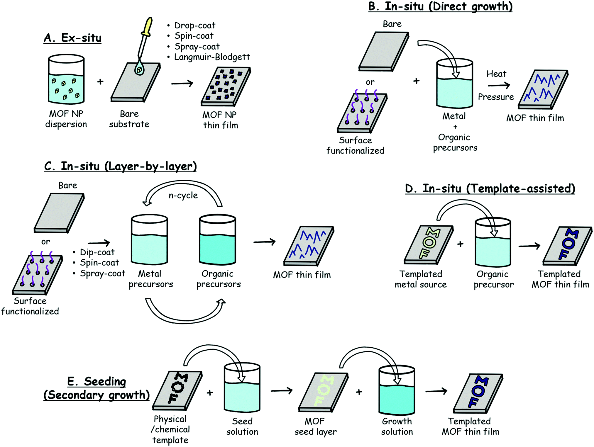 | ||
| Fig. 1 Schematic depictions of the most common MOF thin film synthesis (or deposition) methods. | ||
2. Electrical MOF thin film sensors
Electrical transduction of chemical interactions is a popular sensing approach because of (1) the extensive and well-known capabilities for electrical sensor fabrication and (2) the various electrical-based sensing mechanisms that provide theoretical pathways for enhanced sensitivity and selectivity. The working principle behind electrical chemical sensors is that chemical interactions between the target analyte and sensing material can cause changes in the electronic properties of the sensing material. Mechanisms for this working principle include intramolecular mechanisms (e.g. charge transfer, trap state formation), intermolecular mechanisms (e.g. swelling), or a combination that effects a change in the sensing material's charge concentration, charge mobility, or charge distribution. On the macroscale, these electronic events are reflected as changes in the material's resistance, permittivity (and consequently capacitance), and/or work function. Besides being a selective and sensitive sensing approach, electrical sensors have the additional benefit of potential miniaturization and integration with other electronic devices such as smartphones.MOF thin films have been used as the sensing layer in various types of electrical sensors including chemiresistors, chemicapacitors, and field-effect transistors (FETs).12,47–49 MOF thin film electrical-based sensors are summarized in Table 2. The attraction of using MOFs as the sensing material for electrical sensors lies in their high porosity, chemical tailorability, and potential functionalization. While the majority of MOFs are nonconductive, the advent of conductive MOFs has paved the way for their integration into chemiresistors.50 The dual nature of MOFs creates a variety of potential active sites a target analyte may interact with. For example, reducing gases such as NH3 have strong interactions with open metal sites (OMS),51 while electrophilic analytes like CO2 are more likely to adsorb to a Lewis basic organic ligand.52
| Material | Film growth method | Device type | Target analyte | Sensing range (ppm) | Film thickness (μm) | LOD (ppb) | Ref. |
|---|---|---|---|---|---|---|---|
| Mg-MOF-74 | Solvothermal | Chemicapacitor | Benzene, CO2 | 5–100, 200–5000 | 7.00 | — | 53 |
| Ni-MOF-74 | Metal oxide template | Chemicapacitor | Benzene | 25–100 | 0.09 | — | 54 |
| MFM-300 | Solvothermal | Chemicapacitor | SO2 | 0.075–1 | — | 5 | 55 |
| fum-fcu-MOF | Solvothermal | Chemicapacitor | H2S | 0.1–100 | — | 5 | 56 |
| NbOFFIVE-1-Ni/AlFFIVE-1-Ni | Spin-coat | Chemicapacitor | CO2 | 400–5000 | 2.00 | — | 57 |
| CuBTC | Drop-cast | Chemicapacitor | Methanol, ethanol, isopropanol, acetone | 250–1500 | 8.00 | 61990, 71050, 77800, 100180 |
58 |
| Cu(bdc)·xH2O | LbL | Chemicapacitor | Humidity, VOCs | — | 1.50 | — | 59 |
| CuBTC | Electrochemical | Chemicapacitor | Methanol, ethanol | 200–2000 | 5.00 | 39100, 130000 |
29 |
| NDC-Y-fcu-MOF | Solvothermal | Chemicapacitor | NH3 | 1–100 | — | 92 | 60 |
| Cu3(HITP)2−x(HHTP)x | Spray LbL | Chemiresistor | Benzene | 1–100 | 0.02–0.07 | 24–96 | 61 |
| Cu3(HHTP)(THQ) | Drop-cast | Chemiresistor | NH3 | 1–100 | — | 20–350 | 62 |
| M(Cu, Ni) phthalocyanines, M(Cu, Ni) naphthalocyanines | Drop-cast | Chemiresistor array | NO, H2S, NH3 | 0.02–1, 0.2–80, 2–80 | 1–6 | 1, 19–32, 310–330 | 63 |
| Cu3(HHTP)2/M(Pt, Pd) NPs | Drop-cast | Chemiresistor | NO2 | 1–5 | — | — | 64 |
| Cu3(HHTP)2/Cu3(TCPP)2 | Spray LbL and interface-assisted dip-cast | Chemiresistor | NH3, benzene | 1–100 | 0.075 | 120 (benzene) | 65 |
| Cu3(HIB)2 | Drop-cast | Chemiresistor | CO2 | 400–2500 | — | — | 52 |
| Cu3(HHTP)2 | Spray LbL | Chemiresistor | NH3 | 1–100 | 0.02 | 600 | 66 |
| Ni3(HHTP)2, Ni3(HITP)2 | Solvothermal | Chemiresistor | NO, H2S | 0.1–80, 1–80 | — | 160, 230 | 67 |
| Cu3(HHTP)2, Ni3(HHTP)2 | Solvothermal | Chemiresistor array | NH3, H2S, NO | 2.5–80 | 5–10 | — | 68 |
| Cu3(HHTP)2, Cu3(HITP)2, Ni3(HITP)2 | Drop-cast | Chemiresistor array | VOCs | 200–2500 | — | — | 69 |
| Cu3(HITP)2 | Drop-cast | Chemiresistor | NH3 | 0.5–10 | — | <1000 | 70 |
2.1 Chemiresistive sensors
In its simplest form, a chemiresistor sensing device is composed of two electrodes deposited on an insulating substrate with a conductive sensing material bridging the electrodes. The conductive sensing material serves as a variable resistor in the circuit whereby changes in the chemical environment modulate the resistance of the material. This modulation of resistance can be caused by charge transfer, introduction of electronic trap states or scattering sites that affect charge mobility or shifting of the Schottky barrier between the sensing material and electrode. Due to mismatched energy levels and poor orbital overlap between the metal centers and organic ligands, most 3D MOFs do not display conductivity under ambient conditions. However, the recent advent of conductive 2D MOFs that have in-plane charge delocalization and extended π–d conjugation has led to numerous examples of MOF-based chemiresistors.50 A mechanistic study of these conductive 2D MOFs found that their chemiresistive response towards a target analyte is related to its binding on the OMS of the MOF.51The first example of a MOF-based chemiresistor was prepared from drop-cast films of Cu3(HITP)2 (HITP = 2,3,6,7,10,11-hexaiminotriphenylene), a conductive 2D MOF.70 The electrical conductivity of this MOF can be attributed to the large aromatic core of HITP and favorable orbital overlap between the Cu2+ metal center and the imine base, which results in an extended π–d conjugation network along the ab plane. This 2D MOF displayed a bulk conductivity of 0.2 S cm−1, which is more than enough conductivity to be applied in a chemiresistor device. In this work, bulk Cu3(HITP)2 was synthesized, dispersed in solution, and drop-cast onto interdigitated electrodes (IDEs) to create a chemiresistor device that was sensitive to NH3 vapor. As a continuation of this work, three different conductive 2D MOFs were prepared to construct a cross-reactive sensor array that allowed for clear discrimination of volatile organic compounds (VOCs).69 The three conductive 2D MOFs prepared in this work were Cu3(HITP)2, Ni3(HITP)2, and Cu3(HHTP)2 (HHTP = 2,3,5,6,10,11-hexahydroxytriphenylene). This approach of using chemiresistor arrays in conjunction with principle component analysis (PCA) can provide discrimination between different target analytes and concentration ranges. A recent example of this approach utilized a series of isoreticular nickel metallophthalocyanine (NiPc) and metallonaphthalocyanine (NiNPc) frameworks.63 Frameworks were synthesized by “welding” NiPcs and NiNPcs together with Cu2+ and Ni2+ cations, producing a total of four unique frameworks: NiPc–Ni, Ni–NPc–Ni, NiPc–Cu, and NiNPc–Cu. Compared to single molecule NiPc or NiNPc, welding these subunits into frameworks improved conductivity by 5–7 orders of magnitude. The excellent intrinsic conductivity (up to 10−2 S cm−1) of the frameworks allowed the sensor to be operated at low driving voltages (0.01–1.0 V). PCA applied toward the chemiresistor responses of these conductive MOFs provided discrimination of ppm levels of NO, NH3, and H2S, even in the presence of 18% relative humidity. These NiPc and NiNPc framework chemiresistor sensors displayed excellent sensitivity toward NH3 (limits of detection (LOD): 0.31–0.33 ppm), H2S (LOD: 19–32 ppb), and NO (LOD: 1.0–1.1 ppb).
There have been several examples of in situ growth of conductive 2D MOFs on chemiresistive devices. Mirica and co-workers developed an in situ synthetic method to grow two different conductive 2D MOFs, Cu3(HHTP)2 and Ni3(HHTP)2, on a shrinkable polymer substrate with graphite electrodes.68 Thick films (5–10 μm) of these 2D MOF were grown on a polymer substrate by submerging the substrate in the MOF growth solution for a set time period (Fig. 2A–D). An array of these chemiresistors were able to distinguish between NH3, H2S, and NO (Fig. 2E and F) as well as different concentration ranges (Fig. 2G and H). An advantage of this synthetic method is its adaptability to different substrates. This in situ synthetic method was utilized to grow conductive 2D MOFs on textile fibers, allowing chemiresistor devices to be prepared on fabric.67 The combination of the textile's mesoporosity with the MOF's microporosity makes a device of enhanced porosity that translates into excellent gas sensing ability. At the time of publication, this work showed the best performance of any smart fabric sensor or MOF-based chemiresistor toward NO and H2S detection, displaying LODs for NO and H2S of 0.16 ppm and 0.23 ppm, respectively. Unlike H2S, NO, or NH3, CO2 is not a strong electron donating or accepting molecule, thus it is a difficult target for chemiresistor sensor detection. To address this challenge, chemiresistor devices prepared from Cu3(hexaiminobenzene)2 (Cu3HIB2) thin films were shown to sense practically relevant concentrations of CO2 (400–2500 ppm) with a sensitivity nearly independent of the relative humidity level.52 The high density of NH moieties on hexaiminobenzene promotes the formation of acid–base adducts or bicarbonate salts between CO2 and Cu3HIB2. The formation of these adsorbed CO2 species caused e− withdrawal from the MOF, resulting in charge traps that affected charge mobility and consequently resistance.
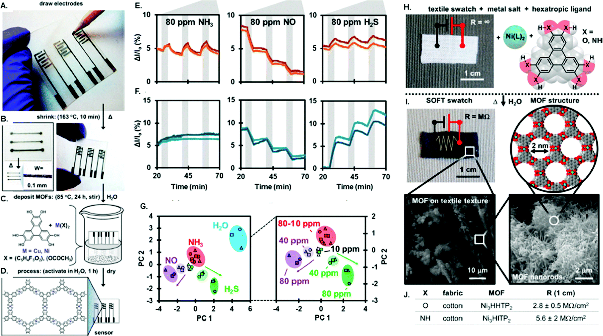 | ||
| Fig. 2 Solution-based growth of 2D conductive MOFs on various substrates. (A) Photograph showing the process of drawing electrodes on a shrinkable polymeric film with a commercial HB (hard black) pencil. (B) Shrinking of the film (10 min, 163 °C) miniaturizes lateral features of the electrodes (W = wire width). (C) Solution-based growth of MOFs onto the device. (D) Schematic illustration of the resulting MOF-based chemiresistive sensors on the surface of a shrinkable polymeric film. Representative sensing traces for (E) Cu3HHTP2 and (F) Ni3HTTP2 exposed to 80 ppm of various gases three times. (G) PCA discrimination of different gases and concentrations. (H) Starting materials for SOFT-sensors: a cotton swatch (no conductivity), the organic triphenylene-based ligand (HHTP or HATP), and metallic node (Ni-(OAc)2 or NiCl2). A photograph of the cotton swatch is shown. (I) Solvothermal condensation of these reagents in water produces conductive smart fabric sensors: textiles coated with nanoporous MOF. Macroscopic through molecular level detail is shown, from a photograph of cotton SOFT sensor postreaction (top left), to scanning electron micrographs detailing MOF coating on fibers (bottom left), and characteristic MOF nanorod texture (bottom right), to space-filling model of MOF (top right). (J) Sheet resistance measurements for smart fabric sensors prepared in this work. (A)–(G) was adapted with permission from J. Am. Chem. Soc., 2016, 28(15), 5264–5268. Copyright 2016 American Chemical Society. (H)–(J) was with permission from J. Am. Chem. Soc. 2017, 139(46), 16759–16767. Copyright 2017 American Chemical Society. | ||
Xu and co-workers were the first to demonstrate thin films (<100 nm) of conductive 2D MOFs integrated into chemiresistor devices (Fig. 3).66 They developed a spray LBL method whereby solutions of the metal precursor and organic ligand of Cu3(HTTP)2, as well as a rinsing solvent, were sequentially sprayed directly onto a chemiresistor device. They found that –OH functionalization on the substrate acted in the same way as a SAM for adhering and orienting MOF thin films. Each spray cycle of this method grew approximately 2 nm of Cu3(HTTP)2 on the device surface. When exposed to NH3 vapor, the Cu3(HTTP)2 chemiresistor displayed an increase in resistance. Ultraviolet photoelectron spectroscopy found that the Fermi level of the Cu3(HTTP)2 film increased by 1.13 eV after exposure to NH3, indicating that NH3 binding was n-type doping in Cu3(HTTP)2, a p-type semiconductor. This spray-coating technique was adapted to grow van der Waals stacked dual MOF thin films directly on chemiresistor devices (Fig. 4).65 In this work, a conductive 2D MOF thin film, Cu-HHTP, was first grown onto the chemiresistor device through spray-coating, followed by the growth of a molecular sieving MOF, Cu-TCPP (tetrakis(4-carboxyphenyl)porphyrin), thin film on top. The sensitivity of only the Cu-HHTP thin film toward NH3 and benzene was tested, and it was found to have a much higher sensitivity to NH3 than benzene because of the electron-donating character of NH3. However, the growth of the molecular sieving Cu-TCPP above Cu-HHTP caused lower sensitivity toward NH3 than benzene, thus reversing the selectivity. This modulation in gas selectivity was caused by the chemisorption of NH3 molecules within the Cu-TCPP layer, which prevents NH3, but not benzene, from reaching the underlying Cu-HHTP thin film.
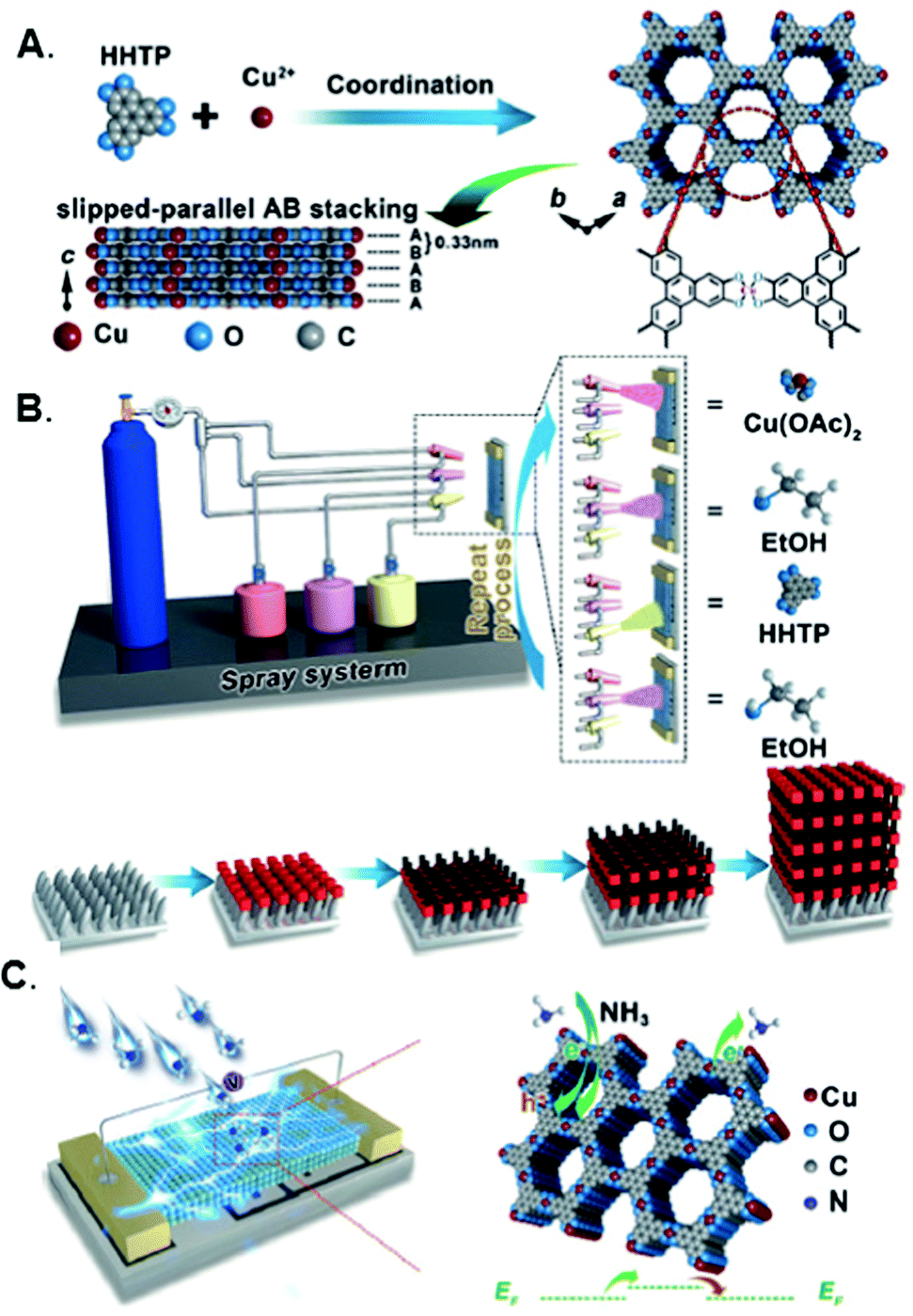 | ||
| Fig. 3 Spray-coating of a 2D conductive MOF thin film on a chemiresistor device. Illustration of (A) the crystal structure of Cu3(HHTP)2 and (B) the preparation of Cu3(HHTP)2 thin-film gas sensors through successive spray-coating of metal linker solution, organic linker solution, and wash solvent. (C) Schematic of the chemiresistor gas sensor and possible gas-sensing mechanism for NH3. This figure was adapted with permission from Angew. Chem., Int. Ed., 2017, 56(52), 16510–16514. Copyright 2017, John C. Wiley and Sons, Inc. | ||
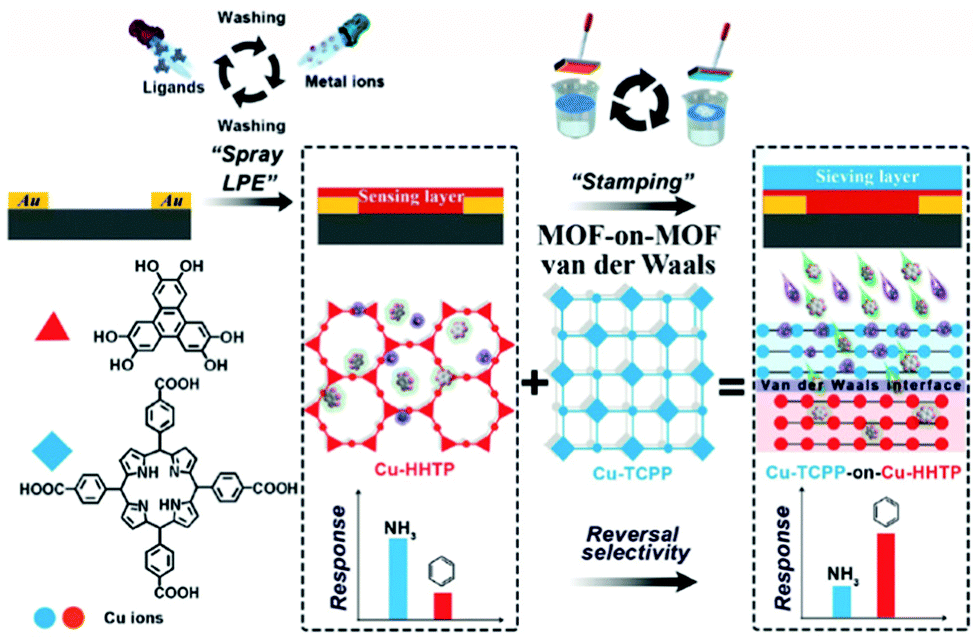 | ||
| Fig. 4 Illustration of the preparation of MOF-on-MOF thin films by van der Waals integration and application of the films as highly selective benzene-sensing materials. This figure was adapted from Angew. Chem., Int. Ed., 2019, 58(42), 14915–14919. Copyright 2019, John C. Wiley and Sons, Inc. | ||
Recent examples of conductive MOFs prepared from a mixture of two ligands have been shown to modulate the sensing properties of these materials as compared to their single-ligand counterparts. Kitagawa, Otake, and co-workers synthesized dual-ligand conductive MOF, Cu3(HHTP)(THQ) (THQ = tetrahydroxy-1,4-quinone), which showed intermediate conductivity and surface area (∼10−5 S cm−1; ∼440 m2 g−1) between Cu3HTTP2 (∼10−3 S cm−1; ∼540 m2 g−1) and Cu3THQ2 (∼10−8 S cm−1; ∼140 m2 g−1).62 A thick film of this dual-ligand MOF was deposited on a chemiresistor device through drop-casting. Surprisingly, the lower conductivity baseline of Cu3(HHTP)(THQ) as compared to Cu3HHTP2 made the dual-ligand MOF more sensitive to small charge transfers, resulting in good discrimination of NH3 at low concentrations (1–100 ppm) and a LOD down to 0.02–0.35 ppm. In another work, Xu and co-workers adapted their spray LBL method to assemble a dual-ligand conductive MOF thin film directly onto a chemiresistive device.61 A mixed ligand solution was used during the spray LBL assembly to produce thin films of Cu3(HHTP)2−x(HITP)x. They observed that HITP doping below 1.0 mol% resulted in a conductivity increase of the MOF thin film; however, doping above 1.0% resulted in decreased conductivity due to diminished crystallinity. Besides conductivity, the selectivity of Cu3(HHTP)2−x(HITP)x toward different gas analytes was modulated by tuning the doping concentration. Selectivity for benzene vs. NH3 was improved 220% for 10 mol% HITP doping as compared to undoped Cu3(HHTP).
2.2 Chemicapacitive sensors
Unlike chemiresistors, which require sensing materials with high conductivities, chemicapacitors can utilize non-conducting materials as the dielectric sensing material. Many examples of non-conductive MOFs integrated as dielectric films in chemicapacitors have been shown well before the first MOF chemiresistor was demonstrated.48 The working principle behind chemicapacitor sensors is the relationship between analyte adsorption in the dielectric material and the subsequent modulation of the material's permittivity constant caused by changes in charge distribution. Both parallel plate design,58 as well as complementary metal oxide semiconductor-compatible IDE design53–57,59,60 have been used to make MOF film-based chemicapacitors. While parallel plate capacitor devices may have higher nominal capacitance and sensitivity, IDE chemicapacitors have the same benefits of IDE chemiresistors, including ease of process, miniaturization, low power consumption, and inexpensive manufacturing cost.71 A challenge of capacitor sensing devices is the requirement for AC, which adds AC frequency as another parameter for optimization. Overall, chemicapacitors are promising devices for the incorporation of MOF thin films because of their simplified IDE design and the requirement for non-conductive sensing materials, of which the majority of MOFs are non-conductive.Achmann and co-workers first demonstrated the integration of non-conductive MOF films on IDE devices by screen-printing MOF pastes on an IDE and heating to evaporate the solvent.72 These devices were coupled to an impedance analyzer to monitor impedance between 1 Hz and 1 MHz in the presence of humidity and VOCs. The first MOF thin film chemicapacitor was demonstrated by Omran and co-workers, wherein crystalline and highly oriented Cu(bdc) thin films were grown on IDE devices functionalized with OH-terminated SAMs through an LBL procedure59 for humidity and VOC sensing. Humidity is a common sensing target for chemicapacitors because of its large molecular dipole (1.85 D) and the high permittivity constant of liquid water (78.3). The choice of MOF used in a sensor must take chemical stability into account for corrosive targets such as H2S and NH3. Salama, Eddouadi, and co-workers developed rare earth (RE) MOFs with face-centered cubic (fcu) topology that are stable even in the presence of corrosive gases. These RE-fcu-MOFs were integrated into IDE capacitor devices via surface functionalization and solvothermal reaction in order to sense H2S or NH3, depending on the organic linker.56,60 RE-fcu-MOF showed stability toward H2S for weeks, in contrast to other more common MOFs like Cu(bdc)·xH2O or ZIF-8, which decomposed due to metal sulfide formation in a short period of time.
Zhao and co-workers demonstrated how the selectivity of MOF chemicapacitors can be modulated with post-synthetic modifications to the MOF sensing layer.53 Mg-MOF-74 films were grown on IDE devices via a solvothermal process and showed sensitivity toward both benzene vapor and CO2. However, after functionalizing the Mg-MOF-74 thin film with ethylenediamine, the chemicapacitor showed an approximately 60% decrease in benzene sensitivity and an approximately 25% increase in CO2 sensitivity. This effect was attributed to ethylenediamine binding to the OMS of Mg-MOF-74, which weakens π-complexation of the benzene molecules to the OMS, and the increased adsorption of CO2 due to amine–CO2 interactions.
Solvothermal syntheses of MOF thin films on surface functionalized devices is the most prevalent synthetic approach for chemicapacitors because of its wide applicability, potential for patterning, and ease-of-use. However, other methods such as electrochemical deposition and the use of metal oxide precursors have also shown success in chemicapacitor preparation.29,54 Yuan et al. compared two synthetic methods for growing Ni-NDC (NDC = 2,6-naphthalenedicarboxylic acid) MOF thin films grown on an IDE device: (1) in situ solvothermal synthesis and (2) Ni(OH)2 precursor conversion (Fig. 5).54 The Ni–NDC MOF thin film grown through the solvothermal method showed poorly adhered, corrugated thin films on the surface of the IDE device. In contrast, MOF growth via a Ni(OH)2 precursor showed compact, homogeneous thin films that displayed no delamination from the substrate. This Ni-NDC thin film IDE device was used to sense benzene down to 25 ppm.
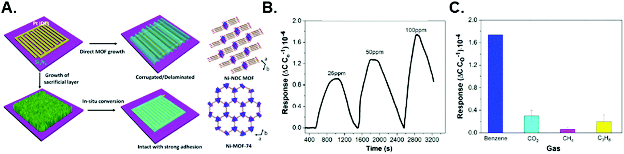 | ||
| Fig. 5 On-chip template-directed conversion of metal hydroxides to MOF thin films as chemicapacitor-based gas sensors. (A) Scheme of direct solvothermal growth on IDE device versus template-directed growth on an IDE device via a sacrificial metal hydroxide layer. (B) Dynamic response of the Ni-NDC MOF-coated capacitive sensor upon exposure to various concentrations of benzene vapor at room temperature. (C) Selectivity of the Ni-NDC MOF-coated sensor toward different analytes. The concentration of benzene is 100 ppm, whereas the concentration of the other gases is 1000 ppm. This figure was adapted with permission from ACS Appl. Mater. Interfaces, 2020, 12(32), 36715–36722. Copyright 2020, American Chemical Society. | ||
2.3 Field effect transistor sensors
Field-effect transistor (FET) sensors are composed of conducting channels (typically the sensing material) that are modulated by electric fields generated by gate electrodes. The gate electrode may be separated from the conductive channel by a solid dielectric layer or a liquid electrolyte solution, depending on the application. The type of gate electrode set-up used in an FET depends on the application. For example, an FET sensor of gases used the solid back-gate architecture, while an FET sensor of aqueous biomolecules would use a liquid gate architecture. There have been few examples of MOF thin films integrated into FET devices.73,74 Duan and co-workers have demonstrated for the first time the application of conductive 2D MOFs, in this case Ni-HTTP, as the conducting channel of an FET sensor.75 In this work, Ni-HTTP thin films were prepared on the surface of an FET device through an interface-assisted/solvothermal synthesis. Briefly, ozone-treated FET devices are contacted with the liquid–air interface of the Ni-HTTP precursor solution and then heated in a water bath at 65 °C for a set time period. The optimal Ni-HTTP FET device showed excellent FET properties with a charge mobility of 45.4 cm2 V−1 s−1 and an on/off current ratio of 2.29 × 10³. A liquid gate composed of phosphate buffer solution and a silver reference electrode was placed above the Ni-HTTP FET device in order to sense different concentrations of gluconic acid in solution. As the gluconic acid concentration increased, the FET's conductance decreased and threshold voltage shifted towards more negative gate voltages, thus demonstrating the potential for a MOF-based FET sensor device.2.4 Device integration considerations for electrical sensors
Defects in MOF film quality such as cracks, inhomogeneity, and poor substrate adhesion can lead to device-to-device variation in electrical properties (e.g. resistance, capacitance), limited device lifetime, and leakage current in the case of alternating current (AC) chemicapacitors.54,58 Moreover, as device miniaturization continues apace, fine area control becomes important for the integration of MOF thin films into devices, especially when incorporating electrically conductive MOF thin films.8 Thus, more sensitive and controllable synthetic methods such as SAM-directed LbL76 and metal oxide templating are crucial for the realization of MOF-based electrical sensors.3. Optical MOF thin film sensors
Optical sensors utilizing MOF thin films offer many advantages, from low equipment costs, rapid response times, and recyclability. Consequentially, it is anticipated that this sensor class will continue to receive significant attention, particularly for the detection of various gases. MOF-based optical sensors rely on changes to the MOF's photofunctional properties (e.g. reflectance,77 refractive index (RI),78 absorbance,79 photoluminescence,13,80–83etc.) in response to interaction with variables of interest, such as ions, gases, and temperature.84,85 Photofunctionality can be introduced into MOF thin films through a variety of ways:86 the use of chromophoric organic linkers within the MOF structures,87 optically-active metal centers (particularly emissive lanthanides),88 or via host–guest interactions, in which photoactive ions,89,90 metal complexes,91,92 molecules,93–96 nanoparticles,97–100 and/or other species are encapsulated by the MOF. MOF-based optical sensors are intriguing because they typically exhibit rapid response times (often on the order of seconds),101–104 high sensitivity (ppb or lower LOD),103,105,106 recyclability (via removal of analyte from the MOF after each sensing cycle),103,104,107–109 and usually can be integrated with inexpensive, portable equipment,90 such as fiber optic-based platforms.104,110,111 Indeed, many optical sensors allow for naked-eye detection of analytes and require only simple laser pointers, light-emitting diodes, UV lamps, or other portable excitation sources for operation.103,112,113 Thus, provided MOF films can be tailored to be sufficiently selective for analytes of interest for “real-world” deployment,114 optical sensors represent a powerful platform for detecting a wide range of analytes. In this section, we describe optical sensing mechanisms, materials, strategies, and techniques using MOF thin films. Table 3 is included here to summarize important parameters from a range of thin-film based-optical sensing studies, with additional details and examples provided in subsequent sections.| Material | Film growth method | Sensing mechanism | Target analyte | Reversible? | Film thickness (μm) | Ref. |
|---|---|---|---|---|---|---|
| [{[Eu(HBPTC)(H2O)2]·2DMF}n] | Electrodeposition | Emission quenching | CO32− | — | 1 | 115 |
| Ln-BTC | Electrodeposition | Emission quenching | Cr3+, nitroaromatics | Yes | 30–70 | 126 |
| {Tb(cpon)(Hcpon)(H2O)3}n | Drop-cast | Emission quenching | Cr2O72− | Yes | — | 127 |
| [Tb2(BDC)3(H2O)4]n | Electrodeposition | Emission quenching | Cu2+ | — | 2 | 128 |
| TbSA | Electrodeposition | Emission quenching | Cu2+ | Yes | 1 | 129 |
| Eu0.24Tb0.76-BHM-COOH | Drop-cast | Emission quenching | Fe3+ | Yes | — | 103 |
| {[Eu2(bqdc)3(H2O)(DMF)3]·0.5DMF·H2O}n | Templated solvothermal | Emission quenching | Hg2+ | — | 10 | 112 |
| Zn2(NDC)2(DPTTZ) | Drop-cast | Emission wavelength shift | Hg2+ | Yes | — | 130 |
| [Tb(L)(H2O)5]n | Thermocompression | Emission quenching | Pb2+ | — | — | 131 |
| [TbL(NO3)3]n·2C4H8O2 | Drop-cast | Ratiometric emission response | Zn2+ | Yes | — | 132 |
| Tb@La-MOF | Spin-coat | Emission quenching | Acetaldehyde | Yes | — | 133 |
| [(CuCN)3L·(guest)x]n | Compression with KBr | Emission wavelength shift | Acetonitrile | Yes | — | 134 |
| Ln(TTA/TAA)@UiO-67 | Templated solvothermal | Emission enhancement | NH3 | — | 50 | 135 |
| {[Tb(TATMA)(H2O)·2H2O}n | Drop-cast | Emission quenching | Antibiotics | — | — | 113 |
| ZIF-8 | Dip-coat | RI change | CO2 | Yes | 0.20 | 104 |
| ZIF-8 | Dip-coat | RI change | CO2 | Yes | 0.25–0.45 | 110 |
| Tb-BTC | Electrodeposition | Emission quenching | 2,4-Dinitrotoluene | — | — | 125 |
| Ru-MOF | Electrodeposition | Emission quenching | Fatty acid binding protein | Yes | 3–17 | 136 |
| Eu-NDC@HPAN | LbL | Emission ratiometric | Formaldehyde | — | 2–4 | 124 |
| UiO-66-(COOH)2–Ag–Eu | Spin-coat | Emission ratiometric | Formaldehyde | — | — | 137 |
| CuBTC | Drop-cast | Absorption decrease | Humidity | Yes | 540 | 138 |
| ZIF-8/PDMS | Dip-coating | RI change | Methane | Yes | 120 | 111 |
| {[Eu2(TDC)3(CH3OH)2]·CH3OH} | Electrodeposition | Emission quenching | Nitroaromatics | Yes | 7 | 139 |
| [NH2(CH3)2]2[Cd17(L)12(μ3-H2O)4(DMF)2(H2O)2]·solvent | Drop-cast | Emission quenching | Nitroaromatics | Yes | — | 140 |
| Zn-BCPA | Drop-cast | Emission quenching | Nitroaromatics | — | 1 | 122 |
| (Zn3(BTC)2) | Electrodeposition | Emission quenching | Nitroaromatics | Yes | 1–18 | 141 |
| CuBTC | Dip-coat | RI change | Nitrobenzene | — | ∼100 | 142 |
| {[Eu2(BCA)3(H2O)(DMF)3]·0.5DMF·H2O}n | Templated solvothermal | Emission quenching | Nitrofuran | Yes | 6 | 107 |
| RPM-3 | Templated solvothermal | Emission enhancement | Olefins | Yes | 3.5 | 121 |
| [Co3(TBTC)2(DMF)2]·4DMF | Templated solvothermal | Absorption wavelength shift | Organic vapors | Yes | 0.58 | 109 |
| CuBTC | Dip-coat | Absorption wavelength shift | Organic vapors | Yes | 0.05–0.1 | 143 |
| NH2-MIL-88B | Spin-coat | Reflection spectroscopy | Organic vapors | Yes | 0.3–1 | 108 |
| Tb(BTC)(H2O) | Dip-coat | Emission quenching | Organic vapors | — | 7 | 144 |
| UiO-66 | Interface-assisted | Reflectance spectroscopy | Organic vapors | Yes | 0.48 | 77 |
| ZIF-8 | Dip-coat | RI change | Organic vapors | Yes | 1 | 78 |
| ZIF-8 | Dip-coat | RI change | Organic vapors | Yes | 0.4 | 145 |
| ZIF-8(Nile red) | Dip-coat | Emission enhancement | Organic vapors | Yes | 0.21 | 96 |
| MIL-100(In):Tb | Solvothermal | Emission quenching | O2 | Yes | 2.5 | 146 |
| Pyrene@ZIF-8 | Dip-coat | Emission quenching | O2 | Yes | — | 147 |
| (H3O)[Zn2L(H2O)]·3NMP·6H2O | Dip-coat | Emission quenching | Pesticides | — | — | 102 |
| MLMOF-3 | Dip-Coat | Emission wavelength shift | Pharmaceuticals | Yes | 4–5 | 123 |
| [Eu4(NDC)6(H2O)5]·3H2O | Electro-deposition | Emission quenching | Picric acid | Yes | 0.05 | 105 |
| Tb@MOF-SO3− | Spin-coat | Emission quenching | trans,trans-Muconic acid | Yes | — | 148 |
| Gd0.9Tb0.1HL | Templated solvothermal | Emission ratiometric | Temperature | Yes | 10 | 149 |
| UiO-66-Eu | Dip-coat | Emission ratiometric | Temperature | — | 30–270 | 150 |
3.1 Luminescence-based sensors
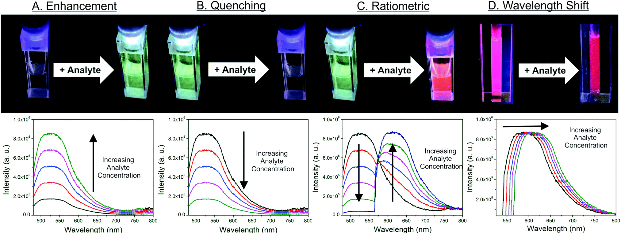 | ||
| Fig. 6 Summary of steady-state luminescence-based sensing mechanisms. (A) Analyte enhances the sensor emission intensity. (B) Analyte reduces, or quenches, the sensor emission intensity. (C) Analyte enhances the intensity of one emission peak and reduces the intensity of a second peak, producing a change in the intensity ratios between the two peaks. (D) The analyte changes the emission energy of the sensor. | ||
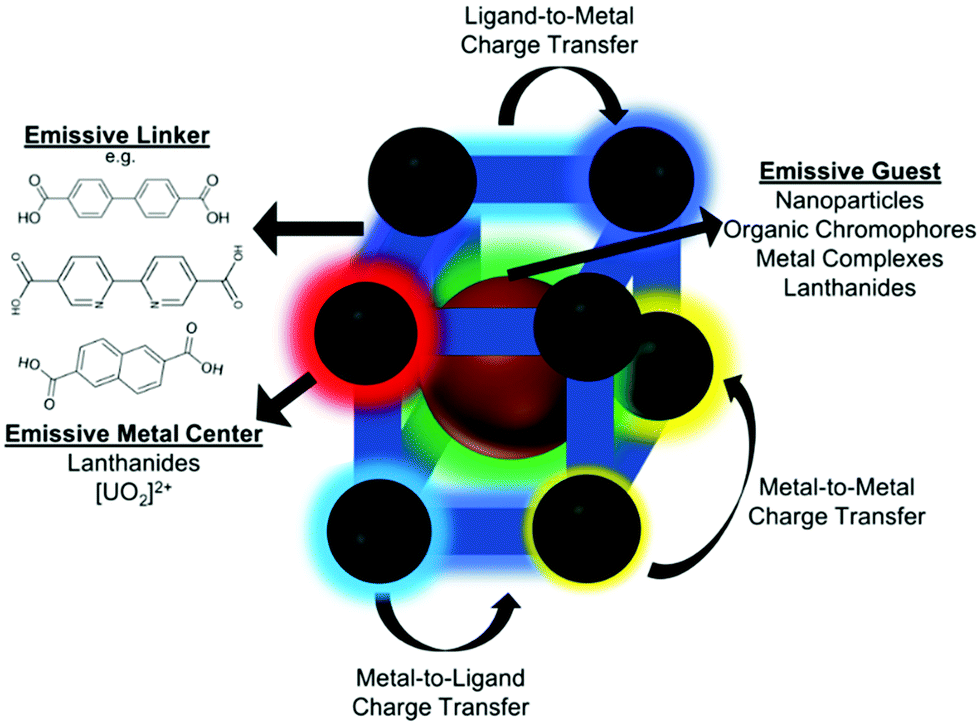 | ||
| Fig. 7 Summary of methods and processes for the design of luminescent MOFs. | ||
In addition to linkers and metal-centers, luminophores may be taken into the MOF pores (e.g. host–guest interactions) to promote luminescence. The luminophore may be added during synthesis for encapsulation136,159,160 or using post-synthetic techniques. Post-synthetic uptake of luminophores may be driven by van der Waals forces,161 electrostatic interactions (i.e. anionic MOFs encapsulating cations),162,163 and/or coordination with unbound functional groups on the linker,164 to name a few examples. Common luminescent guests include lanthanides,101,162 emissive nanoparticles,159 metal complexes,136 and organic molecules.147
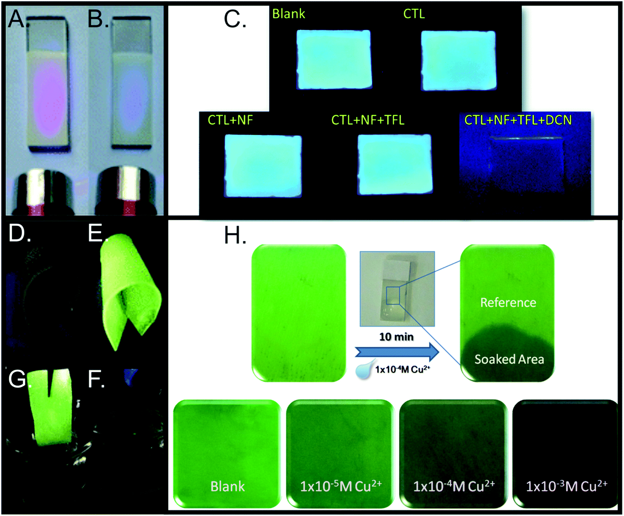 | ||
| Fig. 8 Examples of portable luminescent sensing MOF films. A mercury(II) sensor based on a {[Eu2(bqdc)3(H2O)(DMF)3]·0.5DMF·H2O}n (BQDC = 2,2-biquinoline-4,4-dicarboxylate). Under illumination from a handheld UV light, the MOF film exhibits red Eu-centered emission (A), which is selectivity quenched by mercury ions (B). Reproduced with permission from J. Mater. Chem. A, 2013, 1, 11312–11319. Copyright 2013, Royal Society of Chemistry. (C) A blue-emitting thin film (H3O)[Zn2L(H2O)]·3NMP·6H2O under UV light is exposed to various pesticides (100 μL of 0.01 M solutions): chlorothalonil (CTL), nitrofen (NF), trifluralin (TF), and 2,6-dichloro-4-nitroaniline (DCN). Noticeable quenching is observed in the presence of DCN. Reproduced with permission from RSC Adv., 2019, 9, 38469–38476. Copyright 2019, Royal Society of Chemistry. A flexible film of {[Tb(TATMA)(H2O)·2H2O}n dispersed in a gelatinous glue under ambient (D) and UV (E) light. Emission is quenched upon exposure to 0.5 mM of the antibiotic nitrofurantoin (F), with emission restored upon film removal (G). Reproduced with permission from Inorg. Chem., 2019, 58, 7746–7753. Copyright 2019, American Chemical Society. (H) A film of a terbium-succinate MOF under UV light. The MOF emission is gradually quenched with increasing Cu2+ exposure. Reproduced with permission from Sens. Actuators, B, 2015, 220, 779–787. Copyright 2015, Elsevier, Inc. | ||
| Sensing target | Recycling technique |
|---|---|
| Ions/molecules | Exposure to fresh solvent,103,127,130 chelating agent (e.g. ethylenediaminetetraacetic acid)129 |
| Solvents | Desolvation (heat/vacuum),134,140 drying,133 rinsing with fresh solvent105,107,139 |
| Gases/vapors | Gas purge,104,111,146 vacuum147 |
| Temperature | Temperature change149 |
Ion sensors. The rapid, sensitive, and selective detection of ions has utility in a wide range of areas, including prospecting for high-value elements,90 identifying heavy metal contaminants in water sources,127,131 and medical diagnostics,103,132 for example. MOFs may interact with ions through binding sites within the MOF pores,103,131 or through electrostatic interactions101 (e.g. the use of a cationic MOF to sense anions and anionic MOFs to sense cations). Selective ion detection is often enabled via the inhibition (for “turn off” sensors) or promotion (for “turn on” sensors) of energy transfer states within the MOF upon ion binding.82 For example, Yang and co-workers demonstrated that Cu2+ selectively undergoes partial ion exchange with terbium in a terbium-succinate MOF, which disrupts the sensitization of terbium and reduces emission (Fig. 8H).129 For “turn off” sensors, insights into the emission quenching mechanism may be gained through a Stern–Volmer analysis of the quenching106,168 and through time-resolved studies.169
A key challenge is the development of sensors that exhibit a selective emission response only in the presence of a target ion, hence it is crucial for the sensor to be tested on a multitude of potential interferants that may be encountered in “real-world” systems, such as environmental waters and biological matrices.114 Therefore, cross-sensitivity studies analyzing the impact of competing ions are crucial to evaluating the sensor efficacy. Examples of such studies for ion sensors are shown in Fig. 9.
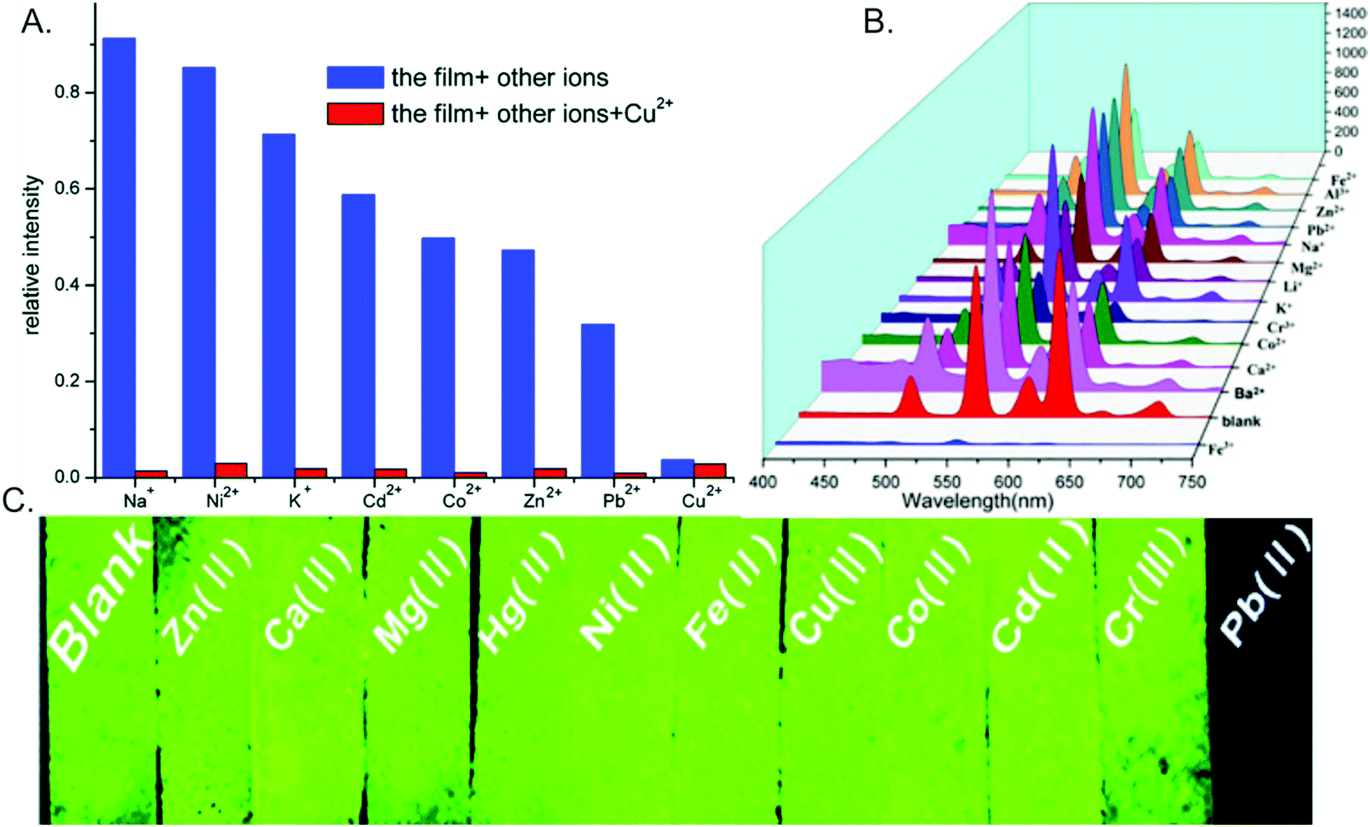 | ||
| Fig. 9 Examples of interferant studies conducted with luminescent MOF thin film ion sensors. (A) Relative emission intensity from [Tb2(BDC)3(H2O)4]n in the presence of 1 mM cation solutions with (red) and without (blue) Cu(II) added. Reproduced with permission from RSC Adv., 2014, 4, 58178–58183. Copyright 2014, Royal Society of Chemistry. (B) Emission spectra of Eu0.24Tb0.76-BHM-COOH in the presence of 0.01 M of various cations. Reproduced with permission from Spectrochim. Acta, Part A, 2020, 230, 118084. Copyright 2020, Elsevier, Inc. (C) Image of [Tb(L)(H2O)5]n under UV light in the presence of 1 mM cation solutions. In each example, quenching is most pronounced selectively for the ion of interest. Reproduced with permission from J. Mater. Chem. A, 2017, 5, 10200–10205. Copyright 2017, Royal Society of Chemistry. | ||
Molecule sensors. In addition to detecting ions in solution, MOF thin films may also be used for the luminescence-based detection of a wide range of molecules, such as solvents,124,133 biomolecules,136,148 and pharmaceuticals.113,123 As such, the thin films have potential utility in medical diagnostics,136 pollution monitoring,105,124,133 and explosives detection,139 among others. The sensing considerations for molecules are similar to those described above for ion detection, in that experimentation in environmentally relevant condition and selectivity studies are both critical. A diversity of sensing mechanisms can be observed for molecular targets. For example, an Eu MOF linked by 2,6-naphthalenedicarboxylate (NDC) grown as a thin film on hydrolyzed polyacetonitrile was selectively degraded by formaldehyde (as evidenced by XRD), leading to a ratiometric response in which emission signal from freed NDC was enhanced while Eu emission was quenched.124 Conversely, a lanthanum MOF with encapsulated Tb ions (Tb@La-MOF) exhibits selective quenching from acetaldehyde exposure without undergoing any structural change. Rather, quenching is observed because an acetaldehyde absorption band overlaps with the Tb@La-MOF excitation band,133 and this competitive absorption mechanism has been exploited for other MOF thin-film sensors as well (Fig. 10).105,139,148
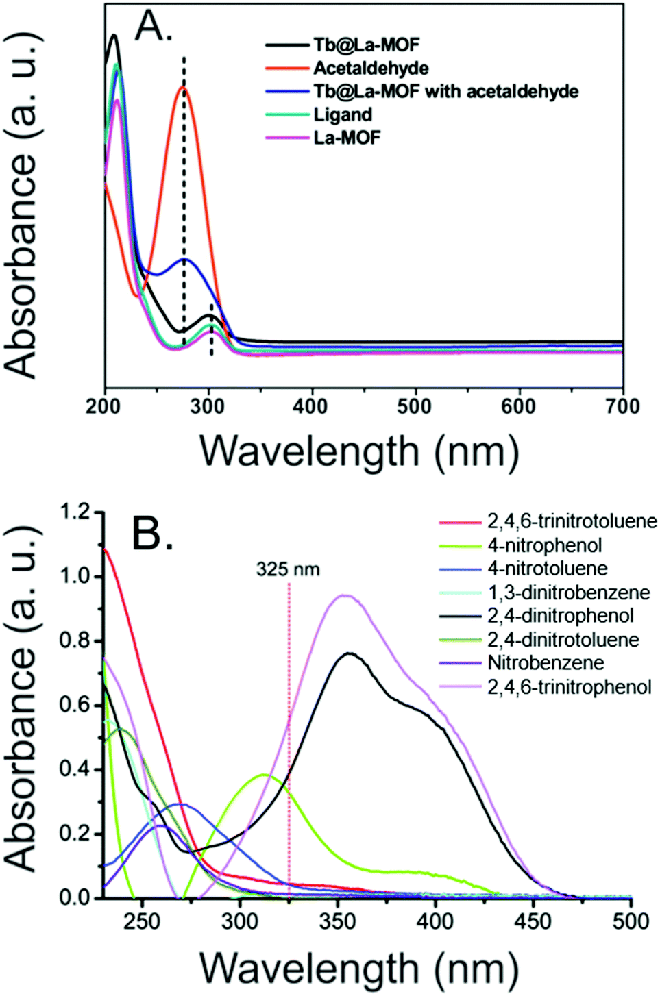 | ||
| Fig. 10 Examples of competitive absorption quenching mechanisms for “turn-off” sensors of molecules. (A) Absorption bands of acetaldehyde overlaps strongly with the excitation band of Tb@La-MOF, causing a selective reduction in emission. Reproduced with permission from Sens. Actuators, B., 2019, 300, 126985. Copyright 2019, Elsevier, Inc. (B) An Eu-TDC MOF selectively detects nitrophenols over other nitroaromatic compounds due to competitive absorption at 325 nm. Reproduced with permission from Analyst, 2016, 141, 4502–4510. Copyright 2016, Royal Society of Chemistry. | ||
In addition to quantitatively detecting individual compounds, MOF thin film sensors have also been designed to distinguish analytes of interest by monitoring responses to multiple emission peaks. For example, a MOF thin film containing both Tb and Eu was developed for distinguishing different pharmaceutical molecules by comparing changes in the intensity ratios of the Tb and Eu peaks following exposure to each molecule (Fig. 11A).123 Similarly, alterations in observed emission color can be used as a visual indicator of the concentration of a single analyte. For example, a thin film of Tb encapsulated by a zinc, 2-sulfonylterephthalate, and 4,4-bipyridine based MOF (MOF-SO3−) on test paper exhibits distinct color changes in the presence of the benzene biomarker trans,trans-muconic acid. This effect is due to quenching of both the Tb and MOF emission peaks, thus providing a pathway towards rapid diagnostics (Fig. 11B).148
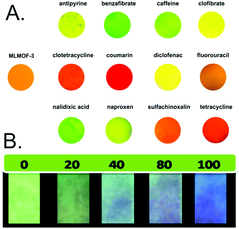 | ||
| Fig. 11 (A) A Tb/Eu mixed lanthanide MOF thin film that provides a visual method for distinguishing various antibiotic molecules. Reproduced with permission from Sens. Actuators, B, 2018, 257, 931–935. Copyright 2018, Elsevier, Inc. (B) A test paper with a thin film of Tb@MOF-SO3− that provides a visual method for rapidly quantifying between 0–100 ppm of trans,trans-muconic acid. Reproduced with permission from Inorg. Chem., 2018, 57, 7815–7824. Copyright 2018, American Chemical Society. | ||
Gas/vapor sensors. MOF thin films may also be employed as luminescent sensors in the gas phase. Often, guest ions/molecules within the MOF pore are used to ensure a selective response upon interaction with target gasses, producing a range of innovative sensing mechanisms. Sensitive sensors for oxygen have been developed based upon the quenching of emission from terbium146 and pyrene147 within MOF hosts. An Eu-functionalized UiO-67 MOF exhibited selective emission enhancement in the presence of ammonia vapors. This enhancement was attributed to hydrogen bonding between the NH3 gas and the MOF linker, which increased the linker triplet state energy and facilitated energy transfer to the Eu (Fig. 12A).135 Similarly, a dual-emissive UiO MOF (zirconium linked with 1,2,4,5-benzenetetracarboxylate) was functionalized with Ag and Eu ions for formaldehyde sensing. When Eu alone is in the MOF, only Eu emission is observed. The presence of Ag+ decreases the energy transfer between the MOF and the Eu, enabling emission peaks from both Eu and the MOF to be observed. Upon formaldehyde interaction with Ag, a ratiometric response occurs in which the Eu peak is enhanced and the MOF peak is quenched (Fig. 12B).137 Nile red dye embedded in a ZIF-8 thin film exhibits a vapor-chromic luminescence response in which non-polar vapors induce a blue-shift in the emission wavelength and more polar vapors induce a red-shift. Importantly, the use of a MOF matrix (relative to Nile Red embedded on a thin film of polystyrene beads) enhanced the sensor sensitivity due to greater interfacial area for vapor interactions (Fig. 12C).96
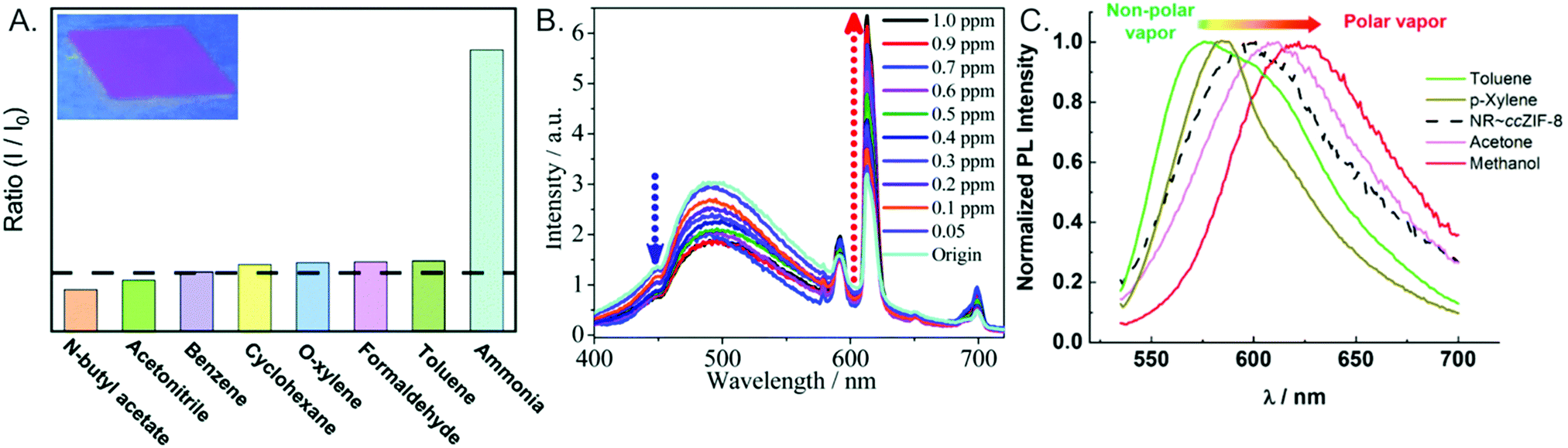 | ||
| Fig. 12 Examples of luminescent MOF thin film vapor sensors. (A) Interaction between ammonia and the linker of an Eu-functionalized UiO-67 MOF leads to enhanced Eu emission (inset: Eu@UiO-67 under 310 nm light). Reproduced with permission from Dalton Trans., 2020, 49, 15663–15671. Copyright 2020, Royal Society of Chemistry. (B) Incorporation of Eu and Ag ions into the pores of a UiO MOF produces a ratiometric response upon formaldehyde interaction with Ag. Reproduced with permission from Nanoscale, 2016, 8, 12047–12053. Copyright 2016, Royal Society of Chemistry. (C) A thin film of Nile Red dye@ZIF-8 exhibits vapor-chromic luminescence upon vapor absorption. Reproduced with permission from Adv. Opt. Mater., 2020, 8, 2000961. Copyright 2020, John C. Wiley & Sons, Inc. | ||
3.2 Absorbance-based sensors
 | ||
| Fig. 13 Examples of typical readouts used in absorbance-based MOF thin film sensors. (A) A Fabry–Pérot device uses ZIF-8 thin films to detect propane vapor (0% to 100%), detected by tracking shifts in the reflectance interference peaks due to RI changes. Reproduced with permission from J. Am. Chem. Soc., 2010, 132, 7832–7833. Copyright 2010, American Chemical Society. (B) ZIF-8 film on an optical fiber detects CO2 gas by monitoring changes in the transmission spectra, which are altered due to a change in RI. Reproduced with permission from ACS Sens., 2018, 3, 386–394. Copyright 2018, American Chemical Society. (C) A thin film of CuBTC on silica beads exhibits gas-dependent shifts in its near-infrared extinction, which is dependent upon the amount of gas absorbed as well as the RI. Reproduced with permission from Adv. Mater., 2011, 23, 4449–4452. Copyright 2011, John C. Wiley & Sons, Inc. | ||
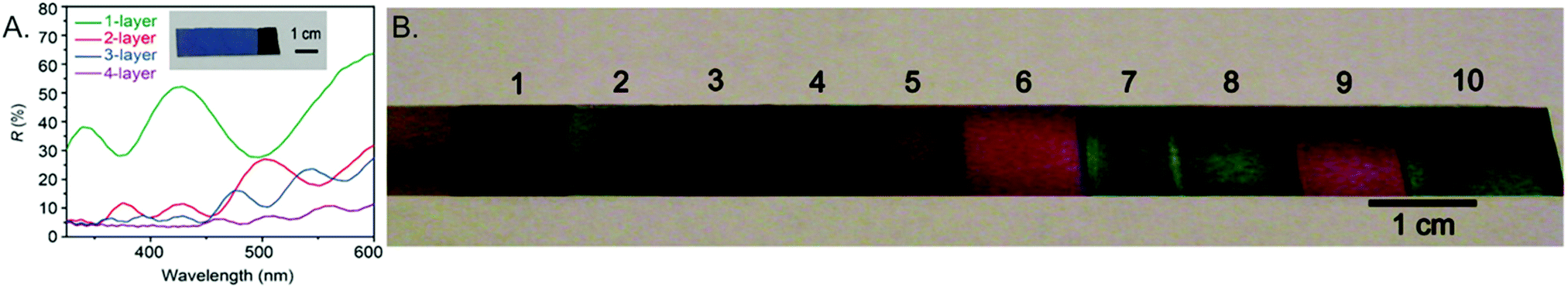 | ||
| Fig. 14 (A) Evolution of the reflectance spectra of UiO-66 monolayers grown on a silicon substrate (inset: photograph of a single monolayer). Both the number and energies of interference peaks change as a function of the MOF layer thickness. Reproduced with permission from ACS Appl. Mater. Interfaces, 2019, 11, 21010–21017. Copyright 2019, American Chemical Society. (B) Photograph of 1 to 10 layers (∼100 to 1000 nm) of ZIF-8 on a silicon substrate. Color changes due to alterations in reflectance are observable to the naked eye. Reproduced with permission from J. Am. Chem. Soc., 2010, 132, 7832–7833. Copyright 2010, American Chemical Society. | ||
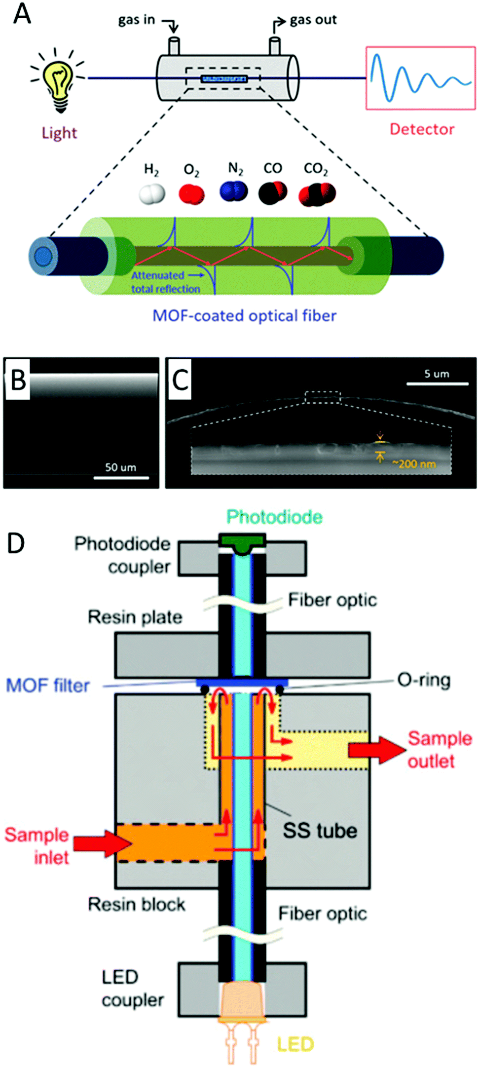 | ||
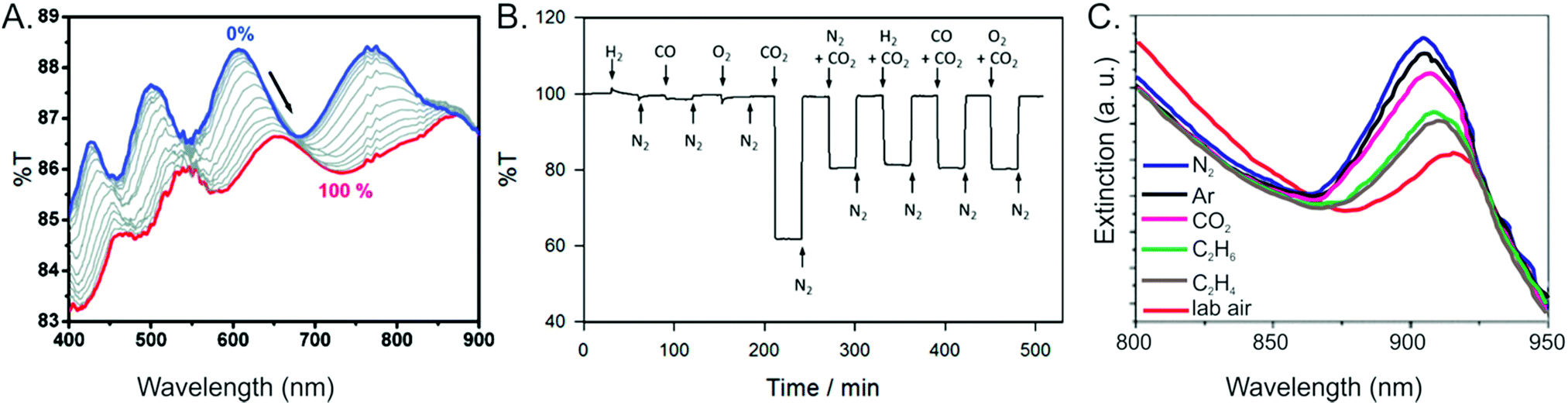
| Fig. 15 Examples of fiber optic MOF thin film sensor platforms. (A) A thin coating of ZIF-8 onto an etched optical fiber is used to detect CO2 selectively over competing gases. (B) Side view and (C) cross-section of the optical fiber functionalized by 200 nm ZIF-8. Reproduced with permission from ACS Sens., 2018, 3, 386–394. Copyright 2018, American Chemical Society. (D) Schematic of a fiber optic humidity sensor using CuBTC as the sensing layer. Reproduced with permission from Anal. Chim. Acta, 2015, 886, 188–193. Copyright 2015, Elsevier, Inc. | ||
Other sensing platforms involve growth of the MOF thin film onto planar substrates, with measurements made either visually or using a spectrometer (e.g.Fig. 14). Rather than being used to detect a single analyte, the sensors typically exhibit different responses to different gases. For example, a composite film of CuBTC and silica beads displays gas-dependent extinction shifts in the NIR, where different pure gases produce different wavelengths of maximum intensity (Fig. 13C).143 Similarly, a film of NH2-MIL-88B (Fe(III) and 2-aminoterephthalic acid) undergoes gas-dependent changes in its reflectance spectrum, enabling visual differentiation of several different pure gases.108 A film of UiO-66 demonstrated a similar response to various organic vapors, including ethanol; a self-assembly growth mechanism producing a mesoporous UiO-66 film significantly outperformed a sensor using a dense UiO-66 layer grown solvothermally, highlighting the important role of the MOF growth technique in sensor development.77
4. Acoustic MOF thin film sensors
Acoustic-based sensors such as QCM and SAW devices have been functionalized with MOF films to great effect. The working principle behind acoustic-based sensors is the relationship between the mass of a piezoelectric crystal and its resonant frequency induced by an alternating electric field. In the case of QCM, small gravimetric changes caused by adsorption on a quartz piezoelectric crystal surface modulate the resonant shear wave frequency across the crystal. This relationship between change in mass (Δm) and frequency (Δf) is described by the Sauerbrey equation (eqn (1)):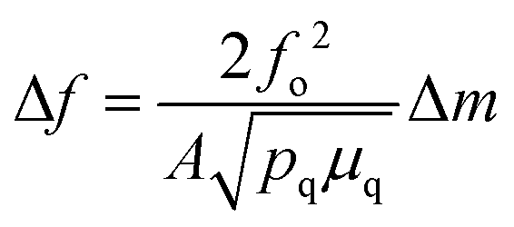 | (1) |
| Material | Film growth method | Device type | Target analyte | Sensing range (ppm or %) | Film thickness (μm) | LOD (ppb) | Ref. |
|---|---|---|---|---|---|---|---|
| CuBTC, MIL-53, CuBPDC | Spray LbL | QCM | VOCs | 1.0–40 | — | — | 175 |
| Chiral and achiral MOF array | LbL | QCM | Chiral/achiral VOCs | 10–100 | — | — | 176 |
| CuBTC | LbL and LPE | Microcantilever | H2O, MeOH, EtOH, CO2 | N/A | 0.1 | — | 187 |
| [Cu2(ndc)2(dabco)]n@[Cu2(NH2-bdc)2(dabco)]n | LbL | QCM | MeOH, hexane | 5–100% | 0.05 | — | 171 |
| CuBTC, MOF-5 | LbL | QCM | VOCs | 100–1000 | 0.5 | 1000 (toluene) | 189 |
| [Zn4O(3,5-dialkylcarboxypyrazolate)3]n-based core–shell | LbL | QCM | VOCs | 1–100% | — | — | 172 |
| MIL-53 | Solvothermal | QCM | Hexane | 3–40% | 3 | — | 190 |
| MIL-101 | Langmuir–Blodgett | QCM | CO2 | 20–100% | 0.05 | — | 20 |
| MIL-96(Al) | Langmuir–Blodgett/Schaefer | QCM | CO2 | 20–100% | 0.2 | — | 186 |
| [Al(OH)(1,4-NDC)] | Drop-cast | QCM | Pyridine vapor | 0.3–25 | — | 40 | 183 |
| KAUST-7, KAUST-8 | Spin-coat | QCM | SO2 | 5–150 | 2 | 5000 | 184 |
| MIL-101 | Drop-cast | QCM | VOCs | 5–700 | 3 | 1603 (pyridine) | 185 |
| MOF-14 | Drop-cast | QCM | Benzene | 0.5–10 | — | 150 | 191 |
| [Cu3(4-(2-carboxyphenoxy)-isophthalic acid)] | QCM | Humidity | 20–96.7% RH | — | — | 192 | |
| CAU-1 | N/A | QCM | Methanol | 32–128 | — | — | 193 |
| MIL-101 | Drop-cast | QCM | Formaldehyde | 2–700 | 3 | 1790 | 194 |
| PIZA-1 | Spray LbL | QCM | Benzene | N/A | 0.340–0.732 | — | 195 |
| ZIF-8 | LPE | QCM/SAW | CO2, CH4 | 1–100%, 20–100% | 0.3 | — | 180 |
| Cu2(ndc)2(dabco) | Metal oxide template | QCM | CO2 | 5–100% | 0.6 | — | 196 |
| MFU-4, MFU-4l | Solvothermal | SAW | CO2 | 1 ppm–100% | 0.2 | 1000 | 179 |
| ZIF-8/ZIF-67 | Spin-coat | SAW | Acetone, ethanol, NH3 | 5–25 | — | 1100, 500, 1600 | 181 |
| CuBTC | LbL | SAW | Humidity | 3–14800 |
0.2 | 280 | 197 |
| UiO-66-NH2 | Spray-coat | Magnetoelastic resonator | Toluene | 3728–8869 | 15 | — | 246 |
4.1 QCM sensors
Dual layer MOF films wherein a “shell” MOF layer chosen for its molecular sieving effect is grown above a “core” MOF layer chosen for its high gas uptake has been successfully demonstrated on QCM-based sensors. A “Janus” film composed of two different MOFs was shown to significantly improve selectivity toward methanol without diminishing sensitivity.171 In this work three films were prepared via LbL growth on a pyridyl-terminated SAM QCM: [Cu2(ndc)2(dabco)]n above [Cu2(HOOC(CH2)2OCNH-bdc)(NH2-bdc)(dabco)]n (A@C), [Cu2(HOOC(CH2)2OCNH-bdc)(NH2-bdc)(dabco)]n grown above [Cu2(ndc)2(dabco)]n (C@A), and a randomly mixed film of [Cu2(ndc)2(dabco)]n and [Cu2(HOOC(CH2)2OCNH-bdc)(NH2-bdc)(dabco)]n (AC). Of the three films, only C@A showed excellent selectivity for methanol and nearly complete exclusion of n-hexane from the QCM surface. This selectivity for methanol over hexane is attributed the small polar pores of [Cu2(HOOC(CH2)2OCNH-bdc)(NH2-bdc)(dabco)]n, which prevent the large non-polar hexane molecules from reaching the underlying [Cu2(ndc)2(dabco)]n layer. The underlying [Cu2(ndc)2(dabco)]n layer has the highest adsorption capacity of the two MOFs, thus sensitivity toward methanol was not diminished. Similar to this work, hierarchical structured core–shell MOF architectures on QCM devices were prepared to achieve highly selective VOC sensors based on size selectivity.172 In this work, small pore “shell” MOF films on large pore “core” MOF films, both based on [Zn4O(3,5-dialkylcarboxypyrazolate)3]n structures, were grown via liquid phase epitaxy (LPE) on QCM devices (Fig. 17). These hierarchical core/shell films were able to selectively adsorb VOC molecules purely based on size while still maintaining high adsorption capacity because of the underlying large pore MOF film. This size exclusion effect was demonstrated with two polar VOCs: methanol and isopropanol. The isotherm of a hierarchical film composed of a small pore shell-layer of [Zn4O(3,5-dialkylcarboxypyrazolate)3]n and a large pore core-layer of [Zn4O(3,5-dimethyl-4-carboxypyrazolate)3]n showed a nearly constant adsorbed amount when the methanol partial pressure was constant and the isopropanol partial pressure was increased. This experiment shows the effectiveness of dual layer MOF films for achieving both molecular sieving and high gas adsorption capacity.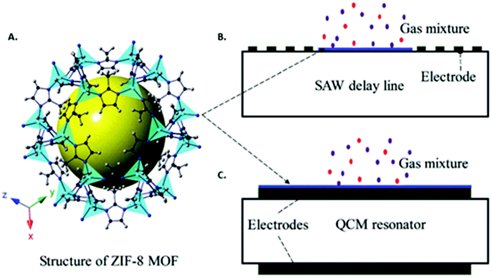 | ||
| Fig. 16 Schematic of (A) a ZIF-8 crystal and its films applied to (B) SAW and (C) QCM transducers. This figure was adapted with permission from Nanoscale, 2018, 10, 8075–8087. Copyright 2018, Royal Society of Chemistry. | ||
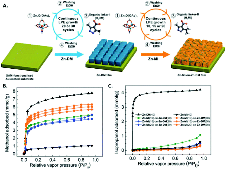 | ||
| Fig. 17 Hierarchical structuring of MOF thin films on QCM substrates for selective adsorption. (A) Schematic illustration of the continuous stepwise LPE fabrication of heterostructured [Zn4O(carboxypyrazolate)3]n thin films, wherein the core-layer MOF is composed of Zn-DM and the shell-layer MOF is composed of Zn-MI. Single-component (b) methanol and (c) isopropanol adsorption isotherms at 25 °C for Zn-MI, Zn-DM and various Zn-MI(x)-on-Zn-DM(y) heterostructured films using an environmental-controlled QCM. Note that x and y represent the number of deposition cycles for Zn-MI and Zn-DM, respectively. This figure was adapted with permission from J. Mater. Chem. A, 2015, 3, 23385–23394. Copyright 2015, Royal Society of Chemistry. | ||
The array approach has been applied to QCM devices in order to discriminate between various gases. The straightforward transduction pathway for QCM, whereby the gas uptake for the partial pressure of a particular gas is directly related to the change in acoustic frequency via the Sauerbrey equation, has allowed for various mathematical investigations into theoretical MOF QCM arrays.173,174 In one of these mathematical studies, a priori data of the gas adsorption properties for individual MOFs, as determined by molecular modelling and simulation, are used to curate the ideal MOF selection for sensor arrays.173 One experimental example of a QCM array composed of three different surface-mounted MOF (SURMOF) thin films (CuBTC, Cu-benzene dicarboxylate, and Cu-biphenyl dicarboxylate) was applied toward the discrimination of different volatile plant oil odors.175 This 3 SURMOF QCM array, in combination with k-nearest neighbour analysis algorithms, was able to discriminate between six VPOs and their binary mixtures with nearly 100% accuracy. Another work constructed a QCM array of 3 chiral MOF and 3 achiral MOFs in order to discriminate between enantiomers of various odor molecules (Fig. 18).176 Interestingly, the chiral MOFs could discriminate between isomer pairs, whereas the achiral MOF devices showed identical responses to isomer pairs. Combination of the chiral and achiral MOF devices into a six-device array led discrimination of five enantiomeric molecule pairs with 96% average accuracy.
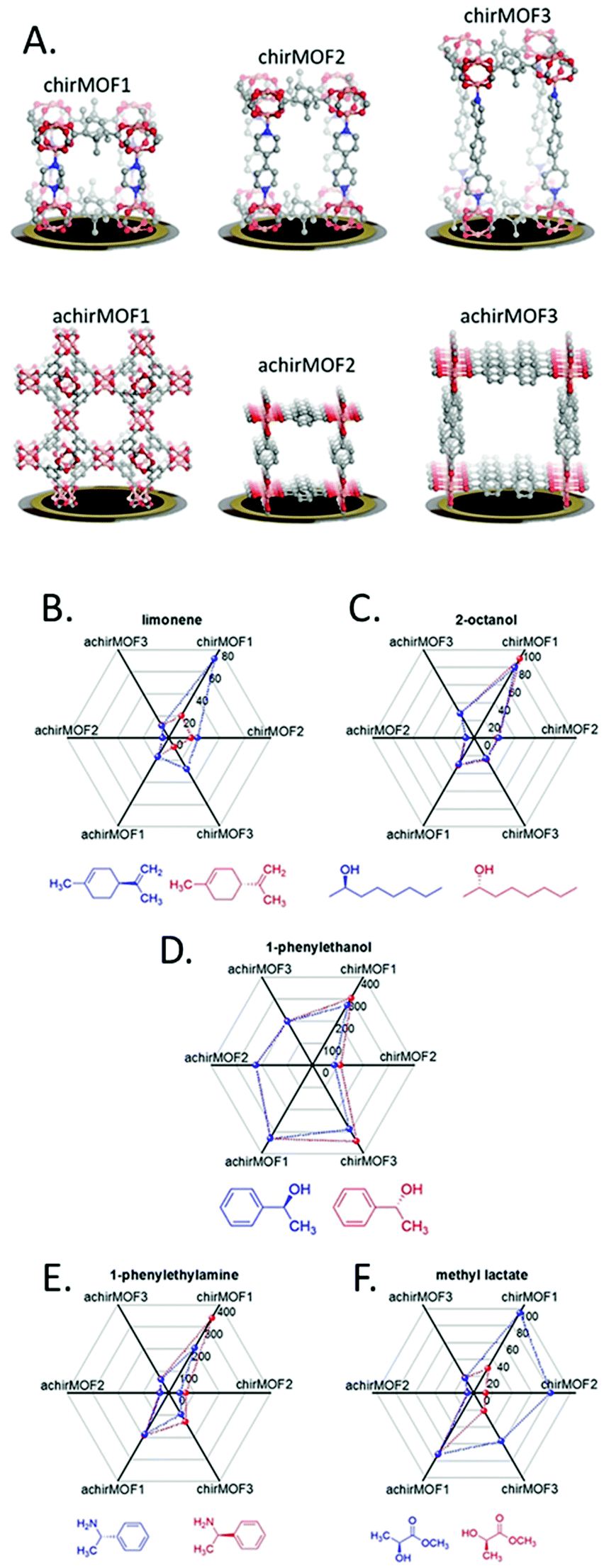 | ||
| Fig. 18 Enantioselective e-nose array prepared with chiral and achiral MOFs. (A) Chiral (top) and achiral (bottom) MOF structures coating the QCM sensors of the e-nose. The term chirMOF1 denotes Cu2(DCam)2-(dabco), chirMOF2 is Cu2(DCam)2(BiPy), chirMOF3 is Cu2(DCam)2-(BiPyB), achirMOF1 is CuBTC, achir-MOF2 is Cu(BDC), and achir-MOF3 is Cu(BPDC). Radar plots of the sensor response to the exposure of (B) (R)- and (S)-limonene, (C) (R)- and (S)-2-octanol, (D) (R)- and (S)-1-phenylethanol, (E) (R)- and (S)-1-phenylethylamine, and (F) methyl (R)- and (S)-lactate. The R-enantiomers are plotted in red, S-enantiomers are plotted in blue. The concentration is 50 ppm. The axes of the radar plots are the negative values of the recorded frequency shifts in Hz at the end of each uptake period, averaged over 40 points. These values correspond to the averaged maximum signals. This figure was adapted with permission from Angew. Chem., Int. Ed., 2021, 60(7), 3566–3571. Copyright 2021, John C. Wiley and Sons, Inc. | ||
4.2 SAW sensors
MOF thin films have been grown on SAW-based sensors as a sensitizing material for various gas sensing applications. In the case of QCM devices, a shear acoustic wave is propagated through the piezoelectric quartz crystal such that only gravimetric changes on the sensing material affect changes in acoustic frequency. In contrast, the acoustic wave in SAW devices runs along the surface of the device and is thus affected by different properties of the sensing material besides gravimetric changes, such as roughness and conductivity. While this adds a complicating factor to SAW in comparison to QCM, SAW devices have the advantage of operating at frequencies 2 to 3 orders of magnitude greater than QCM devices. This higher operating frequency of SAW devices results in increased sensitivity towards gravimetric changes. For example, a ZIF-8 thin film-coated SAW device that operated at a resonant frequency of 860 MHz displayed four times greater sensitivity toward CO2 than a similar ZIF-8 thin film-coated SAW device that operated at a resonant frequency of 430 MHz.177For the reasons mentioned above, thin and uniform sensitizing films are required for SAW-based gas sensors. Therefore, any incorporation of a MOF sensitizing layer must utilize synthetic methods that produce well-controlled thin films on areas typically smaller than 1 cm2. For example, a LbL method was shown to grow dense “nbo” topology MOF thin films (100–200 nm) on the surface of SAW devices with good mechanical coupling.178 These MOF thin film SAW devices were applied toward organic vapor sensing. In another work, a solvothermal method, in conjunction with a small PDMS reaction chamber deposited on the SAW device, was used to grow a thin film of 200 nm MFU-4 NPs.179 The high sensitivity and fast response time of SAW devices made it feasible to perform gas uptake kinetic experiments at different temperatures and to determine the activation energies for a series of different gas uptakes. Liquid-phase epitaxy has been used to directly grow a ZIF-8 thin film on the surface of a Y–Z LiNbO3 SAW device for the detection of CO2 and CH4.180 Interestingly, the same difference in CO2 and CH4 adsorption isotherms for bulk ZIF-8 was reflected in the sensitivity difference of ZIF-8 thin film-coated SAW devices towards these gases. A type of SAW device called Love-wave devices are less affected by roughness or defectiveness of the sensing layer because a low propagation velocity guiding layer (e.g. SiO2) is deposited above the piezoelectric material (e.g. quartz), thus limiting direct interaction between the acoustic wave and the sensing material. Therefore, the use of more rapid but less precise methods such as spin-coating can be used to deposit MOF films. In one example, an array of Love-wave devices spin-coated with ZIF type MOF NPs were used to discriminate between various breath biomarkers such as NH3, acetone, and ethanol.181
4.3 Device integration considerations for acoustic sensors
For QCM, the thickness of the MOF film is proportional to the sensitivity enhancement; however, past a certain thickness the correlation between mass change and frequency change (see Sauerbrey equation) no longer applies. MOF thin films are required for SAW devices since surface acoustic waves decay exponentially perpendicular to the surface.MOF thin films have been grown or deposited on acoustic sensing devices using a variety of methods previously discussed. Similar to electrical sensing devices, methods such as drop-casting and spin-coating have been used to deposit thick films of MOF particles and nanoparticles on acoustic devices.181–185 However, like electrical devices, thick film deposition methods can lead to nanoparticle agglomeration, which causes a loss in surface area and a consequent loss in sensitivity. The large planar dimensions of QCM devices make them well-suited for depositing thin films through the Langmuir–Blodgett (LB) or Langmuir–Schaefer (LS) method, wherein monolayers of MOF NPs at the solution–air interface are deposited on the quartz substrate.20,186 The substrate orientation for LB is perpendicular to the solution surface, whereas the substrate orientation for LS is parallel to the solution surface. The gold electrodes on QCM devices provide a surface for SAM growth, which has been used to grow MOF thin films through LbL methods.171,187–189 Unlike QCM devices, which can function with thick sensing films, the superficial nature of SAWs requires the MOF sensing film on SAW devices to be thin (i.e. hundreds of nanometers).177,179,180Fig. 16 shows schematics of a ZIF-8 film on a QCM and SAW device.
5. Outlook and future directions
5.1 Composite MOF materials
An exciting aspect of MOFs is that they can easily be integrated with a variety of other materials. Indeed, as discussed in Section 3, optical sensors have been developed by exploiting host–guest interactions within the MOF, where lanthanide ions or dyes are used as the sensing material within a MOF scaffold. Beyond dyes or ions, sensors can be designed by combining MOFs with other materials that exhibit unique optical198,199 or physical200 properties,201,202 in which MOF pore functionalities tune selectivity while the second material provides a sensing response. Indeed, a range of MOF thin film composite materials have been developed for sensing applications,203,204 where MOFs have been combined with functional materials such as graphene,205,206 carbon dots,100,207 perovskites,208 polymers,209,210 biomolecules,210 quantum dots,201 and various metal nanoparticles201,210,211 (Fig. 19). In particular, metal NPs encapsulated within conductive MOFs create Schottky junctions at their interface, which act as active sites for analyte adsorption and charge transfer.64 Similarly, metal nanoclusters composed of coinage metals (Cu, Ag, and Au) exhibit surface chemistry-dependent photoluminescence212,213 and can be linked together by rigid organic molecules to form MOFs with unique optical properties.214,215 Emission from powders of these materials has been used for gas sensing applications,216,217 indicating that these MOFs will likely have utility as thin film sensors. In addition to improving sensor performance, integrating MOFs with other materials may improve material stability, an important consideration for sensor deployment.218,219 Another emerging technique is the preparation of thin films comprised of layers of different MOF structures (Fig. 20). The presence of multiple layers of different MOFs can enhance selectivity for analytes of interest by selectively absorbing analytes of interest and blocking potential interferants.220–222 | ||
| Fig. 19 Examples of MOF composite materials. (A) TEM image of an Eu-BTC MOF encapsulates a CH3NH3PBr3 perovskite, producing a dual-emitting film that emits green light under 365 nm excitation (B) and red light under 254 nm excitation (C), reproduced with permission from ACS Appl. Mater. Interfaces, 2018, 10, 27875–27884. Copyright 2018, American Chemical Society. (D) A ZIF-8 film produced with excellent spatial control of gold and platinum nanoparticles is shown in a TEM image, reproduced with permission from Chem. Commun., 2014, 50, 4296–4298. Copyright 2014, Royal Society of Chemistry. (E) An SEM image of polystyrene beads (620 nm) encapsulated by CuBTC MOF, reproduced with permission from Nat. Commun., 2014, 5, 1–9. Copyright 2014, Springer Nature. (F) SEM image of a zinc stilbene MOF encapsulating graphene oxide, reproduced with permission from Nanoscale, 2013, 5, 8533–8540. Copyright 2013, Royal Society of Chemistry. | ||
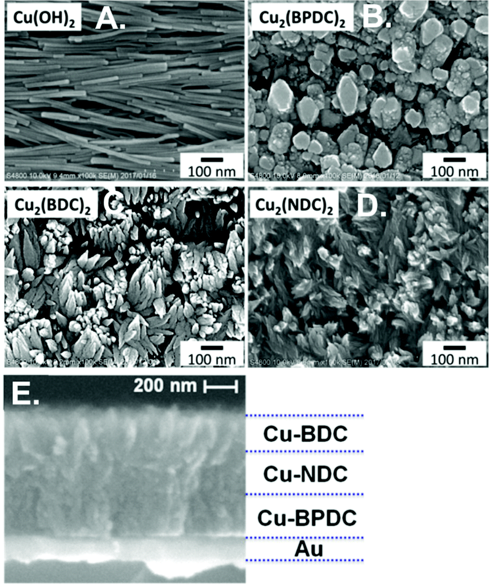 | ||
| Fig. 20 Example of a 4 layer film of (A) Cu(OH)2, (B) Cu2(BPDC)2, (C) Cu2(BDC)2 and (D) Cu2(NDC)2 MOFs, shown in a top-down view by SEM. Reproduced with permission from Angew. Chem., 2019, 131, 6960–6964. Copyright 2019, John C. Wiley and Sons, Inc. (E) SEM of a cross-section of three MOF layers grown on a gold substrate. Reproduced with permission from Nano Lett., 2014, 14, 1526–1529. Copyright 2014, American Chemical Society. | ||
5.2 Synthetic innovations
New synthetic innovations are needed to improve the scalability, quality, and generality (e.g. a method capable of accommodating a range of different MOF structures) of MOF thin film syntheses. One unique emerging method is to synthesize MOFs directly within the system of interest. For example, recently a terbium terephthalate MOF was synthesized within a living plant via immersion of the roots in MOF precursor, enabling luminescent detection of pollutants within the plant over time.223 On-surface vapor-assisted crystallization (or conversion) synthesis224,225 has been introduced as an efficient method in the synthesis of high quality MOF thin films. This method provides a more environmentally friendly process compared to conventional techniques by mitigating chemical waste and eliminating undesired side reactions. Other emerging synthetic processes gaining traction include supersaturation-driven crystallization and continuous flow-fluidic techniques (for liquid phase reactions) and gas phase processes (such as CVD, molecular vapor deposition, and atomic layer deposition), which offer excellent control over MOF film morphology and potential for scalability.226,227 Such innovations are essential for translating MOF thin film technologies from the research lab into industrial-scale, commercial production.2285.3 Emerging sensing techniques
In addition to innovations in materials science, the development of new sensing techniques and platforms will further advance the field. Recently, several MOFs have been designed using qubit arrays and/or the encapsulation of quantum materials,229–233 which may facilitate their use in quantum sensing techniques, an emerging field with the potential to offer unprecedented levels of sensitivity.234,235 Nanocomposite films (Section 5.1) comprised of MOFs and plasmonic structures can be utilized for plasmonic sensing, another important sensing technique in which changes in the plasmon peak intensity or wavelength can track analytes of interest.236 For example, changes in the plasmonic peak of silver nanoparticles (AgNPs) have been used to detect CO2; growing CuBTC over the AgNPs improved the signal 14-fold by concentrating the CO2 near the AgNPs.237 The near-infrared response of indium tin oxide (ITO) nanoparticles to CO2 has similarly been enhanced by CuBTC (Fig. 21A–D).238 A fiber optic sensor comprised of a plasmonic gold film with a MOF coating was shown to sensitively detect alcohol vapors down to a 2.5 ppm level.239 Additionally, plasmonic-MOF nanocomposites have promise in surface enhanced Raman spectroscopy-based sensor applications.240–245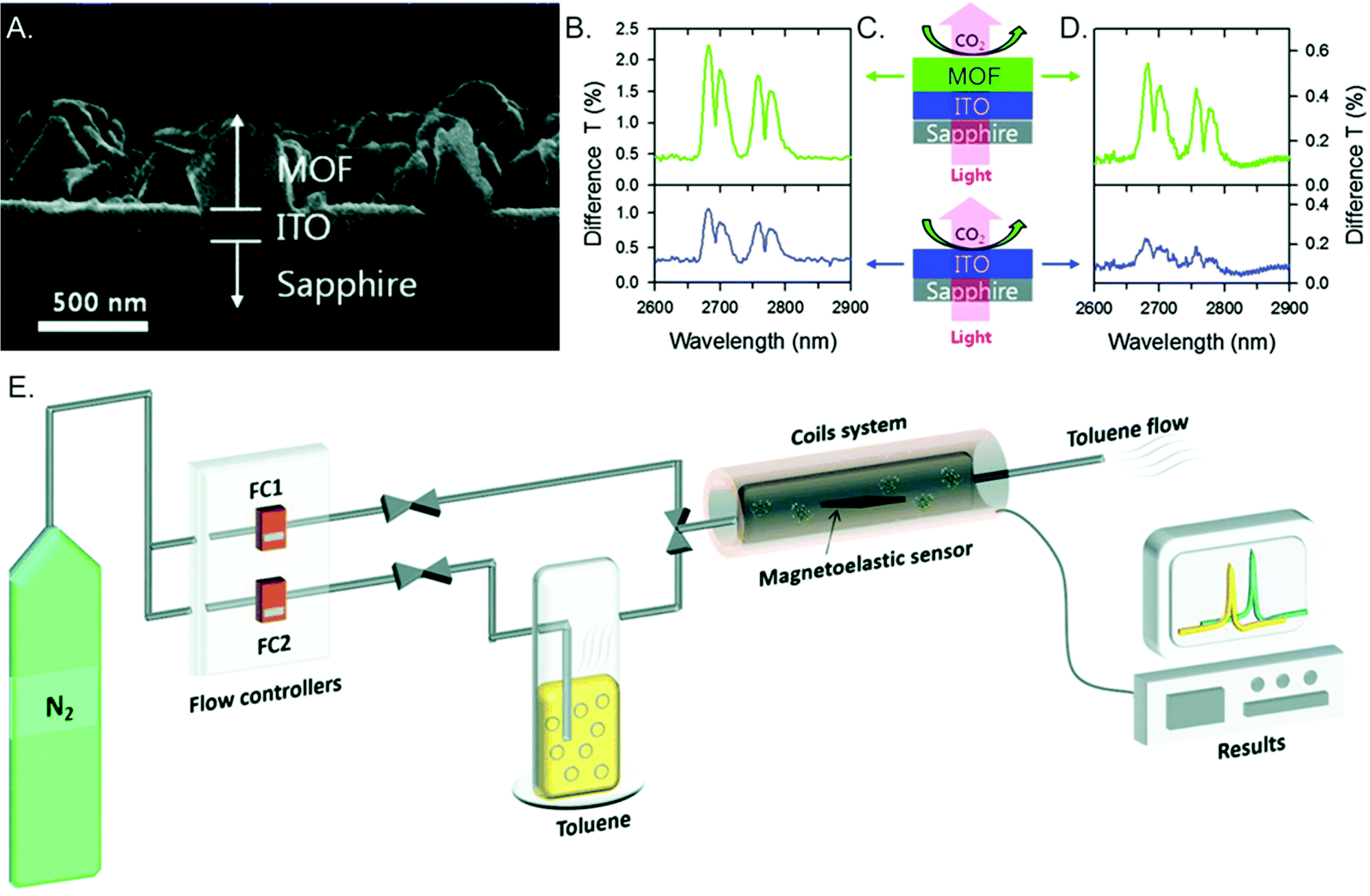 | ||
| Fig. 21 Examples of emerging sensor techniques using MOF thin films. (A) SEM image of a plasmonic sensor consisting of a CuBTC thin film grown on a plasmonic indium tin oxide (ITO) substrate. The sensing response of the ITO plasmon peak from the MOF/ITO composite (top plots) is compared to that of bare ITO (bottom plots) under (B) high (100%) and (D) low (0.1%) CO2 conditions, with schematics of each set-up shown in (C). The presence of the MOF layer significantly enhances the sensor response to CO2. Reproduced with permission from J. Mater. Chem. C, 2015, 3, 2763–2767. Copyright 2015, Royal Society of Chemistry. (E) Schematic of a MOF-coated magnetoelastic sensing apparatus, which was used to detect toluene vapor. Reproduced with permission from J. Mater. Chem. C, 2020, 8, 13743–13753. Copyright 2020, Royal Society of Chemistry. | ||
A magnetoelastic sensor technique was recently demonstrated, in which UiO-66-NH2 was spray-coated onto a rhombic-shaped strip of a ferromagnetic alloy, which could be used as a wireless sensor for toluene. Similar to SAW devices, a magnetoelastic sensor operates based upon the impact of mass change on the magnetoelastic resonance frequency.246 The relatively simple fabrication process and high sensitivity indicate that MOF-based magnetoelastic sensors are worthy of additional study and optimization (Fig. 21E).
5.4 Challenges
The ubiquity of water presents a challenge for most sensor applications, especially when utilizing a new material class like MOFs. The sensing of ions or other chemical species in water, as well as any sensing application done in humid environments, necessitates the use of materials that are (1) stable in aqueous solution or water vapor and (2) selective to the target analyte even in the presence of water. While water stability for the most studied MOF materials (e.g. CuBTC, ZIF-8) have been thoroughly investigated, the water stability of the majority of synthesized MOF materials have yet to be investigated. Though a thorough investigation must be done if a particular MOF thin film will be utilized as a sensing material, a few rules of thumb can be used to predict the relative stability and selectivity against water: (1) the absence of OMS, (2) hydrophobic organic ligands, and (3) strong metal–organic bonds (e.g. M(III)–carboxylate bonds). Post-functionalization of MOF thin films and compositing MOFs with hydrophobic polymer are two methods that have been applied to mitigate the negative effects of water.247–249Beyond proof-of-principle and developmental testing in laboratory settings, consideration for the processability of MOF thin films within a sensor device architecture is required for any large-scale fabrication. Processability of a material includes factors such as device-to-device variability, patterning resolution, and processing time. Research into the integration of MOF thin films in electronic microdevices has found that a combination of bottom-up syntheses such as metal oxide templating with top-down methods such as photo- or e-beam lithography can be utilized to pattern MOF thin films within devices.8,44,250–253 A recent example applied X-ray lithography and e-beam lithography to halogenated ZIF thin films (grown via chemical vapour deposition) to achieve film patterning with resolution reaching 10 μm and 50 nm, respectively.254
6. Conclusions
Synthetic innovations enabling the development of MOF thin films have produced a range of exciting sensing technologies, capable of sensitive and selective detection of a range of analytes, including ions, small molecules, gases, temperature, and other analytes of interest using optical, electrical, and acoustic techniques. MOF thin film technologies have the potential to significantly benefit energy, manufacturing, environmental, and medical sectors, among others. Fulfilling this potential requires (1) continued synthetic innovations to stabilize MOF thin films in harsh environments (e.g. high temperature, humidity, corrosive atmosphere, etc.), (2) developing strategies for mass production of thin films, and (3) continued innovations in the development of sensing techniques and platforms. Addressing such barriers to commercialization will be crucial for translating this transformative class of MOF sensing materials from the research lab into everyday products.Notes
Neither the United States Government nor any agency thereof, nor any of its employees, nor the support contractor, nor any of their employees, makes any warranty, express or implied, or assumes any legal liability or responsibility for the accuracy, completeness, or usefulness of any information, apparatus, product, or process disclosed, or represents that its use would not infringe privately owned rights. Reference herein to any specific commercial product, process, or service by trade name, trademark, manufacturer, or otherwise does not necessarily constitute or imply its endorsement, recommendation, or favoring by the United States Government or any agency thereof. The views and opinions of authors expressed herein do not necessarily state or reflect those of the United States Government or any agency thereof.Author contributions
The manuscript was written through contributions of all authors. All authors have given approval to the final version of the manuscript.Conflicts of interest
There are no conflicts to declare.Acknowledgements
James E. Ellis and Scott E. Crawford are grateful for funding through the National Energy Technology Research Participation Program, sponsored by the U.S. Department of Energy and administered by the Oak Ridge Institute for Science Education. We thank Eunchae Kim for her assistance with the scheme. This project was funded by the Department of Energy, National Energy Technology Laboratory an agency of the United States Government, through a support contract.References
- P. Z. Moghadam, A. Li, S. B. Wiggin, A. Tao, A. G. P. Maloney, P. A. Wood, S. C. Ward and D. Fairen-Jimenez, Chem. Mater., 2017, 29, 2618 CrossRef CAS.
- B. F. Hoskins and R. Robson, J. Am. Chem. Soc., 1990, 112, 1546 CrossRef CAS.
- S. S.-Y. Chui, S. M.-F. Lo, J. P. Charmant, A. G. Orpen and I. D. Williams, Science, 1999, 283, 1148 CrossRef CAS PubMed.
- H. Li, M. Eddaoudi, M. O'Keeffe and O. M. Yaghi, Nature, 1999, 402, 276 CrossRef CAS.
- T. Liu, P. Li, N. Yao, T. Kong, G. Cheng, S. Chen and W. Luo, Adv. Mater., 2019, 31, 1806672 CrossRef PubMed.
- K. J. Erickson, F. Léonard, V. Stavila, M. E. Foster, C. D. Spataru, R. E. Jones, B. M. Foley, P. E. Hopkins, M. D. Allendorf and A. A. Talin, Adv. Mater., 2015, 27, 3453 CrossRef CAS PubMed.
- V. Stavila, A. A. Talin and M. D. Allendorf, Chem. Soc. Rev., 2014, 43, 5994 RSC.
- I. Stassen, N. Burtch, A. Talin, P. Falcaro, M. Allendorf and R. Ameloot, Chem. Soc. Rev., 2017, 46, 3185 RSC.
- J. Liu and C. Wöll, Chem. Soc. Rev., 2017, 46, 5730 RSC.
- O. Shekhah, J. Liu, R. Fischer and C. Wöll, Chem. Soc. Rev., 2011, 40, 1081 RSC.
- X. Ma, Y. Chai, P. Li and B. Wang, Acc. Chem. Res., 2019, 52, 1461 CrossRef CAS PubMed.
- A. Chidambaram and K. C. Stylianou, Inorg. Chem. Front., 2018, 5, 979 RSC.
- Y. Zhang, S. Yuan, G. Day, X. Wang, X. Yang and H.-C. Zhou, Coord. Chem. Rev., 2018, 354, 28 CrossRef CAS.
- W.-J. Li, M. Tu, R. Cao and R. A. Fischer, J. Mater. Chem. A, 2016, 4, 12356 RSC.
- Y. Zhang and C.-H. Chang, Processes, 2020, 8, 377 CrossRef CAS.
- Z.-G. Gu and J. Zhang, Coord. Chem. Rev., 2019, 378, 513 CrossRef CAS.
- L. J. Small and T. M. Nenoff, ACS Appl. Mater. Interfaces, 2017, 9, 44649 CrossRef CAS PubMed.
- D. Jiang, A. D. Burrows, Y. Xiong and K. J. Edler, J. Mater. Chem. A, 2013, 1 Search PubMed.
- L. D. Sappia, J. S. Tuninetti, M. Ceolin, W. Knoll, M. Rafti and O. Azzaroni, Glob. Chall., 2020, 4, 1900076 CrossRef PubMed.
- J. Benito, S. Sorribas, I. Lucas, J. Coronas and I. Gascon, ACS Appl. Mater. Interfaces, 2016, 8, 16486 CrossRef CAS PubMed.
- P. Goel, S. Singh, H. Kaur, S. Mishra and A. Deep, Sens. Actuators, B, 2021, 329, 129157 CrossRef CAS.
- L. Fontana, I. Fratoddi, I. Venditti, D. Ksenzov, M. V. Russo and S. Grigorian, Appl. Surf. Sci., 2016, 369, 115 CrossRef CAS.
- K. Zhao, X. Yu, R. Li, A. Amassian and Y. Han, J. Mater. Chem. C, 2015, 3, 9842 RSC.
- B. K. Kuila and M. Stamm, Macromol. Sym., 2011, 303, 85 CrossRef CAS.
- D. Zacher, O. Shekhah, C. Woll and R. A. Fischer, Chem. Soc. Rev., 2009, 38, 1418 RSC.
- C. S. Kim, S. Lee, E. D. Gomez, J. E. Anthony and Y.-L. Loo, Appl. Phys. Lett., 2008, 93, 103302 CrossRef.
- N. Patra, M. Salerno, A. Diaspro and A. Athanassiou, J. Mater. Sci., 2011, 46, 5044 CrossRef CAS.
- G. Bussetti, S. Trabattoni, S. Uttiya, A. Sassella, M. Riva, A. Picone, A. Brambilla, L. Duò, F. Ciccacci and M. Finazzi, Synth. Met., 2014, 195, 201 CrossRef CAS.
- M. S. Hosseini, S. Zeinali and M. H. Sheikhi, Sens. Actuators, B, 2016, 230, 9 CrossRef CAS.
- E. A. Gaulding, B. T. Diroll, E. D. Goodwin, Z. J. Vrtis, C. R. Kagan and C. B. Murray, Adv. Mater., 2015, 27, 2846 CrossRef CAS PubMed.
- Z. Fu and G. Xu, Chem. Rec., 2017, 17, 518 CrossRef CAS PubMed.
- H. Ohara, S. Yamamoto, D. Kuzuhara, T. Koganezawa, H. Oikawa and M. Mitsuishi, ACS Appl. Mater. Interfaces, 2020, 12, 50784 CrossRef CAS PubMed.
- N. Nijem, K. Fürsich, S. T. Kelly, C. Swain, S. R. Leone and M. K. Gilles, Cryst. Growth Des., 2015, 15, 2948 CrossRef CAS.
- V. Chernikova, O. Shekhah and M. Eddaoudi, ACS Appl. Mater. Interfaces, 2016, 8, 20459 CrossRef CAS PubMed.
- Z. Wang and C. Wöll, Adv. Mater. Technol., 2018, 4, 1800413 CrossRef.
- X. Zhang, K. Wan, P. Subramanian, M. Xu, J. Luo and J. Fransaer, J. Mater. Chem. A, 2020, 8, 7569 RSC.
- Y. Yoo and H. K. Jeong, Chem. Commun., 2008, 2441 RSC.
- Y. Yue, Z.-A. Qiao, X. Li, A. J. Binder, E. Formo, Z. Pan, C. Tian, Z. Bi and S. Dai, Cryst. Growth Des., 2013, 13, 1002 CrossRef CAS.
- Z.-Q. Li, M. Zhang, B. Liu, C.-Y. Guo and M. Zhou, Inorg. Chem. Commun., 2013, 36, 241 CrossRef CAS.
- Y. Yue, N. Mehio, A. J. Binder and S. Dai, CrystEngComm, 2015, 17, 1728 RSC.
- S. E. Crawford, K.-J. Kim, Y. Yu and P. R. Ohodnicki, Cryst. Growth Des., 2018, 18, 2924 CrossRef CAS.
- P.-C. Guo, T.-Y. Chen, X.-M. Ren, Z. Chu and W. Jin, J. Mater. Chem. A, 2014, 2, 13698 RSC.
- A. Demessence, C. Boissière, D. Grosso, P. Horcajada, C. Serre, G. Férey, G. J. Soler-Illia and C. Sanchez, J. Mater. Chem., 2010, 20, 7676 RSC.
- I. Stassen, M. Styles, G. Grenci, H. Van Gorp, W. Vanderlinden, S. De Feyter, P. Falcaro, D. De Vos, P. Vereecken and R. Ameloot, Nat. Mater., 2016, 15, 304 CrossRef CAS PubMed.
- T. Stassin, S. Rodríguez-Hermida, B. Schrode, A. J. Cruz, F. Carraro, D. Kravchenko, V. Creemers, I. Stassen, T. Hauffman and D. De Vos, Chem. Commun., 2019, 55, 10056 RSC.
- I. Stassen, D. De Vos and R. Ameloot, Chem. – Eur. J., 2016, 22, 14452 CrossRef CAS PubMed.
- M. G. Campbell and M. Dinca, Sensors, 2017, 17, 1108 CrossRef PubMed.
- H. Y. Li, S. N. Zhao, S. Q. Zang and J. Li, Chem. Soc. Rev., 2020, 49, 6364 RSC.
- M.-S. Yao, W.-H. Li and G. Xu, Coord. Chem. Rev., 2021, 426, 213479 CrossRef CAS.
- L. S. Xie, G. Skorupskii and M. Dinca, Chem. Rev., 2020, 120, 8536 CrossRef CAS PubMed.
- V. Rubio-Gimenez, N. Almora-Barrios, G. Escorcia-Ariza, M. Galbiati, M. Sessolo, S. Tatay and C. Marti-Gastaldo, Angew. Chem., Int. Ed., 2018, 57, 15086 CrossRef CAS PubMed.
- I. Stassen, J. H. Dou, C. Hendon and M. Dinca, ACS Cent. Sci., 2019, 5, 1425 CrossRef CAS PubMed.
- H. Yuan, J. Tao, N. Li, A. Karmakar, C. Tang, H. Cai, S. J. Pennycook, N. Singh and D. Zhao, Angew. Chem., Int. Ed., 2019, 58, 14089 CrossRef CAS PubMed.
- H. Yuan, J. Cui, N. Li, M. Li, X. Yu, W. Fan, A. Karmakar, J. Dong, S. J. Pennycook, H. Cai and D. Zhao, ACS Appl. Mater. Interfaces, 2020, 12, 36715 CrossRef CAS PubMed.
- V. Chernikova, O. Yassine, O. Shekhah, M. Eddaoudi and K. N. Salama, J. Mater. Chem. A, 2018, 6, 5550 RSC.
- O. Yassine, O. Shekhah, A. H. Assen, Y. Belmabkhout, K. N. Salama and M. Eddaoudi, Angew. Chem., Int. Ed., 2016, 55, 15879 CrossRef CAS PubMed.
- M. R. Tchalala, Y. Belmabkhout, K. Adil, K. N. Chappanda, A. Cadiau, P. M. Bhatt, K. N. Salama and M. Eddaoudi, ACS Appl. Mater. Interfaces, 2018, 11, 1706 CrossRef PubMed.
- S. Homayoonnia and S. Zeinali, Sens. Actuators, B, 2016, 237, 776 CrossRef CAS.
- C. Sapsanis, H. Omran, V. Chernikova, O. Shekhah, Y. Belmabkhout, U. Buttner, M. Eddaoudi and K. N. Salama, Sensors, 2015, 15, 18153 CrossRef CAS PubMed.
- A. H. Assen, O. Yassine, O. Shekhah, M. Eddaoudi and K. N. Salama, ACS Sens., 2017, 2, 1294 CrossRef CAS PubMed.
- A.-Q. Wu, W.-Q. Wang, H.-B. Zhan, L.-A. Cao, X.-L. Ye, J.-J. Zheng, P. N. Kumar, K. Chiranjeevulu, W.-H. Deng, G.-E. Wang, M.-S. Yao and G. Xu, Nano Res., 2020, 14, 438 CrossRef.
- M. S. Yao, J. J. Zheng, A. Q. Wu, G. Xu, S. S. Nagarkar, G. Zhang, M. Tsujimoto, S. Sakaki, S. Horike, K. Otake and S. Kitagawa, Angew. Chem., Int. Ed., 2020, 59, 172 CrossRef CAS PubMed.
- Z. Meng, A. Aykanat and K. A. Mirica, J. Am. Chem. Soc., 2019, 141, 2046 CrossRef CAS PubMed.
- W. T. Koo, S. J. Kim, J. S. Jang, D. H. Kim and I. D. Kim, Adv. Sci., 2019, 6, 1900250 CrossRef CAS PubMed.
- M. S. Yao, J. W. Xiu, Q. Q. Huang, W. H. Li, W. W. Wu, A. Q. Wu, L. A. Cao, W. H. Deng, G. E. Wang and G. Xu, Angew. Chem., Int. Ed., 2019, 58, 14915 CrossRef CAS PubMed.
- M. S. Yao, X. J. Lv, Z. H. Fu, W. H. Li, W. H. Deng, G. D. Wu and G. Xu, Angew. Chem., Int. Ed., 2017, 56, 16510 CrossRef CAS PubMed.
- M. K. Smith and K. A. Mirica, J. Am. Chem. Soc., 2017, 139, 16759 CrossRef CAS PubMed.
- M. K. Smith, K. E. Jensen, P. A. Pivak and K. A. Mirica, Chem. Mater., 2016, 28, 5264 CrossRef CAS.
- M. G. Campbell, S. F. Liu, T. M. Swager and M. Dinca, J. Am. Chem. Soc., 2015, 137, 13780 CrossRef CAS PubMed.
- M. G. Campbell, D. Sheberla, S. F. Liu, T. M. Swager and M. Dinca, Angew. Chem., Int. Ed., 2015, 54, 4349 CrossRef CAS PubMed.
- S. Zeinali, S. Homayoonnia and G. Homayoonnia, Sens. Actuators, B, 2019, 278, 153 CrossRef CAS.
- S. Achmann, G. Hagen, J. Kita, I. M. Malkowsky, C. Kiener and R. Moos, Sensors, 2009, 9, 1574 CrossRef CAS PubMed.
- X. Huang, P. Sheng, Z. Tu, F. Zhang, J. Wang, H. Geng, Y. Zou, C. A. Di, Y. Yi, Y. Sun, W. Xu and D. Zhu, Nat. Commun., 2015, 6, 7408 CrossRef CAS PubMed.
- G. Wu, J. Huang, Y. Zang, J. He and G. Xu, J. Am. Chem. Soc., 2017, 139, 1360 CrossRef CAS PubMed.
- B. Wang, Y. Luo, B. Liu and G. Duan, ACS Appl. Mater. Interfaces, 2019, 11, 35935 CrossRef CAS PubMed.
- H. J. Park, M. C. So, D. Gosztola, G. P. Wiederrecht, J. D. Emery, A. B. Martinson, S. L. Er, C. E. Wilmer, N. A. Vermeulen and A. Aspuru-Guzik, ACS Appl. Mater. Interfaces, 2016, 8, 24983 CrossRef CAS PubMed.
- R. Zhang, D. Zhang, Y. Yao, Q. Zhang, Y. Xu, Y. Wu, H. Yu and G. Lu, ACS Appl. Mater. Interfaces, 2019, 11, 21010 CrossRef CAS PubMed.
- G. Lu and J. T. Hupp, J. Am. Chem. Soc., 2010, 132, 7832 CrossRef CAS PubMed.
- X. Chong, K.-J. Kim, E. Li, Y. Zhang, P. R. Ohodnicki, C.-H. Chang and A. X. Wang, Sens. Actuators, B, 2016, 232, 43 CrossRef CAS.
- R. B. Lin, S. Y. Liu, J. W. Ye, X. Y. Li and J. P. Zhang, Adv. Sci., 2016, 3, 1500434 CrossRef PubMed.
- Z. Liao, T. Xia, E. Yu and Y. Cui, Crystals, 2018, 8, 338 CrossRef.
- A. Karmakar, P. Samanta, S. Dutta and S. K. Ghosh, Chem. – Asian J., 2019, 14, 4506 CrossRef CAS PubMed.
- J. He, J. Xu, J. Yin, N. Li and X.-H. Bu, Sci. China Mater., 2019, 1 Search PubMed.
- D. Zhao, Y. Cui, Y. Yang and G. Qian, CrystEngComm, 2016, 18, 3746 RSC.
- L. E. Kreno, K. Leong, O. K. Farha, M. Allendorf, R. P. Van Duyne and J. T. Hupp, Chem. Rev., 2011, 112, 1105 CrossRef PubMed.
- Y. Liu, X.-Y. Xie, C. Cheng, Z.-S. Shao and H.-S. Wang, J. Mater. Chem. C, 2019, 7, 10743 RSC.
- E. A. Dolgopolova, A. M. Rice, C. R. Martin and N. B. Shustova, Chem. Soc. Rev., 2018, 47, 4710 RSC.
- B. Yan, Acc. Chem. Res., 2017, 50, 2789 CrossRef CAS PubMed.
- W. Huang, F. Pan, Y. Liu, S. Huang, Y. Li, J. Yong, Y. Li, A. M. Kirillov and D. Wu, Inorg. Chem., 2017, 56, 6362 CrossRef CAS PubMed.
- S. E. Crawford, P. R. Ohodnicki and J. P. Baltrus, J. Mater. Chem. C, 2020, 8, 7975 RSC.
- X. Wang, W. Lu, Z.-Y. Gu, Z. Wei and H.-C. Zhou, Chem. Commun., 2016, 52, 1926 RSC.
- R. Chen, J. Zhang, J. Chelora, Y. Xiong, S. V. Kershaw, K. F. Li, P.-K. Lo, K. W. Cheah, A. L. Rogach and J. A. Zapien, ACS Appl. Mater. Interfaces, 2017, 9, 5699 CrossRef CAS PubMed.
- H.-R. Fu, Y. Zhao, T. Xie, M.-L. Han, L.-F. Ma and S.-Q. Zang, J. Mater. Chem. C, 2018, 6, 6440 RSC.
- N. Zhang, D. Zhang, J. Zhao and Z. Xia, Dalton Trans., 2019, 48, 6794 RSC.
- Y. Cui, R. Song, J. Yu, M. Liu, Z. Wang, C. Wu, Y. Yang, Z. Wang, B. Chen and G. Qian, Adv. Mater., 2015, 27, 1420 CrossRef CAS PubMed.
- J. F. Olorunyomi, M. M. Sadiq, M. Batten, K. Konstas, D. Chen, C. M. Doherty and R. A. Caruso, Adv. Opt. Mater., 2020, 8, 2000961 CrossRef CAS.
- S.-J. Qin and B. Yan, Sens. Actuators, B, 2018, 272, 510 CrossRef CAS.
- G. Lu, S. Li, Z. Guo, O. K. Farha, B. G. Hauser, X. Qi, Y. Wang, X. Wang, S. Han and X. Liu, Nat. Chem., 2012, 4, 310 CrossRef CAS PubMed.
- C. Li, J. Hai, S. Li, B. Wang and Z. Yang, Nanoscale, 2018, 10, 8667 RSC.
- J.-F. Feng, S.-Y. Gao, J. Shi, T.-F. Liu and R. Cao, Inorg. Chem., 2018, 57, 2447 CrossRef CAS PubMed.
- S. E. Crawford, X. Y. Gan, P. C. Lemaire, J. E. Millstone, J. P. Baltrus and P. R. Ohodnicki Jr, ACS Sens., 2019, 4, 1986 CrossRef CAS PubMed.
- L. Di, Z. Xia, J. Li, Z. Geng, C. Li, Y. Xing and Z. Yang, RSC Adv., 2019, 9, 38469 RSC.
- P. Jia, Z. Wang, Y. Zhang, D. Zhang, W. Gao, Y. Su, Y. Li and C. Yang, Spectrochim. Acta, Part A, 2020, 230, 118084 CrossRef CAS PubMed.
- K.-J. Kim, P. Lu, J. T. Culp and P. R. Ohodnicki, ACS Sens., 2018, 3, 386 CrossRef CAS PubMed.
- F. Zhang, G. Zhang, H. Yao, Y. Wang, T. Chu and Y. Yang, Microchim. Acta, 2017, 184, 1207 CrossRef CAS.
- S. E. Crawford, J. E. Ellis, P. R. Ohodnicki and J. P. Baltrus, ACS Appl. Mater. Interfaces, 2021, 13, 7268 CrossRef CAS PubMed.
- C. Li, F. Zhang, X. Li, G. Zhang and Y. Yang, J. Lumin., 2019, 205, 23 CrossRef CAS.
- Z. Hu, C.-a. Tao, H. Liu, X. Zou, H. Zhu and J. Wang, J. Mater. Chem. A, 2014, 2, 14222 RSC.
- W.-J. Li, S.-Y. Gao, T.-F. Liu, L.-W. Han, Z.-J. Lin and R. Cao, Langmuir, 2013, 29, 8657 CrossRef CAS PubMed.
- H.-T. Kim, W. Hwang, Y. Liu and M. Yu, Opt. Express, 2020, 28, 29937 CrossRef CAS PubMed.
- R. Cao, H. Ding, K.-J. Kim, Z. Peng, J. Wu, J. T. Culp, P. R. Ohodnicki, E. Beckman and K. P. Chen, Sens. Actuators, B, 2020, 324, 128627 CrossRef CAS.
- Y.-M. Zhu, C.-H. Zeng, T.-S. Chu, H.-M. Wang, Y.-Y. Yang, Y.-X. Tong, C.-Y. Su and W.-T. Wong, J. Mater. Chem. A, 2013, 1, 11312 RSC.
- Q.-Q. Zhu, H. He, Y. Yan, J. Yuan, D.-Q. Lu, D.-Y. Zhang, F. Sun and G. Zhu, Inorg. Chem., 2019, 58, 7746 CrossRef PubMed.
- E. Bakker, ACS Sens., 2018, 3, 1431 CrossRef CAS PubMed.
- H. Liu, H. Wang, T. Chu, M. Yu and Y. Yang, J. Mater. Chem. C, 2014, 2, 8683 RSC.
- F. Luo, G.-M. Sun, A.-M. Zheng, S.-X. Lian, Y.-L. Liu, X. F. Feng and Y.-Y. Chu, Dalton Trans., 2012, 41, 13280 RSC.
- D. Chen, H. Xing, Z. Su and C. Wang, Chem. Commun., 2016, 52, 2019 RSC.
- B. Rühle, E. Virmani, H. Engelke, F. M. Hinterholzinger, T. von Zons, B. Brosent, T. Bein, A. Godt and S. Wuttke, Chem. – Eur. J., 2019, 25, 6349 CrossRef PubMed.
- S. V. Eliseeva, D. N. Pleshkov, K. A. Lyssenko, L. S. Lepnev, J.-C. G. Bünzli and N. P. Kuzmina, Inorg. Chem., 2010, 49, 9300 CrossRef CAS PubMed.
- F. Doty, C. Bauer, A. Skulan, P. Grant and M. Allendorf, Adv. Mater., 2009, 21, 95 CrossRef CAS.
- A. M. Marti, S. D. Perera, L. D. McBeath and K. J. Balkus Jr, Langmuir, 2013, 29, 5927 CrossRef CAS PubMed.
- C. Zhang, Y. Che, Z. Zhang, X. Yang and L. Zang, Chem. Commun., 2011, 47, 2336 RSC.
- Y. Gao, G. Yu, K. Liu and B. Wang, Sens. Actuators, B, 2018, 257, 931 CrossRef CAS.
- Y. Wang, G. Zhang, F. Zhang, T. Chu and Y. Yang, Sens. Actuators, B, 2017, 251, 667 CrossRef CAS.
- N. Campagnol, E. R. Souza, D. E. De Vos, K. Binnemans and J. Fransaer, Chem. Commun., 2014, 50, 12545 RSC.
- J.-F. Feng, X. Yang, S.-Y. Gao, J. Shi and R. Cao, Langmuir, 2017, 33, 14238 CrossRef CAS PubMed.
- W. Chen, R. Fan, J. Fan, H. Liu, T. Sun, P. Wang and Y. Yang, Inorg. Chem., 2019, 58, 15118 CrossRef CAS PubMed.
- Y. Wang, T. Chu, M. Yu, H. Liu and Y. Yang, RSC Adv., 2014, 4, 58178 RSC.
- Z. Wang, H. Liu, S. Wang, Z. Rao and Y. Yang, Sens. Actuators, B, 2015, 220, 779 CrossRef CAS.
- A. Khatun, D. K. Panda, N. Sayresmith, M. G. Walter and S. Saha, Inorg. Chem., 2019, 58, 12707 CrossRef CAS PubMed.
- G. Ji, J. Liu, X. Gao, W. Sun, J. Wang, S. Zhao and Z. Liu, J. Mater. Chem. A, 2017, 5, 10200 RSC.
- X.-Q. Song, H.-H. Meng, Z.-G. Lin and L. Wang, ACS Appl. Polym. Mater., 2020, 2, 0644 Search PubMed.
- J. Min, X.-L. Qu and B. Yan, Sens. Actuators, B, 2019, 300, 126985 CrossRef CAS.
- J.-H. Wang, M. Li and D. Li, Chem. Sci., 2013, 4, 1793 RSC.
- W.-P. Ma and B. Yan, Dalton Trans., 2020, 49, 15663 RSC.
- X. Qin, X. Zhang, M. Wang, Y. Dong, J. Liu, Z. Zhu, M. Li, D. Yang and Y. Shao, Anal. Chem., 2018, 90, 11622 CrossRef CAS PubMed.
- J.-N. Hao and B. Yan, Nanoscale, 2016, 8, 12047 RSC.
- S.-I. Ohira, Y. Miki, T. Matsuzaki, N. Nakamura, Y.-K. Sato, Y. Hirose and K. Toda, Anal. Chim. Acta, 2015, 886, 188 CrossRef CAS PubMed.
- F. Zhang, Y. Wang, T. Chu, Z. Wang, W. Li and Y. Yang, Analyst, 2016, 141, 4502 RSC.
- D. Tian, Y. Li, R.-Y. Chen, Z. Chang, G.-Y. Wang and X.-H. Bu, J. Mater. Chem. A, 2014, 2, 1465 RSC.
- W.-J. Li, J. Lü, S.-Y. Gao, Q.-H. Li and R. Cao, J. Mater. Chem. A, 2014, 2, 19473 RSC.
- C. Zhu, J. A. Perman, R. E. Gerald, S. Ma and J. Huang, ACS Appl. Mater. Interfaces, 2019, 11, 4393 CrossRef CAS PubMed.
- G. Lu, O. K. Farha, L. E. Kreno, P. M. Schoenecker, K. S. Walton, R. P. Van Duyne and J. T. Hupp, Adv. Mater., 2011, 23, 4449 CrossRef CAS PubMed.
- H. Guo, S. Zhu, D. Cai and C. Liu, Inorg. Chem. Commun., 2014, 41, 29 CrossRef CAS.
- J. Hromadka, B. Tokay, S. James, R. P. Tatam and S. Korposh, Sens. Actuators, B, 2015, 221, 891 CrossRef CAS.
- Z. Dou, J. Yu, Y. Cui, Y. Yang, Z. Wang, D. Yang and G. Qian, J. Am. Chem. Soc., 2014, 136, 5527 CrossRef CAS PubMed.
- J.-W. Ye, H.-L. Zhou, S.-Y. Liu, X.-N. Cheng, R.-B. Lin, X.-L. Qi, J.-P. Zhang and X.-M. Chen, Chem. Mater., 2015, 27, 8255 CrossRef CAS.
- X.-L. Qu and B. Yan, Inorg. Chem., 2018, 57, 7815 CrossRef CAS PubMed.
- X. Liu, W. Fu and E. Bouwman, Chem. Commun., 2016, 52, 6926 RSC.
- J.-f. Feng, T.-f. Liu, J. Shi, S.-y. Gao and R. Cao, ACS Appl. Mater. Interfaces, 2018, 10, 20854 CrossRef CAS PubMed.
- J. Dong, D. Zhao, Y. Lu and W.-Y. Sun, J. Mater. Chem. A, 2019, 7, 22744 RSC.
- K. C. Park, C. Seo, G. Gupta, J. Kim and C. Y. Lee, ACS Appl. Mater. Interfaces, 2017, 9, 38670 CrossRef CAS PubMed.
- J.-C. G. Bünzli and C. Piguet, Chem. Soc. Rev., 2005, 34, 1048 RSC.
- Y. Cui, B. Chen and G. Qian, Coord. Chem. Rev., 2014, 273, 76 CrossRef.
- D. Zou, J. Zhang, Y. Cui and G. Qian, Dalton Trans., 2019, 48, 6669 RSC.
- D.-D. Liu, Y.-L. Wang, F. Luo and Q.-Y. Liu, Inorg. Chem., 2020, 59, 2952 CrossRef CAS PubMed.
- R. G. Surbella, K. P. Carter, T. D. Lohrey, D. Reilly, M. Kalaj, B. K. McNamara, J. Schwantes and R. J. Abergel, Chem. – Eur. J., 2020, 26, 13819 CrossRef CAS PubMed.
- M. D. Allendorf, C. A. Bauer, R. Bhakta and R. Houk, Chem. Soc. Rev., 2009, 38, 1330 RSC.
- L. Xu, G. Fang, J. Liu, M. Pan, R. Wang and S. Wang, J. Mater. Chem. A, 2016, 4, 15880 RSC.
- V. Glembockyte, M. Frenette, C. Mottillo, A. S. M. Durantini, J. Gostick, V. Štrukil, T. Friščić and G. Cosa, J. Am. Chem. Soc., 2018, 140, 16882 CrossRef CAS PubMed.
- S. Tian, S. Xu, J. Liu, C. He, Y. Xiong and P. Feng, J. Clean. Prod., 2019, 239, 117767 CrossRef CAS.
- J. An, C. M. Shade, D. A. Chengelis-Czegan, S. Petoud and N. L. Rosi, J. Am. Chem. Soc., 2011, 133, 1220 CrossRef CAS PubMed.
- S. N. Zhao, X. Z. Song, M. Zhu, X. Meng, L. L. Wu, J. Feng, S. Y. Song and H. J. Zhang, Chem. – Eur. J., 2015, 21, 9748 CrossRef CAS PubMed.
- X. Zhao, D. Liu, H. Huang and C. Zhong, Microporous Mesoporous Mater., 2016, 224, 149 CrossRef CAS.
- W. P. Lustig, S. Mukherjee, N. D. Rudd, A. V. Desai, J. Li and S. K. Ghosh, Chem. Soc. Rev., 2017, 46, 3242 RSC.
- Z. Hu, B. J. Deibert and J. Li, Chem. Soc. Rev., 2014, 43, 5815 RSC.
- S.-J. Qin and B. Yan, Sens. Actuators, B, 2018, 259, 125 CrossRef CAS.
- A. Coutinho and M. Prieto, J. Chem. Educ., 1993, 70, 425 CrossRef CAS.
- A. R. Holzwarth, Y. Miloslavina, M. Nilkens and P. Jahns, Chem. Phys. Lett., 2009, 483, 262 CrossRef CAS.
- K.-J. Kim, J. T. Culp, P. R. Ohodnicki, P. C. Cvetic, S. Sanguinito, A. L. Goodman and H. T. Kwon, ACS Appl. Mater. Interfaces, 2019, 11, 33489 CrossRef CAS PubMed.
- M. Meilikhov, S. Furukawa, K. Hirai, R. A. Fischer and S. Kitagawa, Angew. Chem., Int. Ed., 2013, 52, 341 CrossRef CAS PubMed.
- S. Wannapaiboon, M. Tu, K. Sumida, K. Khaletskaya, S. Furukawa, S. Kitagawa and R. A. Fischer, J. Mater. Chem. A, 2015, 3, 23385 RSC.
- A. Sturluson, R. Sousa, Y. Zhang, M. T. Huynh, C. Laird, A. H. P. York, C. Silsby, C. H. Chang and C. M. Simon, ACS Appl. Mater. Interfaces, 2020, 12, 6546 CrossRef CAS PubMed.
- R. Sousa and C. M. Simon, ACS Sens., 2020, 5, 4035 CrossRef CAS PubMed.
- S. Okur, Z. Zhang, M. Sarheed, P. Nick, U. Lemmer and L. Heinke, Sens. Actuators, B, 2020, 306, 127502 CrossRef CAS.
- S. Okur, P. Qin, A. Chandresh, C. Li, Z. Zhang, U. Lemmer and L. Heinke, Angew. Chem., Int. Ed., 2021, 60, 3566 CrossRef CAS PubMed.
- J. Devkota, D. W. Greve, T. Hong, K.-J. Kim and P. R. Ohodnicki, IEEE Sens. J., 2020, 20, 9740 CAS.
- V. Stavila, C. Schneider, C. Mowry, T. R. Zeitler, J. A. Greathouse, A. L. Robinson, J. M. Denning, J. Volponi, K. Leong, W. Quan, M. Tu, R. A. Fischer and M. D. Allendorf, Adv. Funct. Mater., 2016, 26, 1699 CrossRef CAS.
- B. Paschke, A. Wixforth, D. Denysenko and D. Volkmer, ACS Sens., 2017, 2, 740 CrossRef CAS PubMed.
- J. Devkota, K. J. Kim, P. R. Ohodnicki, J. T. Culp, D. W. Greve and J. W. Lekse, Nanoscale, 2018, 10, 8075 RSC.
- F. A. Bahos, A. Sainz-Vidal, C. Sanchez-Perez, J. M. Saniger, I. Gracia, M. M. Saniger-Alba and D. Matatagui, Biosensors, 2019, 9, 4 CrossRef CAS PubMed.
- X. Fang, L. Wang, X. He, J. Xu and Z. Duan, Inorg. Chem., 2018, 57, 1689 CrossRef CAS PubMed.
- F. Xu, L. Sun, P. Huang, Y. Sun, Q. Zheng, Y. Zou, H. Chu, E. Yan, H. Zhang, J. Wang and Y. Du, Sens. Actuators, B, 2018, 254, 872 CrossRef CAS.
- M. R. Tchalala, P. M. Bhatt, K. N. Chappanda, S. R. Tavares, K. Adil, Y. Belmabkhout, A. Shkurenko, A. Cadiau, N. Heymans, G. De Weireld, G. Maurin, K. N. Salama and M. Eddaoudi, Nat. Commun., 2019, 10, 1328 CrossRef CAS PubMed.
- E. Haghighi and S. Zeinali, RSC Adv., 2019, 9, 24460 RSC.
- M. A. Andres, M. Benzaqui, C. Serre, N. Steunou and I. Gascon, J. Colloid Interface Sci., 2018, 519, 88 CrossRef CAS PubMed.
- M. D. Allendorf, R. J. Houk, L. Andruszkiewicz, A. A. Talin, J. Pikarsky, A. Choudhury, K. A. Gall and P. J. Hesketh, J. Am. Chem. Soc., 2008, 130, 14404 CrossRef CAS PubMed.
- L. Heinke, Z. Gu and C. Woll, Nat. Commun., 2014, 5, 4562 CrossRef CAS PubMed.
- H. Yamagiwa, S. Sato, T. Fukawa, T. Ikehara, R. Maeda, T. Mihara and M. Kimura, Sci. Rep., 2014, 4, 6247 CrossRef CAS PubMed.
- C. Yim and S. Jeon, RSC Adv., 2015, 5, 67454 RSC.
- Z. Ma, T. Yuan, Y. Fan, L. Wang, Z. Duan, W. Du, D. Zhang and J. Xu, Sens. Actuators, B, 2020, 311, 127365 CrossRef CAS.
- Z. Zhou, M.-X. Li, L. Wang, X. He, T. Chi and Z.-X. Wang, Cryst. Growth Des., 2017, 17, 6719 CrossRef CAS.
- X. Si, C. Jiao, F. Li, J. Zhang, S. Wang, S. Liu, Z. Li, L. Sun, F. Xu, Z. Gabelica and C. Schick, Energy Environ. Sci., 2011, 4, 4522 RSC.
- E. Haghighi and S. Zeinali, Microporous Mesoporous Mater., 2020, 300, 110065 CrossRef CAS.
- D. J. Li, Z. G. Gu, I. Vohra, Y. Kang, Y. S. Zhu and J. Zhang, Small, 2017, 13, 1604035 CrossRef PubMed.
- K. J. Kim, J. E. Ellis, B. H. Howard and P. R. Ohodnicki, ACS. Appl. Mater. Interfaces, 2021, 13, 2062 CrossRef CAS PubMed.
- A. L. Robinson, V. Stavila, T. R. Zeitler, M. I. White, S. M. Thornberg, J. A. Greathouse and M. D. Allendorf, Anal. Chem., 2012, 84, 7043 CrossRef CAS PubMed.
- L. Yang, Y. Song and L. Wang, J. Mater. Chem. B, 2020, 8, 3292 RSC.
- Y. Shu, Q. Ye, T. Dai, Q. Xu and X. Hu, ACS Sens., 2021, 6, 641 CrossRef CAS PubMed.
- Y. Jian, W. Hu, Z. Zhao, P. Cheng, H. Haick, M. Yao and W. Wu, Nano-Micro Lett., 2020, 12, 1 CrossRef PubMed.
- W. Zhang, G. Lu, S. Li, Y. Liu, H. Xu, C. Cui, W. Yan, Y. Yang and F. Huo, Chem. Commun., 2014, 50, 4296 RSC.
- Q.-L. Zhu and Q. Xu, Chem. Soc. Rev., 2014, 43, 5468 RSC.
- J. Lei, R. Qian, P. Ling, L. Cui and H. Ju, TrAC, Trends Anal. Chem., 2014, 58, 71 CrossRef CAS.
- P. Kumar, K.-H. Kim, K. Vellingiri, P. Samaddar, P. Kumar, A. Deep and N. Kumar, Biosens. Bioelectron., 2018, 104, 120 CrossRef CAS PubMed.
- J. H. Lee, J. Jaworski and J. H. Jung, Nanoscale, 2013, 5, 8533 RSC.
- R. Kaur, K.-H. Kim and A. Deep, Appl. Surf. Sci., 2017, 396, 1303 CrossRef CAS.
- L. Xu, M. Pan, G. Fang and S. Wang, Sens. Actuators, B, 2019, 286, 321 CrossRef CAS.
- D. Zhang, W. Zhou, Q. Liu and Z. Xia, ACS Appl. Mater. Interfaces, 2018, 10, 27875 CrossRef CAS PubMed.
- X. Shen and B. Yan, Dalton Trans., 2015, 44, 1875 RSC.
- Y. Mao, J. Li, W. Cao, Y. Ying, P. Hu, Y. Liu, L. Sun, H. Wang, C. Jin and X. Peng, Nat. Commun., 2014, 5, 1 Search PubMed.
- H. Chen, T. Yang, F. Liu and W. Li, Sens. Actuators, B, 2019, 286, 401 CrossRef CAS.
- C. M. Andolina, S. E. Crawford, A. M. Smith, K. A. Johnston, P. J. Straney, L. E. Marbella, N. L. Tolman, T. J. Hochuli and J. E. Millstone, ChemNanoMat, 2018, 4, 265 CrossRef CAS.
- S. E. Crawford, M. J. Hartmann and J. E. Millstone, Acc. Chem. Res., 2019, 52, 695 CrossRef CAS PubMed.
- J. Y. Wang, R. W. Huang, Z. Wei, X. J. Xi, X. Y. Dong and S. Q. Zang, Chem. – Eur. J., 2019, 25, 3376 CrossRef CAS PubMed.
- X.-Y. Dong, H.-L. Huang, J.-Y. Wang, H.-Y. Li and S.-Q. Zang, Chem. Mater., 2018, 30, 2160 CrossRef CAS.
- X.-Y. Dong, Y. Si, J.-S. Yang, C. Zhang, Z. Han, P. Luo, Z.-Y. Wang, S.-Q. Zang and T. C. Mak, Nat. Commun., 2020, 11, 1 Search PubMed.
- R.-W. Huang, Y.-S. Wei, X.-Y. Dong, X.-H. Wu, C.-X. Du, S.-Q. Zang and T. C. Mak, Nat. Chem., 2017, 9, 689 CrossRef CAS PubMed.
- M. Lu, L. Li, S. Shen, D. Chen and W. Han, New J. Chem., 2019, 43, 1032 RSC.
- T. Zhang, B. Zou, M. Shao, X. Chen, S. Zhang, L. Li, Q. Du, H. Li, Y. Hu and J. Weng, Chem. – Eur. J., 2017, 23, 7663 CrossRef CAS PubMed.
- C. Liu, J. Wang, J. Wan and C. Yu, Coord. Chem. Rev., 2021, 432, 213743 CrossRef CAS.
- K. Ikigaki, K. Okada, Y. Tokudome, T. Toyao, P. Falcaro, C. J. Doonan and M. Takahashi, Angew. Chem., 2019, 131, 6960 CrossRef.
- Z. Wang, J. Liu, B. Lukose, Z. Gu, P. G. Weidler, H. Gliemann, T. Heine and C. Wöll, Nano Lett., 2014, 14, 1526 CrossRef CAS PubMed.
- J. Liang, M. Y. Zulkifli, S. Choy, Y. Li, M. Gao, B. Kong, J. Yun and K. Liang, Environ. Sci. Technol., 2020, 54, 11356 CrossRef CAS PubMed.
- E. Virmani, J. M. Rotter, A. Mähringer, T. Von Zons, A. Godt, T. Bein, S. Wuttke and D. D. Medina, J. Am. Chem. Soc., 2018, 140, 4812 CrossRef CAS PubMed.
- K.-J. Kim, J. T. Culp, P. R. Ohodnicki, P. K. Thallapally and J. Tao, ACS Appl. Mater. Interfaces, 2021, 13, 35223 CrossRef CAS PubMed.
- C. Crivello, S. Sevim, O. Graniel, C. Franco, S. Pané, J. Puigmartí-Luis and D. Muñoz-Rojas, Mater. Horiz., 2021, 8, 168 RSC.
- S. Han and C. B. Mullins, ChemSusChem, 2020, 13, 5433 CrossRef CAS PubMed.
- W. L. Teo, W. Zhou, C. Qian and Y. Zhao, Mater. Today, 2021, 47, 170 CrossRef CAS.
- M. J. Jellen, M. J. Ayodele, A. Cantu, M. D. Forbes and M. A. Garcia-Garibay, J. Am. Chem. Soc., 2020, 142, 18513 CrossRef CAS PubMed.
- J. M. Zadrozny, A. T. Gallagher, T. D. Harris and D. E. Freedman, J. Am. Chem. Soc., 2017, 139, 7089 CrossRef CAS PubMed.
- T. Yamabayashi, M. Atzori, L. Tesi, G. Cosquer, F. Santanni, M.-E. Boulon, E. Morra, S. Benci, R. Torre and M. Chiesa, J. Am. Chem. Soc., 2018, 140, 12090 CrossRef CAS PubMed.
- C.-J. Yu, M. D. Krzyaniak, M. S. Fataftah, M. R. Wasielewski and D. E. Freedman, Chem. Sci., 2019, 10, 1702 RSC.
- R. A. Shugayev, S. E. Crawford, J. P. Baltrus, N. A. Diemler, J. E. Ellis, K.-J. Kim and P. C. Cvetic, Chem. Mater., 2021, 33, 6365 CrossRef CAS.
- C. L. Degen, F. Reinhard and P. Cappellaro, Rev. Mod. Phys., 2017, 89 Search PubMed.
- S. E. Crawford, R. A. Shugayev, H. P. Paudel, P. Lu, M. Syamlal, P. R. Ohodnicki, B. Chorpening, R. Gentry and Y. Duan, Adv. Quantum Technol., 2021, 4, 2100049 CrossRef.
- X. Chong, K.-J. Kim, Y. Zhang, E. Li, P. R. Ohodnicki, C.-H. Chang and A. X. Wang, Nanotechnology, 2017, 28, 26LT01 CrossRef PubMed.
- L. E. Kreno, J. T. Hupp and R. P. Van Duyne, Anal. Chem., 2010, 82, 8042 CrossRef CAS PubMed.
- K.-J. Kim, X. Chong, P. B. Kreider, G. Ma, P. R. Ohodnicki, J. P. Baltrus, A. X. Wang and C.-H. Chang, J. Mater. Chem. C, 2015, 3, 2763 RSC.
- W. Vandezande, K. P. Janssen, F. Delport, R. Ameloot, D. E. De Vos, J. Lammertyn and M. B. Roeffaers, Anal. Chem., 2017, 89, 4480 CrossRef CAS PubMed.
- L. E. Kreno, N. G. Greeneltch, O. K. Farha, J. T. Hupp and R. P. Van Duyne, Analyst, 2014, 139, 4073 RSC.
- P. Wang, Y. Sun, X. Li, L. Wang, Y. Xu and G. Li, Molecules, 2021, 26, 209 CrossRef CAS PubMed.
- C. Huang, A. Li, X. Chen and T. Wang, Small, 2020, 16, 2004802 CrossRef CAS PubMed.
- C. S. L. Koh, H. K. Lee, X. Han, H. Y. F. Sim and X. Y. Ling, Chem. Commun., 2018, 54, 2546 RSC.
- D. Men, S. Feng, G. Liu, L. Hang and T. Zhang, Part. Part. Syst. Charact., 2020, 37, 1900452 CrossRef CAS.
- Y. Fu, M. Xin, J. Chong, R. Li and M. Huang, J. Mater. Sci., 2021, 56, 4151 CrossRef CAS.
- P. G. Saiz, R. F. de Luis, L. Bartolome, J. Gutiérrez, M. I. Arriortua and A. C. Lopes, J. Mater. Chem. C, 2020, 8, 13743 RSC.
- Z. Zhang, H. T. Nguyen, S. A. Miller, A. M. Ploskonka, J. B. DeCoste and S. M. Cohen, J. Am. Chem. Soc., 2016, 138, 920 CrossRef CAS PubMed.
- T. H. Chen, I. Popov, O. Zenasni, O. Daugulis and O. S. Miljanic, Chem. Commun., 2013, 49, 6846 RSC.
- Y. Wang, Z. Hu, T. Kundu, Y. Cheng, J. Dong, Y. Qian, L. Zhai and D. Zhao, ACS Sustainable Chem. Eng., 2018, 6, 11904 CrossRef CAS.
- G. Lu, O. K. Farha, W. Zhang, F. Huo and J. T. Hupp, Adv. Mater., 2012, 24, 3970 CrossRef CAS PubMed.
- K. Okada, R. Ricco, Y. Tokudome, M. J. Styles, A. J. Hill, M. Takahashi and P. Falcaro, Adv. Funct. Mater., 2014, 24, 1969 CrossRef CAS.
- O. Dalstein, D. R. Ceratti, C. Boissière, D. Grosso, A. Cattoni and M. Faustini, Adv. Funct. Mater., 2016, 26, 81 CrossRef CAS.
- A. Razmjou, M. Asadnia, O. Ghaebi, H. C. Yang, M. Ebrahimi Warkiani, J. Hou and V. Chen, ACS Appl. Mater. Interfaces, 2017, 9, 38076 CrossRef CAS PubMed.
- M. Tu, B. Xia, D. E. Kravchenko, M. L. Tietze, A. J. Cruz, I. Stassen, T. Hauffman, J. Teyssandier, S. De Feyter, Z. Wang, R. A. Fischer, B. Marmiroli, H. Amenitsch, A. Torvisco, M. J. Velasquez-Hernandez, P. Falcaro and R. Ameloot, Nat. Mater., 2021, 20, 93 CrossRef CAS PubMed.
Footnote |
| † These authors contributed equally. |
| This journal is © The Royal Society of Chemistry 2021 |