
 Open Access Article
 This Open Access Article is licensed under a
 Creative Commons Attribution 3.0 Unported Licence
A structure map for AB2 type 2D materials using high-throughput DFT calculations†
Masahiro
Fukuda
 *a,
Jingning
Zhang
b,
Yung-Ting
Lee
a and
Taisuke
Ozaki
a
*a,
Jingning
Zhang
b,
Yung-Ting
Lee
a and
Taisuke
Ozaki
a
aInstitute for Solid State Physics, The University of Tokyo, 5-1-5 Kashiwanoha, Kashiwa, Chiba 277-8581, Japan. E-mail: masahiro.fukuda@issp.u-tokyo.ac.jp
bDepartment of Physics, University of Science and Technology of China, Hefei, Anhui 230026, China
First published on 7th June 2021
Abstract
Using high-throughput calculations based on the density functional theory, we construct a structure map for AB2 type monolayers of 3844 compounds which are all the combinations of 62 elements selected from the periodic table. The structure map and its web version (http://www.openmx-square.org/2d-ab2/), which are obtained by symmetry-unconstrained geometry optimizations starting from ferromagnetic 1T, 1H and planar structures as the initial states, provide comprehensive structural trends of the 3844 compounds in two dimensional (2D) structures and correctly predict the structures of most of the existing 2D compounds such as transition metal dichalcogenides and MXenes having 1T or 1H type structures. We also summarize all the families of 1T/1H type AB2 monolayers for each combination of groups in the periodic table on the basis of our structure map and propose new types of structures such as memory structures, which may be candidate materials for data storage applications with an extremely high areal density. In addition, planar and distorted planar structures and other geometrically characteristic structures are found through the high-throughput calculations. These characteristic structures might give new viewpoints and directions to search for unknown 2D materials. Our structure map and database will promote efforts towards the synthesis of undiscovered 2D materials experimentally and investigating the properties of new structures theoretically.
1 Introduction
The development of both experiments and theoretical calculations has recently brought rapid research progress in two-dimensional (2D) materials,1–3 which have a vast diversity of chemical and physical properties. Through these recent research studies, 2D materials have been shown to be metals, semimetals, semiconductors, insulators, and superconductors, and they exhibit high magnetoresistance4 and a wide range of electronic and thermal conductivities.5,6 Owing to such a rich variety of electronic, thermal, and magnetic properties, 2D materials are expected to be promising candidates for a wide range of future applications in electronic, opto-electronic,7 photonic,8 spintronic,9,10 and valleytronic devices,11,12 batteries,13,14 solar cells,15 sensors,16 and energy storage.17,18It is worth mentioning that such discoveries of new 2D materials have been supported by the improvement in measurement technology and computational methods for theoretical calculations. For example, angle-resolved photoemission spectroscopy (ARPES),19–21 X-ray photoelectron spectroscopy (XPS),22,23 scanning tunneling microscopy (STM),24,25 and atomic force microscopy (AFM)26 have made a paradigm shift from research on bulk features in solids to investigation of surface science, where electronic structure calculations have been becoming indispensable tools to elucidate structures and the chemical and physical properties on the surfaces of solids.
Many 2D materials have already been investigated theoretically and experimentally. As specific examples of mono-elemental 2D materials, semimetals (graphene,27 silicene,26,28–33 germanene,34,35 and antimonene36), metals (β12-borophene sheet37,38 and stanene39), semiconductors (phosphorene40), and topological insulators (bismuthene41) have already been synthesized experimentally. In addition, h-BN42 is known as an insulating AB type monolayer, and AgSi,43,44 Cu2Si,45,46 and In2Si47 are known as metal layer structures synthesized on a Si(111) surface.
Furthermore, various kinds of monolayers of transition metal (A = Mo, W, etc.) dichalcogenides (B = S, Se or Te) with the formula AB2 (TMDCs) have attracted attention owing to the development of liquid exfoliation methods and chemical vapour deposition methods.48 The diversity of the physical properties originating from their compositions also attracts researchers in applied physics. The transition metal dioxide (TMDOs) nanosheets including CoO2,49 MnO2,50 and RuO2,51 and MXenes (transition metal carbides/nitrides)52–54 have already been reported as new families of 2D materials produced using intercalation and surface-terminating technology. Unlike honeycomb planar-like mono-elemental 2D materials, most of the structures of the TMDCs, TMDOs, and MXenes are classified into 1T/1H structures, where the T and H stand for trigonal and hexagonal, respectively, and the numbers indicate the number of layers in the unit cell. Moreover, the unique porous structures of the carbon nitride monolayers including CN, C2N, and C3N4 have been reported as candidates for porous membranes in water treatment technologies.2 In addition, techniques of adding atoms and replacing one part of a monolayer by a different atom, for example hydrogenated gallenene,55 fluorinated InSe,56,57 MoSSe,58 and MoSO,59 have paved the way for the synthesis of new 2D materials.
As mentioned above, many 2D materials have already been synthesized or exfoliated experimentally. However, since the combination of the elements is diverse even only for the AB2 composition, it can be considered that there is sufficient room for exploring unknown stable monolayer structures using computational simulation. As for three-dimensional crystals, in the 1980s, Zunger, Villars, and Pettifor reported structure maps which were constructed to predict the 3D crystal structures for specific element combinations such as AB and AB2.60–63 These structure maps contributed to comprehensively understanding structural trends and provided an initial guide in the search for new 3D materials. Unlike bulk materials, it might be possible to find a variety of unknown structures, since 2D materials can exist even in a thermodynamically metastable state. Therefore, the construction of the structure maps for 2D materials with specific element combinations such as AB and AB2 is also desired to contribute to new synthesis experiments and theoretical explorations of unique physical properties. Although some studies on high-throughput calculations and databases of 2D materials have already been reported due to the improvement of computer performance and the development of electronic structure calculation program codes, the studies are still few. For example, databases of AB2 TMDCs and TMDOs by using DFT calculation have been reported.64–66 The most recent study on database construction for the exploration of 2D materials by using high-throughput calculations has been reported by S. Haastrup et al.67 and M. Ashton et al.68 Furthermore, development of synthesis technologies such as the molten-salt-assisted chemical vapour deposition method and observation technologies such as scanning transmission electron microscopy has made it possible to construct a library of the TMDCs experimentally.48 These databases can be a guide to synthesize new materials experimentally and to explore new chemical and physical properties theoretically. In addition, it is expected that these huge databases can also be utilized for data mining and machine learning techniques to explore suitable structures and properties for new applications. Thus, structural exploration of AB2 type 2D materials can be regarded as a good example to demonstrate high-throughput calculations, since it is possible to compare computational results directly with experimental results.
In this study, we focus on constructing a structure map for AB2 type 2D materials on the basis of high-throughput DFT calculations to discuss their geometrical atomic structures. The main purpose of this study is to find AB2 type structures which can be 1T or 1H such as TMDCs and also to find new types and families of 2D structures. This paper is organized as follows. In Section 2, the methods and workflow for the high-throughput DFT calculations are outlined. The structure map and the detailed classification by using the space-group are discussed in Sections 3.1 and 3.2. The results of 1T/1H structures such as TMDCs (Section 3.3.1), TMDOs (Section 3.3.1), metal dihalides (Section 3.3.2), MXenes and BiXenes (Section 3.3.3), and other families of 1T/1H structures (Section 3.3.4) are discussed comparing the reported theoretical calculations and experimental results in Section 3.3. All the families of 1T/1H structures for each combination of the groups in the periodic table on the basis of our structure map are summarized in Section 3.3.4. Planar and distorted planar structures and memory structures, which can be candidates for data storage applications, are also discussed in Sections 3.4 and 3.5. The other characteristic structures we found in this study are discussed in Section 3.6. Finally, Section 4 is devoted to our conclusions.
2 Computational details
High-throughput calculations based on DFT were performed to construct a structure map for AB2 type monolayers. The combinations of the atoms A and B were chosen from elements in the periodic table, excluding hydrogen atom, noble gases, lanthanoids and actinoids (see Fig. 1). Therefore, geometry relaxations and variable cell optimizations were carried out for 3844 compounds (= 62 elements × 62 elements) including mono elemental substances (A = B cases). Here, we note that, in our paper, the names of compounds are sometimes expressed simply as AB2 in order instead of conventional expressions such as Ti2C (dititanium carbide). The DFT calculations within a generalized gradient approximation (GGA)69,70 were performed using the OpenMX code71 based on norm-conserving pseudopotentials generated with multireference energies72 and optimized pseudoatomic basis functions.73 The basis sets we used are listed in Appendix A. For example, Fe6.0H-s3p2d1 means that three, two, and one optimized radial functions were allocated for the s, p, and d orbitals, respectively, for Fe atoms with the “hard” pseudopotential, and a cutoff radius of 6 bohr was chosen. The qualities of basis functions and pseudopotentials were carefully benchmarked using the delta gauge method74 to ensure accuracy of our calculations. An electronic temperature of 700 K is used to count the number of electrons by the Fermi–Dirac function. The regular mesh of 240 Ry in real space was used for numerical integration and for the solution of the Poisson equation,75 a 5 × 5 × 1 mesh of k points was adopted. Cell vectors and internal coordinates are simultaneously optimized without any constraint by using a combination scheme of the rational function (RF) method76 and the direct inversion iterative sub-space (DIIS) method77 with a BFGS update78 for the approximate Hessian. The force on each atom was relaxed to be less than 0.0005 hartree bohr−1.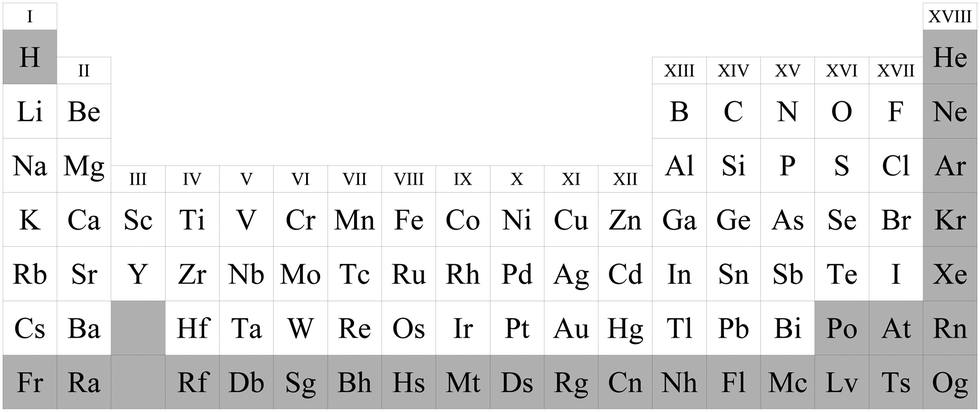 | ||
| Fig. 1 Periodic table. The uncolored 62 elements were used for our high-throughput calculations. | ||
Three types of 2 × 2 supercell AB2 structures (1T, 1H, and planar) as shown in Fig. 2 were prepared for each compound as its initial structures. Here, we note that the name of the 1T structure varies like trigonal, octahedral, CdI2-type, P![[3 with combining macron]](https://www.rsc.org/images/entities/char_0033_0304.gif) m1 (164), and D33d,67,79 while the name of the 1H structure varies like hexagonal, trigonal prismatic, MoS2-type, P
m1 (164), and D33d,67,79 while the name of the 1H structure varies like hexagonal, trigonal prismatic, MoS2-type, P![[6 with combining macron]](https://www.rsc.org/images/entities/char_0036_0304.gif) m2 (187), and D13h in the literature.67,79 We made the initial structures include fluctuation from −0.05 Å to 0.05 Å with respect to the ideal structures for atomic coordinates. To confirm the kinds of compounds that possess spin-polarized states, initial spin configurations were prepared as ferromagnetic spin states whose initial spin density is generated by a superposition of atomic charge density with biased populations of up and down spin charge densities of each atom. The length of the initial lattice vectors a was prepared on the basis of their atomic radii80RA and RB as
m2 (187), and D13h in the literature.67,79 We made the initial structures include fluctuation from −0.05 Å to 0.05 Å with respect to the ideal structures for atomic coordinates. To confirm the kinds of compounds that possess spin-polarized states, initial spin configurations were prepared as ferromagnetic spin states whose initial spin density is generated by a superposition of atomic charge density with biased populations of up and down spin charge densities of each atom. The length of the initial lattice vectors a was prepared on the basis of their atomic radii80RA and RB as 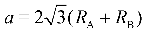 . The periodic slab approach with a vacuum layer of 15 Å was used to avoid interaction between periodic layers.
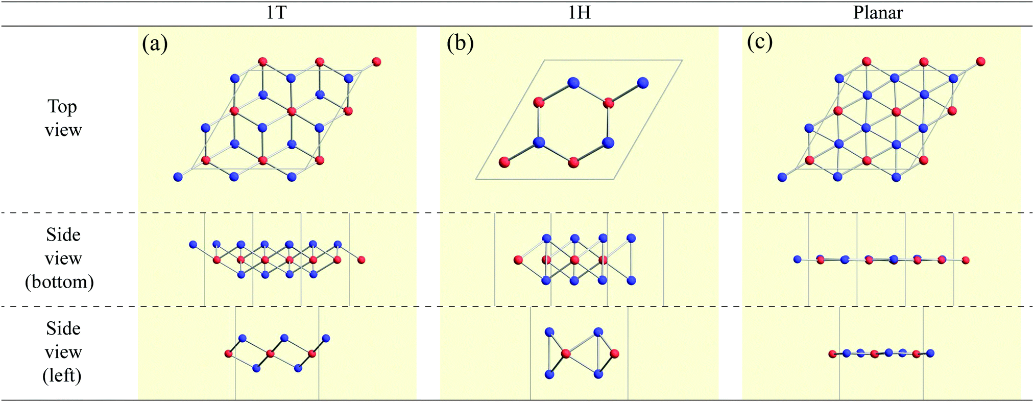 | ||
| Fig. 2 Top and side views of the initial structures of (a) 1T, (b) 1H, and (c) planar. Red and blue spheres represent atoms A and B, respectively, where there are 4 atoms of species A and 8 atoms of species B in the unit cell. | ||
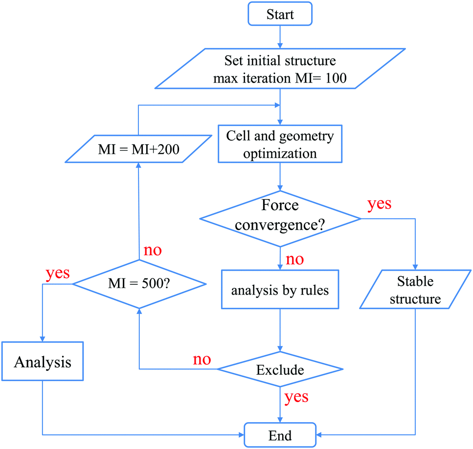
After reaching 100 iterations for the geometry optimization, we applied the following 5 conditional branch rules as illustrated in Fig. 3.
 | ||
| Fig. 3 The workflow based on the five conditional branch rules used to perform the cell and geometry optimizations for the structure map construction. | ||
(1) If all the geometry optimizations for three initial structures converge normally, the calculations are stopped, since stable structures have already been obtained.
(2) If at least one of the three calculations does not converge, and all the final structures are found to be in an amorphous structure, whose definition will be discussed later on, then the calculations are stopped, and the most stable structure is considered to be amorphous.
(3) If only one calculation does not converge, and this final structure is an amorphous structure which has the lowest energy, then the calculations are stopped, and the most stable structure is considered to be amorphous.
(4) If only one calculation converges, and this final structure has the highest energy while structures of the other two calculations are amorphous, then the calculations are stopped, and the most stable structure is considered to be amorphous.
(5) Otherwise, since the most stable structure cannot be determined, more geometry optimizations are performed until it reaches another 200 iterations, and we apply the above rules again. If it has already reached 500 iterations in total, the calculations are stopped, since it is hard to obtain the most stable structure.
Here, we categorized the final structures into planar, distorted planar, memory, 1![[scr T, script letter T]](https://www.rsc.org/images/entities/char_e533.gif) /1
/1![[script letter H]](https://www.rsc.org/images/entities/char_e142.gif) , and amorphous as shown in Fig. 4. The details of the definitions of these structures such as the tolerance we used are given in the caption of Fig. 4. All the structural figures in this paper are depicted using Crystallica.81,82 Here, we briefly explain the definition of the categorized structures. The group “planar” means that atoms B form almost flat honeycomb structures, and atoms A are on the center of the honeycombs. The group “distorted planar” means that the structures are distorted in the plane from the planar structure, while keeping the planarity with a tolerance. The group “memory” is defined as a group of structures which are similar to the planar, but the atoms A are shifted from the plane formed by atoms B. As we will discuss the memory structure later on, the position of the atom A is bistable, meaning that the atom A is stabilized either above or below the plane formed by the atoms B. Since the bistability in the position of the atom A might be utilized as binary digits, we call the buckled structure “memory structure”, which is expected to be a candidate material for data storage application with an extremely high areal density. In the other cases, judging from whether the top view of the structure is honeycomb-like, we classify the structure into the group “1/1” or the group “amorphous”. Specifically, if the variation in the distances between the first neighbouring atoms is smaller than 0.15 Å, the structures are categorized into the group “1/1”; otherwise, they are categorized into the group “amorphous”. Here, we use “1/1” instead of “1T/1H”, because the space-group symmetries of structures in 1/1 can be different from the original symmetry of 1T/1H (Pm1 (164)/Pm2 (187)), and 1/1 can include not only 1T/1H but also other characteristic structures.
, and amorphous as shown in Fig. 4. The details of the definitions of these structures such as the tolerance we used are given in the caption of Fig. 4. All the structural figures in this paper are depicted using Crystallica.81,82 Here, we briefly explain the definition of the categorized structures. The group “planar” means that atoms B form almost flat honeycomb structures, and atoms A are on the center of the honeycombs. The group “distorted planar” means that the structures are distorted in the plane from the planar structure, while keeping the planarity with a tolerance. The group “memory” is defined as a group of structures which are similar to the planar, but the atoms A are shifted from the plane formed by atoms B. As we will discuss the memory structure later on, the position of the atom A is bistable, meaning that the atom A is stabilized either above or below the plane formed by the atoms B. Since the bistability in the position of the atom A might be utilized as binary digits, we call the buckled structure “memory structure”, which is expected to be a candidate material for data storage application with an extremely high areal density. In the other cases, judging from whether the top view of the structure is honeycomb-like, we classify the structure into the group “1/1” or the group “amorphous”. Specifically, if the variation in the distances between the first neighbouring atoms is smaller than 0.15 Å, the structures are categorized into the group “1/1”; otherwise, they are categorized into the group “amorphous”. Here, we use “1/1” instead of “1T/1H”, because the space-group symmetries of structures in 1/1 can be different from the original symmetry of 1T/1H (Pm1 (164)/Pm2 (187)), and 1/1 can include not only 1T/1H but also other characteristic structures.
 | ||
| Fig. 4 Classification of final structures. Top and side views of examples of final structures for (a) 1T, (b) 1H, (c) planar,† (d) distorted planar,†† (e) memory,§ and (f) amorphous. † The difference of the length of each side of the honeycomb is smaller than 0.05 Å. In addition, 55° < ∠B1AB2 < 65°, where B1 and B2 are neighbouring atoms which are the first neighbouring atoms from atom A. The height of each atom from the average height of atoms is smaller than 0.05 Å. †† The difference in the length of each side of the honeycomb is smaller than 0.15 Å. In addition, the height of each atom from the average height of atoms is smaller than 0.15 Å. § The height of each atom from the average height of atoms is smaller than 0.2 Å. In addition, the height of each atom A from the plane formed by atoms B is larger than 0.5 Å. | ||
In this study, we restricted our attention only to constructing a structure map for almost all the AB2 compounds using high-throughput DFT calculations to search for possible 2D structures which have the potential to be 1T, 1H, planar, or memory structures. The structure map will give us an encompassing perspective on 2D structures of AB2 type compounds, and promote further detailed studies such as finite temperature molecular dynamics and phonon calculations to critically validate the structural stability of each newly found compound.
3 Results
3.1 Structure map of AB2 type monolayers
Based on the classification shown in Fig. 4, the most stable converged structures are summarized as a structure map for AB2 type monolayers in Fig. 5. 2332 compounds out of 3844 compounds in total were excluded as amorphous structures using the conditional branch rules no. 2–4, leading to 1512 compounds remaining. Since, among the 1512 compounds, it was hard to obtain the most stable structures for 214 compounds, whose calculations were terminated after 500 iterations using the conditional branch rule no. 5, they were classified into the group “unknown”. Lastly, we have the 1298 screened compounds, and called them “three stable structures” in this paper, since all three stable structures for these compounds were obtained using calculations which were performed from three initial structures: 1T, 1H, and planar. These 1298 compounds were further classified into planar, distorted planar, memory, 1/1, and amorphous.
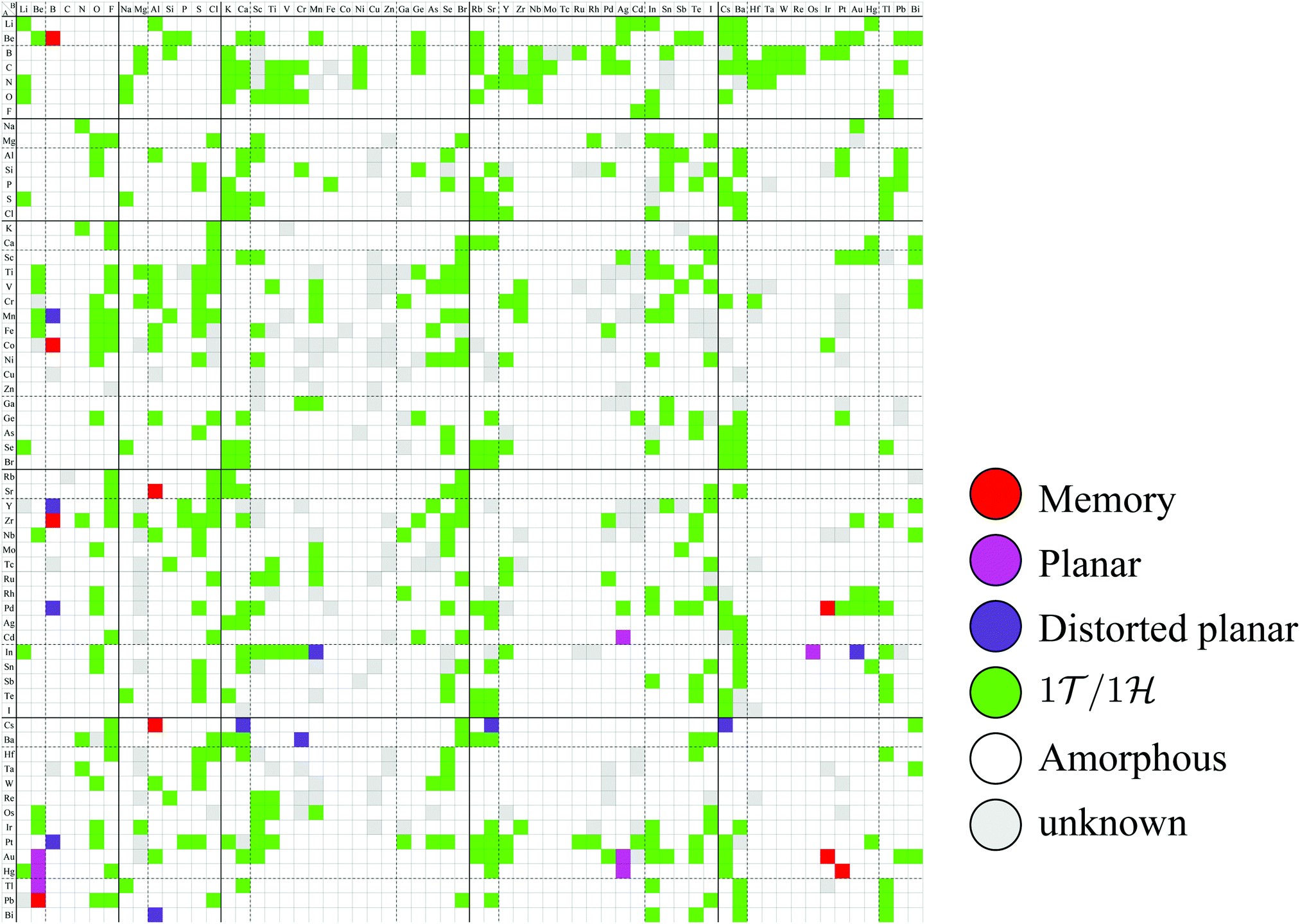 | ||
| Fig. 5 Structure map for AB2 type monolayers. The species of atom A and atom B are specified by the row and column, respectively. The color of each cell represents the obtained final structure, whose definitions are given in Fig. 4. | ||
In Fig. 5, the planar structures include Be, Ag, or Os as the atom B, while the memory structures include Be, B, Al, Ir, or Pt as the atom B. However, we could not find any other rules to be the planar or memory structures. In our DFT calculations, it was difficult to obtain stable structures for CuX2, XCu2, ZnX2, and XZn2, and almost all XM2 (M = Fe, Co, Ni, Cu, Zn, Nb, Mo, Tc, Ru, Rh, Ta, W, Re, and Os; X = arbitrary elements) compounds due to their slow convergence or preference for amorphous structures. This makes the shape of the distribution of the 1/1 structures sparse and striped.
3.2 Space-group classification
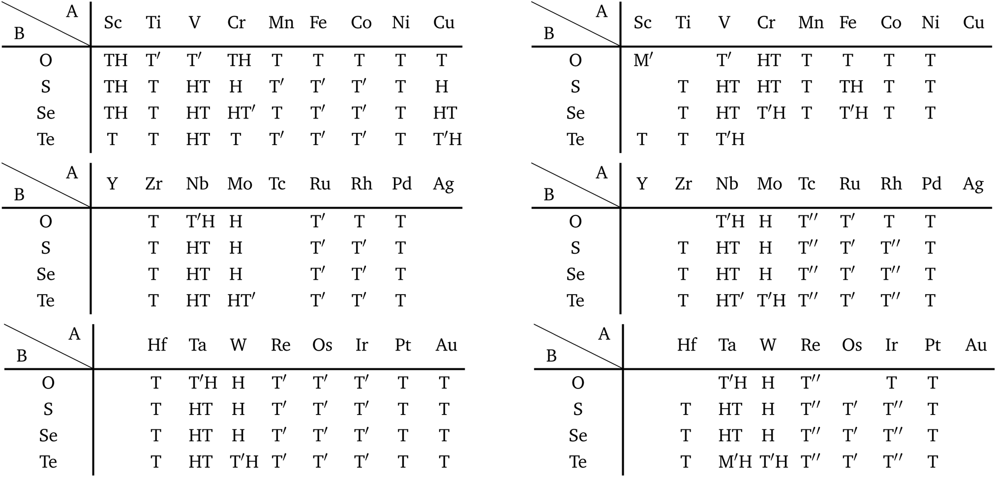
Although the rough screening method discussed above is useful to classify the most stable structures intuitively, it is not sufficient to understand the classification of complicated structures. For a more detailed discussion, we classified the structures of 1298 compounds in the group “three stable structures” by an analysis based on space-group. Their space-groups, which were searched using a program code Spglib83 with a distance tolerance of 0.5 Å,84 are summarized in Fig. 6. Since most of the 2D materials are not ideal planar structures, which can be treated by a 2D space-group, the rotation axis with the highest symmetry does not necessarily point in the direction normal to the layer. The structure map is also provided as an interactive website85 linked with a customized version of OpenMX Viewer,86 which enables us to easily visualize the obtained structures. The 1T (e.g. TiS2) and 1H (e.g. MoS2) phases correspond to the space-groups Pm1 (164) and Pm2 (187), respectively. Planar and distorted planar structures belong to P6/mmm (191) or Cmmm (65). In addition, in the structure map of Fig. 6, we set an acceptable energy range of 0.03 hartree (≈0.82 eV) per unit cell including 12 atoms for comparison among structures obtained from three initial states to consider the fact that the 2D materials can exist as metastable structures in real experiments due to their fabrication processes and interactions with substrates. The acceptable energy range was chosen properly to make the DFT results cover the experimental ones. This is mentioned later in Table 2 in the following Section 3.3.1. Therefore, the structure map does not show the space-groups of structures which are excluded due to the above acceptable energy even if the structures are in the group “three stable structures”.
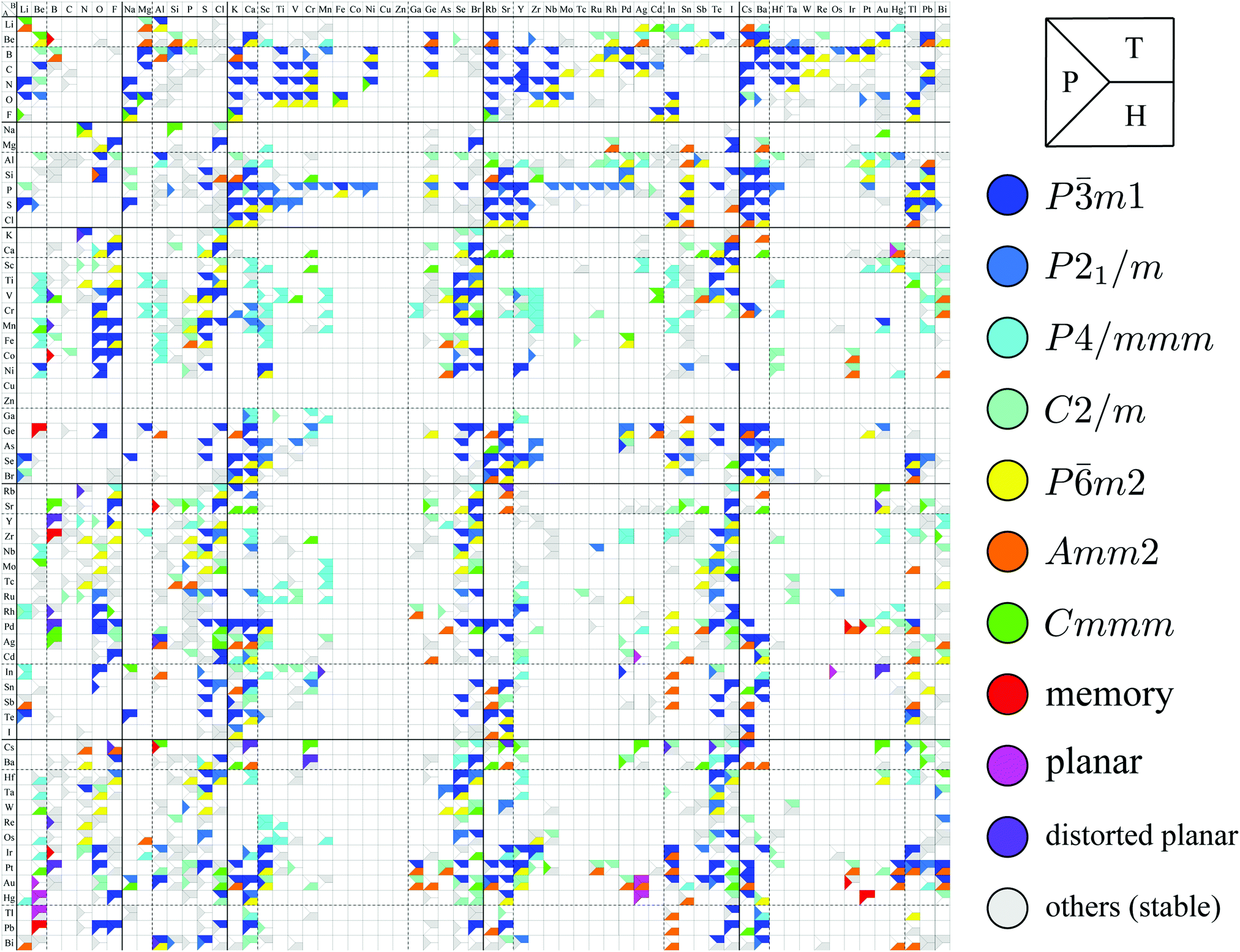 | ||
| Fig. 6 Space-group classification. The species of atom A and atom B are specified by the row and column, respectively. The upper, lower and left parts of each cell represent the initial structures 1T (T), 1H (H), and planar (P) in Fig. 2. The color of each part of the cell represents the obtained final structure's space-group. Each cell can have more than one colored part due to the acceptable energy range of 0.03 hartree (≈0.82 eV) per unit cell including 12 atoms. | ||
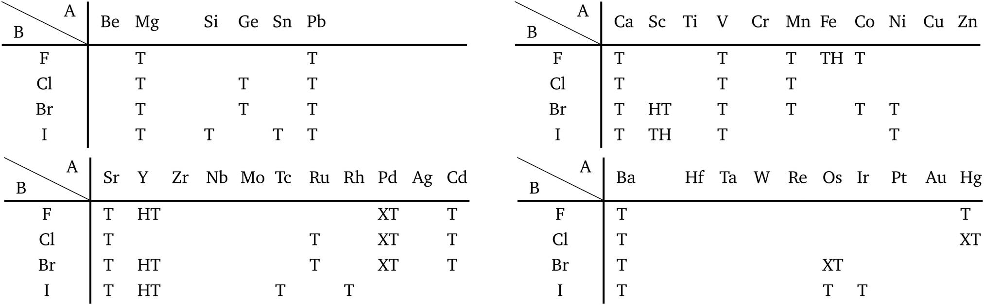
In Fig. 6, roughly speaking, most of the 1T structures can be found in TMDCs and TMDOs, metal dihalides, dialkali-metal materials including groups XIV, XV, XVI (chalcogenides/oxides), and XVII (halides) compounds, dialkaline-earth-metal materials including groups XIV, XV, XVI (chalcogenides/oxides), and XVII (halides) compounds, transition metal carbides/nitrides (MXenes) and borides/oxides, and some alloys. The names of the compounds’ with the 1T (Pm1) structures are summarized in Appendix B.1. Similarly, most of the 1H structures can be found in mono-metal compounds including diatoms in groups XV, XVI (chalcogenides), and XVII (halides), dialkali-metal and dialkaline-earth-metal materials including groups XVI (chalcogenides) and XVII (halides) compounds, transition metal carbides/nitrides (BiXenes) and borides/oxides, and some alloys. The names of the compounds with the 1H (Pm2) structures are summarized in Appendix B.5. The details of the families of 1T/1H structures are discussed in Section 3.3.4.
Besides the groups of 1T/1H, many structures in the space-group P4/mmm (123), which are composed of three square lattice layers, can be found in Fig. 6 especially in alloys as listed in Appendix B.3. Their structures are similar to the AB type structures such as FeSe87 which have a 4-fold rotational symmetry. Although we do not discuss the P4/mmm structure in detail, the P4/mmm structure might be an interesting family for the future 2D materials search.
In the following subsections, we discuss the obtained 1T/1H (TMDCs and TMDOs, metal dihalides, MXenes/BiXenes, and other 1T/1H), planar and distorted planar structures, memory structures, and other characteristic structures in detail.
3.3 1T/1H structures
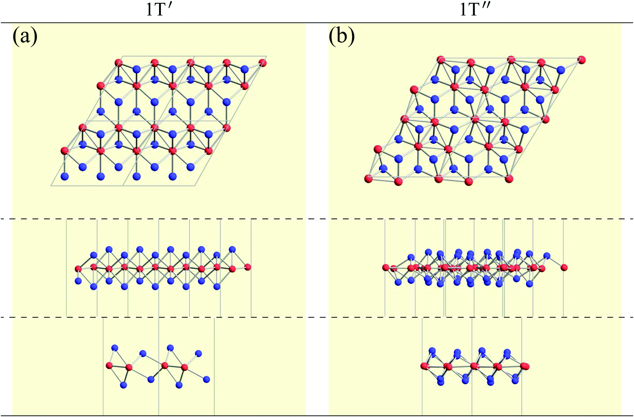
![[1 with combining macron]](https://www.rsc.org/images/entities/char_0031_0304.gif) or C2/m. It is noted that even when a structure belongs to P or C2/m, it is possible to form a different structure from 1T′′.
or C2/m. It is noted that even when a structure belongs to P or C2/m, it is possible to form a different structure from 1T′′.
 | ||
| Fig. 7 Top and side views of (a) 1T′ and (b) 1T′′ structures. | ||
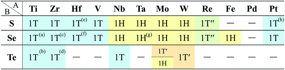
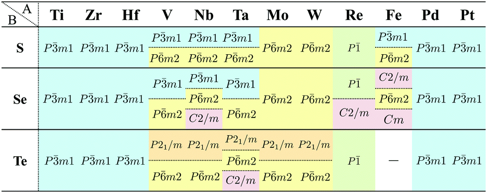
Our DFT results corresponding to Table 1 are shown in Table 2. Although our calculations do not include any interactions with a substrate, our DFT results are in good agreement with the experimental one. Other comparisons with previously reported DFT results of TMDCs and TMDOs are summarized in Tables 3–5. Most of our results are in good agreement with those of the other research groups, although structures which are in magnetic states such as materials including vanadium give different stable structures due to the initial spin configuration. Remember that we chose a ferromagnetic spin state as the initial spin configuration for all the compounds. The spin magnetic moment for each compound is shown in Appendix C. Tables 3–5 indicate that groups V and VI such as V, Nb, Ta, Cr, Mo, and W tend to form 1H, while groups IV and X such as Ti, Zr, Hf, Ni, Pd, and Pt tend to form 1T. This tendency is consistent with the 3D crystal structures of the TMDCs in groups IV, V, VI, VII, and X, which are known as well-defined layered structures.96
m1, Pm2, P21/m and P, respectively. Since we allowed the compounds to have multiple stable states by the acceptable energy range of 0.03 hartree (≈0.82 eV) per unit cell, all the acceptable structure symmetries are shown in the table. The acceptable energy range is chosen properly to make the DFT results cover the experimental ones
|
|
|
|
As for TMDOs, CoO2,49 MnO2,50 and RuO251 are experimentally known as the 1T intercalated layered structures. Our results indicate that monolayers of CoO2, MnO2, and RuO2 are 1T, 1T, and 1T′, respectively. This supports that the structures of intercalated layered materials are similar to their monolayers. Therefore, our analysis on monolayers can contribute to the prediction of new intercalated layered structures.
We additionally confirmed the stability of 164 converged TMDCs and TMDOs by using the finite temperature molecular dynamics simulation, which was performed with 1 femtosecond time step for 0.3 picoseconds at 1000 K. Our results showed that only three structures, AuO2-1H, AuSe2-1T and AuTe2-1T, dissociated. “-1T(1H)” means the initial structure is 1T(1H). However, the other 161 structures kept their stable structures. The results support the sufficient reliability of our database to provide comprehensive structural trends of the AB2 type compounds in 2D structures.
In this subsection, we focus on only transition metals for discussion of dichalcogenides and dioxides. However, it is noteworthy that alkaline-earth-metal materials such as BeTe2, MgO2, CaO2, CaS2, CaSe2, CaTe2, SrSe2, and BaS2 also prefer the 1T/1H structure according to the structure map of Fig. 6.
Most transition metal dihalide layered structures are known as the CdI2 (Pm1) type or CdCl2 (Rm) type structure, whose monolayer has 1T symmetry (see ref. 97 and references therein). Structures obtained by our calculations are shown in Table 6. Almost all the monolayer transition dihalides prefer the 1T structure. The families including the Y atom prefer the 1H structure though energetically the 1T structure is allowable, while ScBr2, ScI2, and FeF2 can also have the 1H structure.
|
Apart from transition metal dihalides, Fig. 6 indicates that dihalides including group II, XII or XIV elements also prefer the 1T structure. It is noteworthy that some of the dihalide 3D crystal structures including group II or XII elements such as MgCl2, MgBr2, MgI2, CaI2, and CdBr2 are also known as the CdI2 (Pm1) type or CdCl2 (Rm) type structure.102,103
|
|
The group TM-XV includes 15 1H structures. Transition metal dinitrides in TM-XV such as MoN2,112 ReN2,113 OsN2,114 IrN2,114,115 and PtN2115 are known as multilayered MoS2 type structures (1H). However, only ReN2 and OsN2 out of them can have the 1H structure in our calculations. This implies that these multilayers strongly interact with each other in their crystals. Our calculation also indicates that TiN2, ZrN2, and TcN2 can have the 1H structure. Here, we note that a different structure type, M-phase, has been reported for group V transition metal dinitrides (TaN2, NbN2, and VN2) by using DFT calculations.116 However, we could not obtain these structures due to the limitation of our choice of initial structures.
According to ref. 117, DFT calculations have predicted that dialkali-metal monochalcogenides (group XVI) are 1T-phase semiconductors, which have the inherent layer-by-layer structure with very weak interlayer coupling. It is found in Table 8 that not only dialkali-metal monochalcogenides (XVI-I), but also dialkali-metals and dialkaline-earth-metals materials including groups XIV, XV, XVI (chalcogenides/oxides), and XVII (halides) compounds, namely XIV-I, XV-I, XVII-I, XIV-II, XV-II, XVI-II, and XVII-II such as compounds listed in Appendix E.1 can have the 1T symmetry. In addition, dialkali-metals halides, dialkaline-earth-metals chalcogenides/oxides, and dialkaline-earth-metals halides, namely XVII-I, XVI-II, and XVII-II such as the compounds listed in Appendix E.2 can have the 1H symmetry in our calculations. Therefore, these huge families of dialkali-metals and dialkaline-earth-metals materials are good candidates for new 2D materials, which may have a variety of electronic, magnetic, and optical properties.
Other 1T structures are found in ditransition metal mono-borides/oxides, namely XIII-TM and XVI-TM such as BTi2, BNi2, BY2, BNb2, BPd2, BHf2, BTa2, BW2, BIr2, BPt2, OSc2, OTi2, OV2, OCr2, OFe2, and ONb2, other ditransition metals such as XIV-TM and XV-TM, dichalcogenides/dioxides and dihalides such as XIV-XVI, XV-XVI, XVI-XVI, XII-XVII, and XIV-XVII, alloys, namely TM-I, TM-II, and TM-TM, and the other 1T families such as TM-XIII, XVI-XIII, and XVII-XIII, while the other 1H structures are found in ditransition metal mono-borides/oxides, namely XIII-TM and XVI-TM such as BNi2, BRu2, BRh2, BPd2, BW2, BRe2, BIr2, BPt2, OTi2, OV2, OCr2, OFe2, OZr2, and ONb2, other ditransition metals such as XIV-TM, alloys, namely TM-TM, and the other 1H families such as TM-XV, XII-II, II-XVI, XVI-XIII and XIV-XIV. Again, the specific names of the 1T/1H structures for each combination of groups are listed in Appendix E. As we mentioned in Section 3.2, all the 1T and 1H structures we obtained are listed in Appendices B.1 and B.5.
3.4 Planar and distorted planar structures
The graphene and h-BN are well-known as planar honeycomb monolayers. As for AB2 type structures, Cu2S, Cu2Si, and Ag2Bi synthesized on a substrate are experimentally known as flat structures.3 However, the stable structures of these compounds could not be obtained in our calculations, since they are always strongly coupled with a substrate in experiments. From the structure map of Fig. 5, we predicted that 18 compounds can be planar or distorted planar structures (7 planar structures, such as CdAg2, InOs2, AuBe2, AuAg2, HgBe2, HgAg2, and TlBe2, and 11 distorted planar structures such as MnB2, YB2, PdB2, InMn2, InAu2, CsCa2, CsSr2, CsCs2, BaCr2, PtB2, and BiAl2).Assuming the acceptable energy range of 0.03 hartree per unit cell, as in Fig. 6, 30 compounds can be planar or distorted planar structures (8 planar structures, such as CaHg2, CdAg2, InOs2, AuBe2, AuA2g2, HgBe2, HgAg2, and TlBe2, and 22 distorted planar structures, such as KN2, VB2, MnB2, RbN2, RbSr2, SrAu2, YB2, RhB2, PdB2, AgAl2, InMn2, InAu2, CsF2, CsCa2, CsSr2, CsIn2, CsTe2, CsCs2, BaCr2, ReB2, PtB2, and BiAl2). Moreover, assuming that the threshold of the height, which is the distance between the highest atom and the lowest atom in a direction vertical to the monolayer, is set to be 0.5 Å, the number of planar-like structures is found to be 74 as listed in Appendix B.10.
3.5 Memory structures
In the structure map of Fig. 5, we predicted that 9 structures (AuIr2, BeB2, CoB2, CsAl2, HgPt2, PbBe2, PdIr2, SrAl2, and ZrB2) can be memory structures. As we mentioned in Section 2, the memory structure is a structure in which atoms A are above the center of almost flat honeycomb structures formed by atoms B. Therefore, positions (up or down) of atoms A can represent binary digits. As the primitive cell of SrAl2, whose lattice constant and area are 4.60 Å and 1.83 mm2, includes only one Sr atom as atom A, the areal density for the storage application is 5.46 × 1012 bit per mm2, while the areal density of the present HDD storage is about 109 bit per mm2.118,119 We performed the nudged elastic band (NEB) calculations120 for these memory structures to confirm whether it is possible to control each of them nearly independently with a proper energy barrier in considering binary digit storage applications. The NEB calculation for SrAl2 is shown in Fig. 9. About 2.2 eV energy barriers of SrAl2 are enough to use it for binary digit storage applications at room temperature, as, for example, the AFM tip can be controlled within the accuracy of less than 1 eV Å−1.26 We also confirmed the stability by using the finite temperature molecular dynamics simulation, which was performed with 1 femtosecond time step for 3 picoseconds at 1000 K, to ensure that the structure does not dissociate. Therefore, it is concluded that SrAl2 is an admirable candidate for a new binary digit storage application. The NEB results for the other memory structures are shown in Appendix F. Since AuIr2, PdIr2, and HgPt2 have 0.2–0.8 eV energy barriers, they are also candidates for memory devices. The energy barriers are related to the stability of a structure in which atoms A are in the same side. In addition, the energy barriers are also related to the ease in which an atom A can penetrate the honeycomb hole of atoms B. Therefore, although BeB2, CsAl2, and PbBe2 belong to a memory structure, their energy barriers are too low to control the structures for binary digit storage applications due to their distorted structures and ease of penetration. For example, since the lattice constants of CsAl2 are much larger than those of the other memory structures as the relative size of the sphere of the atoms in the panels in Fig. 8 suggests, the energy barrier is low. The structures of CoB2 and ZrB2 are too unstable to obtain NEB results, as the height of protrusive atoms in these materials is much lower than that of the other memory structures.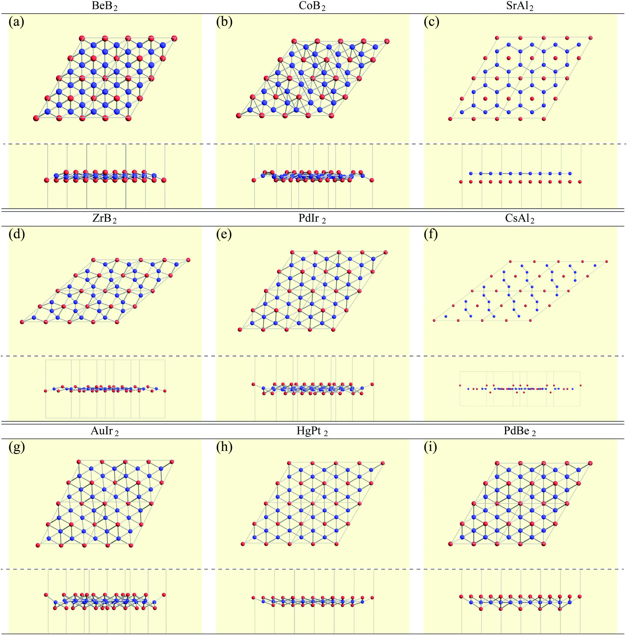 | ||
| Fig. 8 Top and side views of 9 memory structures. | ||
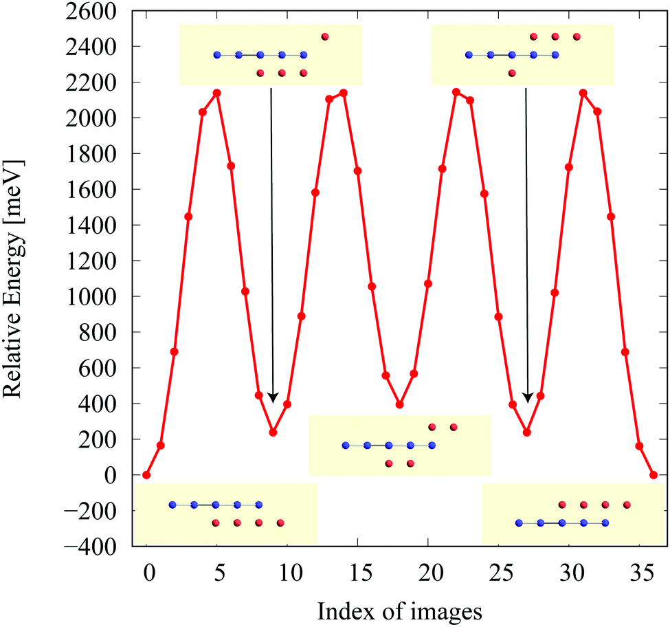 | ||
| Fig. 9 The NEB result for the SrAl2 memory structure. The five structures on the local minima were prepared to represent a model of a binary digit storage application. Each minimum energy path between two of them is obtained by optimizing 8 images on the path. The whole energy path is obtained by connecting all the minimum energy paths. The corresponding geometrical structures of images on the local energy minima are depicted in the figure. | ||
Assuming that the threshold of the height, which is the distance between the highest atom and the lowest atom in a direction vertical to the monolayer, is set to be 0.5 Å and non-honeycomb structures are allowed with the acceptable energy range of 0.03 hartree per unit cell as in Fig. 6, the number of memory-like structures is found to be 24 as listed in Appendix B.12.
3.6 Characteristic structures
Finally, we pick up some characteristic structures which have a minor space-group symmetry. Their structures are shown in Fig. 10. PtPb2 in P (174) symmetry has a 6-fold rotational symmetry and Pt atoms are in the same plane. WN2 in P3 (143) symmetry is similar to the 1T structure, but the W atoms are buckled. GeC2 in P![[4 with combining macron]](https://www.rsc.org/images/entities/char_0034_0304.gif) 21m (113) symmetry is a buckled pentagonal planar structure, which is similar to the penta-monolayers in ref. 121 and references therein. As for BAu2 with P4/mbm (127) symmetry and SAu2 with P4212 (90) symmetry, Au atoms form an isogonal distorted square arrangement. While boron atoms are on the Au plane, S atoms are above the Au plane similar to the memory structures. Both of them are pentagonal monolayers. In SnBe2 in Pma2 (28) symmetry, Sn atoms are distributed above and below the plane of a buckled trigonal lattice Be monolayer. Structures of ScO2 in C2/m (12) symmetry and TaTe2 in C2/m (12) symmetry can be viewed as mixtures of 1T and 1H structures from the top view. This kind of mixed structure is referred in ref. 116 as the M-phase. However, the structures of ScO2 and TaTe2 are little different from the M-phase in terms of a boundary structure between 1T and 1H. Therefore, we called them M′-phase in Tables 3 and 5. BeHf2 in P4mm (99) symmetry, which looks like a series of baskets, has a 4-fold rotational symmetry. PBe2 in P3m1 (156) symmetry is one of the most interesting structures. The first layer is formed by a buckled honeycomb structure of P and Be atoms. The second layer is a kagome lattice of Be atoms. The rest of the P atoms are above the center of the hexagons of the kagome lattice. In HgGe2 with P3m1 (156) symmetry, Ge atoms form germanene, and Hg atoms are above the center of the hexagons as memory structures. CTl2 in P3m1 (156) symmetry is similar to HgGe2, but C and Tl atoms form a buckled honeycomb structure.
21m (113) symmetry is a buckled pentagonal planar structure, which is similar to the penta-monolayers in ref. 121 and references therein. As for BAu2 with P4/mbm (127) symmetry and SAu2 with P4212 (90) symmetry, Au atoms form an isogonal distorted square arrangement. While boron atoms are on the Au plane, S atoms are above the Au plane similar to the memory structures. Both of them are pentagonal monolayers. In SnBe2 in Pma2 (28) symmetry, Sn atoms are distributed above and below the plane of a buckled trigonal lattice Be monolayer. Structures of ScO2 in C2/m (12) symmetry and TaTe2 in C2/m (12) symmetry can be viewed as mixtures of 1T and 1H structures from the top view. This kind of mixed structure is referred in ref. 116 as the M-phase. However, the structures of ScO2 and TaTe2 are little different from the M-phase in terms of a boundary structure between 1T and 1H. Therefore, we called them M′-phase in Tables 3 and 5. BeHf2 in P4mm (99) symmetry, which looks like a series of baskets, has a 4-fold rotational symmetry. PBe2 in P3m1 (156) symmetry is one of the most interesting structures. The first layer is formed by a buckled honeycomb structure of P and Be atoms. The second layer is a kagome lattice of Be atoms. The rest of the P atoms are above the center of the hexagons of the kagome lattice. In HgGe2 with P3m1 (156) symmetry, Ge atoms form germanene, and Hg atoms are above the center of the hexagons as memory structures. CTl2 in P3m1 (156) symmetry is similar to HgGe2, but C and Tl atoms form a buckled honeycomb structure.
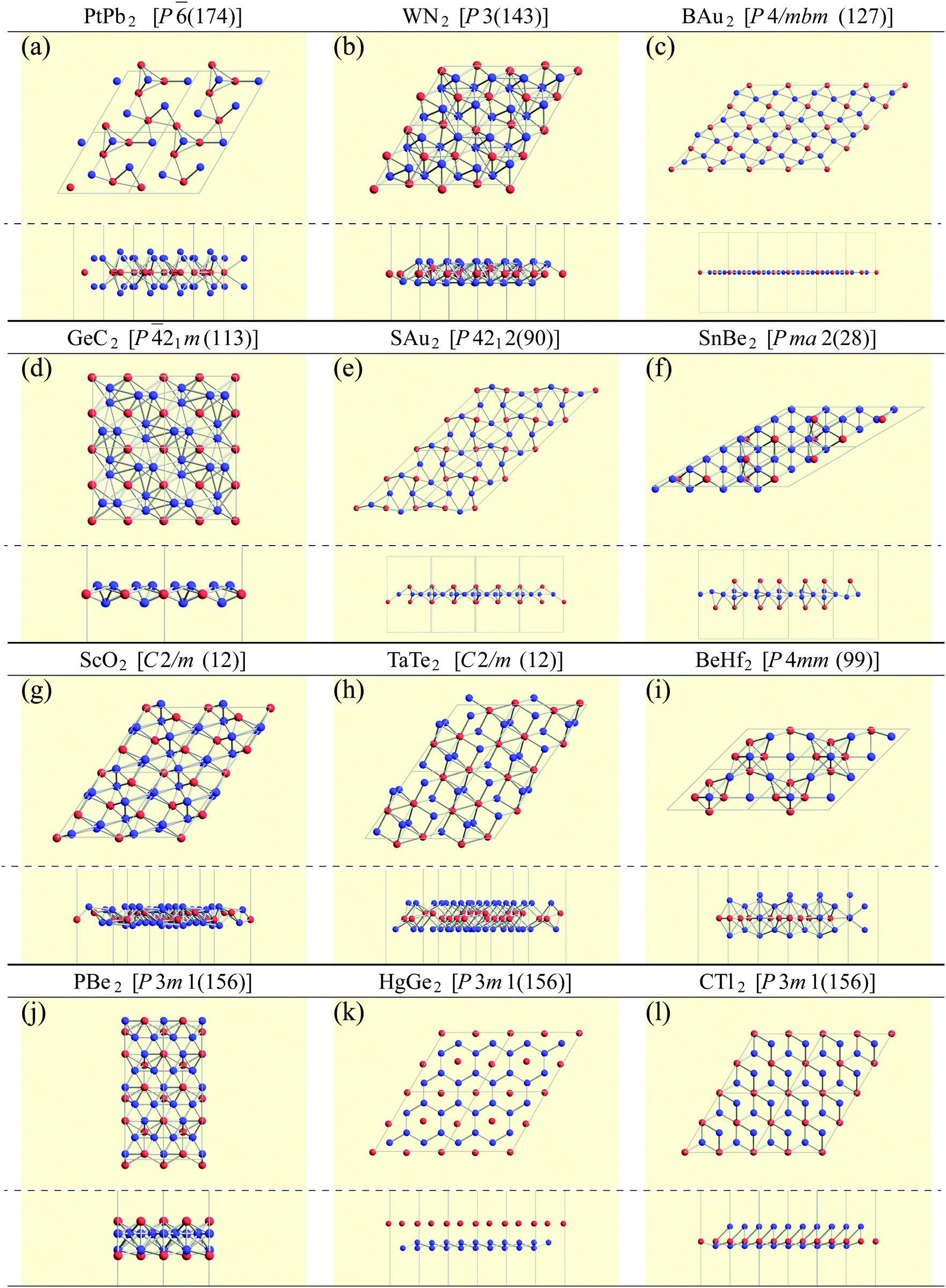 | ||
| Fig. 10 Top and side views of characteristic structures. | ||
4 Conclusions
In this paper, we have constructed a structure map for AB2 type 2D materials as shown in Fig. 5 on the basis of high-throughput DFT calculations by starting from the initial structures: 1T, 1H, and planar structures. The obtained structures have been classified by their space-group as shown in Fig. 6. The compounds in the major space-groups are listed in Appendix B. The figures of the structures and lattice parameters we obtained are given in the ESI† S1–S4. Furthermore, our structure map and database are available on the interactive website85 linked with a customized version of OpenMX Viewer,86 which enables us to easily visualize the obtained structures. The density of states and the band structures are also available on the interactive website.Our results of the well-known families of the 1T/1H (Pm1/Pm2) structures, such as
• TMDCs and TMDOs shown in Tables 1–5 in Section 3.3.1
• metal dihalides shown in Table 6 in Section 3.3.2
• MXenes and BiXenes shown in Table 7 in Section 3.3.3,
have been compared with the experimental data and previously reported DFT calculations to confirm the reliability of our structure map. The results of the finite temperature molecular dynamics simulations for the TMDCs and TMDOs also support the sufficient reliability of our structure map generated using symmetry-unconstrained calculations, although we have not confirmed the stability of all the compounds by using the molecular dynamics simulations.
We have summarized the families of the 1T/1H structures as shown in Table 8 in Section 3.3.4. The left side of Table 8 has predicted that most of the 1T structures can be found in the following families:
• TMDCs and TMDOs (TM-XVI).
• metal dihalides (II-XVII, and TM-XVII).
• other dichalcogenides/dioxides and dihalides such as XIV-XVI, XV-XVI, XVI-XVI, XII-XVII, and XIV-XVII.
• MXenes and others in XIV-TM and XV-TM.
• ditransition metals such as XIII-TM and XVI-TM.
• dialkali-metals such as XIV-I, XV-I, XVI-I, and XVII-I.
• dialkaline-earth-metals such as XIV-II, XV-II, XVI-II, and XVII-II.
• alloys such as TM-I, TM-II, and TM-TM.
• other 1T families such as TM-XIII, XVI-XIII, and XVII-XIII.
From the right-hand side of Table 8, it has been predicted that most of the 1H structures can be found in the following families:
• TMDCs and TMDOs (TM-XVI).
• alkaline-earth-metal dichalcogenides/oxides (II-XVI).
• metal dihalides (I-XVII and TM-XVII).
• BiXenes and others in XIV-TM.
• ditransition metal mono-borides/oxides and others in XIII-TM and XVI-TM.
• dialkali-metals halides, namely XVII-I.
• dialkaline-earth-metals chalcogenides and dialkaline-earth-metals halides, namely XVI-II and XVII-II.
• other dialkaline-earth-metals such as XII-II.
• alloys, namely TM-TM.
• other 1H families such as TM-XV, XVI-XIII, and XIV-XIV.
The names of the specific compounds of the 1T/1H structures for each combination of groups are given in Appendix E.
In addition, from the structure map of Fig. 5, we also predicted the following structures:
• 7 planar structures such as CdAg2, InOs2, AuBe2, AuAg2, HgBe2, HgAg2, and TlBe2,
• 11 distorted planar structures such as MnB2, YB2, PdB2, InMn2, InAu2, CsCa2, CsSr2, CsCs2, BaCr2, PtB2, and BiAl2,
• 9 memory structures such as AuIr2, BeB2, CoB2, CsAl2, HgPt2, PbBe2, PdIr2, SrAl2, and ZrB2,
Furthermore, the NEB calculations have been performed for memory structures as shown in Fig. 9 and 12. The NEB results have supported a possibility to control the memory structures (SrAl2, AuIr2, PdIr2, and HgPt2) for binary digit data storage applications.
We have also found other characteristic structures as shown in Fig. 10:
• the 6-fold rotational symmetry structure (PtPb2),
• pentagonal monolayers (GeC2, BAu2, and SAu2),
• a buckled trigonal lattice (SnBe2),
• mixed structures of the 1T and 1H structures (ScO2 and TaTe2),
• the 4-fold rotational symmetry structure (BeHf2),
• buckled honeycomb and kagome layers (PBe2),
• memory-like structures including germanene (HgGe2) and h-CTl (CTl2).
They can be new candidates for the AB2 type 2D materials. As we have mentioned in Section 3.2, the P4/mmm structures listed in Appendix B.3 are also an interesting family of 2D materials.
We expect that the structure map of AB2 type 2D materials we presented in this paper will give new viewpoints and directions to search unknown 2D materials for experimentalists, and promote further research to investigate the feasibility of newly found compounds and unveil their physical and chemical properties theoretically. Further research to construct structure maps for other compounds such as AB and AB3 types will be an important future direction to obtain a more comprehensive understanding of structural trends of 2D compounds and discover unknown 2D materials with a wide range of stoichiometric composition ratios.
Conflicts of interest
There are no conflicts to declare.A List of basis sets
The basis sets we used in this paper are listed in Table 9. For example, Fe6.0H-s3p2d1 means that three, two, and one optimized radial functions were allocated for the s, p, and d orbitals, respectively, for Fe atoms with the “hard” pseudopotential, and the cutoff radius of 6 bohr was chosen.| Li8.0-s3p2 | Fe6.0H-s3p2d1 | Cd7.0-s3p2d2 |
| Be7.0-s3p2 | Co6.0H-s3p2d1 | In7.0-s3p2d2 |
| B7.0-s2p2d1 | Ni6.0H-s3p2d1 | Sn7.0-s3p2d2 |
| C6.0-s2p2d1 | Cu6.0H-s3p2d1 | Sb7.0-s3p2d2 |
| N6.0-s2p2d1 | Zn6.0H-s3p2d1 | Te7.0-s3p2d2f1 |
| O6.0-s2p2d1 | Ga7.0-s3p2d2 | I7.0-s3p2d2f1 |
| F6.0-s2p2d1 | Ge7.0-s3p2d2 | Cs12.0-s3p2d2 |
| Na9.0-s3p2d1 | As7.0-s3p2d2 | Ba10.0-s3p2d2 |
| Mg9.0-s3p2d2 | Se7.0-s3p2d2 | Hf9.0-s3p2d2 |
| Al7.0-s2p2d1 | Br7.0-s3p2d2 | Ta7.0-s3p2d2 |
| Si7.0-s2p2d1 | Rb11.0-s3p2d2 | W7.0-s3p2d2 |
| P7.0-s2p2d1f1 | Sr10.0-s3p2d2 | Re7.0-s3p2d2 |
| S7.0-s2p2d1f1 | Y10.0-s3p2d2 | Os7.0-s3p2d2 |
| Cl7.0-s2p2d1f1 | Zr7.0-s3p2d2 | Ir7.0-s3p2d2 |
| K10.0-s3p2d1 | Nb7.0-s3p2d2 | Pt7.0-s3p2d2 |
| Ca9.0-s3p2d1 | Mo7.0-s3p2d2 | Au7.0-s3p2d2 |
| Sc9.0-s3p2d1 | Tc7.0-s3p2d2 | Hg8.0-s3p2d2f1 |
| Ti7.0-s3p2d1 | Ru7.0-s3p2d2 | Tl8.0-s3p2d2f1 |
| V6.0-s3p2d1 | Rh7.0-s3p2d2 | Pb8.0-s3p2d2f1 |
| Cr6.0-s3p2d1 | Pd7.0-s3p2d2 | Bi8.0-s3p2d2f1 |
| Mn6.0-s3p2d1 | Ag7.0-s3p2d2 |
B Structure classification
Compounds for each symmetry shown in Fig. 6 in Section 3.2 are listed in the following subsections.B.1
P![[3 with combining macron]](https://www.rsc.org/images/entities/h3_char_0033_0304.gif) m1 (164)
m1 (164)
LiAl2, BeCa2, BeGe2, BeRb2, BeTe2, BeCs2, BeBa2, BeAu2, BePb2, BMg2, BSi2, BK2, BTi2, BNi2, BGe2, BRb2, BY2, BNb2, BPd2, BSn2, BBa2, BHf2, BTa2, BW2, BIr2, BPt2, CBe2, CMg2, CK2, CCa2, CTi2, CV2, CCr2, CNi2, CGe2, CRb2, CY2, CNb2, CPd2, CAg2, CCs2, CBa2, CHf2, CTa2, CPb2, NLi2, NNa2, NK2, NCa2, NTi2, NV2, NCr2, NNi2, NRb2, NSr2, NY2, NZr2, NNb2, NCs2, NHf2, NTa2, NPb2, OLi2, ONa2, OMg2, OK2, OSc2, OTi2, OV2, OCr2, OFe2, ORb2, ONb2, OIn2, OCs2, OTl2, FNa2, FK2, FRb2, FCd2, FIn2, FTl2, NaN2, MgF2, MgCl2, MgBr2, MgI2, AlO2, AlAl2, SiO2, SiS2, SiCa2, SiSr2, SiI2, SiCs2, SiBa2, SiPb2, PS2, PK2, PCa2, PFe2, PSe2, PRb2, PSr2, PY2, PSn2, PTe2, PCs2, PBa2, PTl2, PPb2, SLi2, SNa2, SK2, SCa2, SSc2, SRb2, SSr2, SY2, SSn2, SCs2, SBa2, STl2, SPb2, ClK2, ClCa2, ClRb2, ClSr2, ClY2, ClIn2, ClCs2, ClBa2, ClTl2, KN2, CaF2, CaCl2, CaBr2, CaI2, ScBr2, ScTe2, ScI2, TiS2, TiSe2, TiTe2, VF2, VS2, VCl2, VSe2, VBr2, VI2, CrO2, CrSe2, CrCs2, MnO2, MnF2, MnS2, MnCl2, MnSe2, MnBr2, MnAu2, FeO2, FeF2, FeS2, CoO2, CoF2, CoBr2, NiBe2, NiO2, NiS2, NiSc2, NiSe2, NiBr2, NiY2, NiI2, GeO2, GeMg2, GeCl2, GeCa2, GeSe2, GeBr2, GeSr2, GeCd2, GeTe2, GeCs2, GeBa2, AsS2, AsCa2, AsSe2, AsSr2, AsPd2, AsSn2, AsTe2, AsCs2, AsBa2, SeLi2, SeNa2, SeS2, SeK2, SeCa2, SeSe2, SeRb2, SeSr2, SeY2, SeIn2, SeCs2, SeBa2, SeTl2, BrK2, BrCa2, BrRb2, BrSr2, BrCs2, BrBa2, BrTl2, RbK2, SrF2, SrCl2, SrBr2, SrI2, YF2, YBr2, YI2, ZrS2, ZrSe2, ZrTe2, NbS2, NbSe2, TcI2, RuCl2, RuBr2, RhO2, RhY2, RhI2, PdO2, PdF2, PdS2, PdCl2, PdK2, PdCa2, PdSc2, PdSe2, PdBr2, PdRb2, PdSr2, PdTe2, PdCs2, PdTl2, AgAl2, AgCa2, AgSr2, AgCs2, AgBa2, CdF2, CdCl2, CdBr2, CdBa2, InO2, InPd2, SnO2, SnS2, SnCa2, SnBr2, SnSr2, SnI2, SnBa2, SbS2, SbK2, SbSe2, SbTe2, SbBa2, TeLi2, TeNa2, TeS2, TeK2, TeSe2, TeRb2, TeSr2, TeTe2, TeCs2, TeTl2, ISr2, ICs2, CsCs2, BaF2, BaCl2, BaBr2, BaI2, HfS2, HfSe2, HfTe2, TaN2, TaS2, TaSe2, OsBr2, OsI2, IrO2, IrSc2, IrSr2, IrY2, IrZr2, IrIn2, IrI2, IrBa2, IrTl2, PtO2, PtS2, PtK2, PtSc2, PtGa2, PtSe2, PtRb2, PtSr2, PtY2, PtIn2, PtTe2, PtCs2, PtHg2, PtTl2, PtBi2, AuAl2, AuK2, AuCa2, AuSc2, AuSe2, AuRb2, AuSr2, AuIn2, AuSb2, AuTe2, AuCs2, AuHg2, AuBi2, HgF2, HgCl2, HgCa2, HgSr2, HgCs2, TlI2, PbO2, PbF2, PbCl2, PbCa2, PbBr2, PbSr2, PbI2, PbBa2, BiAl2, BiS2, BiTe2, BiBa2.
B.2 P21/m (11)
BeZr2, BeTa2, BSi2, BCr2, BMn2, BRh2, BOs2, CCd2, NPb2, OBe2, OZr2, OMo2, OBa2, OPt2, OAu2, AlSb2, AlHg2, SiPd2, SiCs2, PSi2, PSc2, PTi2, PV2, PCr2, PMn2, PCo2, PNi2, PGe2, PSr2, PNb2, PMo2, PTc2, PRu2, PRh2, PPd2, PHf2, PPt2, SBe2, STi2, SV2, SZr2, SPb2, SBi2, ClK2, TiCl2, TiBr2, VO2, VY2, VTe2, CrK2, CrCa2, CrSe2, CrBa2, MnCa2, MnSc2, CoSe2, CoZr2, NiSn2, GaCa2, GeCr2, GePd2, GeAu2, AsSc2, AsV2, AsSr2, AsZr2, AsBa2, AsHf2, SeLi2, SeSc2, SeY2, SeZr2, SeSn2, SePb2, BrLi2, BrK2, BrRb2, BrSn2, BrHf2, RbCa2, ZrCl2, ZrBr2, ZrI2, NbCa2, NbRu2, NbTe2, MoP2, MoTe2, RuO2, RuP2, RuS2, RuCa2, RuSe2, RuTe2, RuOs2, RhY2, CdCa2, InS2, InTe2, SnCl2, SnCr2, TeLi2, TeCa2, TeSc2, TeTl2, IK2, CsTl2, HfF2, HfCl2, HfBr2, HfI2, TaAs2, TaTe2, TaBi2, WP2, WSr2, WTe2, ReBi2, OsS2, OsSe2, OsTe2, IrAl2, IrCa2, IrSb2, PtTl2, PtPb2, AuNa2, AuRb2, AuTe2, HgCa2, TlBa2, BiSi2, BiS2, BiY2, BiBa2.B.3 P4/mmm (123)
LiIn2, LiSn2, LiBa2, LiHg2, BeSc2, BeMn2, BeAg2, MgSc2, AlAl2, AlCa2, AlSc2, AlY2, AlRh2, AlAg2, AlBa2, AlPt2, AlAu2, KCl2, KBr2, CaO2, CaS2, CaSe2, ScCa2, ScSc2, ScAg2, ScIn2, ScPt2, ScAu2, ScHg2, ScBi2, TiBe2, TiMg2, TiAl2, TiCa2, TiIn2, TiHf2, TiTl2, VBe2, VSc2, VTi2, VMn2, VY2, VZr2, VPb2, CrMg2, CrAl2, CrCa2, CrSc2, CrMn2, CrGa2, CrSr2, CrY2, CrZr2, CrSn2, CrHf2, MnBe2, MnCa2, MnSc2, MnMn2, MnZr2, MnIn2, MnAu2, MnPb2, FeBe2, FeAl2, FeSc2, CoAl2, NiBe2, NiHg2, GaCa2, GaCr2, GaMn2, GaY2, GeCr2, RbF2, RbCl2, RbBr2, RbI2, SrS2, YN2, YP2, YAs2, YBi2, ZrMg2, ZrCa2, ZrPd2, ZrIn2, ZrAu2, ZrTl2, NbBe2, MoMn2, TcTi2, TcMn2, TcY2, RuSc2, RuTi2, RuMn2, RuY2, RhLi2, RhAu2, RhHg2, PdAg2, AgSc2, CdK2, CdY2, InLi2, InCa2, InSc2, InCr2, InY2, InBa2, SnCa2, CsBr2, CsI2, BaS2, BaSe2, BaTe2, HfBe2, HfCa2, HfY2, HfTl2, TaBe2, TaY2, ReSc2, ReTi2, OsBe2, OsSc2, OsTi2, OsMn2, IrBe2, IrMg2, IrCa2, IrSr2, IrZr2, AuSn2, AuPb2, HgLi2, TlCa2, TlBa2.B.4 C2/m (12)
LiMg2, BeSi2, BeSe2, BeRu2, BeRh2, BeIn2, BeRe2, BBe2, BB2, BAl2, BP2, NBe2, OCs2, FRb2, NaCl2, MgRh2, MgBa2, AlBe2, AlF2, AlK2, AlGe2, AlSe2, AlRb2, AlRu2, AlRh2, AlPd2, AlAg2, AlBa2, AlHf2, AlIr2, AlAu2, SiNa2, SiZr2, SiPt2, SiPb2, PLi2, PNa2, PCa2, PCd2, KSe2, CaSi2, CaGe2, CaSn2, CaTe2, CaHg2, ScN2, ScO2, ScCl2, ScAu2, TiBi2, VAs2, VSr2, VSb2, VPb2, VBi2, CrBr2, CrY2, CrRu2, CrI2, CrBi2, MnP2, FeB2, FeP2, FeAs2, FeSe2, FeTc2, CoC2, CoHf2, CoIr2, NiP2, NiAs2, NiHf2, NiIr2, GaTi2, GaY2, AsPd2, BrLi2, SrSi2, SrP2, SrGe2, SrIn2, SrSn2, SrPb2, YO2, YS2, YGe2, YBr2, YI2, ZrHf2, ZrPb2, NbO2, NbS2, NbSe2, NbBi2, MoCl2, MoBr2, MoSb2, MoI2, TcSi2, TcTa2, RuC2, RuN2, RuS2, RuV2, RuY2, RuTc2, RuTa2, RhLi2, RhGa2, RhAs2, PdF2, PdAl2, PdZr2, PdSb2, PdI2, PdPt2, PdHg2, PdTl2, AgF2, AgCl2, AgK2, AgSc2, AgMn2, AgPd2, AgIn2, AgI2, AgPb2, CdP2, CdCa2, CdY2, CdPd2, CdBa2, CdTl2, CdBi2, InK2, InTi2, InV2, InTe2, SnCr2, SbCa2, SbSr2, CsSe2, CsY2, CsIn2, CsTe2, CsTl2, CsBi2, BaY2, BaPd2, BaPb2, HfI2, HfAu2, TaO2, TaS2, TaIn2, TaTe2, TaBi2, WBr2, WTa2, ReSi2, ReSe2, ReCs2, OsNb2, OsTe2, OsBa2, IrN2, IrY2, IrHf2, PtAl2, PtP2, PtV2, PtAs2, PtZr2, PtRu2, PtRh2, PtI2, PtHf2, PtIr2, PtAu2, AuO2, AuP2, AuCl2, AuSc2, AuCr2, AuGa2, AuSe2, AuBr2, AuY2, AuPd2, AuI2, HgCl2, HgSe2, HgBr2, HgI2, HgBa2, HgBi2, TlCa2, TlSr2, PbSc2, BiCa2, BiSr2.B.5
P![[6 with combining macron]](https://www.rsc.org/images/entities/h3_char_0036_0304.gif) m2 (187)
m2 (187)
LiAl2, LiAg2, BeBe2, BeP2, BeCa2, BeRh2, BeSb2, BeBa2, BePt2, BeAu2, BeBi2, BNi2, BRu2, BRh2, BPd2, BW2, BRe2, BIr2, BPt2, CCr2, CGe2, CMo2, CRu2, CAg2, CW2, CRe2, CPb2, NCr2, NNb2, NTa2, OTi2, OV2, OCr2, OFe2, OZr2, ONb2, OIn2, OTl2, FNa2, FK2, FCd2, FIn2, FTl2, NaN2, MgO2, AlPd2, AlSb2, AlPt2, SiGe2, SiPd2, SiSn2, SiPt2, SiPb2, PFe2, PGe2, PSn2, PTl2, PPb2, SCa2, SSc2, SSn2, STl2, ClK2, ClCa2, ClRb2, ClSr2, ClY2, ClIn2, ClBa2, KF2, KCl2, CaO2, CaS2, CaSe2, CaTe2, ScF2, ScCl2, ScBr2, ScI2, ScHg2, TiN2, TiF2, TiCl2, TiBr2, VP2, VS2, VAs2, VSe2, VTe2, CrO2, CrS2, CrSe2, MnP2, FeF2, FeS2, FeSe2, FePd2, NiSc2, GeGe2, GePd2, GeSn2, GePt2, SeCa2, SeSc2, SeSr2, SeY2, SeIn2, SeTl2, BrK2, BrCa2, BrSr2, BrCs2, BrBa2, RbF2, RbCl2, RbBr2, SrSe2, SrAu2, YF2, YCl2, YBr2, YI2, ZrN2, ZrF2, ZrP2, ZrCl2, ZrBr2, ZrI2, NbO2, NbP2, NbS2, NbSe2, NbTe2, MoO2, MoS2, MoSe2, MoSb2, MoTe2, TcN2, TcSb2, TcBi2, RuPd2, RhIn2, PdSc2, PdIn2, PdAu2, CdCa2, CdBa2, CdBi2, InTl2, SnPb2, TeCa2, TeSr2, TeTl2, IK2, ISr2, BaN2, BaS2, HfF2, HfP2, HfCl2, HfBr2, HfI2, HfAu2, TaO2, TaS2, TaSe2, TaTe2, WO2, WS2, WAs2, WSe2, WTe2, ReN2, OsN2, OsZr2, PtSc2, PtY2, AuSc2, AuY2, HgCa2, HgSr2, HgBa2, TlTl2, BiAl2.
B.6 Amm2 (38)
LiLi2, LiMg2, LiCs2, BeMg2, BeSi2, BeGe2, BeRb2, BeAg2, BeCs2, BePb2, BB2, BAl2, BK2, MgRh2, MgSn2, MgBa2, AlSn2, AlPb2, SiO2, SiCl2, SiK2, SiRb2, SI2, ClSn2, ClCs2, ClTl2, KI2, KBa2, CaHg2, VSb2, VBi2, CrCs2, CrBi2, FeP2, FeAs2, CoIr2, NiAs2, NiIr2, NiBi2, GaSn2, GeAl2, GeK2, GeRb2, GeCd2, GeCs2, BrRb2, BrTl2, RbSr2, RbBa2, SrSr2, MoTl2, TcSi2, TcP2, RhGa2, PdAs2, PdSb2, PdIr2, PdTl2, AgAl2, AgK2, AgCa2, AgCs2, AgBi2, CdGe2, CdSn2, CdTl2, InAl2, InIn2, SnK2, SnRb2, SnIn2, SbLi2, SbRb2, SbIn2, SbCs2, SbTl2, IRb2, ICs2, CsN2, CsF2, BaCa2, BaSr2, BaCs2, BaBa2, OsMg2, IrIn2, PtGa2, PtAs2, PtRu2, PtIn2, PtIr2, PtHg2, PtTl2, PtBi2, AuK2, AuGa2, AuGe2, AuRb2, AuPd2, AuAg2, AuCs2, AuHg2, AuBi2, HgSn2, TlIn2, PbRb2, PbIn2, BiLi2, BiIn2, BiHg2, BiTl2.B.7 Cmmm (65)
LiLi2, LiCd2, BeBe2, NNi2, OMg2, OFe2, FLi2, FNa2, FK2, FRb2, NaN2, NaSi2, NaAu2, AlRb2, SiCr2, SiZr2, CaCr2, CaRb2, CaSr2, CaSb2, CaBa2, ScCr2, ScGe2, TiTl2, VB2, VV2, VCd2, CrBr2, MnBe2, MnB2, FePd2, AsRb2, SeI2, RbAu2, SrB2, SrP2, SrK2, SrCa2, SrGe2, SrSn2, SrSb2, SrBa2, SrAu2, SrPb2, YB2, ZrCr2, ZrBi2, MoBe2, MoCl2, MoBr2, MoI2, RhB2, RhF2, PdB2, PdCl2, PdBr2, PdI2, AgB2, AgCl2, InNa2, SnCs2, CsF2, CsAl2, CsCa2, CsCr2, CsSr2, CsY2, CsAg2, CsIn2, CsTe2, CsAu2, CsPb2, BaK2, BaCr2, BaRb2, BaPd2, BaSb2, BaPb2, HfBi2, WBe2, WBr2, ReB2, IrBr2, PtBe2, PtB2, PtCl2, PtNb2, PtI2, AuNa2, AuCl2, AuBr2, AuI2, PbCs2.B.8 Planar
CaHg2, CdAg2, InOs2, AuBe2, AuAg2, HgBe2, HgAg2, TlBe2.B.9 Distorted planar
KN2, VB2, MnB2, RbN2, RbSr2, SrAu2, YB2, RhB2, PdB2, AgAl2, InMn2, InAu2, CsF2, CsCa2, CsSr2, CsIn2, CsTe2, CsCs2, BaCr2, ReB2, PtB2, BiAl2.B.10 Planar-like structures
LiCl2, BAu2, NNi2, OMg2, OFe2, FLi2, FNa2, FK2, FRb2, FAu2, NaN2, NaSi2, NaBr2, KN2, KBr2, KI2, CaHg2, VB2, MnB2, RbN2, RbK2, RbSr2, RbI2, RbAu2, SrB2, SrSi2, SrP2, SrGe2, SrSn2, SrAu2, SrPb2, YB2, RhB2, PdB2, AgB2, AgAl2, AgCl2, AgI2, CdO2, CdAg2, InMn2, InOs2, InAu2, II2, CsN2, CsF2, CsAl2, CsK2, CsCa2, CsCr2, CsRb2, CsSr2, CsY2, CsAg2, CsIn2, CsTe2, CsI2, CsCs2, CsAu2, CsPb2, BaCr2, BaPd2, BaPb2, ReB2, PtB2, AuBe2, AuB2, AuCl2, AuAg2, HgBe2, HgO2, HgAg2, TlBe2, BiAl2.B.11 Memory
BeB2, CoB2, SrAl2, ZrB2, PdIr2, CsAl2, AuIr2, HgPt2, PbBe2.B.12 Memory-like structures
BeB2, OCr2, OPt2, OAu2, SAu2, KSi2, TiB2, CoB2, GeBe2, BrI2, SrAl2, ZrB2, RhB2, PdIr2, PdPt2, TeB2, CsAl2, BaSi2, BaGe2, HfB2, IrB2, AuIr2, HgPt2, PbBe2.C Spin magnetic moment map
The spin magnetic moment per unit cell including 12 atoms for each structure is summarized in the structure map of Fig. 11. In our calculations, a ferromagnetic spin state is chosen as the initial spin configuration for all the compounds to confirm what kinds of compounds possess spin-polarized states. It can be found that 209 compounds have a nonzero spin magnetic moment in this figure as listed below. In particular, compounds including V, Cr, Mn, or Fe as atom A, or including Cr or Mn as atom B have a large spin magnetic moment. The dihalides, dialkali-metals, and dialkaline-earth-metals might be families of magnetic AB2 monolayers.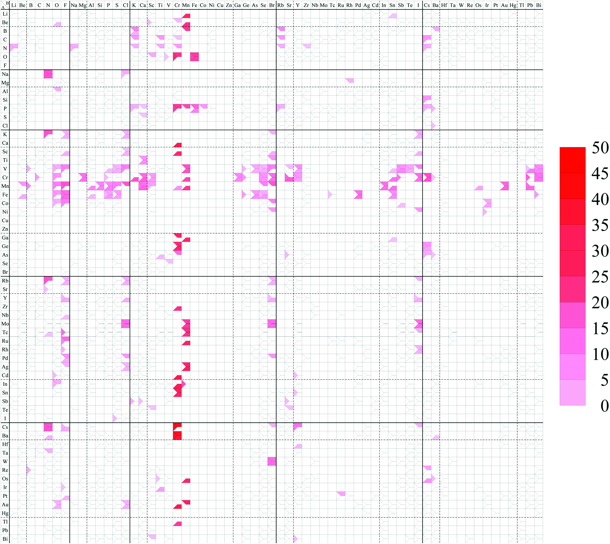 | ||
| Fig. 11 Spin magnetic moment map for AB2 type monolayers. The degree of intensity of red color represents the magnitude of the spin magnetic moment [μB per unit cell]. | ||
LiMn2, BeO2, BeSc2, BeCr2, BeMn2, BK2, BMn2, BRb2, BBa2, CK2, CTi2, CRb2, CCs2, NLi2, NNa2, NK2, NTi2, NCr2, NRb2, NCs2, OSc2, OCr2, OFe2, NaN2, NaCl2, MgRh2, AlO2, SiCs2, PK2, PCr2, PMn2, PFe2, PCo2, PRb2, PCs2, PBa2, SCa2, ClBa2, KN2, KF2, KCl2, KBr2, KI2, CaCr2, ScF2, ScCl2, ScCr2, ScBr2, ScI2, TiCa2, TiBr2, VB2, VO2, VF2, VP2, VS2, VCl2, VMn2, VGe2, VAs2, VSe2, VBr2, VSr2, VY2, VSn2, VSb2, VTe2, VI2, VPb2, VBi2, CrC2, CrO2, CrMg2, CrP2, CrK2, CrCa2, CrSc2, CrMn2, CrGa2, CrGe2, CrSe2, CrBr2, CrSr2, CrY2, CrSn2, CrSb2, CrI2, CrCs2, CrPb2, CrBi2, MnBe2, MnB2, MnO2, MnF2, MnAl2, MnSi2, MnP2, MnS2, MnCl2, MnCa2, MnSc2, MnCr2, MnMn2, MnSe2, MnBr2, MnIn2, MnSn2, MnOs2, MnAu2, MnPb2, FeBe2, FeO2, FeF2, FeAl2, FeP2, FeS2, FeGe2, FeAs2, FeSe2, FePd2, FeSn2, FeBi2, CoO2, CoF2, CoBr2, CoSb2, CoIr2, NiBr2, NiI2, NiIr2, GaCr2, GaMn2, GaSn2, GeCr2, GeCs2, AsTi2, AsCr2, AsSr2, AsCs2, AsBa2, RbN2, RbF2, RbCl2, RbBr2, RbI2, SrN2, YF2, YCl2, YBr2, YI2, ZrCr2, NbF2, MoCl2, MoMn2, MoBr2, MoI2, TcN2, TcF2, TcMn2, TcI2, RuF2, RuMn2, RhF2, RhI2, PdF2, PdCl2, PdBr2, AgF2, AgCl2, AgMn2, CdO2, CdCr2, CdY2, InO2, InCr2, InMn2, SnCr2, SnY2, SbK2, SbCa2, SbSr2, TeSc2, IS2, CsN2, CsF2, CsCr2, CsBr2, CsY2, CsI2, BaN2, BaCr2, HfY2, TaN2, WBr2, ReB2, ReCs2, OsMn2, OsCs2, OsBa2, IrTi2, PtF2, PtRu2, AuO2, AuCl2, AuCr2, AuMn2, TlCr2, BiSc2, BiY2.
D Comparison with ref. 67
A comparison with the database in ref. 67 for TMDCs and TMDOs is summarized in Table 10. In ref. 67, the authors carried out symmetry-constrained geometry optimizations for the prepared initial structures. Therefore, their symmetries were not changed during the geometry optimization. On the other hand, the unconstrained geometry optimizations we performed are a better way to obtain more stable structures since their structures can change from an unstable one to a stable one during the geometry optimizations, while the computational cost is much higher than that of the symmetry-constrained geometry optimization. In addition, the symmetry-unconstrained calculation has the possibility to obtain an unknown complicating structure which is totally different from the initial structure.
|
E Families of 1T/1H
The names of the specific compounds of the 1T/1H structures for each combination of groups in the periodic table are listed in the following subsections. For example, “I-XV (2)” means that atom A and atom B are in group I and XV, respectively. The total number of compounds in the family is written in the parentheses.E.1 Families of 1T
• I-I (2): RbK2, CsCs2.• I-XIII (1): LiAl2.
• I-XV (2): NaN2, KN2.
• II-I (2): BeRb2, BeCs2.
• II-II (2): BeCa2, BeBa2.
• II-TM (1): BeAu2.
• II-XIV (2): BeGe2, BePb2.
• II-XVI (1): BeTe2.
• II-XVII (16): MgF2, MgCl2, MgBr2, MgI2, CaF2, CaCl2, CaBr2, CaI2, SrF2, SrCl2, SrBr2, SrI2, BaF2, BaCl2, BaBr2, BaI2.
• TM-I (11): CrCs2, PdK2, PdRb2, PdCs2, AgCs2, PtK2, PtRb2, PtCs2, AuK2, AuRb2, AuCs2.
• TM-II (11): NiBe2, PdCa2, PdSr2, AgCa2, AgSr2, AgBa2, IrSr2, IrBa2, PtSr2, AuCa2, AuSr2.
• TM-TM (11): MnAu2, NiSc2, NiY2, RhY2, PdSc2, IrSc2, IrY2, IrZr2, PtSc2, PtY2, AuSc2.
• TM-XII (2): PtHg2, AuHg2.
• TM-XIII (9): PdTl2, AgAl2, IrIn2, IrTl2, PtGa2, PtIn2, PtTl2, AuAl2, AuIn2.
• TM-XV (4): TaN2, PtBi2, AuSb2, AuBi2.
• TM-XVI (39): ScTe2, TiS2, TiSe2, TiTe2, VS2, VSe2, CrO2, CrSe2, MnO2, MnS2, MnSe2, FeO2, FeS2, CoO2, NiO2, NiS2, NiSe2, ZrS2, ZrSe2, ZrTe2, NbS2, NbSe2, RhO2, PdO2, PdS2, PdSe2, PdTe2, HfS2, HfSe2, HfTe2, TaS2, TaSe2, IrO2, PtO2, PtS2, PtSe2, PtTe2, AuSe2, AuTe2.
• TM-XVII (27): ScBr2, ScI2, VF2, VCl2, VBr2, VI2, MnF2, MnCl2, MnBr2, FeF2, CoF2, CoBr2, NiBr2, NiI2, YF2, YBr2, YI2, TcI2, RuCl2, RuBr2, RhI2, PdF2, PdCl2, PdBr2, OsBr2, OsI2, IrI2.
• XII-I (1): HgCs2.
• XII-II (3): CdBa2, HgCa2, HgSr2.
• XII-XVII (5): CdF2, CdCl2, CdBr2, HgF2, HgCl2.
• XIII-I (2): BK2, BRb2.
• XIII-II (2): BMg2, BBa2.
• XIII-TM (11): BTi2, BNi2, BY2, BNb2, BPd2, BHf2, BTa2, BW2, BIr2, BPt2, InPd2.
• XIII-XIII (1): AlAl2
• XIII-XIV (3): BSi2, BGe2, BSn2.
• XIII-XVI (2): AlO2, InO2.
• XIII-XVII (1): TlI2.
• XIV-I (5): CK2, CRb2, CCs2, SiCs2, GeCs2.
• XIV-II (17): CBe2, CMg2, CCa2, CBa2, SiCa2, SiSr2, SiBa2, GeMg2, GeCa2, GeSr2, GeBa22, SnCa2, SnSr2, SnBa2, PbCa2, PbSr2, PbBa2.
• XIV-TM (10): CTi2, CV2, CCr2, CNi2, CY2, CNb2, CPd2, CAg2, CHf2, CTa2.
• XIV-XII (1): GeCd2.
• XIV-XIV (3): CGe2, CPb2, SiPb2.
• XIV-XVI (8): SiO2, SiS2, GeO2, GeSe2, GeTe2, SnO2, SnS2, PbO2.
• XIV-XVII (9): SiI2, GeCl2, GeBr2, SnBr2, SnI2, PbF2, PbCl2, PbBr2, PbI2.
• XV-I (10): NLi2, NNa2, NK2, NRb2, NCs2, PK2, PRb2, PCs2, AsCs2, SbK2.
• XV-II (10): NCa2, NSr2, PCa2, PSr2, PBa2, AsCa2, AsSr2, AsBa2, SbBa2, BiBa2.
• XV-TM (12): NTi2, NV2, NCr2, NNi2, NY2, NZr2, NNb2, NHf2, NTa2, PFe2, PY2, AsPd2.
• XV-XIII (2): PTl2, BiAl2.
• XV-XIV (4): NPb2, PSn2, PPb2, AsSn2.
• XV-XVI (11): PS2, PSe2, PTe2, AsS2, AsSe2, AsTe2, SbS2, SbSe2, SbTe2, BiS2, BiTe2.
• XVI-I (20): OLi2, ONa2, OK2, ORb2, OCs2, SLi2, SNa2, SK2, SRb2, SCs2, SeLi2, SeNa2, SeK2, SeRb2, SeCs2, TeLi2, TeNa2, TeK2, TeRb2, TeCs2.
• XVI-II (8): OMg2, SCa2, SSr2, SBa2, SeCa2, SeSr2, SeBa2, TeSr2.
• XVI-TM (9): OSc2, OTi2, OV2, OCr2, OFe2, ONb2, SSc2, SY2, SeY2.
• XVI-XIII (6): OIn2, OTl2, STl2, SeIn2, SeTl2, TeTl2.
• XVI-XIV (2): SSn2, SPb2.
• XVI-XVI (5): SeS2, SeSe2, TeS2, TeSe2, TeTe2.
• XVII-I (10): FNa2, FK2, FRb2, ClK2, ClRb2, ClCs2, BrK2, BrRb2, BrCs2, ICs2.
• XVII-II (7): ClCa2, ClSr2, ClBa2, BrCa2, BrSr2, BrBa2, ISr2.
• XVII-TM (1): ClY2.
• XVII-XII (1): FCd2.
• XVII-XIII (5): FIn2, FTl2, ClIn2, ClTl2, BrTl2.
E.2 Families of 1H
• I-TM (1): LiAg2.• I-XIII (1): LiAl2.
• I-XV (1): NaN2.
• I-XVII (5): KF2, KCl2, RbF2, RbCl2, RbBr2.
• II-II (3): BeBe2, BeCa2, BeBa2.
• II-TM (4): BeRh2, BePt2, BeAu2, SrAu2.
• II-XV (4): BeP2, BeSb2, BeBi2, BaN2.
• II-XVI (7): MgO2, CaO2, CaS2, CaSe2, CaTe2, SrSe2, BaS2.
• TM-TM (11): FePd2, NiSc2, RuPd2, PdSc2, PdAu2, HfAu2, OsZr2, PtSc2, PtY2, AuSc2, AuY2.
• TM-XII (1): ScHg2.
• TM-XIII (2): RhIn2, PdIn2.
• TM-XV (15): TiN2, VP2, VAs2, MnP2, ZrN2, ZrP2, NbP2, MoSb2, TcN2, TcSb2, TcBi2, HfP2, WAs2, ReN2, OsN2.
• TM-XVI (24): VS2, VSe2, VTe2, CrO2, CrS2, CrSe2, FeS2, FeSe2, NbO2, NbS2, NbSe2, NbTe2, MoO2, MoS2, MoSe2, MoTe2, TaO2, TaS2, TaSe2, TaTe2, WO2, WS2, WSe2, WTe2.
• TM-XVII (20): ScF2, ScCl2, ScBr2, ScI2, TiF2, TiCl2, TiBr2, FeF2, YF2, YCl2, YBr2, YI2, ZrF2, ZrCl2, ZrBr2, ZrI2, HfF2, HfCl2, HfBr2, HfI2.
• XII-II (5): CdCa2, CdBa2, HgCa2, HgSr2, HgBa2.
• XII-XV (1): CdBi2.
• XIII-TM (10): BNi2, BRu2, BRh2, BPd2, BW2, BRe2, BIr2, BPt2, AlPd2, AlPt2.
• XIII-XIII (2): InTl2, TlTl2.
• XIII-XV (1): AlSb2.
• XIV-TM (10): CCr2, CMo2, CRu2, CAg2, CW2, CRe2, SiPd2, SiPt2, GePd2, GePt2.
• XIV-XIV (8): CGe2, CPb2, SiGe2, SiSn2, SiPb2, GeGe2, GeSn2, SnPb2.
• XV-TM (4): NCr2, NNb2, NTa2, PFe2.
• XV-XIII (2): PTl2, BiAl2.
• XV-XIV (3): PGe2, PSn2, PPb2.
• XVI-II (5): SCa2, SeCa2, SeSr2, TeCa2, TeSr2.
• XVI-TM (9): OTi2, OV2, OCr2, OFe2, OZr2, ONb2, SSc2, SeSc2, SeY2.
• XVI-XIII (6): OIn2, OTl2, STl2, SeIn2, SeTl2, TeTl2.
• XVI-XIV (1): SSn2.
• XVII-I (7): FNa2, FK2, ClK2, ClRb2, BrK2, BrCs2, IK2.
• XVII-II (7): ClCa2, ClSr2, ClBa2, BrCa2, BrSr2, BrBa2, ISr2.
• XVII-TM (1): ClY2.
• XVII-XII (1): FCd2.
• XVII-XIII (3): FIn2, FTl2, ClIn2.
F NEB results for memory structures
NEB results for memory structures such as BeB, PdIr, CsAl, AuIr, HgPt, and PbBe are shown in Fig. 12. For each compound, five structures on the local minima are prepared to represent a model of a binary digit storage application. Each minimum energy path between two of them is obtained by optimizing 8 images on the path. The whole energy path is obtained by connecting all the minimum energy paths. The corresponding geometrical structures of images on the local energy minima are depicted in Fig. 12.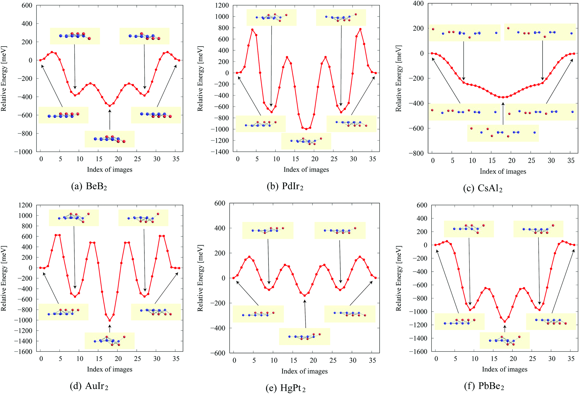 | ||
| Fig. 12 The NEB results for memory structures: (a) BeB2, (b) PdIr2, (c) CsAl2, (d) AuIr2, (e) HgPt2, and (f) PbBe2. | ||
Acknowledgements
M. F. and T. O. acknowledge the support of Priority Issue (creation of new functional devices and high-performance materials to support next-generation industries) to be tackled by using Post ‘K’ Computer, Ministry of Education, Culture, Sports, Science and Technology, Japan. J. Z. acknowledges the financial support of University of Science and Technology of China. The authors thank the Supercomputer Center, the Institute for Solid State Physics, the University of Tokyo for the use of the facilities.Notes and references
- P. Miró, M. Audiffred and T. Heine, Chem. Soc. Rev., 2014, 43, 6537 Search PubMed.
- B. Liu and K. Zhou, Prog. Mater. Sci., 2019, 100, 99 Search PubMed.
- Monatomic Two-Dimensional Layers: Modern Experimental Approaches for Structure, Properties, and Industrial Use, ed. M. Iwao, Elsevier, 2018 Search PubMed.
- Y. Feng, X. Wu, J. Hana and G. Gao, J. Mater. Chem. C, 2018, 6, 4087 Search PubMed.
- B. Liao, J. Zhou, B. Qiu, M. S. Dresselhaus and G. Chen, Phys. Rev. B: Condens. Matter Mater. Phys., 2015, 91, 235419 Search PubMed.
- M. Yoshida, T. Iizuka, Y. Saito, M. Onga, R. Suzuki, Y. Zhang, Y. Iwasa and S. Shimizu, Nano Lett., 2016, 16, 2061 Search PubMed.
- Q. H. Wang, K. Kalantar-Zadeh, A. Kis, J. N. Coleman and M. S. Strano, Nat. Nanotechnol., 2012, 7, 699 Search PubMed.
- K. F. Mak and J. Shan, Nat. Photonics, 2016, 10, 216 Search PubMed.
- N. Zibouche, A. Kuc, J. Musfeldt and T. Heine, Ann. Phys., 2014, 526, 395 Search PubMed.
- X. Li and X. Wu, Wiley Interdiscip. Rev.: Comput. Mol. Sci., 2016, 6, 441 Search PubMed.
- M. Ezawa, Phys. Rev. B: Condens. Matter Mater. Phys., 2013, 87, 155415 Search PubMed.
- H. Zeng, J. Dai, W. Yao, D. Xiao and X. Cui, Nat. Nanotechnol., 2012, 7, 490 Search PubMed.
- K. Chang and W. Chen, ACS Nano, 2011, 5, 4720 Search PubMed.
- E. Yoo, J. Kim, E. Hosono, H. S. Zhou, T. Kudo and I. Honma, Nano Lett., 2008, 8, 2277 Search PubMed.
- S. Das, D. Pandey, J. Thomas and T. Roy, Adv. Mater., 2019, 31, 1802722 Search PubMed.
- F. Schedin, A. K. Geim, S. V. Morozov, E. W. Hill, P. Blake, M. I. Katsnelson and K. S. Novoselov, Nat. Mater., 2007, 6, 652 Search PubMed.
- C. Ataca, E. Akturk, S. Ciraci and H. Ustunel, Appl. Phys. Lett., 2008, 93, 043123 Search PubMed.
- M. Zhou, Y. Lu, C. Zhang and Y. P. Feng, Appl. Phys. Lett., 2010, 97, 103109 Search PubMed.
- A. Damascelli, Z. Hussain and Z.-X. Shen, Rev. Mod. Phys., 2003, 75, 473 Search PubMed.
- C.-C. Lee, Y. Yamada-Takamura and T. Ozaki, J. Phys.: Condens. Matter, 2013, 25, 345501 Search PubMed.
- C.-C. Lee, M. Fukuda, Y.-T. Lee and T. Ozaki, J. Phys.: Condens. Matter, 2018, 30, 295502 Search PubMed.
- C. S. Fadley and D. A. Shirley, Phys. Rev. Lett., 1968, 21, 980 Search PubMed.
- T. Ozaki and C.-C. Lee, Phys. Rev. Lett., 2017, 118, 026401 Search PubMed.
- G. Binnig, H. Rohrer, Ch Gerber and E. Weibel, Appl. Phys. Lett., 1982, 40, 178 Search PubMed.
- J. Tersoff and D. R. Hamann, Phys. Rev. B: Condens. Matter Mater. Phys., 1985, 31, 805 Search PubMed.
- L. Feng, K. Yabuoshi, Y. Sugimoto, J. Onoda, M. Fukuda and T. Ozaki, Phys. Rev. B, 2018, 98, 195311 Search PubMed.
- A. K. Geim and K. S. Novoselov, Nat. Mater., 2007, 6, 183 Search PubMed.
- K. Takeda and K. Shiraishi, Phys. Rev. B: Condens. Matter Mater. Phys., 1994, 50, 14916 Search PubMed.
- B. Aufray, A. Kara, S. Vizzini, H. Oughaddou, C. Leandri, B. Ealet and G. Le, Appl. Phys. Lett., 2010, 96, 183102 Search PubMed.
- B. Lalmi, H. Oughaddou, H. Enriquez, A. Karae, S. Vizzini, B. Ealet and B. Aufray, Appl. Phys. Lett., 2010, 97, 223109 Search PubMed.
- A. Fleurence, R. Friedlein, T. Ozaki, H. Kawai, Y. Wang and Y. Yamada-Takamura, Phys. Rev. Lett., 2012, 108, 245501 Search PubMed.
- C.-C. Lee, A. Fleurence, Y. Yamada-Takamura, T. Ozaki and R. Friedlein, Phys. Rev. B: Condens. Matter Mater. Phys., 2014, 90, 075422 Search PubMed.
- C.-C. Lee, J. Yoshinobu, K. Mukai, S. Yoshimoto, H. Ueda, R. Friedlein, A. Fleurence, Y. Yamada-Takamura and T. Ozaki, Phys. Rev. B, 2017, 95, 115437 Search PubMed.
- E. Bianco, S. Butler, S. Jiang, O. D. Restrepo, W. Windl and J. E. Goldberger, ACS Nano, 2013, 7, 4414 Search PubMed.
- M. E. Dávila, L. Xian, S. Cahangirov, A. Rubio and G. L. Lay, New J. Phys., 2014, 16, 095002 Search PubMed.
- Y. Shao, Z.-L. Liu, C. Cheng, X. Wu, H. Liu, C. Liu, J.-O. Wang, S.-Y. Zhu, Y.-Q. Wang, D.-X. Shi, K. Ibrahim, J.-T. Sun, Y.-L. Wang and H.-J. Gao, Nano Lett., 2018, 18, 2133 Search PubMed.
- A. J. Mannix, X.-F. Zhou, B. Kiraly, J. D. Wood, D. Alducin, B. D. Myers, X. Liu, B. L. Fisher, U. Santiago, J. R. Guest, M. J. Yacaman, A. Ponce, A. R. Oganov, M. C. Hersam and N. P. Guisinger, Science, 2015, 350, 1513 Search PubMed.
- B. Feng, J. Zhang, Q. Zhong, W. Li, S. Li, H. Li, P. Cheng, S. Meng, L. Chen and K. Wu, Nat. Chem., 2016, 8, 563 Search PubMed.
- F.-F. Zhu, W.-J. Chen, Y. Xu, C.-L. Gao, D.-D. Guan, C.-H. Liu, D. Qian, S.-C. Zhang and J.-F. Jia, Nat. Mater., 2015, 14, 1020 Search PubMed.
- H. Liu, Y. Du, Y. Denga and P. D. Ye, Chem. Soc. Rev., 2015, 44, 2732 Search PubMed.
- F. Reis, G. Li, L. Dudy, M. Bauernfeind, S. Glass, W. Hanke, R. Thomale, J. Schafer and R. Claessen, Science, 2017, 357, 287 Search PubMed.
- Y. Lin, T. V. Williams and J. W. Connell, J. Phys. Chem. Lett., 2010, 1, 277 Search PubMed.
- T. Takahashi, S. Nakatani, N. Okamoto, T. Ishikawa and S. Kikuta, Jpn. J. Appl. Phys., 1988, 27, L753 Search PubMed.
- H. Aizawa, M. Tsukada, N. Sato and S. Hasegawa, Surf. Sci., 1999, 429, L509 Search PubMed.
- B. Feng, B. Fu, S. Kasamatsu, S. Ito, P. Cheng, C.-C. Liu, Y. Feng, S. Wu, S. K. Mahatha, P. Sheverdyaeva, P. Moras, M. Arita, O. Sugino, T.-C. Chiang, K. Shimada, K. Miyamoto, T. Okuda, K. Wu, L. Chen, Y. Yao and I. Matsuda, Nat. Commun., 2017, 8, 1007 Search PubMed.
- L.-M. Yang, V. Baičić, I. A. Popov, A. I. Boldyrev, T. Heine, T. Frauenheim and E. Ganz, J. Am. Chem. Soc., 2015, 137, 2757 Search PubMed.
- M. Hashimoto, Y. Fukaya, A. Kawasuso and A. Ichimiya, e-J. Surf. Sci. Nanotechnol., 2009, 7, 436 Search PubMed.
- J. Zhou, J. Lin, X. Huang, Y. Zhou, Y. Chen, J. Xia, H. Wang, Y. Xie, H. Yu, J. Lei, D. Wu, F. Liu, Q. Fu, Q. Zeng, C.-H. Hsu, C. Yang, L. Lu, T. Yu, Z. Shen, H. Lin, B. I. Yakobson, Q. Liu, K. Suenaga, G. Liu and Z. Liu, Nature, 2018, 556, 355 Search PubMed.
- K. Takada, H. Sakurai, E. Takayama-Muromachi, F. Izumi, R. A. Dilanian and T. Sasaki, Nature, 2003, 422, 53 Search PubMed.
- Y. Omomo, T. Sasaki and M. Watanabe, J. Am. Chem. Soc., 2003, 125, 3568 Search PubMed.
- M. Shikano, C. Delmas and J. Darriet, Inorg. Chem., 2004, 43, 1214 Search PubMed.
- M. Naguib, V. N. Mochalin, M. W. Barsoum and Y. Gogotsi, Adv. Mater., 2014, 26, 992 Search PubMed.
- H. Tanga, Q. Hua, M. Zhenga, Y. Chia, X. Qina, H. Panga and Q. Xu, Prog. Nat. Sci.: Mater. Int., 2018, 28, 133 Search PubMed.
- J. Zhu, E. Ha, G. Zhao, Y. Zhou, D. Huang, G. Yue, L. Hub, N. Sun, Y. Wang, L. Y. S. Lee, C. Xu, K.-Y. Wong, D. Astruc and P. Zhao, Coord. Chem. Rev., 2017, 352, 306 Search PubMed.
- S. V. Badalov, M. Yagmurcukardes, F. M. Peeters and H. Sahin, J. Phys. Chem. C, 2018, 122, 28302 Search PubMed.
- V. Sreepal, M. Yagmurcukardes, K. S. Vasu, D. J. Kelly, S. F. R. Taylor, V. G. Kravets, Z. Kudrynskyi, Z. D. Kovalyuk, A. Patanè, A. N. Grigorenko, S. J. Haigh, C. Hardacre, L. Eaves, H. Sahin, A. K. Geim, F. M. Peeters and R. R. Nair, Nano Lett., 2019, 19, 6475 Search PubMed.
- M. Yagmurcukardes, Phys. Rev. B, 2019, 100, 024108 Search PubMed.
- A.-Y. Lu, H. Zhu, J. Xiao, C.-P. Chuu, Y. Han, M.-H. Chiu, C.-C. Cheng, C.-W. Yang, K.-H. Wei, Y. Yang, Y. Wang, D. Sokaras, D. Nordlund, P. Yang, D. A. Muller, M.-Y. Chou, X. Zhang and L.-J. Li, Nat. Nanotechnol., 2017, 12, 744 Search PubMed.
- M. Yagmurcukardes and F. M. Peeters, Phys. Rev. B, 2020, 101, 155205 Search PubMed.
- A. Zunger, Phys. Rev. B: Condens. Matter Mater. Phys., 1980, 22, 5839 Search PubMed.
- P. Villars, J. Less-Common Met., 1983, 92, 215 Search PubMed.
- D. G. Pettifor, Solid State Commun., 1984, 51, 31 Search PubMed.
- D. G. Pettifor, Mater. Sci. Technol., 1988, 8, 675 Search PubMed.
- C. Ataca, H. Sahin and S. Ciraci, J. Phys. Chem. C, 2012, 116, 8983 Search PubMed.
- X. Zhang, Z. Lai, Q. Ma and H. Zhang, Chem. Soc. Rev., 2018, 47, 3301 Search PubMed.
- F. A. Rasmussen and K. S. Thygesen, J. Phys. Chem. C, 2015, 119, 13169 Search PubMed.
- S. Haastrup, M. Strange, M. Pandey, T. Deilmann, P. S. Schmidt, N. F. Hinsche, M. N. Gjerding, D. Torelli, P. M. Larsen, A. C. Riis-Jensen, J. Gath, K. W. Jacobsen, J. J. Mortensen, T. Olsen and K. S. Thygesen, 2D Mater., 2018, 5, 042002 Search PubMed.
- M. Ashton, J. Paul, S. B. Sinnott and R. G. Hennig, Phys. Rev. Lett., 2017, 118, 106101 Search PubMed.
- W. Kohn and L. J. Sham, Phys. Rev., 1965, 140, A1133 Search PubMed.
- J. P. Perdew, K. Burke and M. Ernzerhof, Phys. Rev. Lett., 1996, 77, 3865 Search PubMed.
- T. Ozaki, et al., OpenMX package, http://www.openmx-square.org/ Search PubMed.
- I. Morrison, D. M. Bylander and L. Kleinman, Phys. Rev. B: Condens. Matter Mater. Phys., 1993, 47, 6728 Search PubMed.
- T. Ozaki, Phys. Rev. B: Condens. Matter Mater. Phys., 2003, 67, 155108 Search PubMed.
- K. Lejaeghere, et al. , Science, 2016, 351, aad3000 Search PubMed.
- T. Ozaki and H. Kino, Phys. Rev. B: Condens. Matter Mater. Phys., 2005, 72, 045121 Search PubMed.
- A. Banerjee, N. Adams, J. Simons and R. Shepard, J. Phys. Chem., 1985, 89, 52 Search PubMed.
- P. Csaszar and P. Pulay, THEOCHEM, 1984, 114, 31 Search PubMed.
- (a) C. G. Broyden, J. Inst. Math. Its Appl., 1970, 6, 76 Search PubMed; (b) R. Fletcher, Comput. J., 1970, 13, 317 Search PubMed; (c) D. Goldrarb, Math. Comp., 1970, 24, 23 Search PubMed; (d) D. F. Shanno, Math. Comp., 1970, 24, 647 Search PubMed.
- A. Kuc and T. Heine, Chem. Soc. Rev., 2015, 44, 2603 Search PubMed.
- E. Clementi, D. L. Raimondi and W. P. Reinhardt, J. Chem. Phys., 1967, 47, 1300 Search PubMed.
- Mathematica, Version 11.2, Wolfram Research, Inc., Champaign, IL, 2017 Search PubMed.
- B. Eifert and C. Heiliger, Crystallica: A package to plot crystal structures (library.wolfram.com/infocenter/MathSource/9372/).
- A. Togo and I. Tanaka, arXiv:1808.01590 [cond-mat.mtrl-sci], Spglib package (github.com/atztogo/spglib/).
- In the program code Spglib, the distance tolerance is defined as tolerance of distance between atomic positions and between lengths of lattice vectors to be tolerated in the symmetry finding. Since the optimized structures are calculated by using a 2 × 2 supercell, the distance between the center of symmetry and the farthest atom from it is more than about 10 Å. Therefore, the tolerance 0.5 Å for our system means tolerance of about 5% of distance between atomic positions. In other words, an atom may be as far as “5% of distance from the center of symmetry” away from the position where it ought to be according to symmetry. For example, the 5% tolerance means that the gap of the distance from the nearest neighboring atom (∼1 Å) is about 0.05 Å, which is small enough to compare with experimental STM images.
- Our structure map and database are available on the interactive website, http://www.openmx-square.org/2d-ab2/.
- Y.-T. Lee and T. Ozaki, J. Mol. Graphics Modell., 2019, 89, 192 Search PubMed , OpenMX Viewer is available in http://www.openmx-square.org/viewer/.
- Q.-Y. Wang, Z. Li, W.-H. Zhang, Z.-C. Zhang, J.-S. Zhang, W. Li, H. Ding, Y.-B. Ou, P. Deng, K. Chang, J. Wen, C.-L. Song, K. He, J.-F. Jia, S.-H. Ji, Y.-Y. Wang, L.-L. Wang, X. Chen, X.-C. Ma and Q.-K. Xue, Chin. Phys. Lett., 2012, 29, 037402 Search PubMed.
- K. Sugawara, Y. Nakata, R. Shimizu, P. Han, T. Hitosugi, T. Sato and T. Takahashi, ACS Nano, 2016, 10, 1341 Search PubMed.
- P. Chen, W. W. Pai, Y.-H. Chan, A. Takayama, C.-Z. Xu, A. Karn, S. Hasegawa, M. Y. Chou, S.-K. Mo, A.-V. Fedorov and T.-C. Chiang, Nat. Commun., 2017, 8, 516 Search PubMed.
- S. Mañas-Valero, V. García-López, A. Cantarero and M. Galbiati, Appl. Sci., 2016, 6, 264 Search PubMed.
- P. Tsipas, D. Tsoutsou, S. Fragkos, R. Sant, C. Alvarez, H. Okuno, G. Renaud, R. Alcotte, T. Baron and A. Dimoulas, ACS Nano, 2018, 122, 1696 Search PubMed.
- K. Xu, Z. Wang, F. Wang, Y. Huang, F. Wang, L. Yin, C. Jiang and J. He, Adv. Mater., 2015, 27, 7881 Search PubMed.
- R. Yue, A. T. Barton, H. Zhu, A. Azcatl, L. F. Pena, J. Wang, X. Peng, N. Lu, L. Cheng, R. Addou, S. McDonnell, L. Colombo, J. W. P. Hsu, J. Kim, M. J. Kim, R. M. Wallace and C. L. Hinkle, ACS Nano, 2015, 91, 474 Search PubMed.
- H. Ryu, Y. Chen, H. Kim, H.-Z. Tsai, S. Tang, J. Jiang, F. Liou, S. Kahn, C. Jia, A. A. Omrani, J. H. Shim, Z. Hussain, Z.-X. Shen, K. Kim, B. I. Min, C. Hwang, M. F. Crommie and S.-K. Mo, Nano Lett., 2018, 18, 689 Search PubMed.
- Y. Zhao, J. Qiao, P. Yu, Z. Hu, Z. Lin, S. P. Lau, Z. Liu, W. Ji and Y. Chai, Adv. Mater., 2016, 28, 2399 Search PubMed.
- J. A. Wilson and A. D. Yoffe, Adv. Phys., 1969, 18, 193 Search PubMed.
- M. A. McGuire, Crystals, 2017, 7, 121 Search PubMed.
- V. V. Kulish and W. Huang, J. Mater. Chem. C, 2017, 5, 8734 Search PubMed.
- N. D. Mermin and H. Wagner, Phys. Rev. Lett., 1966, 17, 1133 Search PubMed.
- B. Huang, G. Clark, E. Navarro-Moratalla, D. R. Klein, R. Cheng, K. L. Seyler, D. Zhong, E. Schmidgall, M. A. McGuire, D. H. Cobden, W. Yao, D. Xiao, P. Jarillo-Herrero and X. Xu, Nature, 2017, 546, 270 Search PubMed.
- S. H. Lin and J. L. Kuo, Phys. Chem. Chem. Phys., 2014, 16, 20763 Search PubMed.
- K. J. Donald and R. Hoffmann, J. Am. Chem. Soc., 2006, 128, 11236 Search PubMed.
- K. J. Donald, M. Hargittai and R. Hoffmann, Chem. – Eur. J., 2009, 15, 158 Search PubMed.
- W. Sun, Y. Li, B. Wang, X. Jiang, M. I. Katsnelson, P. Korzhavyi, O. Erikssona and I. Di Marco, Nanoscale, 2016, 8, 15753 Search PubMed.
- M. Wu, B. Wang, Q. Hu, L. Wang and A. Zhou, Materials, 2018, 11, 2112 Search PubMed.
- X. Zhang, Z. Xiao, H. Lei, Y. Toda, S. Matsuishi, T. Kamiya, S. Ueda and H. Hosono, Chem. Mater., 2014, 26, 6638 Search PubMed.
- K. Lee, S. W. Kim, Y. Toda, S. Matsuishi and H. Hosono, Nature, 2013, 494, 336 Search PubMed.
- G. Ying, A. D. Dillon, A. T. Fafarman and M. W. Barsoum, Mater. Res. Lett., 2017, 5, 391 Search PubMed.
- W. S. Zhi, K. D. Fredrickson, B. Anasori, J. Kibsgaard, A. L. Strickler, M. R. Lukatskaya, Y. Gogotsi, T. F. Jaramillo and A. Vojvodic, ACS Energy Lett., 2016, 1, 589 Search PubMed.
- M. Naguib, J. Halim, J. Lu, K. M. Cook, L. Hultman, Y. Gogotsi and M. W. Barsoum, J. Am. Chem. Soc., 2013, 135, 15966 Search PubMed.
- C. Chen, X. Ji, K. Xu, B. Zhang, L. Miao and J. Jiang, ChemPhysChem, 2017, 18, 1897 Search PubMed.
- S. Wang, H. Ge, S. Sun, J. Zhang, F. Liu, X. Wen, X. Yu, L. Wang, Y. Zhang, H. Xu, J. C. Neuefeind, Z. Qin, C. Chen, C. Jin, Y. Li, D. He and Y. Zhao, J. Am. Chem. Soc., 2015, 137, 4815 Search PubMed.
- F. Kawamura, H. Yusa and T. Taniguchi, Appl. Phys. Lett., 2012, 100, 251910 Search PubMed.
- A. F. Young, C. Sanloup, E. Gregoryanz, S. Scandolo, R. J. Hemley and H.-K. Mao, Phys. Rev. Lett., 2006, 96, 155501 Search PubMed.
- J. C. Crowhurst, A. F. Goncharov, B. Sadigh, C. L. Evans, P. G. Morrall, J. L. Ferreira and A. J. Nelson, Science, 2006, 311, 1275 Search PubMed.
- Y. Wang and Y. Ding, J. Phys. Chem. C, 2018, 122, 26748 Search PubMed.
- C. Hua, F. Sheng, Q. Hu, Z.-A. Xu, Y. Lu and Y. Zheng, J. Phys. Chem. Lett., 2018, 9, 6695 Search PubMed.
- K. Gao, IEEE Magn. Lett., 2018, 9, 1–5 Search PubMed.
- Ultra-High-Density Magnetic Recording: Storage Materials and Media Designs, ed. G. Varvaro and F. Casoli, Jenny Stanford Publishing, 2016 Search PubMed.
- G. Henkelman and H. Jonsson, J. Chem. Phys., 2000, 113, 9978 Search PubMed.
- Y. Shao, M. Shao, Y. Kawazoe, X. Shi and H. Pan, J. Mater. Chem. A, 2018, 6, 10226 Search PubMed.
Footnote |
| † Electronic supplementary information (ESI) available. See DOI: 10.1039/d0ma00999g |
| This journal is © The Royal Society of Chemistry 2021 |