
 Open Access Article
 This Open Access Article is licensed under a Creative Commons Attribution-Non Commercial 3.0 Unported Licence
Oxidized eutectic gallium–indium (EGaIn) nanoparticles for broadband light response in a graphene-based photodetector†
Pengfei
Wang
a,
Qianqian
Hu
b,
Bocheng
Lv
b,
Yu
Liu
a,
Jun
Yin
c and
Jialin
Sun
 *b
*b
aCollege of Mechanical Engineering and Automation, Fuzhou University, Fuzhou 350108, P. R. China
bDepartment of Physics, State Key Laboratory of Low-Dimensional Quantum Physics, Tsinghua University, Beijing 100084, P. R. China. E-mail: jlsun@mail.tsinghua.edu.cn
cSchool of Materials Science and Engineering, National Institute for Advanced Materials, Nankai University, Tianjin 300350, P. R. China
First published on 25th May 2021
Abstract
Graphene is considered to be a valuable material in the field of photodetection due to its ultra-high electron mobility. However, its weak light absorption, short carrier lifetime and lack of gain mechanism limit the light responsivity of graphene at the magnitude of mA W−1. Herein, based on the oxidation characteristics of eutectic gallium–indium (EGaIn) alloy and the adoption of low-cost physical vapor deposition methods, we develop nanoparticles with gradient changes in elements to solve the drawback of common quantum dots of a narrow response band, fabricating a composite nanostructure of suspended graphene and oxidized EGaIn nanoparticles. The photodetector achieves wide-spectrum and high-performance detection from ultraviolet to near-infrared, with a responsivity enhancement of three order magnitude compared to that of pristine graphene. Then, the enhancement mechanism is analysed through structural characterization and control experiments, proving the dominant effect of oxidized nanoparticles on improving the responsivity and response band. This paper expands the application of EGaIn in the field of photoelectric detection and offers new idea for constructing high-performance quantun-dot based photodetectors.
1. Introduction
Photodetectors have long been a focus of research due to their widespread applications, including imaging, communication, sensing, meteorological and environment observations.1–5 With the continuous development of Moore's law, the demand for miniaturized and high-performance photodetectors is becoming increasingly urgent. The emerging two-dimensional materials from 2004 can meet this development demand due to their properties such as small size, controllable performance and easy integration.6 Among them, graphene has become the preferred material to develop a new generation of photodetectors due to its ultra-high electron–hole mobility,7,8 rich and diverse physical mechanisms,9,10 and more mature preparation and transfer methods.11–14 However, graphene still has some undesirable properties, such as its limited optical absorption and short lifetime of photo-generated carriers;15–17 therefore, it cannot fully meet the requirements of high-performance photodetectors. In recent years, a variety of methods to increase the light absorption of graphene have been developed, such as plasmon of noble metals18,19 or resonance of microcavities;20,21 however, the results are not obvious. The commonly adopted way is to composite different kinds of semiconductor materials on graphene, and the formed junction on the contact interface can greatly improve the absorption and carrier transport. Among them, the composite structure based on zero-dimensional quantum dots (QDs) has received extensive attention due to its low cost, simple preparation, and high efficiency.22–24 However, owing to the discrete energy structure of quantum dots, its light absorption band is narrow, which has limits for broadband detection. There has been research to improve the response of quantum-dot-based devices.25–27 However, the responsivity, response speed and response band performance generally cannot be optimized at the same time, and the complex structure design also increases the difficulty of the fabrication and application; therefore, much effort is still needed.The energy band structure is an inherent property of a material, and it generally depends on the chemical composition and crystal structure of the material. In recent years, there has been research work on adjusting the energy band by adjusting the chemical composition of alloy materials, such as ternary alloys of InP and InAs, ternary alloys of ZnS and ZnSe, and alloys of group III nitrides, which has shown good development in the photoelectric field.28–30 Although the energy gap of the alloy material can be adjusted, the band gap is also fixed after preparation due to the fixed material composition. Further, researchers have developed spatial bandgap engineering and successfully prepared CdSxSe1−x nanowire structures with gradient changes in chemical composition along the axis of nanowires, and the photoelectric performance has been significantly improved.31–33
For quantum dots, size changes and composition changes can adjust the energy band gap.34 In terms of size, the integration of quantum dots with different sizes or different kinds of quantum dots to achieve broad spectrum absorption is helpful and useful; however, there are many limitations in their preparation and application, such as aggregation of quantum dots and limited energy-band changes. Inspired by work about composition changes of nanowires, realizing the gradient change of a chemical composition on a single quantum dot will greatly improve the optoelectronic properties of quantum dots. However, because all three dimensions of quantum dots are on the nanometer scale, it is a challenging task to artificially synthesize quantum dots with gradient changes in chemical composition. It would be a valuable breakthrough to synthesize nanoparticles or quantum dots with the above characteristics by using natural oxidation processes.
Eutectic gallium–indium (EGaIn) alloy is an emerging liquid metal material that has received widespread attention in recent years and has been used in flexible circuits, electronic skin and sensors.35,36 Under ambient conditions, the surface of the alloy will be oxidized into the semiconductor37 gallium oxide (Ga2O3) with a band gap of 4.8 eV, which is a material commonly used for ultraviolet detection.38 Additionally, due to the barrier of the surface oxide layer, the internal oxidation will decrease. Thus, EGaIn nanostructures with a gradient of chemical composition from outside to inside can be naturally formed. Our previous work39 based on EGaIn nanofilm confirmed its wide-band absorption capacity. The existing results40 show that a small size is more conducive to the formation of oxide film and enhances its effects. For this reason, it is necessary to investigate EGaIn nanoparticles and their photoelectric enhancement of two-dimensional materials.
Here, uniformly distributed EGaIn nanoparticles (NPs) are prepared on PMMA-assisted suspended graphene by an evaporation method and a graphene-based composite photodetector is fabricated. The naturally oxidizable property of EGaIn is utilized. The process of oxidation causes the oxygen content of the nanoparticles to be distributed in a gradient from the outside to the inside, causing the material composition of the particles to gradually change from the outer large-bandgap semiconductor Ga2O3 to the inner metal EGaIn. Benefiting from the broadband light absorption of oxidized EGaIn nanoparticles and the ultra-high mobility of suspended graphene, the photodetector achieves a high responsivity of about 5 A W−1 from ultraviolet to near-infrared light. On the one hand, this research has described the preparation of new high-performance photodetectors; on the other hand, it has improved the shortcomings of quantum dot-based photodetectors in the detection band and provided new ideas for the further development of photoelectric devices.
2. Experimental
2.1 Preparation of EGaIn nanoparticles
Metal gallium and indium (99.999%, Shanghai Macklin Biochemical Co., Ltd, China) with quantitative proportioning are physically processed by heating, melting and natural cooling to prepare the liquid EGaIn alloy. The vacuum thermal evaporation method is adopted to realize the preparation of EGaIn nanoparticles on the substrate. The amount of evaporated mass decides the diameter and density of the fabricated nanoparticles. In the experiment, liquid EGaIn with a mass of 50 mg is deposited on the graphene under a vacuum of 3 × 10⁻³ Pa.2.2 Preparation of the photodetector prototype device
The substrate is processed by depositing a 100 nm nitride layer as an isolating layer on the silicon wafer. The narrow slit in the substrate is etched using lithography and shaped into a 1.5 mm-long, 100 μm-wide rectangular slit. The 35 nm-thick gold films are evaporated on the sides of the slit as electrodes. The CVD-grown few-layer graphene was purchased from XF NANO-Advanced Materials Supplier. The PMMA is spin-cast on the graphene to realize the transfer of graphene onto the Si/Si3N4 substrate. The rectangular slit on the substrate results in a section of suspended PMMA-assisted graphene. Then, liquid EGaIn with a mass of 50 mg is deposited on the suspended graphene under a vacuum of 3 × 10⁻³ Pa. The oxidization of the nanoparticles is realized by placing them in an oxygen environment for 30 days.2.3 Structural characteristics and testing of optoelectronic properties
The morphology of the EGaIn nanoparticles was characterized by scanning electron microscopy (SEM) (S-5500, Hitachi). Auger electron spectroscopy (AES) (PHI-700, ULVAC-PHI) was used to characterize the element distribution in depth. The high voltage of the Ar+ electron gun was 3 kV, and the energy resolution was 1%. The incident angle was 30°, and the vacuum of the analysis chamber was lower than 3.9 × 10⁻⁹ Torr. The light source was provided by lasers with wavelengths of 375 nm, 405 nm, 523 nm, 635 nm and 808 nm, possessing spot diameters of 3.6 mm, 2.8 mm, 1.9 mm, 3.8 mm and 4.4 mm, respectively. Current–voltage (I–V) curves and photoelectric responses of the fabricated device were measured by a Source-Meter (Keithley 2400). Optical micrograph, Raman spectrum and micro-area photoelectric response analyses were carried out with a multifunctional and high resolution near-field optoelectronic and spectroscopic imaging microscope (Alpha 300RAS, WITec).3. Results and discussion
Suspended PMMA-assisted graphene was realized by transferring it onto a Si/Si3N4 substrate with a 1.5 mm-long and 100 μm-wide rectangular slit, as shown in Fig. 1a. The dark area is the suspended part, while the bright area is the supported part. The uneven color on the film originates from many causes, such as the insulating substrate and PMMA, which would have no obvious effect on the following photo-electric measurements. Then, the EGaIn nanoparticles were evaporated onto the graphene through the slit, as shown in Fig. 1b. The topography of the nanoparticles deposited on suspended graphene can be seen in Fig. 1c. The EGaIn nanoparticles are relatively evenly distributed on the graphene, and each particle has a good morphology, is approximately spherical in structure, and is independent of the other particles. The sizes of the nanoparticles are not uniform, and the diameter is distributed between several nanometers and tens of nanometers. The aggregation effect of wet-synthesized nanoparticles was avoided by adopting the low-cost evaporation method, which facilitates research based on the multi-size integration effect of nanoparticles. The inset is a cross-section SEM image of the prepared sample, showing that the nanoparticles are hemispherical in structure on the graphene; this results from the formation of an oxide layer on the surface of the nanoparticles, which reduces the surface tension and forms better wettability with the graphene surface.41 The topography is the same with the EGaIn nanoparticles on the supported graphene, as shown in Fig. S1 (ESI†), indicating that the suspension would not have an obvious effect on the morphology of the nanoparticles. The red, blue and pink squares (5 μm × 5 μm) shown in Fig. 1a and b are measuring locations for Raman spectra, corresponding to supported graphene, suspended graphene and suspended graphene composited with EGaIn nanoparticles, respectively. The Raman spectra are shown in Fig. 1d in the same colors as the corresponding squares. For the red spectral line in Fig. 1d, the characteristic peaks of graphene at ∼1590 cm−1 and ∼2685 cm−1 are clearly seen, and the peak at ∼1350 cm−1 is associated with graphene edges and sub-domain boundaries.42 The peak at 520 cm−1 comes from silicon, and the peaks at 950–1000 cm−1 are due to the isolating layers of Si3N4 formed at different temperatures.43 For the Raman spectrum of suspended graphene in the blue spectral line, the peaks have a small red shift; this can be seen more clearly in the magnified plot of the Raman peaks shown in Fig. S2 (ESI†), due to the absence of graphene–substrate interactions.44 When compositing with oxidized EGaIn nanoparticles, the Raman spectrum (see the green spectral line) adds an envelope on the background, the peak position is red-shifted, and the peak width has an increase, which comes from the interaction between graphene and nanoparticles. A schematic of the device structure is shown in Fig. 1e, and the laser can illuminate the composite part through the slit from the bottom.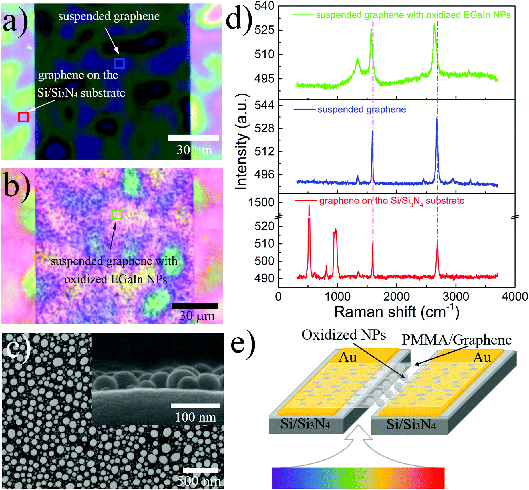 | ||
| Fig. 1 Characterization of oxidized EGaIn nanoparticles on suspended graphene. (a) Microscope images of few-layer graphene suspended on Si/Si3N4 substrate with a 100 μm-wide slit. (b) Microscope image of suspended graphene composited with oxidized EGaIn nanoparticles. The 5 μm × 5 μm squares in the (a) and (b) are the measuring location for the Raman spectra. (c) The SEM image of oxidized EGaIn nanoparticles on the suspended graphene. The inset shows cross-section SEM images of EGaIn on the graphene. (d) The Raman spectra for graphene on the Si/Si3N4 substrate, suspended graphene and suspended graphene with oxidized EGaIn nanoparticles. (e) Schematic of the device structure. The laser can illuminate the composite part through the slit from the bottom. | ||
Then, the oxidation of EGaIn nanoparticles was explored. Because the EGaIn nanoparticles on suspended graphene cannot be used for related characterization experiments, we used composite samples of graphene and EGaIn prepared on the substrate, as shown in Fig. S1 (ESI†). From the above research, we already know that the presence or absence of substrate has no significant effect on the morphology of the indium gallium alloy. The AES characterization in Fig. 2a exhibits the element distribution of the nanoparticles from the outside to the inside. Only gallium and oxygen are present on the surface of the particles, and indium is distributed in the inner layer. With the layer-by-layer sputter of the nanoparticles by high-energy ions, we found that the content of indium and gallium remained basically unchanged, while the oxygen content gradually decreased with the depth. There is only a small amount of oxygen at a depth of 9 nm inside. The detailed change of the elemental content can be seen in Fig. S3 (ESI†). Compared with the bulk material, the EGaIn nanoparticles produced by our method can reach 9 nm in the thickness of the oxide layer; this originates from the newly adopted method, which produces smaller nanoparticles and facilitates the deep oxidization of absorbed oxygen on the surface. The Raman spectrum shown in Fig. 2b obviously exhibits the characteristic peaks of Ga2O3, indicating that oxidation does exist on the nanoparticle and has a relatively large proportion in the whole nanoparticle. Therefore, it can be determined that the particles form a gradient distribution of oxygen from the outside to the inside, the outer layer is dominated by Ga2O3, and the innermost layer is still metal EGaIn. Indium is more difficult to oxidize than gallium,45 and a segregated metal indium layer is formed underneath the oxide layer. The oxide layer with a thickness of approximately 10 nm occupies a considerably large proportion in the whole nanoparticle, whose diameter is only a few nanometers or tens of nanometers.
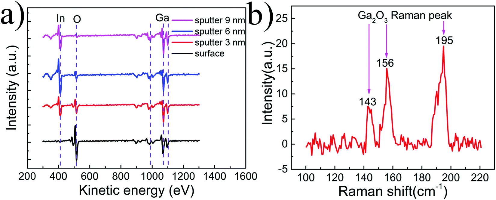 | ||
| Fig. 2 Characterization of oxidized EGaIn nanoparticles. (a) AES spectrum of EGaIn nanoparticles at the surface and the depths of 3 nm, 6 nm and 9 nm. The nanoparticles are sputtered by high-energy ions. (b) Raman spectrum of EGaIn to reveal the oxidation of the nanoparticles. | ||
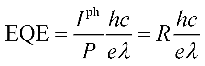
Next, a photodetector prototype device based on the composites of suspended graphene and EGaIn nanoparticles was fabricated and the photoelectric responses were measured. The detailed manufacturing process can be seen in Fig. S4 (ESI†). Graphene acts as the only carrier transport channel, and its contact with the gold electrode shows the linear current–voltage relationship and indicates ohmic contact with the electrodes (Fig. 3a). The lasers with wavelengths of 375 nm, 405 nm, 532 nm, 635 nm and 808 nm illuminated the composite part of suspended graphene and oxidized EGaIn through the slit, and the photoelectric responses were measured, as shown in Fig. 3b. When the device was irradiated by a laser, the photocurrent increased rapidly from zero, reached saturation, and then remained at a value. Under the irradiation of 375 nm and 405 nm lasers, the saturation value of the photocurrent decreased slowly with the irradiation time; this originates from the photodesorption effect of graphene by the short-wavelength laser, which weakens the P-doping of graphene and slowly increases the resistance.46 The p-type doping of suspended graphene comes from the adsorption of air molecules and the PMMA on the surface. The decrease process can be eliminated when the device is placed in a vacuum environment, as shown in Fig. S5 (ESI†), which further proves that the decreasing process is due to the photodesorption effect of graphene. When the laser was removed, the photocurrent dropped rapidly and returned to the original value. In multiple tests with light and no light, the photocurrent of the device showed the same response, and the amplitude remained basically at the same value, indicating that the device has good stability. Further, the same measurements were carried out on another device, which showed similar photoelectric responses, including amplitude and speed (Fig. S6, ESI†). The device produced responses under illumination of ultraviolet (375 nm), visible (405 nm, 532 nm and 635 nm) and near-infrared (808 nm) light, achieving broadband and low-power photodetection. More carriers can be produced at larger power, and the photocurrent further increases with the increase of laser power.
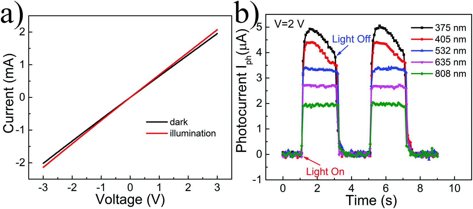 | ||
| Fig. 3 The photoelectric responses of the device based on hybrid suspended graphene-oxidized EGaIn nanoparticles. (a) Current–voltage plots of the device with and without light. The illumination is provided by a 532 nm laser with a power of 2 μW. The inset is a schematic of the composite structure of the suspended graphene and oxidized EGaIn nanoparticles. (b) Photocurrent responses of the device under the illumination of 375 nm, 405 nm, 532 nm, 635 nm and 808 nm lasers. The corresponding illumination powers are 2 μW, 14 μW, 20 μW, 36 μW and 27 μW, respectively. The applied bias is 2 V. | ||
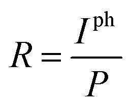
The dependences of the device photocurrent on laser power under irradiation of the abovementioned lasers are presented in Fig. 4a. In the logarithmic coordinate system, the photocurrent of the device increases linearly with the power. The relationship can be described as:
| Iph = A × Pα | (1) |
 | (2) |
 | (3) |
 | ||
| Fig. 4 (a) The relationship of photocurrent versus laser power for ultraviolet light (375 nm), visible light (405 nm, 532 nm and 635 nm) and near infrared light (808 nm). (b) The responsivity versus the laser power for five different lasers. (c) The relationship of external quantum efficiency (EQE) with wavelength. (d) The temporal response of the device. | ||
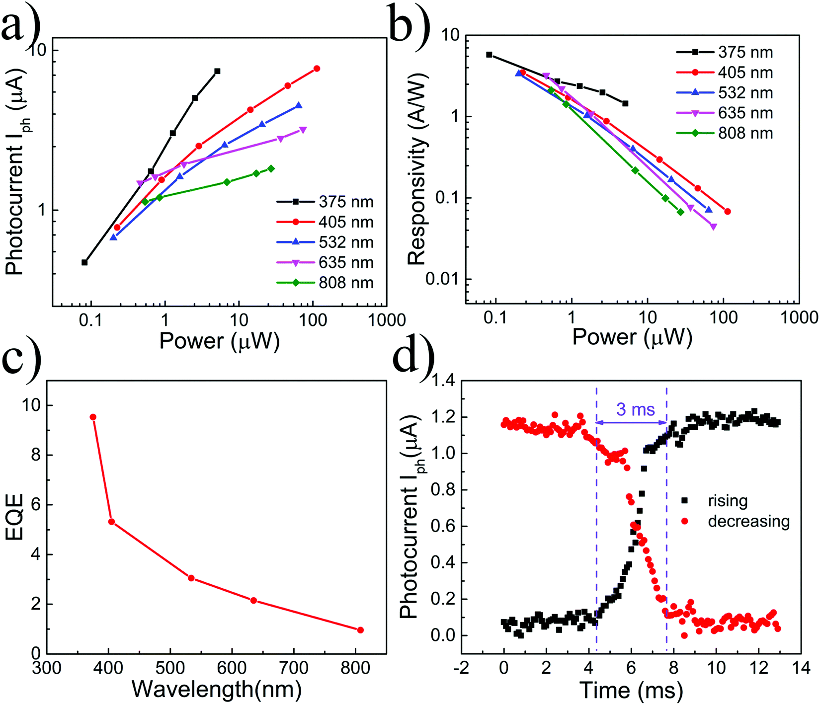
To study the response mechanism of the device, we further investigated the photo-response by changing the illumination. As shown in Fig. 5a, the 405 nm laser was used to illuminate the device from the top and the back, respectively, and the polarities and amplitudes of the corresponding light responses of the devices were completely different. The photocurrent of the device under the top light was basically the same as the response of pure PMMA-assisted suspended graphene (Fig. S7, ESI†), indicating that the slow photodesorption process of graphene dominates the generation of photocurrent. From the characterization in Fig. 2, we know that the oxidation of nanoparticles only occurs on the part exposed to the air. The part that contacts with graphene would still be metallic EGaIn because it is completely impermeable to all gases and liquids of graphene47 and because of the isolation of PMMA. The unoxidized core cannot absorb the light passing through the graphene film; therefore, its contribution to the photocurrent is small. The back light can be absorbed by the oxidized part of the nanoparticles due to its semiconducting properties. The carriers generated by the rapid photo-transition process form the photocurrent with the assistance of the graphene channel. The differences in responses prove that the oxide part is key to the generation of the photoelectric response. Next, the spatially resolved photocurrent response was measured with a focused laser beam (wavelength, 532 nm; spot size, ∼300 nm), as shown in Fig. 5b. Different from the previously reported graphene-based devices, where the photoelectric response is mainly generated at the interface between the graphene and metal contacts or in the vicinity of the PN junction,6 the photoelectric response of this device is generated in the large area where graphene and nanoparticles are composited, and the response amplitude of any position is basically the same. In addition, when the laser irradiates the substrate and the composite area, respectively, the differences of the photocurrent amplitude can exclude the possible influence of the substrate on the photocurrent, further confirming the importance of the nanoparticles.
 | ||
| Fig. 5 (a) The comparison of photocurrent responses under the illumination of top light and back light. The power is 1 μW. (b) The spatially resolved photocurrent responses of the device. The light source is 532 nm laser with a focused spot diameter of about 300 nm. The power is 2 μW. | ||
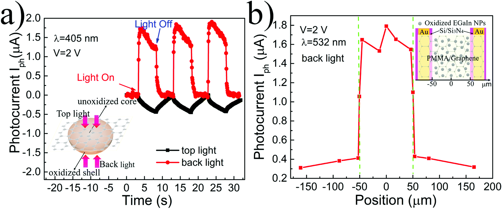
It has been proved that the oxidized EGaIn accounts for the enhancement of the opto-electric response. Therefore, it is necessary to investigate the reasons why oxidized EGaIn nanoparticles can achieve this enhancement in the broad waveband. The absorption spectrum of oxidized EGaIn nanoparticles is shown in Fig. 6. With the increase of the evaporation mass from 20 mg to 120 mg, the absorption intensity becomes larger. As the wavelength increases, the light absorption capacity gradually decreases, and the absorption in ultraviolet is stronger than that in the infrared band. On the one hand, the continuous and slow change of the absorption line, instead of the clear absorption edge, indicates that the energy band of the nanoparticles is not single and the waveband from ultraviolet to near infrared can be covered. On the other band, when the evaporation mass is 153 mg, the strongest absorption occurs at approximately 240 nm. When the evaporation mass is reduced to 120 mg, the strongest absorption position has a blue shift due to the quantum effect in size. This result indicates that the multiple sizes of the nanoparticles evaporated on the suspended graphene are helpful for diversification of the energy bands.
 | ||
| Fig. 6 The absorption of the oxidized EGaIn nanoparticles on the glass substrate. | ||
According to the previous test and characterization results, oxidized EGaIn nanoparticles can avoid the defects of the narrow absorption spectrum of general quantum dots and achieve broadband enhancement. We propose that the reasons may be as follows. First, along with the gradient change of oxygen element (from the outmost Ga2O3 layer to the innermost liquid metal), the energy band of the nanoparticles would change with the depth to achieve a smooth transition of the energy band from a large band gap (Ga2O3) to a bandgap of zero (metal),39 which is similar to ZnO nanostructures with changing oxygen content in the direction of the axis.48 Thus, various energy levels can be formed on a single nanoparticle. Second, the multi-size characteristics and related quantum effects in size and sub-oxides can adjust the position of the energy level and further increase the diversity of the energy level. The above main two factors result in the broadband absorption of nanoparticles. By compositing the graphene film, the ultra-high channel endows the carrier with a short transit time, achieving an enhancement in the photoelectric response from ultraviolet to near-infrared light.
It can be seen that the photodetector prepared with oxidized EGaIn nanoparticles and graphene achieves obvious enhancements in the responsivity, response time and response band. The device also breaks the short response band of the general quantum dot-based devices and has a simple structure and low manufacturing cost. In addition, it has been proved that the optoelectronic response of the device mainly comes from the oxide layer of EGaIn nanoparticles, and the method of increasing the thickness of the oxide layer can be used to further improve the performance. Importantly, the combination of element gradation and nanoparticles can broaden the response band of the quantum dot-based photodetector while obtaining a high response rate and fast response speed, which was confirmed in this work.
4. Conclusions
In summary, oxidized EGaIn was utilized to prepare nanoparticles on suspended graphene by a physical vapour deposition method. The nanoparticles are oxidized in the air, and the oxygen element forms a gradient distribution from outside to inside on a single nanoparticle. The suspended graphene compositing with oxidized EGaIn nanoparticles achieves great improvement in responsivity, response waveband and response speed due to the wide strong absorption of nanoparticles and great gain of the graphene channel. The responsivity is increased to about several A W−1 for a broad spectrum from ultraviolet to near-infrared light, while the response speed is 3 ms. This research reports a preliminary attempt toward the preparation and application of nanoparticles with gradient changes in elements and provides new ideas for the development of quantum dot-based optoelectronic devices.Conflicts of interest
There are no conflicts to declare.Acknowledgements
This work was partially supported by NSAF (grant no. U1730246), Education and Scientific Research Foundation for Young Teachers in Fujian Province (JAT200040) and the Research Fund Program of the State Key Laboratory of Low-Dimensional Quantum Physics (No. KF201704 and No. ZZ201703).References
- A. Serov, W. Steenbergen and F. De Mul, Opt. Lett., 2002, 27, 300–302 Search PubMed.
- A. M. Waxman, A. N. Gove, D. A. Fay, J. P. Racamato, J. E. Carrick, M. C. Seibert and E. D. Savoye, Neural Networks, 1997, 10, 1 Search PubMed.
- M. Geis, S. Spector, M. Grein, R. Schulein, J. Yoon, D. Lennon, S. Deneault, F. Gan, F. Kaertner and T. Lyszczarz, IEEE Photonics Technol. Lett., 2007, 19, 152–154 Search PubMed.
- S. R. Kim, H. K. Hong, C. H. Kwon, D. H. Yun, K. Lee and Y. K. Sung, Sens. Actuators, B, 2000, 66, 59–62 Search PubMed.
- G. F. Fine, L. M. Cavanagh, A. Afonja and R. Binions, Sensors, 2010, 10, 5469–5502 Search PubMed.
- Z. Sun and H. Chang, ACS Nano, 2014, 8, 4133–4156 Search PubMed.
- K. S. Novoselov, A. K. Geim, S. V. Morozov, D. Jiang, Y. Zhang, S. V. Dubonos, I. V. Grigorieva and A. A. Firsov, Science, 2004, 306, 666–669 Search PubMed.
- P. Avouris, Z. H. Chen and V. Perebeinos, Nat. Nanotechnol., 2007, 2, 605–615 Search PubMed.
- A. H. Castro Neto, F. Guinea, N. M. R. Peres, K. S. Novoselov and A. K. Geim, Rev. Mod. Phys., 2009, 81, 109–162 Search PubMed.
- Y. Cao, D. Rodan-Legrain, O. Rubies-Bigorda, J. M. Park, K. J. Watanabe, T. Taniguchi and P. Jarillo-Herrero, Nature, 2020, 583, 215–220 Search PubMed.
- X. S. Li, W. W. Cai, J. H. An, S. Kim, J. Nah, D. X. Yang, R. Piner, A. Velamakanni, I. Jung, E. Tutuc, S. K. Banerjee, L. Colombo and R. S. Ruoff, Science, 2009, 324, 1312–1314 Search PubMed.
- A. Reina, X. T. Jia, J. Ho, D. Nezich, H. B. Son, V. Bulovic, M. S. Dresselhaus and J. Kong, Nano Lett., 2009, 9, 30–35 Search PubMed.
- K. S. Kim, Y. Zhao, H. Jang, S. Y. Lee, J. M. Kim, K. S. Kim, J. H. Ahn, P. Kim, J. Y. Choi and B. H. Hong, Nature, 2009, 457, 706–710 Search PubMed.
- X. S. Li, Y. W. Zhu, W. W. Cai, M. Borysiak, B. Y. Han, D. Chen, R. D. Piner, L. Colombo and R. S. Ruoff, Nano Lett., 2009, 9, 4359–4363 Search PubMed.
- X. Wang, L. J. Zhi and K. Mullen, Nano Lett., 2008, 8, 323–327 Search PubMed.
- Y. Liu, R. Cheng, L. Liao, H. Zhou, J. Bai, G. Liu, L. Liu, Y. Huang and X. Duan, Nat. Commun., 2011, 2, 579 Search PubMed.
- T. Mueller, F. Xia and P. Avouris, Nat. Photonics, 2010, 4, 297–301 Search PubMed.
- T. J. Echtermeyer, L. Britnell, P. K. Jasnos, A. Lombardo, R. V. Gorbachev, A. N. Grigorenko, A. K. Geim, A. C. Ferrari and K. S. Novoselov, Nat. Commun., 2011, 2, 1–5 Search PubMed.
- B. Zhao, J. M. Zhao and Z. M. Zhang, Appl. Phys. Lett., 2014, 105, 031905 Search PubMed.
- M. Furchi, A. Urich, A. Pospischil, G. Lilley, K. Unterrainer, H. Detz, P. Klang, A. M. Andrews, W. Schrenk, G. Strasser and Y. Mueller, Nano Lett., 2012, 12, 2773–2777 Search PubMed.
- X. T. Gan, K. F. Mak, Y. D. Gao, Y. M. You, J. Hone, T. F. Heinz and D. Englund, Nano Lett., 2012, 12, 5626–5631 Search PubMed.
- G. Konstantatos, M. Badioli, L. Gaudreau, J. Osmond, M. Bernechea, F. P. G. De Arquer, F. Gatti and F. H. L. Koppen, Nat. Nanotechnol., 2012, 7, 363–368 Search PubMed.
- Z. H. Sun, Z. K. Liu, J. H. Li, G. A. Tai, S. P. Lau and F. Yan, Adv. Mater., 2012, 24, 5878–5883 Search PubMed.
- W. H. Guo, S. G. Xu, Z. F. Wu, N. Wang, M. M. T. Loy and S. W. Du, Small, 2013, 9, 3031–3036 Search PubMed.
- M. Kataria, K. Yadav, G. Haider, Y. M. Liao, Y. R. Liou, S. Y. Cai, H. I. Lin, Y. H. Chen, C. R. P. Inbaraj, K. P. Bera, H. M. Lee, Y. T. Chen, W. H. Wang and Y. F. Chen, ACS Photonics, 2018, 5, 2336–2347 Search PubMed.
- S. M. Yadav and A. Pandey, IEEE Trans. Electron Dev., 2019, 66, 3417–3424 Search PubMed.
- K. P. Bera, G. Haider, Y. T. Huang, P. K. Roy, C. R. P. Inbaraj, Y. M. Liao, H. I. Lin, C. H. Lu, C. Shen, W. Y. Shih, W. H. Shih and Y. F. Chen, ACS Nano, 2019, 13, 12540–12552 Search PubMed.
- P. Y. Ren, W. Hu, Q. L. Zhang, X. L. Zhu, X. L. Zhuang, L. Ma, X. P. Fan, H. Zhou, L. Liao, X. F. Duan and A. L. Pan, Adv. Mater., 2014, 26, 7444–7449 Search PubMed.
- L. W. Yin and S. T. Lee, Nano Lett., 2009, 9, 957–963 Search PubMed.
- C. Y. He, Q. A. Wu, X. Z. Wang, Y. L. Zhang, L. J. Yang, N. Liu, Y. Zhao, Y. N. Lu and Z. Hu, ACS Nano, 2011, 5, 1291–1296 Search PubMed.
- F. X. Gu, Z. Y. Yang, H. K. Yu, J. Y. Xu, P. Wang, L. M. Tong and A. L. Pan, J. Am. Chem. Soc., 2011, 133, 2037–2039 Search PubMed.
- Z. Y. Yang, J. Y. Xu, P. Wang, X. J. Zhuang, A. L. Pan and L. M. Tong, Nano Lett., 2011, 11, 5085–5089 Search PubMed.
- L. Li, H. Lu, Z. Y. Yang, L. M. Tong, Y. Bando and D. Golberg, Adv. Mater., 2013, 25, 1109–1113 Search PubMed.
- O. Takahisa, N. Katsuhiro and O. Y. Matsuo, J. Appl. Phys., 2009, 105, 073106 Search PubMed.
- M. D. Dickey, Adv. Mater., 2017, 29, 1606425 Search PubMed.
- J. Cutinho, B. S. Chang, S. Oyola-Reynoso, J. Chen, S. S. Akhter, I. D. Tevis, N. J. Bello, A. Martin, M. C. Foster and M. M. Thuo, ACS Nano, 2018, 12, 4744–4753 Search PubMed.
- W. Y. Kong, G. A. Wu, K. Y. Wang, T. F. Zhang, Y. F. Zou, D. D. Wang and L. B. Luo, Adv. Mater., 2016, 28, 10725–10731 Search PubMed.
- T. Liu, P. Sen and C. J. Kim, J. Microelectromech. Syst., 2012, 21, 443–450 Search PubMed.
- P.-F. Wang, Q. Hu, B. Lv, J.-L. Zhu, W. Ma, Z. Dong, J. Wei and J.-L. Sun, Nanotechnology, 2020, 21, 145703 Search PubMed.
- T. R. Lear, S. H. Hyun, J. W. Boley, E. L. White, D. H. Thompson and R. K. Kramer, EML, 2017, 13, 126–134 Search PubMed.
- T. Liu, P. Sen and C. J. Kim, J. Microelectromech. Syst., 2012, 21, 443–450 Search PubMed.
- D. Graf, F. Molitor, K. Ensslin, C. Stampfer, A. Jungen, C. Hierold and L. Wirtz, Nano Lett., 2007, 7, 238–242 Search PubMed.
- N. Wada, S. A. Solin, J. Wong and S. Prochazka, J. Non-Cryst. Solids, 1981, 43, 7–15 Search PubMed.
- S. Berciau, S. Ryu, L. E. Brus and T. F. Heinz, Nano Lett., 2009, 9, 346–352 Search PubMed.
- S. Liu, S. N. Reed, M. J. Higgins, M. S. Titus and R. Kramer-Bottiglio, Nanoscale, 2019, 11, 17615–17629 Search PubMed.
- Y. Y. Hsu, C. Y. Lin, Y. C. Lai, K. R. Wu, K. K. Ng, C. S. Chang, G. C. Chi, P. C. Yu and F. S. S. Chien, Opt. Express, 2015, 23, 14344–14350 Search PubMed.
- P. Z. Sun, Q. Yang, W. J. Kuang, Y. V. Stebunov, W. Q. Xiong, J. Yu, R. R. Nair, M. I. Katsnelson, S. J. Yuan, I. V. Grigorieva, M. Lozada-Hidalgo, F. C. Wang and A. K. Geim, Nature, 2020, 579, 229–232 Search PubMed.
- J. Wang, Z. Wang, B. Huang, Y. Ma, Y. Liu, X. Qin, X. Zhang and Y. Dai, ACS Appl. Mater. Interfaces, 2012, 4, 4024–4030 Search PubMed.
Footnote |
| † Electronic supplementary information (ESI) available: The composite structure of EGaIn nanoparticles and supported graphene on the Si3N4 substrate, the magnified Raman spectrum of supported graphene and suspended graphene, the gradient change of element content within the oxide layer, the detailed manufacturing process of device, the photoelectric response of prepared device in the vacuum, the characterization of stability in device's performance and preparation method, control experiments of PMMA/graphene, oxidized EGaIn nanostructures and composite structure. See DOI: 10.1039/d1ma00318f |
| This journal is © The Royal Society of Chemistry 2021 |