
 Open Access Article
 This Open Access Article is licensed under a Creative Commons Attribution-Non Commercial 3.0 Unported Licence
Unraveling the compositional heterogeneity and carrier dynamics of alkali cation doped 3D/2D perovskites with improved stability†
Ming-Chun
Tang‡
 *abc,
Siyuan
Zhang‡
ad,
Timothy J.
Magnanelli
a,
Nhan V.
Nguyen
a,
Edwin J.
Heilweil
a,
Thomas D.
Anthopoulos
*b and
Christina A.
Hacker
*a
*abc,
Siyuan
Zhang‡
ad,
Timothy J.
Magnanelli
a,
Nhan V.
Nguyen
a,
Edwin J.
Heilweil
a,
Thomas D.
Anthopoulos
*b and
Christina A.
Hacker
*a
aPhysical Measurement Laboratory, National Institute of Standards and Technology (NIST), Gaithersburg, MD 20899, USA. E-mail: mingchun.tang@nist.gov; chistina.hacker@nist.gov
bKing Abdullah University of Science and Technology (KAUST), KAUST Solar Center (KSC), and Physical Science and Engineering Division (PSE), Thuwal, 23955-6900, Saudi Arabia. E-mail: thomas.anthopoulos@kaust.edu.sa
cInstitute for Research in Electronics and Applied Physics & Maryland NanoCenter, University of Maryland, College Park, MD 20742, USA
dTheiss Research, La Jolla, CA 92037, USA
First published on 11th December 2020
Abstract
Preventing the degradation of hybrid perovskites by humid air remains a challenge for their future commercial utilization. 3D/2D perovskites with hierarchical architecture have attracted significant attention due to their promising power conversion efficiency (PCE) and device stability. Here, we report a novel 3D/2D planar bi-layer perovskite obtained by growing a 2D Ruddlesden–Popper layer on top of a 3D rubidium (Rb+)-doped triple-cation perovskite. Rb+ cation incorporation decreases the work function, and 3D/2D films show smaller work function values compared to classic 3D perovskites. X-ray photoemission spectroscopy (XPS) confirms the presence of a 2D perovskite capping layer and observes halide migration. Time-resolved terahertz spectroscopy (TRTS) shows that the average DC carrier mobility for the 3D/2D hierarchical structures and their 3D counterparts is one order of magnitude higher than that for the 2D perovskite. The resulting 3D/2D Rb+-incorporated perovskite solar cells show a peak PCE of >20%, which is slightly higher than their 3D counterparts (19.5%). Benefiting from moisture resistivity, the 3D/2D perovskite photovoltaics show significantly improved long-term stability by retaining 81% of the initial PCE after 60 days of exposure to ambient air (50 ± 10% relative humidity) without encapsulation, highlighting the potential of engineered stable 3D/2D perovskite solar cells for their commercial utilization.
Introduction
Hybrid organic–inorganic metal-halide perovskites prepared via low-cost solution-processing approaches have aroused tremendous research interest due to their remarkable optoelectronic properties.1–6 Substantial efforts have been put into improving the device power conversion efficiency (PCE),7 which is positively related to the perovskite morphology, microstructure, mobility, defects, and trap state density.8–13 To date, planar heterojunction three-dimensional (3D) perovskite photovoltaics fabricated through interfacial engineering have recently surpassed the PCE milestone of 25%.14 Despite their high efficiency, 3D perovskites are susceptible to the external environment, such as moisture, heat, and irradiation, which leads to phase degradation and hinders the device performance.15–17In contrast to their 3D counterparts, two-dimensional (2D) Ruddlesden–Popper layered perovskites have recently gained extensive attention because of their tunability of the optoelectronic properties and, more importantly, ambient stability.18–20 2D layered perovskites have a general formula of R2An−1MnX3n+1, where R+ is a bulky organic cation such as butylammonium and phenylethylammonium (PEA+), A+ represents smaller organic or inorganic cations, including methylammonium (MA+) or formamidinium (FA+), and n is the number of 3D inorganic corner-sharing PbI64− octahedra layers separated by bulky organic layers. M2+ metal cations are typically lead (Pb2+) or tin (Sn2+), and X− is a monovalent halide anion such as chloride (Cl−), bromide (Br−), iodide (I−), or a mixture.21–23 The hydrophobic spacing layer and the densely-packed crystal structure prevent direct contact of 2D layered perovskites with moisture. Therefore, 2D perovskite solar cells could remain stable for thousands of hours in an ambient environment. Based on the benefits of superior stability, these 2D perovskites were further incorporated onto the surface of 3D counterparts as a capping layer to promote the stability of the underneath 3D perovskite phase without significant compromise of the device performance.24 For instance, 3D/2D heterojunction solar cells were constructed based on PEA2MA4Pb5I16 and a 3D classic MAPbI3 perovskite, which showed enhanced device stability toward exposure to 75% relative humidity (RH).25 Recently, Nazeeruddin et al. reported that the use of 2D layered perovskites had been extended to a cesium (Cs+)-incorporated 3D mixed-cation and mixed-halide perovskite with an average PCE of 20.1% based on a PEA2PbI4/Cs0.1FA0.74MA0.13PbI2.48Br0.39 stacked structure, which retained 85% of the initial device performance for 800 h at 50 °C.26 Other bulky organic ligands have also been introduced into 3D/2D heterojunction photovoltaics, resulting in decent PCE with enhanced device stability.19,27 However, despite the achievement of stable and high-performance solar cells with improved stability, the in-depth roles of the 2D layer and alkali cations in the electronic structure, chemical composition, and carrier dynamics in 3D/2D hybrid systems are still not yet fully developed.
Herein, we report the comprehensive analysis of the electronic structure, chemical compositions, and carrier dynamics of rubidium (Rb+)-incorporated FA0.85−xMA0.15RbxPbI2.55Br0.45 (x = 0 and 0.05, abbreviated as M0 and Rb5, respectively) with a layered PEA2Pb(IyBr1−y)4 capping layer 3D/2D heterojunction perovskites. X-ray diffraction (XRD) patterns show characteristic peaks and well-preserved crystallinity of the 3D/2D bi-layer perovskites. Benefiting from the hydrophobicity of the PEA2Pb(IyBr1−y)4 layer, the 2D perovskite prevents moisture penetration into the 3D perovskite. Ultraviolet photoelectron spectroscopy (UPS) characterization shows that Rb+ alkali metal cation doping decreases the work function, and the 3D/2D perovskites exhibit smaller work function values compared to their classic 3D counterparts. X-ray photoemission spectroscopy (XPS) confirms the presence of a 2D PEA2Pb(IyBr1−y)4 layer, and the XPS depth profile observes halide migration in the 3D/2D perovskite architecture. Through time-resolved terahertz measurements, the average non-contact DC carrier mobility for the pure 2D PEA2PbI4 perovskite was 1.3 and 1.7 (cm2 V−1 s−1) using 400 nm and 800 nm excitation wavelengths, respectively, whereas the 3D/2D hierarchical perovskite (i.e., Rb5/2D) yielded average DC mobility values of 14.9 and 45.5 (cm2 V−1 s−1). These differences were reflected in the photovoltaic performance: slightly higher average PCEs were demonstrated with 3D/2D perovskite solar cells (≈19.5% for Rb5/2D) than their 3D counterparts (≈18.6% for Rb5). With the advantage of moisture resistivity, the 3D/2D (i.e., Rb5/2D) perovskite photovoltaics show significantly improved long-term stability, with the initial PCE decreasing by only 19% after exposure to ≈50% RH at room temperature for 60 days without encapsulation. By comparison, the control 3D sample (i.e., Rb5) underwent a significant decrease of 65% in the PCE. This vital information and understanding of the electronic structure, carrier dynamics, and composition of 3D/2D heterojunction perovskites with Rb+ addition can be used to guide the synthesis of new 3D/2D perovskite films to improve the performance and stability in optoelectronic applications.
Results and discussion
Formation and impact of 3D/2D heterostructure perovskites
The device configuration used in this study is based on the following architecture of glass/indium-doped tin oxide (ITO)/compact titanium dioxide (c-TiO2)/3D perovskite/2D layered perovskite/2,2′,7,7′-tetrakis-(N,N-di-pmethoxyphenylamine)-9,9′-spirobifluorene (Spiro-OMeTAD)/gold (Au), as illustrated in Fig. 1a. The 3D FA+-dominated perovskite films of FA0.85−xMA015RbxPbI2.55Br0.45 (x = 0 and 0.05), abbreviated as M0 and Rb5, respectively, were processed through a one-step spin-coating antisolvent assisted method,28 leading to a compact and pinhole-free perovskite layer with a thickness of ≈400 nm, confirmed by profilometry and spectroscopic ellipsometry measurements (Fig. S1, ESI†). Through spin casting a PEAI solution upon the annealed 3D perovskite film, a 2D layered PEA2Pb(IyBr1−y)4 perovskite (abbreviated as 2D) was formed by PEAI reacting with excess and unreacted lead halides or diffusing into the polycrystalline 3D perovskite via grain boundaries and the surface.29,30 The thickness of the 2D perovskite PEA2Pb(IyBr1−y)4 capping layer can be tuned by varying the concentration of the PEAI solution (1, 5, and 10 mg mL−1 in isopropanol). A schematic representation of the preparation process of both 3D and 3D/2D heterostructure perovskite layers is shown in Fig. S2 (ESI†). Unless stated otherwise, all the characterization results of the 3D/2D perovskite were based on the optimized 2D layered perovskite fabricated using 5 mg mL−1 PEAI solution. | ||
| Fig. 1 (a) A schematic diagram of representative 3D/2D heterostructure perovskite solar cells used in this work together with representative 3D/2D perovskite films. (b) Optical absorbance spectra and (c) XRD patterns of 2D layered PEA2PbI4, 3D M0 and Rb5, and 3D/2D heterostructure perovskite films. (d) The contact angle of water and photographs on Rb5 and Rb5/2D perovskite films. | ||
The optical energy band gaps of 3D and 3D/2D perovskite films were calculated from the Tauc plot (Fig. S3, ESI†) from the ultraviolet-visible (UV-vis) absorption spectra (Fig. 1b). All the 3D films (M0 and Rb5) and their corresponding 3D/2D perovskites (M0/2D and Rb5/2D) show similar absorption profiles that have a broad absorption band over the entire visible region with two characteristic peaks located at ≈780 nm and ≈480 nm. On the other hand, the optical UV-vis absorption spectrum of the 2D PEA2PbI4 layered perovskites shows typical features of a high-energy continuum absorption edge and a lower-energy excitonic peak. The optical band gaps appear to remain similar between the 3D and 3D/2D perovskite films, which is consistent with earlier reports of multidimensional hybrid perovskites.19,31
Fig. 1c shows XRD patterns of perovskite thin films based on 2D perovskite PEA2PbI4, the 3D perovskites (M0 and Rb5), and the 3D/2D perovskites (M0/2D and Rb5/2D). The crystal structure of the pristine 2D PEA2PbI4 perovskite films shows peaks at 5.4°, 10.8°, and 16.3°, which can be assigned to the scattering from the (002), (004), and (006) diffraction plane of the layered perovskite PEA2PbI4, respectively.29 Based on the (002) reflection peaks of PEA2PbI4, the distance between the 2D perovskite layers is calculated to be 16.35 Å, and the growth planes are primarily parallel to the substrate.32 The XRD patterns of M0 and Rb5 show typical peaks for the black perovskite α phase at 14.1° in the polycrystalline 3D perovskite films. For the 3D/2D perovskite films, all the characteristic peaks can be indexed to the 3D and 2D perovskites, indicating the well-preserved crystallinity of the 3D/2D planar heterostructure in these perovskite stacked layers. Moreover, XRD patterns of other 3D/2D perovskite films with different PEAI solution concentrations (1, 5, and 10 mg mL−1 in isopropanol) of the 2D perovskite capping layers are also shown (Fig. S4a, ESI†). The XRD pattern of the Rb5/2D heterojunction perovskites remains similar to the Rb5 film when using 1 mg mL−1 PEAI solution, indicating that the 2D perovskite is not formed. When employing the 5 and 10 mg mL−1 PEAI solutions, the (002) reflection peak of the 2D perovskite becomes more dominant.
Contact angle tests were performed to elucidate the 2D capping layer's effect to suppress moisture diffusion (Fig. 1d). The pristine 3D Rb5 perovskite film shows a ≈55.6° contact angle, while the capping layer treated 3D/2D perovskite film shows a contact angle of 89.7°. The higher contact angle suggests that the 2D capping layers have high water resistance and act as a protective coating against moisture, preserving the underlying 3D Rb5 perovskite layer. Therefore, the 3D/2D films exhibit stronger water resistance and show a more hydrophobic surface. The optical images of the Rb5 and Rb5/2D films (Fig. 1d) show that both films appear black, indicating desirable and complete perovskite conversion.
Electronic structures of the 2D, 3D, and 3D/2D heterostructure perovskites
Even though the absorption spectra of the 3D/2D stacked perovskite show similar profiles to their classic 3D counterparts, the UPS results demonstrate that the electronic structure at the 3D/2D films’ surface differs from the 3D perovskites. Fig. 2a shows the secondary electron edge (SEE) and the low binding energy regions of the UPS spectra for the pure 2D, 3D, and 3D/2D bi-layer perovskites. All energies are referenced to a standard Fermi level (Ef = 0 eV), calibrated using sputter-cleaned Au. The work function (WF) was determined by the difference between the UV photons (21.21 eV) and the binding energy of the SEE. The conduction band minimum (CBM) position, ECBM, is calculated from the position of the valence band maximum (VBM) and the bandgap value. The determination of these perovskite films’ energy levels can unravel the role of band alignment in charge transport. The Fermi level is close to the CBM, indicating that all these perovskite films function as an n-type semiconductor. As shown in Fig. 2b, the work functions of the classic 2D PEA2PbI4 and 3D films (i.e., M0 and Rb5) were determined to be 4.33 ± 0.03 eV, 4.73 ± 0.03 eV, and 4.53 ± 0.04 eV, respectively, as determined by a linear extrapolation of the secondary electron cutoff. The addition of Rb+ alkali metal cations in Rb5 decreases the WF and shifts both the VBM and CBM to a higher level compared with M0. Upon capping with a 5 mg mL−1 PEAI solution, the WFs of M0/2D (≈4.48 eV) and Rb5/2D (≈4.28 eV) exhibit smaller values compared with their pure 3D counterparts, and the band edges in the 3D/2D perovskite films are upshifted by ≈0.04 eV and ≈0.09 eV in M0/2D and Rb5/2D, respectively. The trends observed here are in good agreement with literature reports.33,34 3D/2D bi-layer perovskite films with various PEAI solution concentrations were also investigated (see Fig. S5, ESI†), and the work function gradually decreases as the PEAI solution concentration increases (1 mg mL−1 to 10 mg mL−1). The detailed evolution of the UPS spectra and the standard deviation from averaging the results obtained with different samples and spots are summarized in the ESI† (Table S1). The energy levels of the 3D/2D perovskites were in good agreement with the charge transport layers (TiO2 and Spiro-OMeTAD in this case), which could facilitate charge transfer and suppress charge recombination.35,36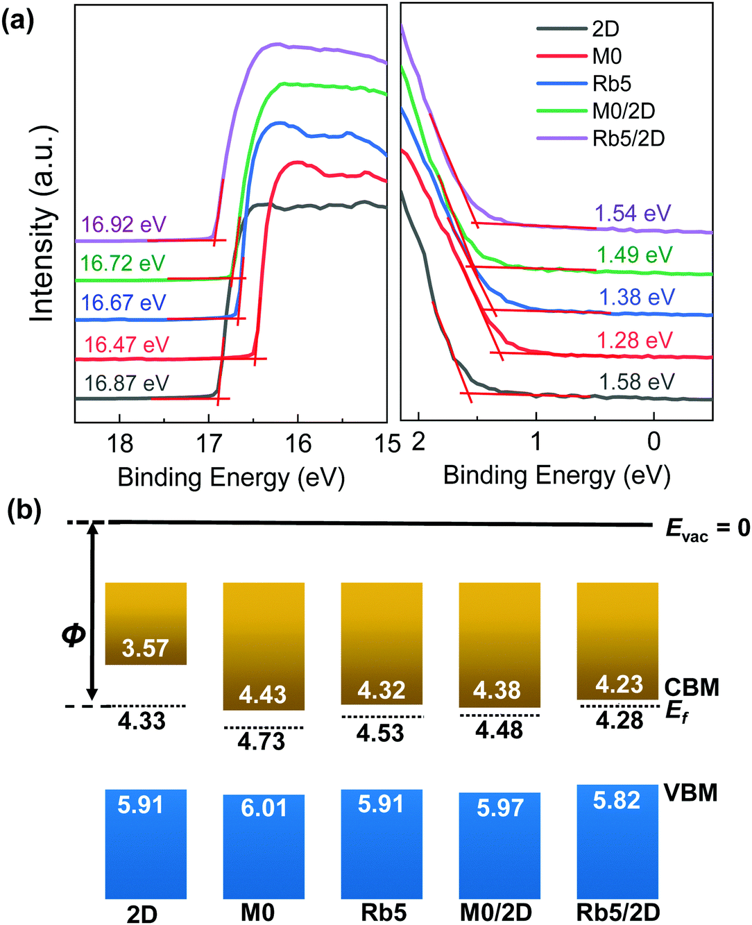 | ||
| Fig. 2 (a) UPS secondary electron edge (SEE) and the low binding energy region (near the Fermi energy EF = 0 eV) of the classic 2D, 3D, and 3D/2D bi-layer perovskites. The onset of ionization of filled states relative to zero binding energy is used to track the shifts of EF relative to the VBM. (b) Schematics of the electronic structure of the 2D, 3D, and 3D/2D bi-layer perovskite films. | ||
Confirmation of the 2D layered perovskite on 3D perovskites via X-ray photoemission spectroscopy
To further verify the 2D perovskite layer's presence on 3D perovskites, XPS measurements were carried out on the classical 2D, 3D, and 3D/2D perovskite films as shown in Fig. 3. The C 1s core-level spectrum (Fig. 3a) of the pristine 2D PEA2PbI4 perovskite film contains three components which are consistent with a previous report: the ≈284.6 eV component is assigned to surface absorbed amorphous carbon (C–C), the ≈286.2 eV peak is attributed to the C–N bond in PEAI, and the peak at a binding energy of ≈291.7 eV is assigned to the π–π* shakeup satellite peak for carbon in aromatic systems, the phenyl functional group in the PEA+ cation, in this case. The kinetic energy of the emitted photoelectrons from carbon is reduced due to the delocalized aromatic π system. The presence of this satellite peak confirms the presence of the 2D perovskite layer. The C 1s spectrum of the pristine 3D perovskite film also consists of three components, peaks at 284.6 eV, 286.2 eV, and 288.2 eV, which can be attributed to C–C, C–N, and C![[double bond, length as m-dash]](https://www.rsc.org/images/entities/char_e001.gif) N, respectively. The FA+ and MA+ cations are confirmed by the presence of the peaks for C–N and CN bonding. In other 3D/2D perovskite films, the Rb5 film processed with 1 mg mL−1 of the PEAI solution still shows similar features to the classic 3D Rb5 perovskite film (see Fig. S6a, ESI†). This observation is consistent with the XRD results. As the PEAI solution concentration increased to 5 mg mL−1 and 10 mg mL−1, the 2D perovskite features became more pronounced, where the π–π* shakeup satellite peak increases accompanied by the decrease of CN from the FA+ cation (Fig. S6, ESI†). This observation is consistent with the increased thickness of the 2D perovskite layer in the 3D/2D perovskite heterostructure. This phenomenon was also confirmed by the N 1s spectra, as shown in Fig. 3b. The bonds of C–N (401.9 eV) and CN (400.3 eV) from the FA+ cation can be observed in the N 1s spectrum of pristine 3D (i.e., M0 and Rb5), while the classic 2D PEA2PbI4 perovskite film only shows one bond feature of C–N (401.9 eV). Fig. S6 (ESI†) shows that the 2D perovskite peak at higher binding energy became more dominant as the PEAI solution concentration increases, indicating a thicker 2D perovskite film.
N, respectively. The FA+ and MA+ cations are confirmed by the presence of the peaks for C–N and CN bonding. In other 3D/2D perovskite films, the Rb5 film processed with 1 mg mL−1 of the PEAI solution still shows similar features to the classic 3D Rb5 perovskite film (see Fig. S6a, ESI†). This observation is consistent with the XRD results. As the PEAI solution concentration increased to 5 mg mL−1 and 10 mg mL−1, the 2D perovskite features became more pronounced, where the π–π* shakeup satellite peak increases accompanied by the decrease of CN from the FA+ cation (Fig. S6, ESI†). This observation is consistent with the increased thickness of the 2D perovskite layer in the 3D/2D perovskite heterostructure. This phenomenon was also confirmed by the N 1s spectra, as shown in Fig. 3b. The bonds of C–N (401.9 eV) and CN (400.3 eV) from the FA+ cation can be observed in the N 1s spectrum of pristine 3D (i.e., M0 and Rb5), while the classic 2D PEA2PbI4 perovskite film only shows one bond feature of C–N (401.9 eV). Fig. S6 (ESI†) shows that the 2D perovskite peak at higher binding energy became more dominant as the PEAI solution concentration increases, indicating a thicker 2D perovskite film.
 | ||
| Fig. 3 Representative XPS core-level spectra of (a) C 1s and (b) N1s of the classical 2D PEA2PbI4, M0, Rb5, and Rb5/2D perovskite films. The y-axis is on a log scale to facilitate the view of the low-intensity peak. | ||
Distribution of chemical components throughout the pure 3D and 3D/2D perovskites
To further analyze the distribution of chemical components throughout the films, depth-profile XPS was conducted for pure 3D and 3D/2D perovskite films. The interfacial region between the perovskite film and substrate was determined by an abrupt decrease of the Pb 4f signal accompanied by the increase of the O 1s and In 3d signals from the ITO substrate. The film thicknesses were measured by profilometry and ellipsometry (as shown in Fig. S1, ESI†). Fig. 4 illustrates the 3D/2D perovskite film (i.e., Rb5/2D) elemental composition as a function of the depth profile collected using XPS by using in situ Ar+ sputtering. To compare with its 3D counterpart, the depth-profile XPS of the Rb5 perovskite film is also shown in Fig. S7 and S8 (ESI†). The sputtering time was converted to the sampling depth with the assumption that the etching rate was constant. Fig. 4a shows the XPS spectra in the 80 eV to 10 eV range covering the Br 3d (70–67 eV), I 4d (53–47 eV), and Pb 5d (24–18 eV) core levels. This representation's practical advantage is that information from bromide, iodide, and lead is acquired in the same spectral window, giving an accurate relative intensity ratio at a specific probing depth, which can be easily compared without laborious calculations. As shown in Fig. 4a, both I and Br are observed on the surface of the 3D/2D perovskite layer. | ||
| Fig. 4 (a) XPS depth profiling in the 80–10 eV range covering the Br 3d, I 4d, and Pb 5d core level peaks in the Rb5/2D film. The figure at the top presents the spectrum in the 80–10 eV range on the surface of the sample (depth = 0 nm). (b) XPS depth profiling of Rb 3d in the Rb5/2D film. The top figure presents the core level peak of Rb 3d inside the sample at 100 nm depth. (c) The atomic ratios of the halides and metal cations relative to lead Pb2+ in Rb5/2D. Error bars indicate the standard deviation from averaging the results obtained with different spots. | ||
Fig. 4b shows the XPS depth profiling of Rb 3d in the Rb5/2D film. Rb 3d is not initially detected on the film surface. Then a gradual increase of the intensity is observed after the first sputtering, confirming that the Rb+ alkali metal cation doping is limited to the 3D region and Rb+ does not migrate into the 2D layer. To better present the film composition, the atomic ratio of halides (I 3d and Br 3d) and metal cations Rb+ (Rb 3d) is normalized to lead Pb2+ (Pb 4f) for Rb5/2D and summarized in Fig. 4c. As shown in Fig. 4c, the Rb/Pb ratio is close to 0 on the top surface of the Rb5/2D film, while the I/Pb and Br/Pb ratios are ≈3.3 and ≈0.5, respectively. As the depth increases into the 3D portion, the Rb/Pb ratio increases slightly to ≈0.03, and then ≈0.05 as the sputtering time increases. Both the I/Pb and Br/Pb ratios, on the other hand, decrease to ≈2.3 and ≈0.2 after the first sputtering, and then increase to ≈2.6 and ≈0.3 within the film as the depth increases. The drastic decrease of the halide to lead (X/Pb) ratio after the first sputtering is consistent with the 2D layer transition, where X/Pb is supposed to be 4, to the 3D portion of the film, where X/Pb is close to 3. Here, as the PEAI solution is spin-coated on the top of the 3D layers, the PEAI molecules diffuse into the polycrystalline structure of the 3D layer through surface and grain boundaries, reacting with the 3D perovskite and excess lead halide, forming the 3D/2D stacked structures. The X/Pb value (I/Pb + Br/Pb) in the 3D region increases from ≈2.5 to ≈2.9 as the depth increases. This may be attributed to halide migration from the 3D into the 2D layer at the 3D/2D interface. The profiles for M0, Rb5, and M0/2D are also presented in the ESI† (Fig. S8). The X/Pb ratios in M0/2D (Fig. S8c, ESI†) show a similar pattern compared to Rb5/2D, where halides migrate from the 3D layer into the 2D perovskite, which leads to an inhomogeneous halide distribution to a more significant extent. Compared with the non-doped 3D counterparts (Fig. S8a and b, ESI†), a small amount of alkali metal (Rb+) cations effectively prevented halide segregation in the mixed-cation and mixed-halide perovskite, which functions similarly to the addition of Cs+ cations reported previously.37 This is the first report of the direct observation of halide migration from a 3D into a 2D perovskite at the 3D/2D interface using XPS depth profiling. This is unique compared with other previous work, mostly using optical or electrical techniques to characterize the halide migration and not having spatial composition distribution information.
Carrier dynamics of pure 2D, 3D, and 3D/2D hierarchical structures studied via time-resolved terahertz spectroscopy
Time-resolved terahertz (THz) spectroscopy (TRTS) was employed to interrogate the charge carriers’ localized mobility following photoexcitation. Each perovskite sample was photoexcited using 400 nm pulses to generate charge carriers and monitored by subsequent THz probe pulse absorption to provide information on their ultrafast characteristics and dynamics. Here, we fit THz probe frequency-dependent complex photo-responses (TRTS measurements, see Fig. 5a) using a rebounding carrier model (Drude–Smith, eqn (1)38) to assess the dielectric response and extract the total charge mobility of each perovskite sample. The Drude–Smith model, eqn (1), represents the simplest way to model the photoinduced dielectric response of charge carriers that are subject to confinement. Here, Cσ represents a conductive prefactor (including the carrier number density ΔN, and effective mass m*), τ the charge scattering time, and c1 the backscattering parameter, roughly the proportion of charges that rebound, ranging from none to all as c1 = 0 to −1. The real and imaginary components were fit simultaneously with individual frequencies weighted by their relative magnitudes in the incident (unabsorbed) THz probe. | (1) |
 | ||
| Fig. 5 TRTS data collected using 1.25 mJ cm−2, 400 nm photoexcitation and a 5 ps time delay between UV photoexcitation and the THz probe. (a) Frequency-dependent complex TRTS responses for 2D layered PEA2PbI4, 3D M0 and Rb5, and 3D/2D heterostructure perovskite solid-state films. Circles/solid line fits and squares/dashed line fits represent the total mobility's real and imaginary components (converted from the photoinduced dielectric response), respectively. (b) Resulting μDC (zero-frequency limit of the real mobility in (a)) and μTHz (average of the real part over the data range of 0.5 THz to 2 THz) extracted for each dataset. The error bars in (b) indicate 95% confidence intervals (type A k = 1.96 analysis) for each extracted mobility value. | ||
Photovoltaic device performance and stability
It has generally been accepted that the solution chemistry in perovskite formulations, together with the processing protocols, can both impact the morphology of the final thin film. To better understand the impacts of Rb+ incorporation and the 2D layered perovskite capping layer, we studied the morphology for 3D (i.e., M0 and Rb5) and 3D/2D (i.e., M0/2D and Rb5/2D) perovskite solid-state thin films via scanning electron microscopy (SEM) as shown in Fig. S10 (ESI†). Unlike the M0/2D (without Rb+ doping) layers, where we see an increasing number of pinholes and cracks in the perovskite crystals with the 2D perovskite layer (Fig. S10c and d, ESI†), the Rb5/2D heterostructure tends to form high quality and continuous perovskite layers comprised of compact domains. For comparison, the top-view SEM images of the M0 and Rb5 perovskites without the 2D perovskite capping layer are also shown in Fig. S10a and b (ESI†). The layer morphology differences may be attributed to the complex perovskite crystal nucleation and growth rate and interaction between various precursors within the colloidal solution, including solvents and solutes. Therefore, we could obtain high quality and full coverage perovskite layers through careful design of the perovskite formulations. These features are expected to benefit the performance of perovskite solar cells, which will be discussed later.To demonstrate the device performance, we fabricated planar n–i–p type 2D layered PEA2PbI4, 3D M0 and Rb5, and 3D/2D heterostructure perovskite solar cells with a layer configuration (see Fig. 1a). We first collected and compared data on 20–25 solar cells based on these types of perovskite films with the statistical distribution of the PCE (see Fig. 6a) as summarized in Table S2 (ESI†). Representative J–V curves of the peak PCE for these perovskite films are shown in Fig. 6b. The best FA0.85MA0.15PbI2.55Br0.45 without Rb+ incorporation (i.e., M0) device shows an average PCE of 17.46 ± 0.66%. We observed statistically meaningful PCE improvements with a small amount of Rb+ alkali cation addition for the FA0.8MA0.15Rb0.05PbI2.55Br0.45 (i.e., Rb5) devices to 18.61 ± 0.56%, which is solid proof of the critical importance of Rb+ addition. This enhanced device performance may be attributed to the introduction of alkali cations, which enables homogeneous halide distribution (see Fig. S8, ESI†) and remediates defects in the mixed-cation and mixed-halide perovskite, which results in higher electron mobility and lower trap density.42 In contrast, the 2D layered PEA2PbI4 devices exhibit an average PCE of 1.22 ± 0.21%, indicating that 2D perovskite crystal structures are generally not good options for high-performance solar cells due to their reduced (see Fig. 5) and anisotropic charge transport associated with the bulky organic spacers.32 The M0/2D heterostructure perovskites show an average PCE of 17.28 ± 0.35%, which slightly drops in contrast to M0 partially due to the relatively poor morphology (Fig. S10, ESI†) and slightly lower mobility than their 3D counterparts (Fig. 5). The addition of a 2D perovskite layer on top of M0 induces larger pinholes than the original morphology of M0. By contrast, a peak PCE of 20.02% (average PCE of 19.5 ± 0.43%), with a VOC of 1.17 V, a JSC of 22.82 mA cm−2, and an FF of 75.02%, was obtained for the PEA+-treated 3D/2D (i.e., Rb5/2D) devices, mainly due to a slight increase in VOC and FF in contrast to the control Rb5 (Fig. 6a and Table S2, ESI†). This performance is also among the highest for 3D/2D heterojunction perovskite solar cells.20,24 The slight increase in VOC of the Rb5/2D bi-layer structure compared to Rb5 may be attributed to the modified interface energy level (shown by UPS in Fig. 2) and slightly larger and compact grains (see the SEM image in Fig. S10, ESI†), which reduces grain boundary and interface charge recombination.35 Besides, the EQE of the champion Rb5/2D device (Fig. S4d, ESI†) showing an integrated JSC = 22.49 mA cm−2, which is close to the measured JSC.
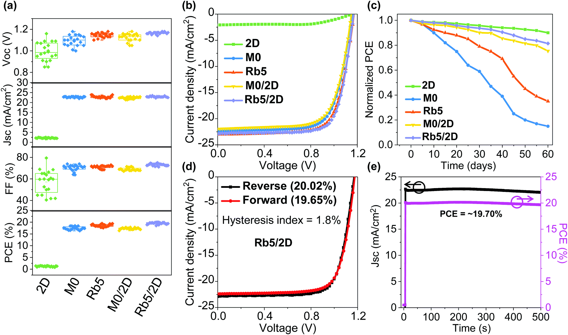 | ||
| Fig. 6 Solar cell characterization. (a) Statistics of 20–25 devices for 2D layered PEA2PbI4, 3D M0 and Rb5, and 3D/2D heterostructure perovskite solar cells. (b) J–V curves of the peak efficiency for each type of perovskite film. (c) Recorded long-term environmental stability of corresponding perovskite solar cells exposed to an ambient environment with 50% relative humidity without encapsulation. (d) J–V curve for the peak efficiency of 20.02% in the reverse scan (19.65% in the forward scan) obtained in the Rb5/2D perovskite solar cell. (e) The stabilized power output JSC and PCE are monitored versus time. | ||
Moreover, the statistical distribution of the PCEs of the 3D/2D perovskite solar cells using different concentrations of PEAI solution (1, 5, and 10 mg mL−1 in isopropanol) as 2D perovskite capping layers is also shown in Fig. S4b (ESI†). Average PCEs of 19.15 ± 0.55% and 19.5 ± 0.43% were obtained for the 1 and 5 mg mL−1 cases, respectively, higher than the average PCE (15.48 ± 0.62%) of the 10 mg mL−1 case. The deteriorated performance in the thicker 2D perovskite film may be attributed to the reduced charge transport property that originated from the severe quantum confinement effect.29 Decent charge carrier mobility can be obtained in the 3D/2D perovskite stacked structure (Fig. 5) when the thin 2D perovskite capping layer is controlled within the effective diffusion length.
Finally, the environmental stability of the perovskite solar cells was also evaluated. Unencapsulated devices were exposed to an ambient environment with ≈50% relative humidity in the dark at room temperature. The normalized PCEs versus time were recorded periodically (Fig. 6c). The devices incorporating small amounts of Rb+ cations and 2D layered perovskites exhibit significantly improved environmental stability. For example, the PCE retains 90%, 15%, 35%, 75%, and 81% of its initial value for 2D layered PEA2PbI4, 3D M0 and Rb5, and 3D/2D heterostructure (i.e., M0/2D and Rb5/2D) perovskite solar cells after 60 days of ambient exposure (50 ± 10% RH conditions without encapsulation). The far superior ambient stability of the 3D/2D heterostructure devices is partially attributed to fewer phase impurities present in the films43 and better phase stability since the addition of Rb+ and the hydrophobic 2D layered perovskites help to form an entropically stabilized phase and prevent direct contact of moisture. In addition, the environmental stability of the 3D/2D perovskite solar cells using different concentrations of PEAI solution (1, 5, and 10 mg mL−1 in isopropanol) as 2D perovskite capping layers was also evaluated (Fig. S4c, ESI†). The hysteresis index is determined using the equation:24 and reverse or forward represents the scan direction. Indeed, the hysteresis is also significantly improved within the Rb5/2D device partially due to suppressed trap formation, with a hysteresis index of 1.8% (Fig. 6d). We further demonstrated promising light-soaking stability of the cell at a fixed maximum power point voltage for 500 s, with a stabilized PCE of ≈19.70% under continuous illumination (Fig. 6e). This lasting illumination stability is due to suppressed phase conversion from the perovskite phase to non-perovskite phases, mainly assisted by the addition of Rb+ and Br− ions and 2D perovskite capping layer.37,44
Conclusions
In summary, we demonstrated that fine-tuning of a 2D layered perovskite as a capping layer on top of a classic 3D Rb+-doped perovskite could effectively alter the band structure and exhibit a more hydrophobic surface, leading to a significant improvement in device stability while maintaining good performance. The properties of the 2D capping layer and 3D Rb+-doped perovskite are put in context by comparison with 2D, 3D, and 3D/2D bilayer perovskites where we have investigated the electronic structure, composition, and carrier dynamics of these structures. The doping of Rb+ cations decreases the WF, and the addition of a 2D layered perovskite in 3D/2D bi-layer structures further decreases the WF compared to the classic 3D perovskites. The XPS depth profile shows that halides can migrate from the 3D into the 2D layer and a small amount of alkali metal can help to reduce the halide migration in both 3D and 3D/2D hybrid films. Through TRTS results, the average DC carrier mobility for the 3D/2D hierarchical structure and 3D perovskites is one order higher than the 2D PEA2PbI4 film, which is consistent with literature values, but providing only a minor distinction between the 3D/2D and 3D films. As a result, the optimal 3D/2D devices (i.e., Rb5/2D) incorporating the 2D layered perovskite and Rb+ alkali metal cations exhibit a significantly increased PCE over 20% in planar n–i–p devices, as well as improved stability at ≈50% relative humidity at room temperature without encapsulation. This work provides the perovskite community with a facile strategy and fundamental understanding to rationally design a 3D/2D bi-layer architecture with significant guidelines toward high-performance perovskite photovoltaics with improved operational stability.Author contributions
M.-C. T. and S. Z. contributed equally to this work. M.-C. T. designed and performed most of the experiments. M.-C. T. conducted device fabrication and measurements of optoelectronic properties and SEM analysis. C. A. H. and T. D. A. supervised the work. S. Z. and C. A. H. performed the UPS and XPS measurements. N. V. N. measured and simulated the ellipsometry spectra. T. M. and E. J. H. performed the time-resolved terahertz spectroscopy measurements. All authors provided critical feedback and helped with the research, analysis, and manuscript.Conflicts of interest
There are no conflicts to declare.Acknowledgements
Dr Tang acknowledges support under the Cooperative Research Agreement between the University of Maryland and the National Institute of Standards and Technology (NIST) with Federal Award 70NANB14H209. This work was supported by the King Abdullah University of Science and Technology (KAUST). All the commercial instruments and materials mentioned here are identified to foster understanding. Such identification does not imply recommendation or endorsement by the National Institute of Standards and Technology, nor does it imply that the materials or equipment identified are necessarily the best available for the purpose.References
- Q. Lin, A. Armin, R. C. R. Nagiri, P. L. Burn and P. Meredith, Nat. Photonics, 2015, 9, 106–112 CrossRef CAS
.
- A. Miyata, A. Mitioglu, P. Plochocka, O. Portugall, J. T.-W. Wang, S. D. Stranks, H. J. Snaith and R. J. Nicholas, Nat. Phys., 2015, 11, 582–587 Search PubMed
- F. Hao, C. C. Stoumpos, R. P. Chang and M. G. Kanatzidis, J. Am. Chem. Soc., 2014, 136, 8094–8099 CrossRef CAS
- A. K. Jena, A. Kulkarni and T. Miyasaka, Chem. Rev., 2019, 119, 3036–3103 CrossRef CAS
- S. Lee, M.-C. Tang, R. Munir, D. Barrit, Y.-J. Kim, R. Kang, J.-M. Yun, D.-M. Smilgies, A. Amassian and D.-Y. Kim, J. Mater. Chem. A, 2020, 8, 7695–7703 RSC
- Y. Fan, J. Fang, X. Chang, M.-C. Tang, D. Barrit, Z. Xu, Z. Jiang, J. Wen, H. Zhao, T. Niu, D.-M. Smilgies, S. Jin, Z. Liu, E. Q. Li, A. Amassian, S. Liu and K. Zhao, Joule, 2019, 3, 2485–2502 CrossRef CAS
- J. A. Christians, P. Schulz, J. S. Tinkham, T. H. Schloemer, S. P. Harvey, B. J. Tremolet de Villers, A. Sellinger, J. J. Berry and J. M. Luther, Nat. Energy, 2018, 3, 68–74 CrossRef CAS
- D. Barrit, Y. L. Zhang, T. H. Yang, M. C. Tang, R. P. Li, D. M. Smilgies, S. Z. Liu, T. D. Anthopoulos, A. Amassian and K. Zhao, Sol. RRL, 2020, 2000668 CrossRef
- J. M. Ball and A. Petrozza, Nat. Energy, 2016, 1, 1–13 Search PubMed
- Y. Hu, E. M. Hutter, P. Rieder, I. Grill, J. Hanisch, M. F. Aygüler, A. G. Hufnagel, M. Handloser, T. Bein, A. Hartschuh, K. Tvingstedt, V. Dyakonov, A. Baumann, T. J. Savenije, M. L. Petrus and P. Docampo, Adv. Energy Mater., 2018, 8, 1703057 CrossRef
- D. Barrit, P. Cheng, K. Darabi, M. C. Tang, D. M. Smilgies, S. Liu, T. D. Anthopoulos, K. Zhao and A. Amassian, Adv. Funct. Mater., 2020, 1907442 CrossRef CAS
- D. Barrit, P. Cheng, M.-C. Tang, K. Wang, H. Dang, D.-M. Smilgies, S. Liu, T. D. Anthopoulos, K. Zhao and A. Amassian, Adv. Funct. Mater., 2019, 29, 1807544 CrossRef CAS
- Y. Zhong, R. Munir, A. H. Balawi, A. D. Sheikh, L. Yu, M.-C. Tang, H. Hu, F. Laquai and A. Amassian, ACS Energy Lett., 2016, 1, 1049–1056 CrossRef CAS
- N. R. E. Laboratory, Best Research-Cell Efficiencies Chart, https://www.nrel.gov/pv/assets/pdfs/best-research-cell-efficiencies-190416.pdf, accessed 05 May, 2019.
- C. C. Boyd, R. Cheacharoen, T. Leijtens and M. D. McGehee, Chem. Rev., 2019, 119, 3418–3451 CrossRef CAS
- R. Wang, M. Mujahid, Y. Duan, Z.-K. Wang, J. Xue and Y. Yang, Adv. Funct. Mater., 2019, 29, 1808843 CrossRef CAS
- M.-C. Tang, Y. Fan, D. Barrit, R. Li, H. X. Dang, S. Zhang, T. J. Magnanelli, N. V. Nguyen, E. J. Heilweil, C. A. Hacker, D.-M. Smilgies, K. Zhao, A. Amassian and T. D. Anthopoulos, Sol. RRL, 2020, 2000272 CrossRef CAS
- Y. Liao, H. Liu, W. Zhou, D. Yang, Y. Shang, Z. Shi, B. Li, X. Jiang, L. Zhang, L. N. Quan, R. Quintero-Bermudez, B. R. Sutherland, Q. Mi, E. H. Sargent and Z. Ning, J. Am. Chem. Soc., 2017, 139, 6693–6699 CrossRef CAS
- T. Niu, J. Lu, X. Jia, Z. Xu, M. C. Tang, D. Barrit, N. Yuan, J. Ding, X. Zhang, Y. Fan, T. Luo, Y. Zhang, D. M. Smilgies, Z. Liu, A. Amassian, S. Jin, K. Zhao and S. F. Liu, Nano Lett., 2019, 19(10), 7181–7190 CrossRef CAS
- Y. Zhang, P. Wang, M.-C. Tang, D. Barrit, W. Ke, J. Liu, T. Luo, Y. Liu, T. Niu, D.-M. Smilgies, Z. Yang, Z. Liu, S. Jin, M. G. Kanatzidis, A. Amassian, S. F. Liu and K. Zhao, J. Am. Chem. Soc., 2019, 141, 2684–2694 CrossRef CAS
- V. Gonzalez-Pedro, E. J. Juarez-Perez, W. S. Arsyad, E. M. Barea, F. Fabregat-Santiago, I. Mora-Sero and J. Bisquert, Nano Lett., 2014, 14, 888–893 CrossRef CAS
- M. C. Tang, D. Barrit, R. Munir, R. P. Li, J. M. Barbe, D. M. Smilgies, S. Del Gobbo, T. D. Anthopoulos and A. Amassian, Sol. RRL, 2019, 3, 1800305 CrossRef
- Y. Zhong, R. Munir, J. Li, M.-C. Tang, M. R. Niazi, D.-M. Smilgies, K. Zhao and A. Amassian, ACS Energy Lett., 2018, 3, 1078–1085 CrossRef CAS
- T. Niu, J. Lu, M.-C. Tang, D. Barrit, D.-M. Smilgies, Z. Yang, J. Li, Y. Fan, T. Luo, I. McCulloch, A. Amassian, S. Liu and K. Zhao, Energy Environ. Sci., 2018, 11, 3358–3366 RSC
- Y. Hu, J. Schlipf, M. Wussler, M. L. Petrus, W. Jaegermann, T. Bein, P. Müller-Buschbaum and P. Docampo, ACS Nano, 2016, 10, 5999–6007 CrossRef CAS
- K. T. Cho, G. Grancini, Y. Lee, E. Oveisi, J. Ryu, O. Almora, M. Tschumi, P. A. Schouwink, G. Seo, S. Heo, J. Park, J. Jang, S. Paek, G. Garcia-Belmonte and M. K. Nazeeruddin, Energy Environ. Sci., 2018, 11, 952–959 RSC
- T. Ye, A. Bruno, G. Han, T. M. Koh, J. Li, N. F. Jamaludin, C. Soci, S. G. Mhaisalkar and W. L. Leong, Adv. Funct. Mater., 2018, 28, 1801654 CrossRef
- K. Wang, M. C. Tang, H. X. Dang, R. Munir, D. Barrit, M. De Bastiani, E. Aydin, D. M. Smilgies, S. De Wolf and A. Amassian, Adv. Mater., 2019, 31, e1808357 CrossRef
- P. Chen, Y. Bai, S. Wang, M. Lyu, J.-H. Yun and L. Wang, Adv. Funct. Mater., 2018, 28, 1706923 CrossRef
- Y. Lin, Y. Bai, Y. Fang, Z. Chen, S. Yang, X. Zheng, S. Tang, Y. Liu, J. Zhao and J. Huang, J. Phys. Chem. Lett., 2018, 9, 654–658 CrossRef CAS
- Z. Wang, Q. Lin, F. P. Chmiel, N. Sakai, L. M. Herz and H. J. Snaith, Nat. Energy, 2017, 2, 17135 CrossRef CAS
- F. Zhang, D. H. Kim, H. Lu, J.-S. Park, B. W. Larson, J. Hu, L. Gao, C. Xiao, O. G. Reid, X. Chen, Q. Zhao, P. F. Ndione, J. J. Berry, W. You, A. Walsh, M. C. Beard and K. Zhu, J. Am. Chem. Soc., 2019, 141, 5972–5979 CrossRef CAS
- A. H. Proppe, M. Wei, B. Chen, R. Quintero-Bermudez, S. O. Kelley and E. H. Sargent, J. Am. Chem. Soc., 2019, 141, 14180–14189 CrossRef CAS
- T. Zhou, H. Lai, T. Liu, D. Lu, X. Wan, X. Zhang, Y. Liu and Y. J. A. M. Chen, Adv. Mater., 2019, 31, 1901242 CrossRef
- Y. Bai, S. Xiao, C. Hu, T. Zhang, X. Meng, H. Lin, Y. Yang and S. J. A. E. M. Yang, Adv. Energy Mater., 2017, 7, 1701038 CrossRef
- L. Zhou, Z. Lin, Z. Ning, T. Li, X. Guo, J. Ma, J. Su, C. Zhang, J. Zhang, S. Liu, J. Chang and Y. Hao, Sol. RRL, 2019, 3, 1900293 CrossRef CAS
- S. Zhang, M.-C. Tang, Y. Fan, R. Li, N. V. Nguyen, K. Zhao, T. D. Anthopoulos and C. A. Hacker, ACS Appl. Mater. Interfaces, 2020, 12(30), 34402–34412 CrossRef CAS
- R. Ulbricht, E. Hendry, J. Shan, T. F. Heinz and M. Bonn, Rev. Mod. Phys., 2011, 83, 543–586 CrossRef CAS
- A. M. A. Leguy, Y. Hu, M. Campoy-Quiles, M. I. Alonso, O. J. Weber, P. Azarhoosh, M. van Schilfgaarde, M. T. Weller, T. Bein, J. Nelson, P. Docampo and P. R. F. Barnes, Chem. Mater., 2015, 27, 3397–3407 CrossRef CAS
- D. Zhao, H. Hu, R. Haselsberger, R. A. Marcus, M.-E. Michel-Beyerle, Y. M. Lam, J.-X. Zhu, C. La-o-vorakiat, M. C. Beard and E. E. M. Chia, ACS Nano, 2019, 13, 8826–8835 CrossRef CAS
- L. M. Herz, ACS Energy Lett., 2017, 2, 1539–1548 CrossRef CAS
- M.-C. Tang, Y. Fan, D. Barrit, X. Chang, H. X. Dang, R. Li, K. Wang, D.-M. Smilgies, S. Liu, S. De Wolf, T. D. Anthopoulos, K. Zhao and A. Amassian, J. Mater. Chem. A, 2020, 8, 1095–1104 RSC
- M. Saliba, T. Matsui, J. Y. Seo, K. Domanski, J. P. Correa-Baena, M. K. Nazeeruddin, S. M. Zakeeruddin, W. Tress, A. Abate, A. Hagfeldt and M. Gratzel, Energy Environ. Sci., 2016, 9, 1989–1997 RSC
- H. X. Dang, K. Wang, M. Ghasemi, M.-C. Tang, M. De Bastiani, E. Aydin, E. Dauzon, D. Barrit, J. Peng, D.-M. Smilgies, S. De Wolf and A. Amassian, Joule, 2019, 3, 1746–1764 CrossRef CAS
Footnotes |
| † Electronic supplementary information (ESI) available. See DOI: 10.1039/d0ma00967a |
| ‡ M.-C. Tang and S. Zhang contributed equally to this work. |
| This journal is © The Royal Society of Chemistry 2021 |