
From insulator to oxide-ion conductor by a synergistic effect from defect chemistry and microstructure: acceptor-doped Bi-excess sodium bismuth titanate Na0.5Bi0.51TiO3.015†
Fan
Yang
 *a,
Julian S.
Dean
b,
Qiaodan
Hu
c,
Patrick
Wu
b,
Emilio
Pradal-Velázquez
b,
Linhao
Li
b and
Derek C.
Sinclair
*b
*a,
Julian S.
Dean
b,
Qiaodan
Hu
c,
Patrick
Wu
b,
Emilio
Pradal-Velázquez
b,
Linhao
Li
b and
Derek C.
Sinclair
*b
aInstitute of Fuel Cells, School of Mechanical Engineering, Shanghai Jiao Tong University, 200240, Shanghai, China. E-mail: fanyang_0123@sjtu.edu.cn
bDepartment of Materials Science and Engineering, University of Sheffield, S1 3JD, UK. E-mail: d.c.sinclair@sheffield.ac.uk
cSchool of Materials Science and Engineering, Shanghai Jiao Tong University, 200240, Shanghai, China
First published on 23rd November 2020
Abstract
The influence of Ti-site acceptor-doping (Mg2+, Zn2+, Sc3+, Ga3+ and Al3+) on the electrical conductivity and conduction mechanism of a nominally Bi-excess sodium bismuth titanate perovskite, Na0.5Bi0.51TiO3.015 (NB0.51T), is reported. Low levels of acceptor-type dopants can introduce appreciable levels of oxide-ion conductivity into NB0.51T, i.e., 0.5% Mg-doping for Ti4+ can enhance the bulk conductivity of NB0.51T by more than 3 orders of magnitude with the oxide-ion transport number going from <0.1 for NB0.51T to >0.9 at 600 °C. The intriguing electrical behaviour in acceptor-doped NB0.51T dielectrics is a synergistic effect based on the defect chemistry and ceramic microstructure in these materials. NB0.51T ceramics with extremely low levels of doping show an inhomogeneous microstructure with randomly distributed large grains embedded in a small grained matrix. This can be considered as a two-phase composite with large grains as a conductive phase and small grains as an insulating phase based on an empirical conductivity – grain size relationship. Variation in the fraction of the conductive, large grained phase with increasing doping levels agrees with the oxide-ion transport number. This electrical two-phase model is supported by finite element modelling. This study reveals the significance of ceramic microstructure on the electrical conduction behaviour of these materials and can provide a guideline for selecting suitable doping strategies to meet the electrical property requirements of NBT-based ceramics for different applications.
Introduction
Sodium bismuth titanate, Na0.5Bi0.5TiO3 (NBT), can present three types of electrical behaviour by varying the A-site Bi content: (1) type I, oxide-ion conduction occurs in nominally stoichiometric NBT (NB0.50T) and Bi-deficient NBT (i.e., Na0.5Bi0.49TiO2.985, NB0.49T), with high bulk conductivities and oxide-ion transport numbers close to unity, i.e. σb > 10−3 S cm−1 and tion > 0.9 at 600 °C;1 (2) type II, mixed ionic–electronic conduction is observed in NBT with high levels of Bi excess (i.e., Na0.5Bi0.52TiO3.03, NB0.52T), with intermediate magnitude of σb (∼10−5 S cm−1, 600 °C) and tion ∼ 0.5;2 (3) type III, electrically insulating behaviour exists in slightly Bi-excess NBT (i.e., Na0.5Bi0.51TiO3.015, NB0.51T), with very low σb and tion close to zero, i.e. σb ∼ 10−6 S cm−1 and tion = 0.07, 600 °C.1 The diverse and tunable electrical properties make NBT-based materials promising candidates for applications in many important energy devices. For example, as electrolyte/electrode materials in intermediate-temperature solid oxide fuel cells (IT-SOFCs) and as high-permittivity dielectrics for multilayer ceramic capacitors (MLCCs).The flexible electrical conduction behaviour is attributed to the high mobility of oxygen ions in the NBT lattice as the highly polarisable Bi3+ ions with their 6s2 lone-pair electrons and weak Bi–O bonds provide pathways with low diffusion barriers for oxygen ion migration.3 A small number of oxygen vacancies can introduce a significant level of oxide-ion conduction into NBT according to σ = c × q × μ, where c, q and μ represent the concentration, charge and mobility of oxygen ions, respectively. For example, 0.25–0.5% oxygen deficiency, corresponding to an oxygen vacancy concentration of 0.083–0.167%, in the nominally stoichiometric NB0.50T caused by “accidental” Bi2O3-loss during ceramic processing,4 results in high conductivity of ∼10−3 S cm−1 at 600 °C. Tuning the conductivity and conduction mechanism among types I, II and III can therefore be achieved by various defect mechanisms such as A-site nonstoichiometry, acceptor- and donor-doping to manipulate the concentration of oxygen vacancies in NBT. In general, using the oxide-ion conducting NB0.50T as a reference, defect mechanisms that introduce additional oxygen vacancies, i.e., Bi-deficiency and acceptor-doping, can enhance σb by increasing the charge carrier concentration; on the contrary, defect mechanisms that reduce the concentration of oxygen vacancies, i.e., B-site Nb (donor) doping, suppress the contribution of oxide-ion conduction to σb, and switch the electrical behaviour from type I to type II when oxygen vacancies are partially filled, and to type III when the oxygen vacancy concentration is minimal. A detailed review of the defect chemistry-electrical property relationships of NBT can be found elsewhere.5
Apart from the above-mentioned magnitudes of σb and tion, the three types of electrical behaviour of undoped and doped NBTs can also be identified by the following empirical, indirect criteria: (1) oxygen nonstoichiometry. As the presence of oxygen vacancies is the pre-requisite for the oxide-ion conduction, NBT with a nominal composition that is oxygen deficient is likely to be oxide-ion conducting (type I). On the contrary, NBT with a nominal oxygen-excess composition is likely to be insulating (type III) or mixed conducting (type II). Caution should be made regarding the nominally oxygen-stoichiometric NBTs, which can be type I (e.g., NB0.50T), type II (e.g., (NB0.50T)0.8(BiScO3)0.2 solid solution6) and type III (e.g., (NB0.50T)0.93(BiAlO3)0.07 solid solution7). (2) Dielectric loss-temperature profile (tan![[thin space (1/6-em)]](https://www.rsc.org/images/entities/char_2009.gif) δ − T, 1 MHz). Type I NBT exhibit a rapid increase in tanδ with increasing temperature from ∼0.02 at room temperature to >0.2 at ∼300–400 °C. In contrast, tanδ of type III NBT initially decreases with increasing temperature and retain very low values of ∼0.005 over a temperature range between 300–600 °C and then show a rapid increase at higher temperatures. Type II NBT have similar tanδ − T profiles as type III in the low temperature ranges (<300 °C) but with an onset temperature for the rapid increase of tanδ between 300–600 °C. (3) Activation energy, Ea, of the bulk conductivity. One of the characteristic features on the σb Arrhenius plot of type I NBT is a change in Ea from ∼0.85 eV below 300 °C to ∼0.45 eV above 300 °C, which may be related to the coexistence of the rhombohedral and tetragonal polymorphs of NBT,8 or a combination of dissociation of defect clusters and different conduction paths in the various polymorphs.9 Type III NBT usually have Ea ∼ 1.6 eV at 500–800 °C (Ea in the low temperature range is unknown as the conductivity is too low to be measured below 500 °C). Type II NBT usually display Ea between 1.0–1.6 eV at T > 500 °C. (4) Microstructure. At the same sintering temperature (i.e., 1150 °C), type I NBT ceramics usually show much larger grains (∼10–20 μm for NB0.50T) than type III NBT (<5 μm).1 Significant variations in average grain size of type I, II and III NBT ceramics are also reported for the (NB0.50T)1−x(BiAlO3)x solid solution7 and Nb-doped NB0.50T, (Na0.5Bi0.5Ti1−yNbyO3+0.5y),2 in which the average grain size decreases with decreasing tion. This is not surprising as grain growth during sintering is a diffusion-controlled process, and the diffusion coefficient is proportional to the ionic conductivity according to Nernst–Einstein equation.
δ − T, 1 MHz). Type I NBT exhibit a rapid increase in tanδ with increasing temperature from ∼0.02 at room temperature to >0.2 at ∼300–400 °C. In contrast, tanδ of type III NBT initially decreases with increasing temperature and retain very low values of ∼0.005 over a temperature range between 300–600 °C and then show a rapid increase at higher temperatures. Type II NBT have similar tanδ − T profiles as type III in the low temperature ranges (<300 °C) but with an onset temperature for the rapid increase of tanδ between 300–600 °C. (3) Activation energy, Ea, of the bulk conductivity. One of the characteristic features on the σb Arrhenius plot of type I NBT is a change in Ea from ∼0.85 eV below 300 °C to ∼0.45 eV above 300 °C, which may be related to the coexistence of the rhombohedral and tetragonal polymorphs of NBT,8 or a combination of dissociation of defect clusters and different conduction paths in the various polymorphs.9 Type III NBT usually have Ea ∼ 1.6 eV at 500–800 °C (Ea in the low temperature range is unknown as the conductivity is too low to be measured below 500 °C). Type II NBT usually display Ea between 1.0–1.6 eV at T > 500 °C. (4) Microstructure. At the same sintering temperature (i.e., 1150 °C), type I NBT ceramics usually show much larger grains (∼10–20 μm for NB0.50T) than type III NBT (<5 μm).1 Significant variations in average grain size of type I, II and III NBT ceramics are also reported for the (NB0.50T)1−x(BiAlO3)x solid solution7 and Nb-doped NB0.50T, (Na0.5Bi0.5Ti1−yNbyO3+0.5y),2 in which the average grain size decreases with decreasing tion. This is not surprising as grain growth during sintering is a diffusion-controlled process, and the diffusion coefficient is proportional to the ionic conductivity according to Nernst–Einstein equation.
Since the discovery of high levels of oxide-ion conduction in NBT in 2014, there has been substantial efforts to enhance the bulk conductivity by incorporating acceptor-type dopants into NB0.50T and NB0.49T (type I). For example, Li+, Na+, Ca2+, Sr2+ and Ba2+ are introduced to partially replace Bi3+ on the A-site;8,10–13 Mg2+, Zn2+, Al3+, Sc3+ and Ga3+ to partially replace Ti4+ on the B-site.1,10,14–18 Detailed discussions on the defect chemistry induced by these acceptor dopants can be found in ref. 5 and 12. In all these cases, the lower positive charge caused by the acceptor dopants is compensated (ionically) by creation of oxygen vacancies. With the above attempts, σb is enhanced by ∼1 order of magnitude compared to NB0.50T and – half an order of magnitude compared to NB0.49T due to an increase in the oxygen vacancy concentration. An optimised σb is achieved using either A-site Sr-doping or B-site Mg-doping in NB0.49T, with σb approaching 10−2 S cm−1 and tion > 0.95 at 600 °C. Such a conductivity maximum is consistent with the oxygen vacancy diffusivity limit model in a perovskite lattice as proposed by R. A. De Souza.19
Here we investigate the effect of acceptor-doping on the electrical properties of a Bi-excess NBT, NB0.51T (type III), based on the following considerations. (1) Acceptor-doping such as Mg2+ and Sc3+ on the Ti-site will give nominal chemical formulae of Na0.5Bi0.51Ti1−xMgxO3.015−x and Na0.5Bi0.51Ti1−yScyO3.015−0.5y, respectively. According to the previously mentioned empirical relationship between conductivity and oxygen nonstoichiometry, we would expect compositional ranges of 0 < x < 0.015 and 0 < y < 0.03 whereby the ceramics remain electrically insulating. This may facilitate fine tuning of the material properties by acceptor-doping without a significant increase in the dielectric loss/leaky current, which may be useful for its application as a dielectric and piezo/ferroelectric. (2) According to molecular dynamics (MD) and molecular static (MS) simulations,20 A-site Bi vacancies are detrimental to diffusion of oxygen ions. NB0.50T and NB0.49T both have Bi vacancies due to either Bi loss during ceramic processing or intentional design to have a nominal Bi deficiency. It is therefore a curiosity to explore whether higher oxide-ion conductivity can be achieved in NB0.51T, in which the A-site is nominally fully occupied, by acceptor doping on the Ti-site with appropriate levels of doping. (3) As NB0.50T and NB0.49T already have high oxide-ion conductivity, enhancement of conductivity by acceptor doping is quite limited. The bulk conductivities of these acceptor-doped NBT are all within a narrow range on the σb Arrhenius plot,10 which makes it difficult to compare the impact of different dopants. Acceptor-doping in NB0.51T may induce a significant change in σb by several orders of magnitude. It is therefore of interest to investigate the difference among various dopants to provide a criterion for dopant selection.
Based on the reasoning above, we select various acceptor-type ions, including divalent Mg2+ and Zn2+, trivalent Al3+, Sc3+ and Ga3+, to partially replace Ti on the B-site of NB0.51T. The electrical properties of these acceptor-doped NB0.51T ceramics are established by a combination of impedance spectroscopy and electromotive force transport number measurements. It is surprising to find that extremely low levels of acceptor dopants (i.e., <0.5% for divalent ions) can introduce significant levels of oxide ion conduction into NB0.51T and change the conduction mechanism from insulating to ionic-conducting based on tion (i.e., tion > 0.9 for 0.25% Mg-doped NB0.51T). In contrast to NB0.50T and NB0.49T, we demonstrate that acceptor-doping in NB0.51T is a synergistic effect based on a combination of defect chemistry and ceramic microstructure. NB0.51T ceramics with extremely low doping levels exhibit inhomogeneous microstructures with randomly distributed large grains embedded in a small grained matrix. They can be considered (electrically) as a two-phase composite with the large grains being a conductive phase and the small grains being an insulating phase based on an empirical conductivity – grain size relationship. Finite element modelling is used to support this two-phase model. The formation mechanism of this inhomogeneous grain structure is not known but we suggest it is linked to the lack of homogenisation on acceptor-doping at such low levels during solid state synthesis. This can result in large conductive grains that are acceptor-rich and smaller grains that are acceptor-deficient or undoped. Analytical SEM is unable to detect the small variations in the level of dopants required to induce this effect; however, the grain size variations and electrical conductivity of NBT are sensitive to small levels of compositional variation. This work reveals the significance of ceramic microstructure on the electrical properties of NBT-based materials and can provide guidelines for selecting appropriate doping strategies to meet the electrical property requirements for different applications.
Experimental
Acceptor-doped NB0.51T ceramics, with chemical formulae of Na0.5Bi0.51Ti1−xMxO3.015−x (M = Mg and Zn) and Na0.5Bi0.51Ti1−yNyO3.015−0.5y (N = Sc, Al and Ga) were prepared by a solid state reaction method using Na2CO3 (99.5%, Fisher Chemical, UK), Bi2O3 (99.9%, Acros Organics, USA), TiO2 (99.9%, Sigma Aldrich, UK), MgO (99.9%, Alfa Aesar, UK), ZnO (99.9%, Fluka, UK), Sc2O3 (99.99%, Stanford Materials, USA), Al2O3 (99.95%, Alfa Aesar, UK) and Ga2O3 (99.9%, Sigma Aldrich, UK) as starting materials. Prior to weighing, the raw powders were dried overnight at 300 °C for Na2CO3 and Bi2O3, 600 °C for ZnO and Ga2O3, and 900 °C for TiO2, MgO, Sc2O3 and Al2O3. Appropriate amounts of each precursor were weighed and ball-milled in iso-propanol using yttria-stabilised zirconia grinding media for 6 hours. The mixture was dried overnight in an 85 °C oven, sieved and then calcined at 800 °C for 2 hours. The resultant powders were subjected to a second round of ball milling, drying, sieving and calcination and subsequently to a final, third round of ball milling and sieving. The products were compacted into pellets by uni-axial cold pressing followed by isostatic pressing at 200 MPa. Pellets were embedded in sacrificial powder of the same composition and sintered at 1150 °C for 2 hours. After sintering, pellets were removed from the sacrificial powder and ground using SiC sand papers to obtain flat surfaces.Phase purity was examined by X-ray diffraction on the pellet surface using a Bruker D2 phaser or on crushed pellets using a high-resolution STOE STADI-P diffractometer. Ceramic microstructures were observed by scanning electron microscopy (SEM, JEOL JSM-6010LA, JEOL Ltd., Tokyo, Japan) on thermally etched surfaces. The grain size distribution of each ceramic was measured from the SEM images using ImageJ software. Compositions were analysed by energy-dispersive X-ray spectroscopy (EDS) on 5–10 randomly selected areas on the carbon-coated polished surfaces (without thermal etch).
Electrical properties were measured by impedance spectroscopy using an Agilent E4980A impedance analyser (Agilent Technologies Inc., Palo-Alto, CA; frequency range 1 MHz to 20 Hz) or a Solartron 1260 system (Solartron Analytical, UK; frequency range 1 MHz to 20 Hz) using Au paste (fired at 850 °C for 2 h) as electrodes. All impedance data were corrected for high frequency inductance associated with the leads and the measurement jig by performing a short circuit measurement and normalised by a geometric factor (thickness/surface area). Equivalent circuit fitting was performed using ZView software (Scribner Associates, Inc, Southern Pines, NC). Dielectric properties were measured using an LCR meter (Agilent E4980 Precision LCR Meter, Agilent Technologies) with an applied ac voltage of 100 mV. Data points were collected every 60 s from room temperature (RT) to 800 °C using a non-inductively wound tube furnace at a ramp rate of 1 °C min−1. Oxygen-ion transport number measurements were performed using a ProboStat™ system (NorECs Norwegian Electro Ceramics AS, Oslo, Norway). Details of the measurement can be found in previous publications.1,7
To study how materials properties (conductivity and permittivity) and a collection of non-uniform grains influence the electrical response we use an in-house developed FEM package, ElCer, to simulate the electrical response of electro-ceramics.21 The models are first constructed using 3D Voronoi tessellation. Each volume, representing a grain, is then meshed and assigned its own conductivity and permittivity value. ElCer is then used to solve the complete electrical response of the system through Maxwell's equations and the response converted into an impedance spectrum that can be analysed and compared to experimental results.
Results
Phase, microstructure, and composition
Na0.5Bi0.51Ti1−xMgxO3.015−x (x = 0, 0.001, 0.0025, 0.005, 0.01, 0.015 and 0.02) ceramics are phase-pure based on laboratory XRD (Fig. 1a). An expanded view of the 2θ range between 37 and 42° shows the superlattice reflection of a rhombohedral structure for all compositions (Fig. 1b). XRD patterns for other acceptor-doped NB0.51T are given in ESI (Fig. S1–S3† for Sc, Al and Ga-doping, respectively).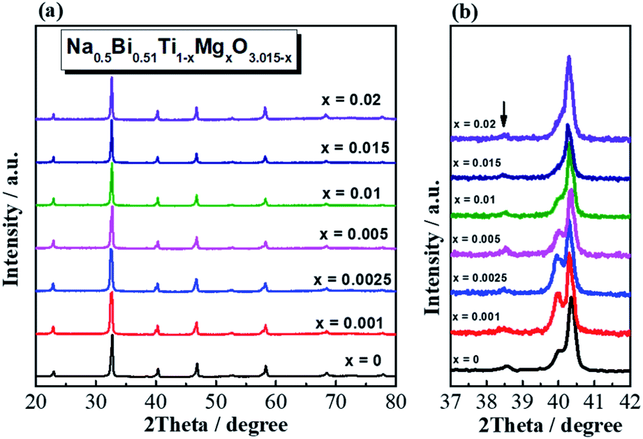 | ||
| Fig. 1 (a) Room temperature XRD patterns of Na0.5Bi0.51Ti1−xMgxO3.015−x (x = 0, 0.001, 0.0025, 0.005, 0.01, 0.015 and 0.02) ceramics and (b) an expanded view of the 2θ range between 37 and 42° showing the superlattice reflection of the rhombohedral structure as indicated by the arrow. | ||
SEM images of thermally-etched surfaces of Na0.5Bi0.51Ti1−xMgxO3.015−x ceramics with selected compositions are presented in Fig. 2, where apparent grain growth can be observed with increasing x. Undoped NB0.51T ceramics have uniform, small grains with an average grain size of ∼1–2 μm (Fig. S4†). With extremely low levels of Mg-doping (i.e., x = 0.001, Fig. 2a), ceramics show an inhomogeneous microstructure with a small number of large grains (∼5–10 μm) randomly distributed in a small grained (∼2 μm) matrix. With increasing x, i.e., x = 0.0025 and 0.005, the inhomogeneous grain structure still exists albeit the number of large grains, as well as the grain sizes, increase (Fig. 2b–d). Detailed analyses of the grain size distribution are given in Fig. S5.† Inhomogeneous distribution of large grains embedded in small grains when the doping level is extremely low is also observed in NB0.51T ceramics doped with Zn, Sc, Al and Ga. Typical SEM images are shown in Fig. S6 (for Zn) and S7 (for Sc).†
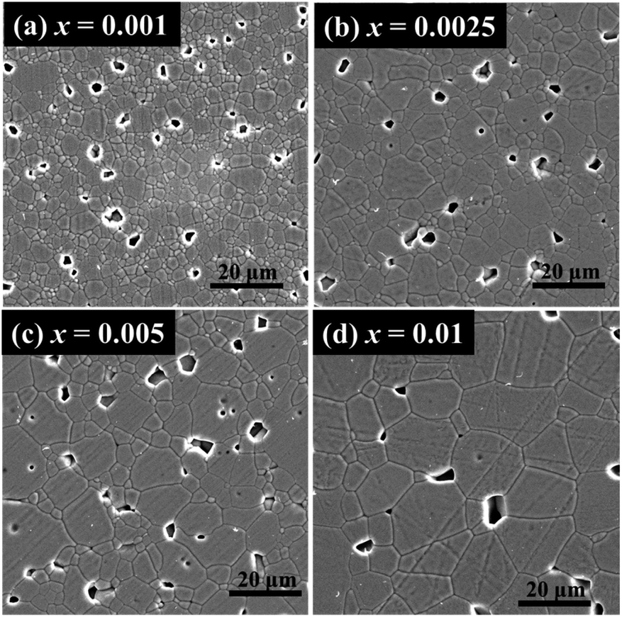 | ||
| Fig. 2 SEM micrographs of thermally-etched surfaces of Na0.5Bi0.51Ti1−xMgxO3.015−x ceramics. (a) x = 0.001; (b) x = 0.0025; (c) x = 0.005; (d) x = 0.01. | ||
Chemical compositions of Na0.5Bi0.51Ti1−xMgxO3.015−x ceramics analysed by EDS on polished surfaces (without thermal-etching) are listed in Table 1. The cation ratios are normalised to 100% for ease of comparison. For this series, the nominal atomic percentages of Na and Bi are fixed at 24.88 and 25.37%, respectively, whereas those of Ti and Mg vary with increasing x. The measured values generally agree with the nominal values; however, the measured values are associated with large errors, indicating the elemental distribution, in particular, Mg, in the ceramics is inhomogeneous. It is noteworthy that the Kα line for Mg (1.25 keV) is close to that for Na (1.04 keV),1 therefore, accurate acquisition of the atomic percentages of these cations is challenging. Nevertheless, the variation of atomic percentages of Ti and Mg with increasing x does provide qualified evidence that Mg is incorporated into NB0.51T. EDS analysis on a thermally-etched Zn-doped NB0.51T (x = 0.005) is given in Table S1,† where an inhomogeneous elemental distribution of the dopant is also observed.
| x | Na | Bi | Ti | Mg | ||
|---|---|---|---|---|---|---|
| Nominal | EDS | Nominal | EDS | |||
| 0 | 24.71 ± 0.40 | 25.43 ± 0.36 | 49.75 | 49.85 ± 0.41 | 0 | NA |
| 0.001 | 23.95 ± 1.21 | 26.26 ± 0.47 | 49.70 | 49.76 ± 0.93 | 0.05 | 0.15 ± 0.23 |
| 0.0025 | 23.97 ± 1.14 | 26.60 ± 0.43 | 49.63 | 49.49 ± 0.60 | 0.12 | 0.17 ± 0.21 |
| 0.005 | 23.36 ± 0.55 | 26.80 ± 0.31 | 49.50 | 49.35 ± 0.32 | 0.25 | 0.51 ± 0.51 |
| 0.01 | 23.65 ± 0.68 | 26.98 ± 0.30 | 49.25 | 48.66 ± 0.57 | 0.50 | 0.71 ± 0.46 |
| 0.015 | 24.16 ± 0.96 | 26.68 ± 0.67 | 49.00 | 48.18 ± 0.64 | 0.75 | 0.99 ± 0.41 |
| 0.02 | 24.46 ± 0.77 | 26.35 ± 0.71 | 48.76 | 48.06 ± 0.81 | 1.00 | 1.23 ± 0.59 |
Electrical properties
Complex impedance plane (Z*) plots and M′′ − logf spectroscopic plots measured at 600 °C in flowing nitrogen, air and oxygen for selected compositions are shown in Fig. 3. The Z* plot for undoped NB0.51T, Fig. 3a, shows a single arc. The associated capacitance of the arc is ∼8 × 10⁻¹¹ F cm−1, corresponding to a relative permittivity (εr) of ∼900, which agrees with the value for paraelectric NBT at this temperature. The single arc in the Z* plot for NB0.51T therefore represents the bulk response, which is smallest in nitrogen and largest in oxygen, suggesting n-type electronic behaviour. This is in agreement with previous studies.1 The corresponding M′′ − logf spectroscopic plots of undoped NB0.51T, Fig. 3b, show a single Debye peak with a characteristic frequency, fmax, of 5.01 kHz in air and oxygen and 3.98 kHz in nitrogen. For x = 0.001, the Z* plot (Fig. 3c) shows a distorted arc with an obvious low-frequency spike (indicated in the highlighted oval). The arc is smallest in nitrogen, suggesting the presence of n-type electronic conduction; the electrode spike is most prominent in nitrogen and least prominent in oxygen, suggesting the presence of oxide-ion conduction. NB0.51T with 0.1% Mg-doping (x = 0.001) therefore shows mixed electronic–ionic conduction behaviour. The corresponding M′′ − logf spectroscopic plots for this composition, Fig. 3d, show a broad peak with fmax = 12.5 kHz. The broad M′′ peak is an indication of either chemical or microstructural inhomogeneity, which agrees with the information from SEM (Fig. 2a) and Table 1. With increasing doping level, for example x = 0.005, Z* plots (Fig. 3e) show two arcs with a large low frequency spike. The high frequency arc, corresponding to the bulk, is not dependent on pO2, as shown by the inset figure. The associated capacitance for this high-frequency response is 1.33 × 10⁻¹⁰ F cm−1, corresponding to a permittivity value of ∼1400, which agrees with the permittivity of bulk NBT at 600 °C. The medium frequency arc is smallest in oxygen and largest in nitrogen, suggesting a predominant p-type electronic conduction mechanism. The associated capacitance is 1.37 × 10⁻⁹ F cm−1, one order of magnitude higher than that of the high-frequency response, may be attributed to either a grain boundary response or a less conductive bulk phase (discussed later). The low frequency electrode spike is largest in nitrogen and smallest in oxygen, indicating the presence of oxide-ion conduction. Combining the above information, the bulk conduction of x = 0.005 is dominated by oxygen ions. The corresponding M′′ − logf spectroscopic plot, Fig. 3f, shows a pO2-independent peak at fmax = 631 kHz. For x = 0.015, Z* plots, Fig. 3g, are dominated by a grain boundary response and the electrode effect. An expanded view of the high frequency range (inset of Fig. 3g) shows a pO2-independent intercept with the Z′-axis, corresponding to the resistance of the bulk, suggesting an oxide-ion conduction mechanism. The M′′ peak is beyond the highest measured frequency, therefore fmax exceeds 1 MHz, Fig. 3f. The above information from impedance spectroscopy indicates that, with very low levels of Mg doping, it is possible to change the electrical conduction mechanism of NB0.51T from n-type electronic (type III) to mixed electronic–ionic (type II) and finally to oxide-ion conduction (type I).
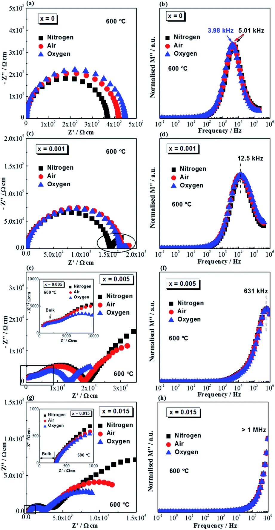 | ||
| Fig. 3 Impedance spectroscopy data of Na0.5Bi0.51Ti1−xMgxO3.015−x (x = 0, 0.001, 0.005 and 0.015) ceramics at 600 °C in flowing nitrogen, air and oxygen in the frequency range from 1 MHz to 0.1 Hz. (a), (c), (e) and (g): Z* plots for x = 0, 0.001, 0.005 and 0.015, respectively. Inset figures in (e) and (g) are an expanded view of the region in the rectangle. (b), (d), (f) and (h): M′′ − logf spectroscopic plots for x = 0, 0.001, 0.005 and 0.015, respectively. The numbers inside each figure indicate the frequency at the M′′ maxima. | ||
Arrhenius plots of bulk conductivity, σb = 1/Rb, for Na0.5Bi0.51Ti1−xMgxO3.015−x (x = 0, 0.001, 0.0025, 0.005, 0.01, 0.015 and 0.02) ceramics over a range of temperatures are shown in Fig. 4. Based on the magnitude of σb, these ceramics can be divided into three groups: (1) x = 0 and 0.001, σb values are very low (so they can be measured only at high temperatures). In the temperature range between 500 and 800 °C, σb − 1000T−1 shows a linear relationship with Ea values of 1.69 eV for x = 0 and 1.31 eV for x = 0.001; (2) x = 0.0025 and 0.005, show intermediate σb values. σb − 1000T−1 relationships show a change in Ea from ∼0.8 eV below 300 °C to ∼0.4 eV above 300 °C; (3) x ≥ 0.01, σb values are high, and also show a change in Ea at ∼300 °C. The change in Ea at ∼300 °C has been discussed in previous studies and is attributed to the coexistence of rhombohedral and tetragonal NBT polymorphs between 250 and 400 °C (ref. 8) or as a combination of defect associates and polymorphic phase transitions.9 As a change in Ea at ∼300 °C is a characteristic of type I NBT, the data in Fig. 4 suggests the bulk conduction of Na0.5Bi0.51Ti1−xMgxO3.015−x ceramics with x ≥ 0.0025 is predominantly by migration of oxygen ions. σb Arrhenius plots for other acceptor-doped NB0.51T show similar behaviour and are given in ESI, Fig. S8–S11.†
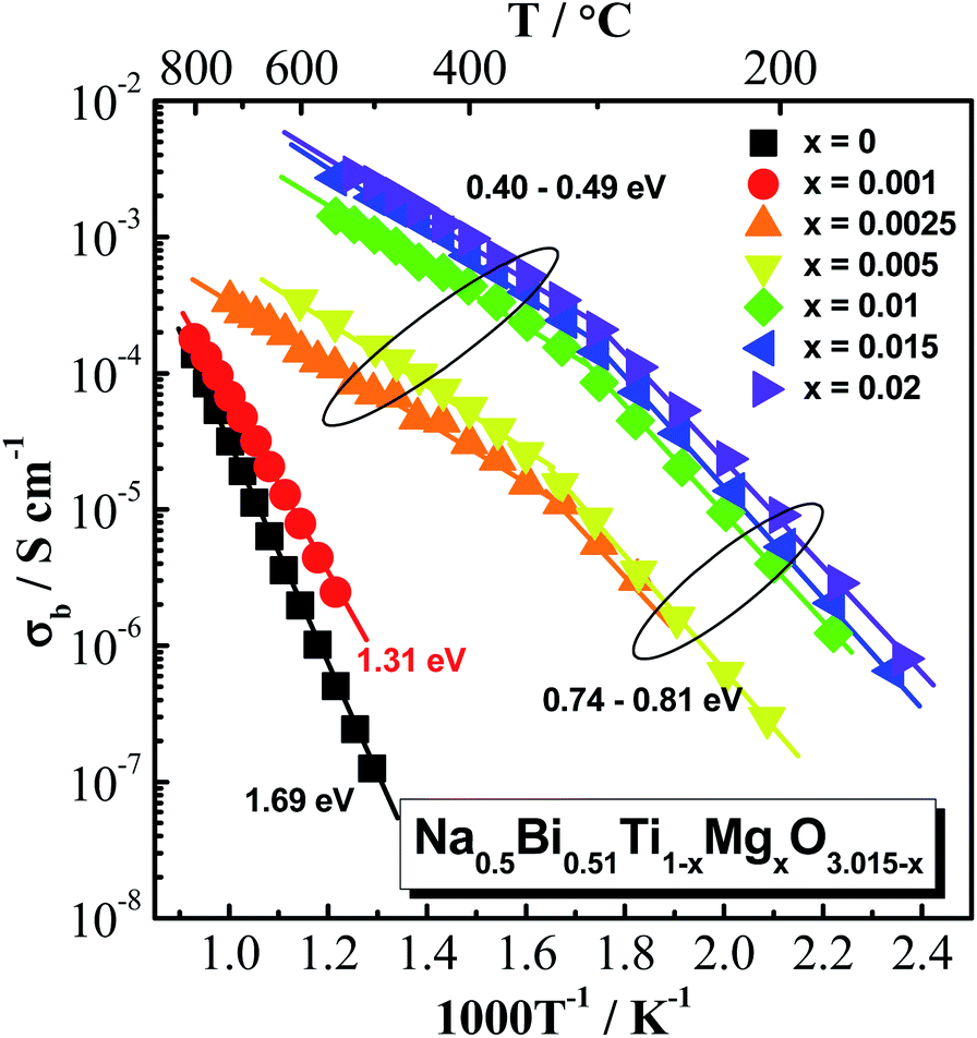 | ||
| Fig. 4 Arrhenius plot for bulk conductivity, σb, of Na0.5Bi0.51Ti1−xMgxO3.015−x (x = 0, 0.001, 0.0025, 0.005, 0.01, 0.015 and 0.02) ceramics measured in air. Numbers in eV are the activation energies associated with bulk conduction. | ||
Oxygen-ion transport number, tion, as a function of x is shown in Fig. 5. Undoped NB0.51T (x = 0) has tion close to zero, suggesting a predominant electronic conduction mechanism; x = 0.001 has tion ∼ 0.35, suggesting mixed electronic–ionic conduction behaviour; x ≥ 0.025 have tion > 0.9, suggesting predominant oxide-ion conduction behaviour. These tion values further confirm the information obtained from the pO2 dependence of σb and the σb − 1000T−1 relationship that very low levels of acceptor doping (i.e., 0.25 and 0.5%) can change the bulk conduction of NB0.51T from electronic to ionic, although the magnitude of σb is below 10−3 S cm−1 and resides in the type II region (Fig. 5).
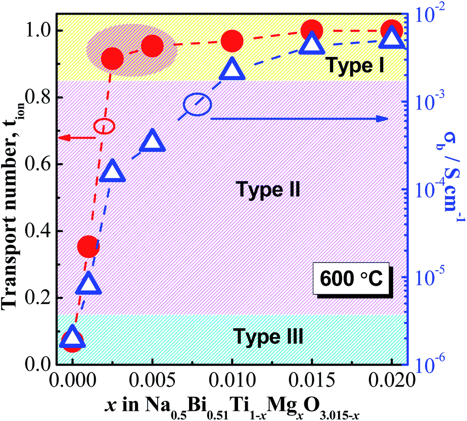 | ||
| Fig. 5 Oxygen-ion transport number, tion, and bulk conductivity, σb, at 600 °C versus x. | ||
Dielectric properties
Permittivity-temperature (εr − T, 1 MHz) and dielectric loss-temperature (tanδ − T, 1 MHz) profiles for Na0.5Bi0.51Ti1−xMgxO3.015−x (x = 0, 0.001, 0.0025, 0.005, 0.01, 0.015 and 0.02) ceramics are shown in Fig. 6. Incorporation of Mg2+ into NB0.51T does not change the permittivity maximum or the temperature of the permittivity maximum, Tm (Fig. 6a) but it has a significant effect on the tanδ − T profile (Fig. 6b). NB0.51T (x = 0) shows very low tanδ over a wide temperature range (<0.02 between 300 and 700 °C). x = 0.001, 0.0025 and 0.005 show low tanδ in a narrower temperature range and a steep rise between 350 and 700 °C. With high doping levels, i.e., x = 0.01, 0.015 and 0.02, tanδ shows a sharp rise with increasing temperature and it exceeds 0.2 at ∼350 °C. With increasing Mg doping level, the tanδ − T relationship of NB0.51T presents a shift from type III behaviour to type II and finally to type I. Similar dielectric behaviour is observed for other B-site acceptor-doped NB0.51T ceramics as shown in Fig. S12–S15.†
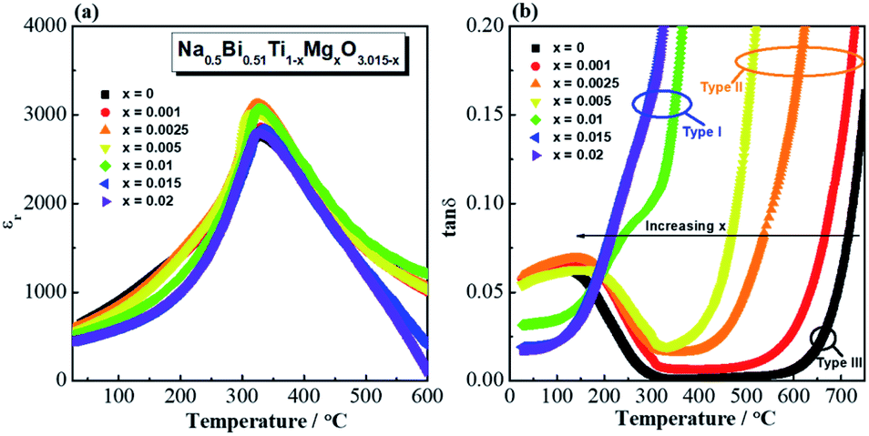 | ||
| Fig. 6 Dielectric spectroscopy for Na0.5Bi0.51Ti1−xMgxO3.015−x (x = 0, 0.001, 0.0025, 0.005, 0.01, 0.015 and 0.02) ceramics: (a) permittivity at 1 MHz versus temperature and (b) dielectric loss, tanδ, (1 MHz) versus temperature. | ||
Comparison of various dopants
σ b for NB0.51T with various acceptor dopants and doping levels measured at 500 °C in air are shown in Fig. 7. For all the acceptor-type dopants investigated in this work, very low levels of doping can significantly enhance σb of NB0.51T by more than three orders of magnitude. For the divalent ions, Fig. 7a, doping NB0.51T with Mg shows higher σb than that with Zn; for trivalent dopants, Fig. 7b, the highest σb in NB0.51T occurs with Sc doping, the lowest with Al and intermediate with Ga.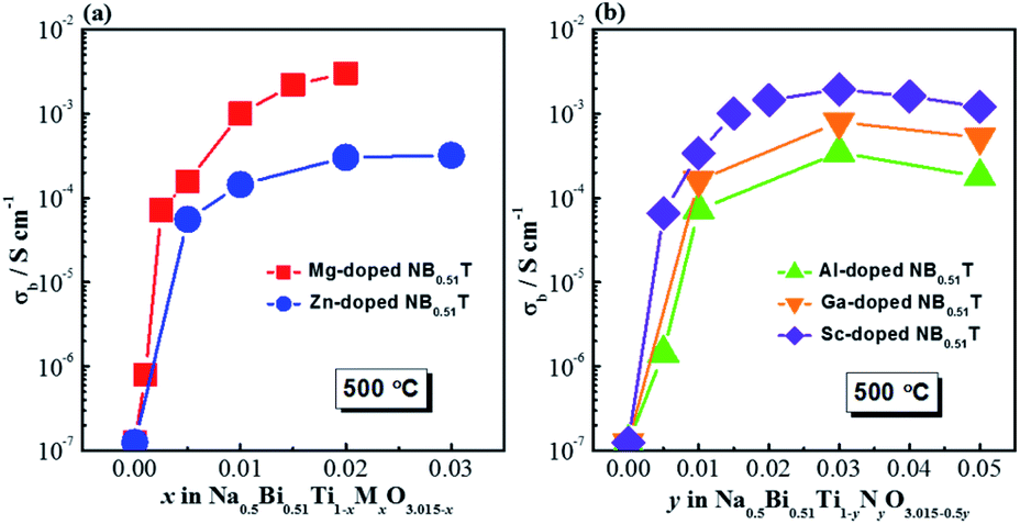 | ||
| Fig. 7 Bulk conductivity, σb, for Na0.5Bi0.51TiO3.015 with various acceptor dopants and doping levels: (a) divalent dopants Mg2+ and Zn2+; (b) trivalent dopants Al3+, Ga3+ and Sc3+. | ||
Discussion
Synergistic effect of defect chemistry and ceramic microstructure
Defect chemistry in B-site acceptor-doped NB0.51T, using Mg as an example, can be described by the following two defect equations,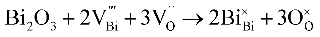 | (1) |
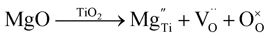 | (2) |
As the presence of oxygen vacancies is a pre-requisite for oxide-ion conduction, σb and tion of NBT-based materials usually exhibit a strong dependence on the nominal oxygen deficiency, δ, with an “onset” transition between low σb (<10−5 S cm−1) and tion (<0.1), to high σb (>10−3 S cm−1) and tion (>0.9) near δ = 0, as presented by the open circles in Fig. 8. If starting from a Bi-excess NBT, i.e., Na0.5Bi0.51TiO3.015, acceptor-doping such as Mg2+ on the Ti4+ site will give a chemical formula of Na0.5Bi0.51Ti1−xMgxO3.015−x. Based on the previous findings of the σb − δ and tion − δ relationship in Fig. 8, a transition from insulating to conducting at x = 0.015 may be expected; however, it is surprising to notice that extremely low levels of Mg2+ (i.e., x ≤ 0.005) can introduce considerable levels of oxide ion conduction into NB0.51T and change the conduction mechanism from insulating to ionic-conducting based on tion (i.e., tion > 0.9 for x = 0.0025), as shown by the solid red spheres in Fig. 8. The unexpected discovery that acceptor-doping in NB0.51T shifts the onset transition in oxygen deficiency to δ < 0 suggests an additional mechanism, other than the defect chemistry induced by acceptor doping, should be considered.
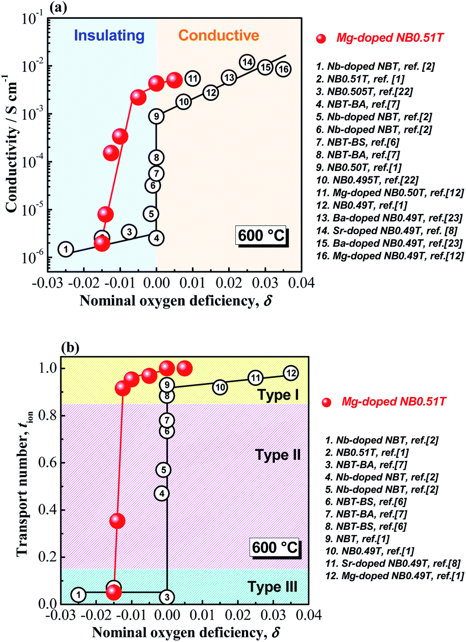 | ||
| Fig. 8 (a) Bulk conductivity, σb and (b) oxide-ion transport number, tion of NBT-based materials as a function of nominal oxygen deficiency, δ. The solid spheres represent the data for Mg-doped NB0.51T in this work, and the open circles are data from literature. | ||
An important microstructural feature of acceptor-doped NB0.51T with low doping levels is the inhomogeneous and random distribution of large grains in a small grained matrix, presumably based on a variation in the distribution of the low level of acceptor dopants via the solid-state reaction route used to prepare the ceramics. This motivated us to explore the possible impact from the ceramic microstructure on the conductivity of the ceramics. Conductivity values for NBT-based ceramics are summarised from literature and plotted as a function of average grain size in Fig. 9. There is a critical grain size of ∼3.5 μm, below which NBT ceramics have low conductivity and above which they have high conductivity.
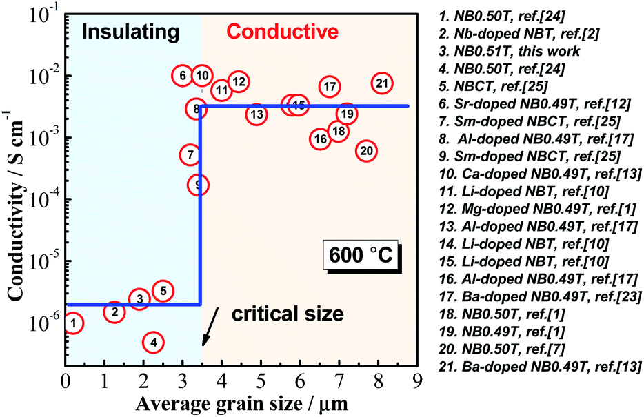 | ||
| Fig. 9 Conductivity-average grain size relationship of nonstoichiometric and doped NBT ceramics. | ||
Combining effect of oxygen deficiency, δ, and grain size, d, on conductivity is illustrated by the contour map in Fig. 10. In general, the high conductivity region (orange and red colours) lies in the top-right where δ has a large, positive value and d is large, and the low conductivity region (blue colour) lies in the bottom-left where δ is negative and d is small. This suggests that in most cases, conductivity of NBT-based materials is determined by oxygen deficiency; however, there are two unexpected regions, as marked by the dashed ellipses. Region (1): d > 3.5 μm, conductivity increases with increasing grain size even if δ < 0; region (2): d < 3.5 μm, conductivity remains low although δ > 0. This suggests that in these two regions, conductivity is determined by the grain size rather than oxygen deficiency. For Na0.5Bi0.51Ti1−xMgxO3.015−x investigated in this work, three compositions x = 0.0025, 0.005 and 0.01, are within region (1).
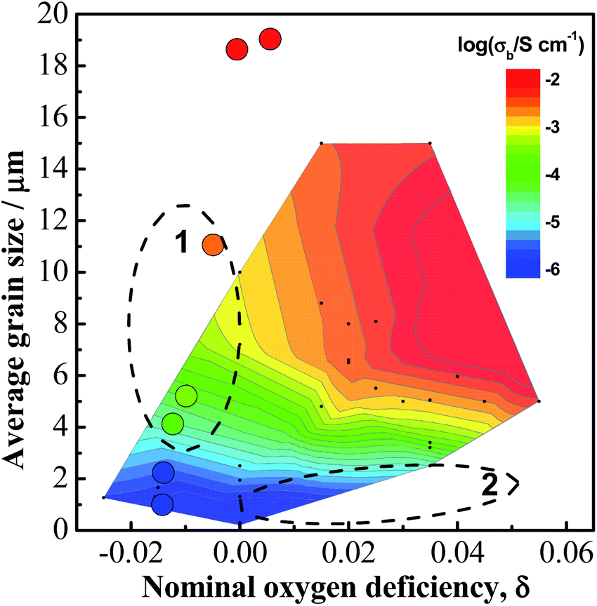 | ||
| Fig. 10 A contour map showing the dependence of bulk conductivity (at 600 °C) on nominal oxygen deficiency and average grain size. The contour map is plotted based on data collected from references listed in Fig. 8 and 9. The filled circles are experimental data from this work. | ||
As grain size has a large impact on the conductivity, we plot the statistical grain size distribution for each composition, as shown in Fig. S5.† With increasing x there is an increase in the average grain size, however there is also an increasingly broader grain size distribution. According to the conductivity-grain size relationship in Fig. 9, d = 3.5 μm is used as the critical grain size and the relative fraction of grains with d > 3.5 μm (defined as large grains) is calculated and presented in Fig. 11, where a rapid increase in the number fraction of large grains from 0 to ∼90% can be observed between x = 0–0.01. This fraction approaches 100% for x = 0.015 and 0.02. Although the fraction of large grains is calculated based on two-dimensional SEM images and thus may deviate from the three-dimensional volume fraction, it still shows a trend that the number of large grains increases with increasing x. Furthermore, the area fraction in 2D should be similar to the volume fraction in 3D in the case of randomly distributed large grains and a randomly selected area for observation according to the theory of quantitative stereology.26
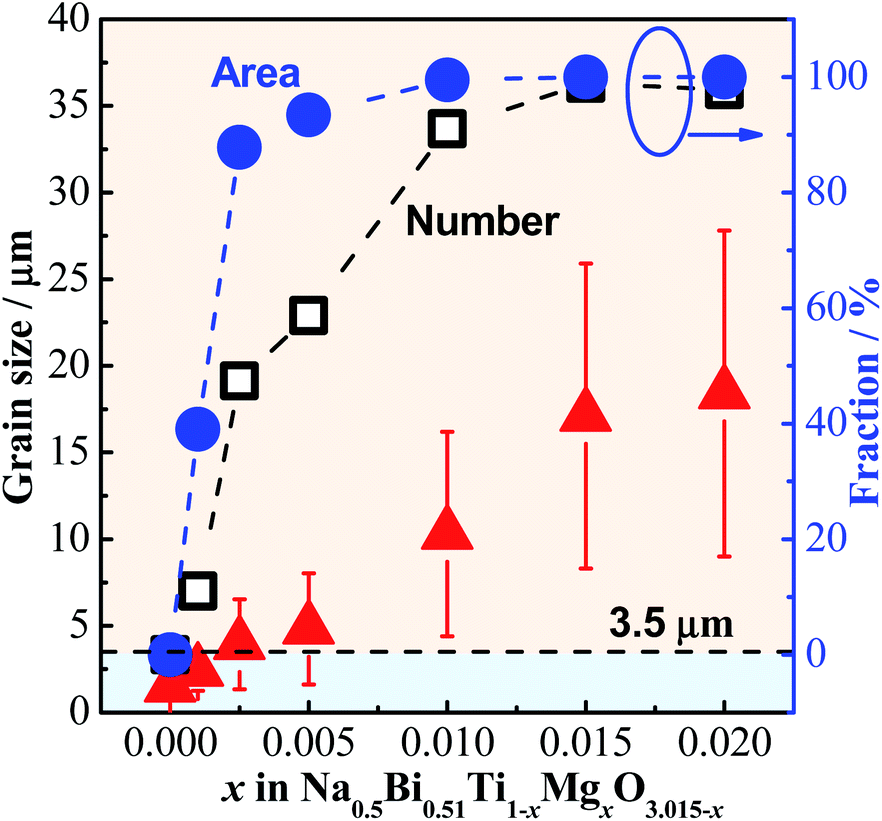 | ||
| Fig. 11 Average grain size (filled triangles), number (open squares) and area (filled cycles) fractions of large grains (d > 3.5 μm) as a function of x. The horizontal dash line represents the critical grain size for the insulating-conductive transition. | ||
Combining the information from Fig. 9–11, Na0.5Bi0.51Ti1−xMgxO3.015−x ceramics with low levels of Mg-doping (x = 0.001, 0.0025, 0.005 and 0.01) consist of two types of grains: d > 3.5 μm (large grains, high conductivity) and d < 3.5 μm (small grains, low conductivity). For impedance spectroscopy measurements, the electrical current is going to take the path of least resistance and thus favour the larger conductive grains and avoid the smaller, resistive grains. Impedance data are therefore dominated by the conductive phase (large grains) when percolation is achieved.
Electrical conductivity of a composite with a random distribution of two phases can usually be predicted by a percolation theory. When the volume fraction of the conductive phase reaches a certain threshold, typically ∼16%,27 the conductive phase can interconnect in the composite structure forming a conduction path that results in a dramatic increase in the effective conductivity of the sample. To further discuss the possible impact from the two-phase microstructure, finite element modelling (FEM) was employed to simulate conductivity data using ElCer.21
First a 3D geometric model is established for each value of x using a Voronoi tessellation process to create 512 grains. Adopting a standard Voronoi tessellation21 is insufficient to replicate this microstructure here, as the algorithm would divide up the space between the initial seed points equally. As such the models generated would produce a normal distribution of grain sizes, where the smaller grains would surround the larger one and grow in size as they near them. To overcome this, we use a feature in Voro++28 known as radical Voronoi tessellation. This has been used previously to successfully model the percolation effects in composite materials.29 Each discretized seed point is weighted with a value. These weights were then randomised, generating a special distribution of larger and smaller grains throughout the model. The distribution of grain areas is created such that the fraction of large grains (d > 3.5 μm) matches the values obtained from SEM as given by the blue filled symbols in Fig. 11. An example of one of these models is shown in Fig. 12a for x = 0.010. Three electrical models for each geometrical model were investigated based on a two-phase mixture where the materials properties of conductivity and permittivity were assigned as σ1 and ε1 for the insulating phase and σ2 and ε2 for the conductive phase. The area fraction of large grains (d > 3.5 μm) was assigned as the fraction of conductive grains (σ2). In all three models, ε1 and ε2 were fixed at a value of 1000 (for ε) and σ1 assigned 1.8 × 10⁻⁶ S cm−1. The magnitude of σ2 for each value of x was based on three scenarios of conductivity (explained below) but in each case had an upper limit of 4 × 10⁻³ S cm−1. The lower and upper limits of conductivity for the FEM analysis were based on the experimental results shown in Fig. 5 for x = 0 (1.8 × 10⁻⁶ S cm−1) and x = 0.015 (4 × 10⁻³ S cm−1), respectively.
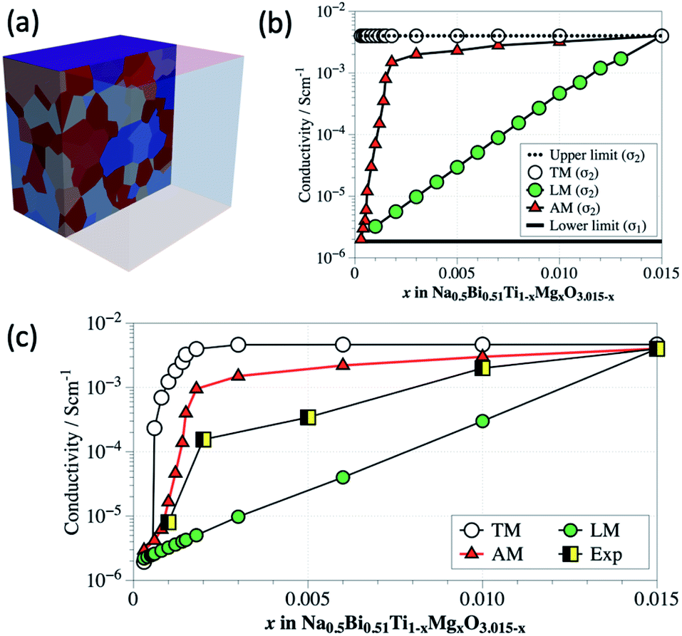 | ||
| Fig. 12 (a) A 3D geometric model for finite element simulations; (b) the relationship between Mg content, and the upper and lower conductivity limits. The lower limit is assigned to σ1, the upper limit is modified and assigned to σ2 through a TM (threshold model), LM (linear model) and AM (area model). (c) Calculated dc conductivity versus x using three separate conductivity profile models TM, LM and AM, in comparison with experimental results (Exp.). | ||
The first is a threshold model (TM). Any grain with diameter exceeding the threshold of 3.5 μm is assumed to be conducting and set as σ2 = 4 × 10⁻³ S cm−1 with all other grains assumed to be insulating and therefore set as σ1 = 1.8 × 10⁻⁶ S cm−1, as shown by the horizontal lines in Fig. 12b. The second is based a linear model (LM) where the grain conductivity (on a logarithmic scale) is a linear interpolation of the Mg content, x, ranging from σ1 = 1.8 × 10⁻⁶ S cm−1 for x = 0 to σ2 = 4 × 10⁻³ S cm−1 for x = 0.015, as shown by the filled green symbols in Fig. 12b. The third model is an area fraction model (AM) that maps σ2 (on a logarithmic scale) to the area fraction of the large grains shown by the filled blue symbols in Fig. 11. As shown, this rises dramatically from the lower limit for x = 0 to ∼2 × 10⁻³ S cm−1 for x ∼ 0.0015 but then varies slowly with x to the upper limit of 4 × 10⁻³ S cm−1 for x = 0.015, given by the filled red triangles in Fig. 12b. For each model we start with all grains set initially as σ1, and then randomly assign a proportion of them the properties of σ2 to represent the specific level of Mg content (x). To ensure the order of the random selection is not affecting the results we performed this for 5 separate times. The averages of any given set, and any individual results were found to be within 5% of each other.
The dc conductivity obtained from the simulations of the three different models for each value of x was estimated from the low frequency intercept on the Z′ axis of Z* plots (not shown), Fig. 12c. Experimental values showing the two orders of magnitude increase in conductivity up to x ∼ 0.003 followed by a near linear increase in conductivity to the upper limit at x = 0.015 is included in Fig. 12c (black and yellow filled squares) to allow a comparison with the simulated values from the various FEM models. For the TM, the conductivity rises by over three orders of magnitude at very low x, levelling-off to the upper conductivity value at x ∼ 0.0015. This model dramatically overestimates the observed experimental trend. This can be attributed to σ2 generating a percolative pathway of less resistive grains through the model. For the LM, no percolation is observed and a linear rise in conductivity with x is observed; however, it also does not correlate with the experimental trend and in this case underestimates the observed experimental trend. As a consequence, neither a simple percolation model or an averaging of grain conductivity based on Mg content can explain the experimental trend. Although the AM also overestimates conductivity there is closer correlation to the experimental trend, especially in the range 0 < x < 0.002 where the two orders of magnitude increase in experimental conductivity is observed. In the FEM modelling grain boundary effects were not considered and may be a possible reason for the deviation between the FEM and experimental results. Nevertheless, the FEM results do support a link between the evolving microstructure at low x with the dramatic increase in conductivity observed from impedance spectroscopy.
Finally, it is worth mentioning that the connectivity of the large grains plays a critical role on the electrical conduction pathways. If the conductive, large grains are surrounded by insulating, small grains, the electrical current can be blocked and therefore result in low conductivity. For our conventionally sintered ceramics, it is reasonable to assume a random distribution for these two types of grains. The experimental results and FEM simulations presented here support the conclusion that percolation of large grains can be achieved at very low doping levels.
Comparison of dopants, Mg2+, Zn2+, Sc3+, Ga3+ and Al3+
In this work five acceptor-type dopants, Mg2+, Zn2+, Sc3+, Ga3+ and Al3+ were selected to partially replace Ti4+ in a nominally Bi-excess sodium bismuth titanate, NB0.51T. All five dopants have a similar effect on the electrical properties of NB0.51T such that very low levels of doping can induce considerable levels of oxide-ion conduction due to the inhomogeneous distribution of large and small grains in the microstructure. Comparing the divalent ions, at the same doping level, Mg2+ is more effective in enhancing the bulk conductivity of NB0.51T than Zn2+ (Fig. 7a). For trivalent ions, the ability to achieve high conductivity in NB0.51T follows the order Sc3+ > Ga3+ > Al3+ (Fig. 7b). A summary of the physical properties of these dopant ions is listed in Table 2. Plots of the bulk conductivity of these acceptor-doped NB0.51T with a nominal oxygen deficiency δ = 0, together with that of NB0.50T, as a function of various physical parameters of the dopant ions are shown in Fig. 13. Ionic radius and electronegativity have a notable effect i.e., high σb can be achieved with dopants with large ionic radius and low electronegativity but both have exceptions (Fig. 13a and b). On the other hand, σb shows no systematic variation with the bonding strength with oxygen and polarisability of these B-site dopants (Fig. 13c and d).| Dopant | Charge | Ionic radius/Å | M–O bond strength/kJ mol−1 | Electro-negativity | Polari-sability/Å3 |
|---|---|---|---|---|---|
| Mg | +2 | 0.72 | 358.2 ± 7.2 | 1.31 | 1.32 |
| Zn | +2 | 0.74 | ≤250 | 1.65 | 2.04 |
| Sc | +3 | 0.745 | 671.4 ± 1.0 | 1.36 | 2.81 |
| Ga | +3 | 0.62 | 374 ± 21 | 1.81 | 1.50 |
| Al | +3 | 0.535 | 501.9 ± 10.6 | 1.61 | 0.79 |
| Ti | +4 | 0.605 | 666.5 ± 5.6 | 1.54 | 2.93 |
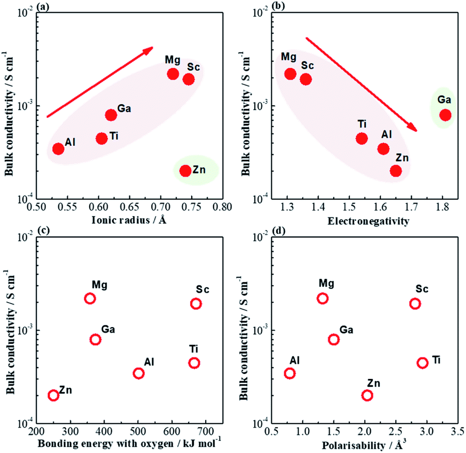 | ||
| Fig. 13 Bulk conductivity as a function of (a) ionic radius, (b) electronegativity, (c) bonding energy with oxygen and (d) polarisability of dopant ions. | ||
Among all the acceptor-doped NB0.51T ceramics in this study, the highest σb value (3 mS cm−1 at 500 °C) is obtained in Na0.5Bi0.51Ti1−xMgxO3.015−x for x = 0.02, which is slightly lower than the highest σb previously observed in Sr-doped NB0.49T (5.6 mS cm−1 at 500 °C). It can be concluded therefore that high oxide-ion conductivity can also be achieved by B-site acceptor-doping in an insulating NB0.51T.
Conclusion
The effect of acceptor-doping on the electrical conductivity and conduction mechanism of nominally Bi-excess sodium bismuth titanate, NB0.51T ceramics is investigated by impedance spectroscopy and electromotive force measurements. Five acceptor-type dopants including Mg2+, Zn2+, Sc3+, Ga3+ and Al3+ were selected to partially replace Ti4+ in NB0.51T. Acceptor-doping on the Ti-site changes the electrical behaviour of NB0.51T from insulating (type III) to mixed ionic–electronic conduction (type II) to oxide-ion conducting (type I). Most importantly, it is surprising to find that extremely low levels of acceptor-type dopants can introduce considerable levels of oxide-ion conduction into NB0.51T, i.e., 0.5% Mg-doping can enhance the bulk conductivity of NB0.51T more than 3 orders of magnitude and the oxide-ion transport number from <0.1 for NB0.51T to >0.9 at 600 °C. Furthermore, acceptor doping in NB0.51T changes the “onset” nominal oxygen deficiency for the insulating–conducting transition from δ = 0 to δ < 0. The intriguing electrical behaviours in acceptor-doped NB0.51T dielectrics is attributed to the ceramic microstructure. When the doping level is extremely low (i.e., 0.1% and 0.5% for divalent and trivalent dopants, respectively), NB0.51T ceramics develop an inhomogeneous microstructure with randomly distributed large grains embedded in a small grained matrix. Such ceramics can be approximated to a two-phase composite with large grains (d > 3.5 μm) as a non-percolative conductive phase and small grains (d < 3.5 μm) as the insulating phase. Statistics on the grain size show the fraction of the conductive, large grains in the ceramic agrees with the oxide-ion transport number. The electrical two-phase model is also supported by finite element modelling. Unlike that in NB0.50T and NB0.49T oxide-ion conductors, electrical conduction behaviour in acceptor-doped NB0.51T is a combined effect from defect chemistry and ceramic microstructure.This study not only confirms the effectiveness of using acceptor-doping to obtain high-oxide ion conductivity but also points out the significance of the ceramic microstructure on the electrical conduction behaviour in NBT-based materials. Furthermore, together with the previously reported results on acceptor-doped NB0.50T and NB0.49T, it can be summarized that dopants with large ionic radii are generally beneficial to oxide-ion conduction in NBT-based materials albeit Zn being an exception. This can be used as a criterion for selecting appropriate dopants to meet the electrical property requirements for different applications.
Conflicts of interest
There are no conflicts to declare.Acknowledgements
This work is supported by EPSRC (EP/L027348/1), National Natural Science Foundation of China (52072239, 22002089), Foundation of China-Excellent Young Scholars (51922068), Shanghai Pujiang Program (19PJ1404400). EPV would like to thank CONACYT for his scholarship under ‘‘Becas CONACYT al extranjero (registro 327115)’’and the University of Sheffield for financial support.References
- M. Li, M. J. Pietrowski, R. A. De Souza, H. Zhang, I. M. Reaney, S. N. Cook, J. A. Kilner and D. C. Sinclair, Nat. Mater., 2014, 13, 31 CrossRef CAS.
- L. Li, M. Li, H. Zhang, I. M. Reaney and D. C. Sinclair, J. Mater. Chem. C, 2016, 4, 5779 RSC.
- M. S. Islam, J. Mater. Chem., 2000, 10, 1027 RSC.
- M. Li, L. Li, J. Zang and D. C. Sinclair, Appl. Phys. Lett., 2015, 106, 102904 CrossRef.
- F. Yang, M. Li, L. Li, P. Wu, E. Pradal-Velázquez and D. C. Sinclair, J. Mater. Chem. A, 2018, 6, 5243 RSC.
- F. Yang, P. Wu and D. C. Sinclair, J. Mater. Chem. C, 2018, 6, 11598 RSC.
- F. Yang, P. Wu and D. C. Sinclair, J. Mater. Chem. C, 2017, 5, 7243 RSC.
- F. Yang, H. Zhang, L. Li, I. M. Reaney and D. C. Sinclair, Chem. Mater., 2016, 28, 5269 CrossRef CAS.
- K.-C. Meyer and K. Albe, J. Mater. Chem. A, 2017, 5, 4368 RSC.
- D. P. C. Shih, A. Aguadero and S. J. Skinner, Solid State Ionics, 2018, 317, 32 CrossRef CAS.
- R. Bhattacharyya and S. Omar, Solid State Ionics, 2018, 317, 115 CrossRef CAS.
- F. Yang, M. Li, L. Li, P. Wu, E. Pradal-Velázquez and D. C. Sinclair, J. Mater. Chem. A, 2017, 5, 21658 RSC.
- F. Yang, P. Wu and D. C. Sinclair, Solid State Ionics, 2017, 299, 38 CrossRef CAS.
- J. Huang, F. Zhu, D. Huang, B. Wang, T. Xu, X. Li, P. Fan, F. Xia, J. Xiao and H. Zhang, Ceram. Int., 2016, 42, 16798 CrossRef CAS.
- R. Bhattacharyya, S. Das and S. Omar, Acta Mater., 2018, 159, 8 CrossRef CAS.
- Y. Lu, C. A. López, J. Wang, J. A. Alonso and C. Sun, J. Alloys Compd., 2018, 752, 213 CrossRef CAS.
- Y. Zhang, J. Huang, H. Zhang, Q. Zhang and H. Fan, J. Mater. Sci.: Mater. Electron., 2019, 30, 17078 CrossRef CAS.
- R. Bhattacharyya and S. Omar, J. Alloys Compd., 2018, 746, 54 CrossRef CAS.
- R. A. De Souza, Adv. Funct. Mater., 2015, 25, 6326 CrossRef CAS.
- H. Zhang, A. H. H. Ramadan and R. A. De Souza, J. Mater. Chem. A, 2018, 6, 9116 RSC.
- J. S. Dean, J. H. Harding and D. C. Sinclair, J. Am. Ceram. Soc., 2014, 97, 885 CrossRef CAS.
- L. Li, PhD thesis, The University of Sheffield, 2017.
- F. Yang and D. C. Sinclair, unpublished results.
- D. K. Khatua, T. Mehrotra, A. Mishra, B. Majumdar, A. Senyshyn and R. Ranjan, Acta Mater., 2017, 134, 177 CrossRef CAS.
- X. Liu, Y. Zhao, H. Hu, H. Du and J. Shi, Ionics, 2019, 25, 2729 CrossRef CAS.
- X. Chen, J. Zeng, X. Yan, M. Zhou, P. Tang, T. Liang and W. Li, Solid State Ionics, 2017, 309, 152 CrossRef CAS.
- D. S. McLachlan, M. Blaskzkiewicz and R. E. Newnham, J. Am. Ceram. Soc., 1990, 73, 2187 CrossRef CAS.
- C. H. Rycroft, Chaos, 2009, 19, 041111 CrossRef.
- S. Faouria, A. Mostaed, J. S. Dean, D. Wang, D. C. Sinclair, S. Zhang, W. G. Whittow, Y. Vardaxoglou and I. M. Reaney, Acta Mater., 2019, 166, 202 CrossRef.
- Y. R. Luo, Comprehensive handbook of chemical bond energies, CRC Press, Boca Raton, FL, 2007 Search PubMed.
- N. M. Grimes and R. W. Grimes, J. Phys.: Condens. Matter, 1998, 10, 3029 CrossRef CAS.
Footnote |
| † Electronic supplementary information (ESI) available. See DOI: 10.1039/d0ta10071d |
| This journal is © The Royal Society of Chemistry 2020 |