
Plasmonic hole ejection involved in plasmon-induced charge separation
Tetsu
Tatsuma
 * and
Hiroyasu
Nishi
* and
Hiroyasu
Nishi
Institute of Industrial Science, The University of Tokyo, 4-6-1 Komaba, Meguro-ku, Tokyo 153-8505, Japan. E-mail: nishi-h@iis.u-tokyo.ac.jp; tatsuma@iis.u-tokyo.ac.jp
First published on 28th November 2019
Abstract
Since the finding of plasmon-induced charge separation (PICS) at the interface between a plasmonic metal nanoparticle and a semiconductor, which has been applied to photovoltaics including photodetectors, photocatalysis including water splitting, sensors and data storage in the visible/near-infrared ranges, injection of hot electrons (energetic electrons) into semiconductors has attracted attention almost exclusively. However, it has recently been found that behaviours of holes are also important. In this review, studies on the hot hole ejection from plasmonic nanoparticles are described comprehensively. Hole ejection from plasmonic nanoparticles on electron transport materials including n-type semiconductors allows oxidation reactions to take place at more positive potentials than those involved in a charge accumulation mechanism. Site-selective oxidation is also one of the characteristics of the hole ejection and is applied to photoinduced nanofabrication beyond the diffraction limit. Hole injection into hole transport materials including p-type semiconductors (HTMs) in solid-state cells, hole ejection through a HTM for stabilization of holes, hole ejection to a HTM for efficient hot electron ejection, voltage up-conversion by the use of hot carriers and electrochemically assisted hole ejection are also described.
 Tetsu Tatsuma | Tetsu Tatsuma received his BSc degree in 1988, MSc degree in 1990 and PhD degree in 1993 in electrochemistry from The University of Tokyo. He held the position of an Assistant Professor at Tokyo University of Agriculture and Technology before joining Prof. Akira Fujishima's group at The University of Tokyo as Lecturer in 1998. After promotion to an Associate Professor in 2000, he joined Institute of Industrial Science, The University of Tokyo in 2001. He has been a Full Professor since 2008. He received the Award for Creative Work from the Chemical Society of Japan in 2011, Award for Scientific Achievement from the Electrochemical Society of Japan in 2012 and The Japanese Photochemistry Association Award in 2014. His current research interests include photoelectrochemistry and nanophotonics related to plasmonics. |
 Hiroyasu Nishi | Hiroyasu Nishi received his BSc degree in 2007, MSc degree in 2009 and PhD degree in 2012 from Osaka City University. He joined Prof. Tsukasa Torimoto's group as a post-doc in 2012. Since 2013 he has been an Assistant Professor in Prof. Tetsu Tatsuma's group at the Institute of Industrial Science, The University of Tokyo. He received the Award for Young Scientists from the Electrochemical Society of Japan in 2019. His current research interests include photoelectrochemistry of plasmonic and semiconducting nanomaterials. |
1. Plasmon-induced charge separation (PICS)
Regardless of the very long history of plasmonic nanomaterials over 2000 years, they have been used actively in the field of nanoscience just for the last few decades. The plasmonic nanomaterials entrap photons effectively and convert those to plasmons, which are based on electron oscillation in resonance with electric field oscillation of light (localized surface plasmon resonance, LSPR). The plasmons thermally decay in a non-radiative manner in most cases, and the decay is observed as light absorption. Since the wavelength-selective absorption gives brilliant colours, the plasmonic nanomaterials have been applied to colouring of glassware and ceramics. If the plasmons are converted again to photons, the effect is observed as light scattering, which is based on radiative decay. In some other cases, the energy of the plasmons is transferred to non-plasmonic materials such as organic dyes and semiconductors via optical near field generated around the resonant nanomaterials. This process is used for “plasmonic enhancement” of conventional photophysical and photochemical processes including fluorescence, photovoltaics and photocatalysis.The application fields of the plasmonic nanomaterials expanded in the last decade, since direct conversion of plasmons to rectified electron flows was reported.1 This effect, plasmon-induced charge separation (PICS), is observed often at the interface between a plasmonic nanomaterial and a semiconductor. It has been applied to photovoltaics1,2 including near infrared photodetection, photocatalysis,1 chemical sensing and biosensing based on plasmonic responses to refractive index changes, storage of data and colour images based on multicolour photochromism, photoswitching of physical and chemical properties and photochemical nanofabrication beyond the diffraction limit.3 Introduction of a viewpoint of photocatalysis, which is based on electrochemistry and solid-state physics, to plasmonics led to the achievement of PICS.1
The most widely studied PICS system is based on Au nanoparticles (AuNPs) (or Ag nanoparticles, AgNPs) and TiO2 as an n-type semiconductor or an electron transport material (ETM).1,3,4 Therefore, the PICS mechanisms have been studied and discussed mainly for the AuNP–TiO2 and AgNP–TiO2 systems. PICS has been explained chiefly in terms of the external photoelectric effect, which involves transfer of energetic electrons (so-called hot electrons) from resonant plasmonic nanoparticles to TiO2,1 though some researchers speculated that TiO2 photocatalysis5 could be enhanced by plasmon resonance.6 The mechanistic studies were therefore focused on the possible electron transfer process in the early stage of the PICS studies. The electron transfer was proved by reversing the electrode/TiO2/AuNP structure, which gives anodic photocurrents,1 to the electrode/AuNP/TiO2 structure, which gives cathodic photocurrents.7,8 The photopotentials of single AuNPs on TiO2 were also measured by Kelvin probe force microscopy (KFM), and were found to be positive under plasmonic excitation.9
2. Anodic reactions and hole ejection involved in PICS
Since electrons are taken by TiO2, reduction reactions should proceed at TiO2, and oxidation reactions should take place at metal nanoparticles. In the case of AgNP–TiO2 systems, actually, AgNPs themselves are oxidized to Ag+ in PICS, indicating that AgNPs are oxidation sites.4 AuNPs on TiO2 are also oxidized and dissolved by PICS, in the presence of halide ions,10 which negatively shifts the thermodynamic potential of the Au oxidation. Oxidative polymerization of pyrrole to polypyrrole11,12 and oxidative deposition of PbO213–15 are also localized at AuNPs.There are two possible mechanisms of oxidation reactions at plasmonic metal nanoparticles: the charge accumulation mechanism and the hole ejection mechanism (Fig. 1). When a plasmon decays in a non-radiative manner, a hot electron–hole pair may be generated.16,17 The hot electron is ballistically transported in the nanoparticle and ejected from the nanoparticle if the energy of the hot electron is higher than the work function of the metal.16 In the case where the metal nanoparticle is in direct contact with a semiconductor, the hot electron could be injected into the semiconductor, if the energy of the electron is higher than the energy barrier at the nanoparticle–semiconductor interface. If the hole, left in the plasmonic metal nanoparticle, is not consumed by an oxidation reaction, it will be relaxed to the Fermi level. Here let us consider the case where the AuNP and TiO2, which are in direct contact with each other, are just soaked in a solution, which contains some electron donors and acceptors, like “common” solutions. The equilibrium potential of the solution, to which the potential of the AuNP–TiO2 composite is aligned, depends on the standard electrode potentials and activities of those chemical species.18 If the redox potential of a target species, which is desired to be oxidized, is more positive than the potential of the AuNP–TiO2 composite, the species is not oxidized. Rather, its oxidized form, if any, would be reduced.
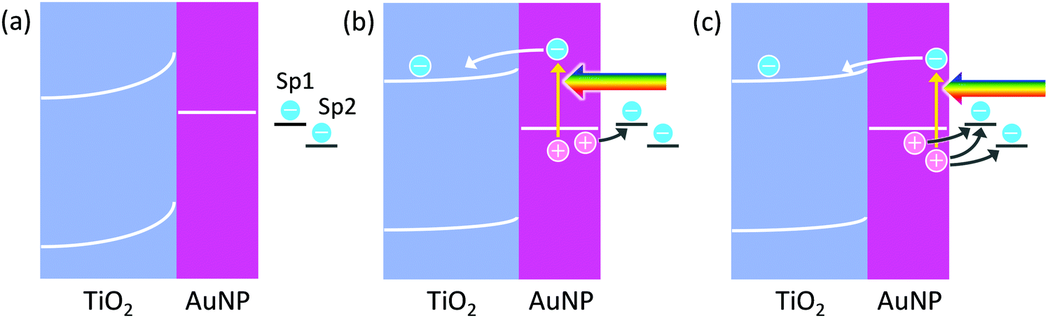 | ||
| Fig. 1 (a) Band structure of TiO2–AuNP systems. Schematics for electrochemical reactions based on (b) charge accumulation and (c) hole ejection. Note that the systems are close to an open circuit system. | ||
Among the chemical species contained in the solution, only two target species, Sp1 and Sp2 (redox-active species), are drawn in Fig. 1. Now, the composite is irradiated with light, and the AuNP is in the plasmon resonance state. As a result, hot electron–hole pairs are generated as described above. If the hot electrons of the pairs are injected into the TiO2 conduction band and accumulated in it, and the hot holes are relaxed and accumulated as positive charges in the AuNP, a potential difference would arise at the interface. If the potential of the AuNP is more positive than the potential of Sp1, it is oxidized at the AuNP surface. Note that the system is an open-circuit until a reaction occurs. Even if a reaction occurs, the system may be far away from the short-circuited state, although diagrams of a short-circuit state are often drawn.
However, if the generated hot hole contributes to oxidation reactions, before being relaxed to the Fermi level, oxidation reactions with more positive redox potential could proceed. This is hot hole ejection. The energetic hole of the electron–hole pair could be ejected from the plasmonic nanoparticle directly, or via a trap site, into a solution. The simplest hole ejection process could be ejection of metal ions from the metal nanoparticle; for instance, ejection of Ag+ from a plasmonic AgNP. Another typical process is hole transport from the nanoparticle to a hole acceptor (i.e. electron donor) in the solution. The other possible situation is ejection of a hole from the nanoparticle into a solid, typically a hole transport material such as a p-type semiconductor. Watanabe and Gerischer19,20 studied hole ejection from the oxidized, bulk Au surface into an aqueous solution.
In Fig. 1, Sp2 can be oxidized by the hole ejection, but not by the charge accumulation. The lifetimes of the hot holes are known to be very short. According to the calculation of Atwater and co-workers,21,22 holes below the Fermi level by <1.5 e V (potential more positive than the equilibrium potential of the AuNP by <1.5 V) have lifetimes of 10–40 fs (and the mean free path length of 10–50 nm). Therefore, temporal entrapment of the holes at surface redox sites including an impurity or defect levels or adsorption of the reaction species may be necessary for most of the oxidation reactions by hole ejection, in particular for multi-electron reactions.
3. Hole ejection for photocatalytic oxidation
In an ideal system, the height of the energy barrier at the AuNP–TiO2 interface is constant, EAu − ETiO2, where EAu and ETiO2 are the work function of Au and electron affinity of TiO2, respectively. If this holds for the real system, the photovoltage expected for the charge accumulation mechanism (VCA) equals the barrier height or is smaller (i.e. VCA ≤ (EAu − ETiO2)/e). In the case of the Au–TiO2 system, the value of the barrier height is 1.2 eV for theoretical evaluation and could be lower for nanoscale systems23,24 (e.g. ∼0.9 eV for experimental fitting).25 Considering that a certain overvoltage is necessary for oxidation and reduction of water, it should be difficult to drive water splitting by PICS of the Au–TiO2 system. However, Moskovits et al.26 and Tanaka et al.27 have reported that Au–TiO2 systems can drive photo-induced water splitting without electrical or chemical bias application. This suggests that hole ejection, in which the photovoltage (VHE) can be higher than EAu − ETiO2 and is limited by the energy of incident photons, EP (i.e. VHE ≤ EP/e), could contribute to the reactions. In the case of the AuNP–TiO2 systems, EP is typically ∼2 eV, which is sufficient for water splitting.Recently, in some photocatalytic systems based on PICS, possible contribution of energetic holes to oxidation reactions was discussed.13,15,28–30 However, in many cases, it is difficult to show direct evidence for this. Table 1 shows some of the oxidation reactions with relatively positive potentials driven by PICS. Note that the standard electrode potential E° is just one of the indicators for judging whether or not the reaction takes place. An electrochemical oxidation occurs when the electrode potential is more positive than the equilibrium potential of the system, which is given by the Nernst equation (E° − (RF/nT)ln(ared/aox), where ared and aox are the activities of the reduced and oxidized forms of the redox couple).18 In many cases, however, it is difficult to control the activity of reaction products, aox. Thus they often consider just the activity of the reaction species and pH.
| Reaction | E° (V vs. NHE) | Ref.a |
|---|---|---|
| a References reporting the reactions by PICS. b These reactions have not been reported for the AuNP–TiO2 systems. c Experimentally measured oxidation potential in CF3COOH.35 d EDOT = 3,4-ethylenedioxythiophene, PEDOT = polymer of EDOT. e Experimentally measured oxidation potential in 0.1 M TBAP/CH3CN.36 | ||
| Au + h+ → Au+ | +1.83 | —b |
| Au + 3h+ → Au3+ | +1.52 | —b |
| C6H6 + H2O + 2h+ → C6H5OH + 2H+ | (+2.4)c | 31 |
nEDOT + 2nh+ → PEDOT + 2nH+![[thin space (1/6-em)]](https://www.rsc.org/images/entities/char_2009.gif) d d |
(+1.8)e | 32 |
| Pb2+ + 2H2O + 2h+ → PbO2 + 4H+ | +1.47 | 13–15 |
| Au + 3H2O + 3h+ → Au(OH)3 +3H+ | +1.36 | 33 |
| 2H2O + 4h+ → O2 + 4H+ | +1.23 | 34 |
| Au + 4Cl− + 3h+ → [AuCl4]− | +1.00 | 10 |
| Au + 4Br− + 3h+ → [AuBr4]− | +0.85 | 10 |
| Ag + h+ → Ag+ | +0.80 | 4 |
Regarding the Ag–TiO2 systems, it is known that AgNPs dissolve under light irradiation.4 Therefore, oxidation reactions with the redox potential more negative than ∼+0.8 V could occur. In the case of the Au–TiO2 systems, AuNPs are known to be stable in most cases, hence the potential reachable by the holes is more negative than ∼+1.8 V, which is the potential for single-electron oxidation of Au to Au+. If the Au surface has hole trap sites that allow multi-electron oxidation of Au to Au3+, the limit value could be ∼+1.5 V. The actual potential value achieved in a well-defined system is ∼+1.3 V, for the PbO2 deposition at pH ∼ 2.15
One of the issues of the employment of the hole ejection for photocatalytic oxidation is the short lifetime of the holes, as described above. To address this issue, Liu and co-workers37 used very small Pt–Cu nanoparticles (2 nm in size) deposited on TiO2 for better efficiencies of hot electron injection into TiO2. They also consider that an alcohol molecule as a reaction species is adsorbed onto the particle surface and entraps the short-lived holes.
The population of the holes depends on the depth (or potential) of the holes. Willets and co-workers38 combined the Au–TiO2 system with scanning electrochemical microscopy (SECM) to examine the external quantum efficiency for oxidation of several redox probes, ferrocenemethanol, [Fe(CN)6]4−, a ferrocenyl methyl trimethylammonium ion and [IrCl6]3−, which undergo outer-sphere electrochemical reactions at different potentials. The results (Fig. 2a) show that the efficiency decreases as the potential of the redox probe shifts positively. They explained this tendency in terms of the decreasing population of hot holes that are available for the redox reactions (Fig. 2b).
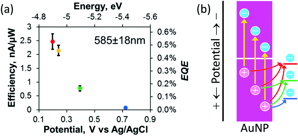 | ||
| Fig. 2 (a) Dependence of oxidation efficiency (or external quantum efficiency, EQE) for different redox species on their redox potential and (b) diagram for explanation of the dependence. Reproduced with permission from (a) ref. 38 ©2019 American Chemical Society. | ||
4. Hole ejection involved in solid-state cells
The hole ejection behaviour and potentials (or energy levels) of the holes could be examined by using solid-state photovoltaic cells with hole transport materials (HTMs): plasmonic NPs are deposited on an ETM, and coated with a HTM. The ETM–metal–HTM (or n-type–metal–p-type) cells will be referred to as E–M–H (or n–M–p) type cells hereafter. The authors prepared E–M–H type cells by depositing AuNPs on TiO2 and coating the AuNPs with a HTM, such as CuI, CuSCN, poly(N-vinylcarbazole) (PVK), N,N′-diphenyl-N,N′-bis(3-methylphenyl)-(1,1′-biphenyl)-4,4′-diamine (TPD) or 4,4-bis[N-(1-naphthyl)-N-phenyl-amino]biphenyl (NPD).39 The electron affinity and ionization energy values of those HTMs are summarized in Fig. 3 together with those values of some other HTMs and TiO2 and work function values of plasmonic metals.40–48 Since the ionization energy values of those HTMs are larger than the work function of Au (5.1 eV), there are energy barriers for holes at the AuNP–HTM interfaces (0.2–0.7 eV). Despite the energy barrier, these TiO2–AuNP–HTM type cells exhibit photocurrent responses as shown in Table 2, indicating that energetic holes are injected from the AuNPs to the HTMs. Mulvaney et al. pointed out the possibility of hole injection into HTMs.49 They used N2,N2,N2′,N2′,N7,N7,N7′,N7′-octakis(4-methoxyphenyl)-9,9′-spirobi[9H-fluorene]-2,2′,7,7′-tetramine (Spiro-OMe-TAD) as a HTM.49,50 Since the barrier height is very low (∼0.1–0.2 eV), even almost completely relaxed holes could be injected into the HTM. This may also hold when NiO51 or PEDOT:PSS55 (PSS = poly(styrenesulfonate)) is used as a HTM. The authors also used 4,4′,4′′-tri-9-carbazolyltriphenylamine (TCTA) and 4,4′-bis(9H-carbazol-9-yl)biphenyl (CBP) in addition to Spiro-OMe-TAD, PVK and TPD as HTMs. The hole injection was observed even for the cell with CBP, which has an energy barrier of ∼0.9 eV.56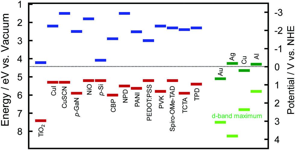 | ||
| Fig. 3 Electron affinity (blue) and ionization energy (red) values of selected HTMs including p-type semiconductors and TiO2 as a typical ETM or n-type semiconductor and work function (green) and d-band maximum (light green) values of major plasmonic metals, Au, Ag, Cu and Al.40–48 TCTA = 4,4′,4′′-tri-9-carbazolyltriphenylamined an CBP = 4,4′-bis(9H-carbazol-9-yl)biphenyl. See the text for other abbreviations. | ||
| Cell type | VOC (V) | IPCE (%) | Ref. |
|---|---|---|---|
| TiO2/AuNP/CuI | 0.28 | 0.00084 | 39 |
| TiO2/AuNP/CuSCN | 0.25 | 0.00063 | 39 |
| TiO2/AuNP/NPD | 0.26 | 0.00032 | 39 |
| TiO2/AuNP/PVK | 0.25 | 0.00024 (560 nm) | 39 |
| TiO2/AuNP/TPD | 0.15 | 0.00024 | 39 |
| TiO2/AuNP/Spiro | 0.12 | 1.8 (600 nm) | 49 |
| TiO2/AgNP/Spiro | 0.21 | 1.4 (460 nm) | 49 |
| 0.2–0.3 | 2.4 (620 nm) | 50 | |
| Nb–TiO2/AuNP/NiO | 0.73 | 0.1 (650 nm) | 51 |
| AuNP/PANI | 0.85 | 7 (450 nm) | 44 |
| AuNP/p-Si | ∼0.1 | — | 52 |
| AuNanogrid/p-GaN | 0.62 | 0.0004 (570 nm) | 53 |
| AuNanogrid/p-Si | — | — | 54 |
Besides the E–M–H type solid-state cells, M–H type (or M-p type) cells with simpler structures have also been developed (Table 2). Polyaniline (PANI) can serve as a HTM,44 which could also absorb light, if it is not completely reduced to an insulating state. When a p-Si is used as a HTM,52,54 the energy barrier is as low as 0.3–0.7 eV and the photocurrent responses can be obtained even at 1600 nm (corresponding to 0.78 eV). Atwater et al. used p-GaN as a HTM57 and prepared a cell with an energy barrier of 1.1 eV, which exhibits photocurrents in the visible range.53
Although metal nanoparticles (e.g. Au and Ag) have been used in most of the PICS studies, PICS has also been achieved by using plasmonic compound nanoparticles. Interestingly, it was not successful for long time, when only hot electron injection was targeted, but it was achieved by different groups for hole injection from the MoO3−x nanostructure to the TiO2 valence band58 and that from CuS nanoparticles to the valence band of CdS.59 Once compound PICS was attained by hole injection, it was soon achieved by electron injection as well.60,61
5. Site-selective hole ejection and nanofabrication beyond the diffraction limit
The plasmonic hole ejection involved in PICS can also be applied to photoelectrochemical nanofabrication beyond the diffraction limit. Plasmonic nanoparticles and nanostructures are often fabricated by top-down techniques including electron beam lithography (EBL).62 Although EBL allows nanostructures with well-designed morphologies and orientations to be developed, its resolution is not so high and is not suitable for the fabrication of three-dimensional structures. It takes time and cost, so that it is not appropriate for preparing samples with wide area. In order to address these issues, they use bottom-up methods.63 A plasmonic nanofabrication technique, in which plasmonic nanoparticles are modified and elaborated further by the aid of plasmonics, is included in the bottom-up methods, or hybrids of top-down and bottom-up methods.The plasmonic nanofabrication is based on selective excitation of one of the resonance modes by irradiation with light of the resonance wavelength or light of appropriate polarization. In the case of a nanorod, it exhibits a transverse mode and longitudinal mode, at shorter and longer wavelengths, respectively.64 The former mode is resonated with light polarized along the short axis of the nanorod. Electrons are also oscillated along the short axis, and electric field is localized at the sides of the nanorod. The latter mode is resonated with light polarized along the long axis and the electrons are also oscillated along the long axis. The electric field is localized at both of the tips of the nanorod.
Even in the case of a plasmonic nanoparticle exhibiting just one mode, irradiation with linearly polarized light with different polarization angles could cause electron oscillation in different angles and generate confined local electric fields at different sites. Chen and Osgood65 achieved anisotropic growth of plasmonic Cd nanoparticles by irradiation with linearly polarized light that causes plasmonic enhancement of the photodissociation of gaseous CdMe2 and deposition of Cd at local plasmon resonance sites (Fig. 4a). Selective growth of Ag nanodisks in in-plane and out-of-plane directions was also performed by selective resonance of the corresponding mode.73 Local deposition of Pt at Au nanoparticle oligomers74 and reductive polymerization of bisthienylbenzene at triangular Au nanoplates75 were also attained at resonance sites by irradiation with linearly polarized light. These local reduction reactions for unsupported plasmonic nanoparticles, which are not deposited on a solid substrate, are explained in terms of local generation of energetic electron–hole pairs76 and ejection of hot electrons77 at plasmon resonance sites. Even so, oxidation reaction sites have not been known for those unsupported nanoparticles, to the best of our knowledge.
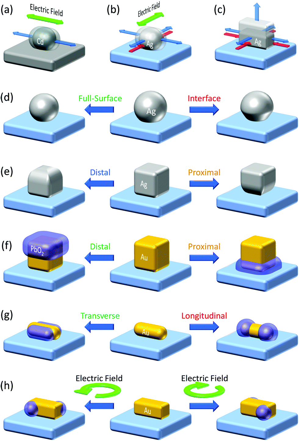 | ||
| Fig. 4 Plasmonic nanofabrication. (a) Anisotropic growth of Cd nanoparticles on carbon.65 (b) Anisotropic growth of Ag nanoparticles on TiO2.66,67 (c) Vertical growth of Ag nanocuboids on TiO2.68 (d) Size and shape changes of Ag (and Au) nanospheres on TiO2.69,70 (e) Site-selective etching of Ag nanocubes on TiO2.71 (f) Site-selective deposition of PbO2 on Au nanocubes on TiO2.14 (g) Site-selective deposition of PbO2 on Au nanorods on TiO2.14 (h) Preparation of chiral plasmonic nanostructures by circularly polarized light.72 Colours of the text correspond to those of the resonance light. | ||
In the studies of PICS for Ag–TiO2 systems, the authors found that Ag oxidation to Ag+ involved in PICS occurs selectively at resonance sites.78 This effect was used for aspect-ratio-selective (i.e. resonance-wavelength-selective) reversible shortening and re-elongation of Ag nanorods on TiO2 and applied to near infrared photochromism.79 The oxidation occurring at the resonance site was exploited for orientation control of Ag nanoparticles. When an ensemble of Ag nanoparticles is grown by photocatalytic reduction of Ag+ on UV-irradiated TiO2 (Fig. 4b, blue arrows), the growth in one direction was suppressed by the Ag oxidation under light polarized in the direction (red arrows), resulting in preferential growth in the orthogonal direction.66,67 Upright Ag nanoplates in a certain direction were removed also by linearly polarized light.80,81 Suppression of the growth of Ag nanocuboids in the lateral direction (Fig. 4c, red arrows) resulted in the vertical growth.68
Selective excitation of the full-surface or interface mode of large spherical Ag nanoparticles (∼100 nm)69 or Au nanoparticles (∼150 nm)70 on TiO2 allowed the particles to be etched at the whole surface or the interfacial region, respectively (Fig. 4d). Likewise, selective excitation of the distal or proximal mode of Ag nanocubes gave rise to selective etching at the top or bottom face of the nanocubes (Fig. 4e).71 This was not explained by the thermal deformation, but by the hole ejection (Fig. 5a).82 The hole ejection was also applied to the selective deposition of PbO2 at the top or bottom region of Au nanocubes (Fig. 4f) and sides and tips of Au nanorods (Fig. 4g).14
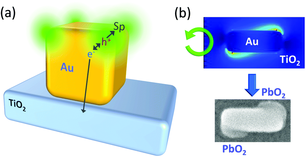 | ||
| Fig. 5 Hole ejection for site-selective oxidation. (a) Excitation of the distal mode of a Au nanocube on TiO2. (b) Electric field distribution around a Au nanocuboid on TiO2 under CPL and deposition of PbO2 at the resonance sites for the preparation of a chiral plasmonic nanostructure. Reproduced with permission from (b) ref. 72 ©2018 American Chemical Society. | ||
Since PbO2 is a dielectric material, which enhances plasmon resonance, the plasmonic properties of a nanoparticle can be modified by depositing PbO2 at specific sites. Okamoto et al.83 irradiated Au nanocuboids with circularly polarized light (CPL), and found that the electric field distribution under right CPL is the mirror image of that under left CPL. We therefore prepared an ensemble of Au nanocuboids on TiO2 and deposited PbO2 onto the cuboids by the hole ejection at resonance sites under CPL. As a result, chiral plasmonic nanostructures were obtained, and handedness of the nanostructures were selected by irradiating right or left CPL (Fig. 4h and 5b).72
This technique would also be used for more sophisticated plasmonic nanodevices including photocatalysts with enhanced activities and selectivity by introducing co-catalysts, charge accumulators or adsorbents on both anodic and cathodic sites.
6. Hole ejection through a HTM for stabilization of holes
The hole ejection mechanism allows oxidation reactions to occur at more positive potentials than the charge accumulation mechanism. However, the lifetimes of the holes are known to be so short (<100 fs), as mentioned above, that some oxidation reactions may not take place even if the potentials of the holes are more positive than the redox potentials of these reactions. In this case, they use HTMs including p-type semiconductors so as to “pin” the potential of the holes to the HOMO level or valence band level of the HTM used (Fig. 6). This would extend the lifetime of holes and therefore be advantageous in particular for slow reactions. In addition, since some HTMs can accumulate positive charges in themselves at the HOMO or valence band levels to some extent, multi-electron oxidation reactions would be promoted.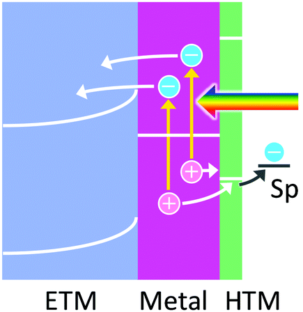 | ||
| Fig. 6 Hole trapping by a thin HTM to keep the potential of holes for the oxidation of a chemical species. | ||
An oxygen-evolving compound based on a cobalt oxide (Co-OEC)84,85 was deposited on Au nanoparticles of a Au–TiO2 system, and oxidation of water to oxygen was achieved.26,86 Au nanoparticles deposited on TiO2 were also coated with NiO,87 Ni(OH)2 or Cr2O3.88 These materials behave as p-type semiconductors, and accept holes (or relaxed positive charges in particular for NiO) from Au nanoparticles. Because the positive charges are accumulated in the HTMs, these materials promote multi-electron oxidation of water, for instance. It is also possible to deposit oxidation co-catalysts like Pt nanoparticles on the HTMs, if necessary, to accelerate the target reactions and to enhance the reaction selectivity.87 Among the HTMs, Ni(OH)2 is used as a cathode material for secondary batteries and has high redox activity that allows it to store positive charges stably. It is therefore used for photocatalysts that can store an oxidizing ability.89 Likewise, the TiO2/AuNP/Ni(OH)2 system can be applied to a photoanode with an energy storage ability.88
For the hole trapping system, not only the energy level for trapping but also the compactness and thinness of the HTM layer should also be important, to entrap holes efficiently and to avoid losing the potential of holes due to voltage drop (i.e. IR-drop).
7. Hole ejection to a HTM for efficient hot electron ejection
Efficient collection of holes by HTMs including p-type semiconductors is expected to enhance the lifetimes of hot electrons and promote direct use of hot electrons at plasmonic nanoparticles, which allows reduction reactions to take place at potentials more negative than those for reduction reactions occurring via an ETM (e.g. TiO2) (Fig. 7). Thomann and co-workers90 deposited Au nanoparticles on p-NiOx as a p-type semiconductor and reported direct reduction of H+ to H2 by hot electrons in the nanoparticles. Similar M–H (or M-p) systems, such as p-BiOCl with Ag nanoparticles91 and Ni(OH)2 with Au nanoparticles,92 were reported, although reduction reactions were not well focused. A system with p-GaN and Au nanoparticles,53 which forms 1.1 eV Schottky barrier at the interface, was also fabricated for reduction of CO2, but a relatively large bias voltage was applied for driving the reaction.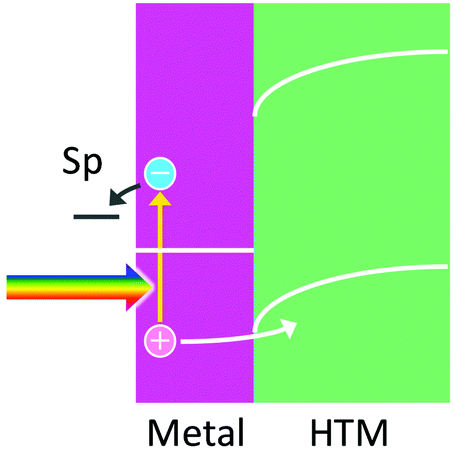 | ||
| Fig. 7 Hole ejection from a metal nanoparticle to a HTM for hot electron ejection to reduce a chemical species. | ||
For the M–H systems, further design of the system may be necessary, for rectification of holes. Although high barriers suppress back transfer of holes to metal nanoparticles, they limit the probability of hole transfer to the HTM.
8. Voltage up-conversion by hot carriers
Naik and Dionne93,94 designed a photon up-conversion system by combining Au nanodisks with InGaN (Fig. 8a). This system is based on the stepwise electron–hole injection. A hot electron from one electron–hole pair is injected into the conduction band of InGaN through a thin GaN layer. A hot hole is also injected from another electron–hole pair into the valence band of InGaN. Recombination of the electron in the conduction band and the hole in the valence band of the InGaN layer results in the emission of a photon, whose energy (2.8 eV) is higher than that of each incident photon (2.4 eV). The residual hole of the former electron–hole pair and the electron of the latter pair may recombine, possibly after relaxation.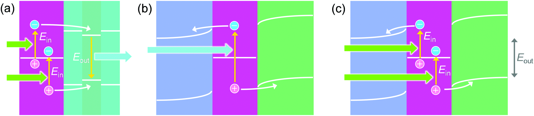 | ||
| Fig. 8 (a) Stepwise injection of electrons and holes to the intrinsic semiconductor for photon up-conversion (Eout > Ein). (b) Simultaneous injection of electrons and holes to the ETM and the HTM, respectively. (c) Stepwise injection of electrons and holes to the ETM and the HTM, respectively, for voltage up-conversion (Eout > Ein). | ||
For E–M–H (or n–M–p) systems, the charge separation is often illustrated as a one-photon process involving simultaneous injection of an electron into the ETM and a hole into the HTM from one hot electron–hole pair (Fig. 8b).39,49 However, a two-photon process involving stepwise injection of an electron from one electron–hole pair to the ETM and a hole from another pair to the HTM is also possible. A TiO2–AuNP–CBP cell exhibits photocurrents even if the energy of each incident photon (e.g. 1.8 eV) is lower than the energy gap between the conduction band level of TiO2 and the HOMO level of CBP (e.g. 2.1 eV).56 The stepwise injection is advantageous for low interfacial barriers. There is even a possibility of voltage up-conversion (Fig. 8c); the output voltage of the cell (Eout) could be higher than that expected for the incident photon energy (Ein).
9. Hole ejection from NPs on an electrode
When Au nanoparticles are deposited on an ITO electrode, photocurrents can be observed,95 but the currents are much lower than that for the AuNP–TiO2 system.96 Feldheim et al.95 explained the photocurrents in terms of a thermal effect. Recently, Xia and co-workers deposited Au nanoparticles including nanorods, nanostars and nanoplates on a glassy carbon electrode and reported that oxidation currents for glucose97 and ascorbic acid98 are enhanced under light irradiation. Willets and co-workers99 employed Au nanoparticles supported on an ITO electrode and observed photoinduced current enhancement for oxidation of [Fe(CN)6]4− and reduction of [Fe(CN)6]3− by using SECM, and suggested that both the hot carrier effects and the thermal effects contribute to the current enhancement. Link, Landes and co-workers100 deposited Au nanorods on an ITO electrode and observed oxidative dissolution of Au nanorods themselves. The onset potential for the dissolution was negatively shifted under light illumination by ∼0.05 V (Fig. 9a). Pensa et al.101 supported Au nanoparticles on an ITO electrode and monitored oxidation of aniline to PANI. Light irradiation shifted the onset potential for the polymerization negatively by ∼0.2 V (Fig. 9b). They explained these shifts of the onset potential in terms of the contribution of holes to the oxidation reactions. As shown in Fig. 9c, oxidation occurs only when the electrode potential is more positive than the redox potential of the redox species (Sp in the figure), in the conventional electrochemical systems. However, in the plasmonic systems, oxidation may occur even at a potential more negative than the redox potential, by the aid of the holes.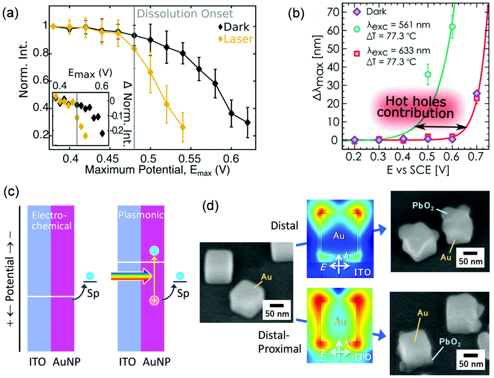 | ||
| Fig. 9 Negative shifts of onset potentials for (a) AuNP dissolution and (b) aniline polymerization by plasmon resonance and (c) the mechanism of the shifts. (d) Site-selective oxidation (PbO2 deposition) at Au nanocubes on a potential-controlled ITO electrode. Reproduced with permission from (a) ref. 100 and (b) ref. 101 ©2019 American Chemical Society and (d) ref. 102 © The Royal Society of Chemistry. | ||
The authors demonstrated site-selective oxidation by using Au nanorods and Au nanocubes adsorbed on an ITO electrode (Fig. 9d).102 Site-selective oxidation of Pb2+ to PbO2 at resonance sites is possible at certain potentials by selective excitation of one of the transverse or longitudinal modes of nanorods or the distal or proximal mode of nanocubes, as is the case for the AuNP–TiO2 system. Since the nanoscale local reactions cannot be explained in terms of a local thermal effect,82 the reactions are likely due to site-selective hole ejection. The deposition potential is negatively shifted by ∼0.05 V under light irradiation. Since the PbO2 deposition decreases the overvoltage needed for the Pb2+ oxidation, the initial PbO2 deposition accelerates further deposition. Oxidative dissolution of Au nanocubes can also be performed in a site-selective manner.102
10. Conclusions and outlook
Since hot holes are short-lived, their trap sites might be essential, although the trap sites have not yet been studied. The genuine Au surface could entrap positive charges in aqueous media if OH− is adsorbed onto it, by a reaction such as Au–OH− + h+ → Au(I)–OH. The adsorption of a reaction species itself could also be important for local trapping of holes. Studies and design of the trap sites, including introduction of HTMs into the PICS system for charge accumulation and driving multi-electron oxidation, are therefore important.It is reported that more energy of incident photons is distributed to hot holes than to hot electrons for Au and Cu, in particular at shorter wavelengths.21,22 In other words, hot holes are more energetic than hot electrons in Au and Cu. This is explained in terms of interband transitions, in which electrons in the deep 5d band are excited and holes are generated in the 5d band. Thus, the utilization of 5d band holes, rather than sp band holes, would improve the efficiency or the oxidation ability, in terms of potential, of holes. However, the lifetime and mean free path length of holes decrease as the energy of a hole increases. Therefore, control of the resonance sites, at which hot electron–hole pairs are generated, or nanoparticle size would be important for the efficient use of holes, in particular the deep 5d holes.
In order to design more sophisticated PICS systems, theoretical calculations of light absorption and charge separation behaviours is essential. Although the optical properties of the nanoparticles can be predicted at high accuracy and precision, it is still not easy to calculate the charge separation behaviour. Most recently, the separation behaviours of hot electrons and holes were calculated for cluster size nanoparticles and semiconductors in 1–2 nm in size (e.g. Ag20, Ag147 and Cd33Se33).103,104 However, metal clusters exhibit HOMO–LUMO based absorption, which is often stronger than plasmonic absorption, and electron injection from the LUMO to the TiO2 conduction band occurs efficiently.105 Therefore, calculation for larger, more plasmonic nanoparticles is awaited for more precise information about PICS including hole ejection.
Studies on hole ejection has just begun. It would enable oxidation reactions at more positive potentials, site-selective reactions and higher photovoltage output in PICS processes and devices. Further studies are expected to elucidate PICS mechanisms and lead to a wide variety of applications.
Conflicts of interest
There are no conflicts to declare.Acknowledgements
This work was supported in part by a Grant-in-Aid for Scientific Research (A) (No. JP16H02082).References
- Y. Tian and T. Tatsuma, J. Am. Chem. Soc., 2005, 127, 7632 CrossRef CAS PubMed.
- Y. Takahashi and T. Tatsuma, Appl. Phys. Lett., 2011, 99, 182110 CrossRef.
- T. Tatsuma, H. Nishi and T. Ishida, Chem. Sci., 2017, 8, 3325 RSC.
- Y. Ohko, T. Tatsuma, T. Fujii, K. Naoi, C. Niwa, Y. Kubota and A. Fujishima, Nat. Mater., 2003, 2, 29 CrossRef CAS.
- A. Fujishima and K. Honda, Nature, 1972, 238, 37 CrossRef CAS PubMed.
- W. Hou, W. H. Hung, P. Pavaskar, A. Goeppert, M. Aykol and S. B. Cronin, ACS Catal., 2011, 1, 929 CrossRef CAS.
- N. Sakai, Y. Fujiwara, Y. Takahashi and T. Tatsuma, ChemPhysChem, 2009, 10, 766 CrossRef CAS PubMed.
- W. Lee, J. Navarrete, B. Evanko, G. D. Stucky, S. Mubeen and M. Moskovits, Chem. Commun., 2016, 52, 13460 RSC.
- E. Kazuma and T. Tatsuma, Adv. Mater. Interfaces, 2014, 1, 1400066 CrossRef.
- Y. Konishi, I. Tanabe and T. Tatsuma, Dalton Trans., 2013, 42, 15937 RSC.
- Y. Takahashi, Y. Furukawa, T. Ishida and S. Yamada, Nanoscale, 2016, 8, 8520 RSC.
- H. Minamimoto, T. Tada, R. Futashima, X. Li, K. Suzuki, S. Yasuda and K. Murakoshi, J. Phys. Chem. C, 2016, 120, 16051 CrossRef CAS.
- S. Wang, Y. Gao, S. Miao, T. Liu, L. Mu, R. Li, F. Fan and C. Li, J. Am. Chem. Soc., 2017, 139, 11771 CrossRef CAS PubMed.
- H. Nishi, M. Sakamoto and T. Tatsuma, Chem. Commun., 2018, 54, 11741 RSC.
- J. Boltersdorf, G. T. Forcherio, J. P. McClure, D. R. Baker, A. C. Leff and C. Lundgren, J. Phys. Chem. C, 2018, 122, 28934 CrossRef CAS.
- J. G. Endriz and W. E. Spicer, Phys. Rev. Lett., 1970, 24, 64 CrossRef CAS.
- C. Sönnichsen, T. Franzl, T. Wilk, G. von Plessen, J. Feldmann, O. Wilson and P. Mulvaney, Phys. Rev. Lett., 2002, 88, 077402 CrossRef PubMed.
- T. Watanabe and H. Gerischer, J. Electroanal. Chem., 1981, 117, 185 CrossRef CAS.
- T. Watanabe and H. Gerischer, J. Electroanal. Chem., 1981, 122, 173 CrossRef.
- A. J. Bard and L. R. Faulkner, Electrochemical Methods, 2nd edn, Wiley, 2001 Search PubMed.
- R. Sundararaman, P. Narang, A. S. Jermyn, W. A. Goddard and H. A. Atwater, Nat. Commun., 2014, 5, 5788 CrossRef CAS PubMed.
- A. M. Brown, R. Sundararaman, P. Narang, W. A. Goddard III and H. A. Atwater, ACS Nano, 2016, 10, 957 CrossRef CAS PubMed.
- Y. Zhang, O. Pluchery, L. Caillard, A.-F. Lamic-Humblot, S. Casale, Y. J. Chabal and M. Salmeron, Nano Lett., 2015, 15, 51 CrossRef CAS PubMed.
- Z. Lin, X. Wang, J. Liu, Z. Tian, L. Dai, B. He, C. Han, Y. Wu, Z. Zeng and Z. Hu, Nanoscale, 2015, 7, 4114 RSC.
- H. Nishi and T. Tatsuma, J. Phys. Chem. C, 2018, 122, 2330 CrossRef CAS.
- S. Mubeen, J. Lee, N. Singh, S. Krämer, G. D. Stucky and M. Moskovits, Nat. Nanotechnol., 2013, 8, 247 CrossRef CAS PubMed.
- A. Tanaka, K. Teramura, S. Hosokawa, H. Kominami and T. Tanaka, Chem. Sci., 2017, 8, 2574 RSC.
- S. Sarina, E. Jaatinen, Q. Xiao, Y. M. Huang, P. Christopher, J. C. Zhao and H. Y. Zhu, J. Phys. Chem. Lett., 2017, 8, 2526 CrossRef CAS PubMed.
- H. Li, F. Qin, Z. Yang, X. Cui, J. Wang and L. Zhang, J. Am. Chem. Soc., 2017, 139, 3513 CrossRef CAS PubMed.
- C. Zhan, Z.-Y. Wang, X.-G. Zhang, X.-J. Chen, Y.-F. Huang, S. Hu, J.-F. Li, D.-Y. Wu, M. Moskovits and Z.-Q. Tian, J. Am. Chem. Soc., 2019, 141, 8053 CrossRef CAS PubMed.
- Y. Ide, M. Matsuoka and M. Ogawa, J. Am. Chem. Soc., 2010, 132, 16762 CrossRef CAS PubMed.
- Y. Takahashi, Y. Furukawa, Y. Sota, T. Ishida and S. Yamada, ECS Meeting Abstracts, 2016, MA2016-02, 3366.
- H. Nishi and T. Tatsuma, Angew. Chem., Int. Ed., 2016, 55, 10771 CrossRef CAS PubMed.
- C. G. Silva, R. Juarez, T. Marino, R. Molinari and H. Garcıa, J. Am. Chem. Soc., 2011, 133, 595 CrossRef PubMed.
- K. Fujimoto, Y. Tokuda, H. Maekawa, Y. Matsubara, T. Mizuno and I. Nishiguchi, Tetrahedron, 1996, 52, 3889 CrossRef CAS.
- B. Sankaran and J. R. Reynolds, Macromolecules, 1997, 30, 2582 CrossRef CAS.
- L. Zhang, C. Jia, S. He, Y. Zhu, Y. Wang, Z. Zhao, X. Gao, X. Zhang, Y. Sang, D. Zhang, X. Xu and H. Liu, Adv. Sci., 2017, 4, 1600448 CrossRef PubMed.
- Y. Yu, K. D. Wijesekara, X. Xi and K. A. Willets, ACS Nano, 2019, 13, 3629 CrossRef CAS PubMed.
- K. Yu, N. Sakai and T. Tatsuma, Electrochemistry, 2008, 76, 161 CrossRef CAS.
- Y. Xu and M. A. A. Schoonen, Am. Mineral., 2000, 85, 543 CrossRef CAS.
- M. Ye, C. He, J. Iocozzia, X. Liu, X. Cui, X. Meng, M. Rager, X. Hong, X. Liu and Z. Lin, J. Phys. D: Appl. Phys., 2017, 50, 373002 CrossRef.
- A. Wan, J. Hwang, F. Amy and A. Kahn, Org. Electron., 2005, 6, 47 CrossRef CAS.
- M. D. Ho, D. Kim, N. Kim, S. M. Cho and H. Chae, ACS Appl. Mater. Interfaces, 2013, 5, 12369 CrossRef CAS PubMed.
- T. Barman, A. A. Hussain, B. Sharma and A. R. Pal, Sci. Rep., 2015, 5, 18276 CrossRef CAS PubMed.
- L. Hao, Y. Liu, W. Gao, Z. Han, Q. Xue, H. Zeng, Z. Wu, J. Zhu and W. Zhang, J. Appl. Phys., 2015, 117, 114502 CrossRef.
- H. B. Michaelson, J. Appl. Phys., 1977, 48, 4729 CrossRef CAS.
- G. L. Eesley, Phys. Rev. B: Condens. Matter Mater. Phys., 1986, 33, 2144 CrossRef CAS.
- D. Gérard and S. K. Gray, J. Phys. D: Appl. Phys., 2015, 48, 184001 CrossRef.
- P. Reineck, G. P. Lee, D. Brick, M. Karg and P. Mulvaney, Adv. Mater., 2012, 24, 4750 CrossRef CAS PubMed.
- P. Reineck, D. Brick, P. Mulvaney and U. Bach, J. Phys. Chem. Lett., 2016, 7, 4137 CrossRef CAS PubMed.
- K. Nakamura, T. Oshikiri, K. Ueno, Y. Wang, Y. Kamata, Y. Kotake and H. Misawa, J. Phys. Chem. Lett., 2016, 7, 1004 CrossRef CAS PubMed.
- M. Alavirad, A. Olivier, L. Roy and P. Berini, Opt. Express, 2016, 24, 22544 CrossRef CAS PubMed.
- J. S. DuChene, G. Tagliabue, A. J. Welch, W.-H. Cheng and H. A. Atwater, Nano Lett., 2018, 18, 2545 CrossRef CAS PubMed.
- T. Matsui, Y. Li, M.-H. M. Hsu, C. Merckling, R. F. Oulton, L. F. Cohen and S. A. Maier, Adv. Funct. Mater., 2018, 28, 1705829 CrossRef.
- Y. Hattori, M. Abdellah, J. Meng, K. Zheng and J. Sa, J. Phys. Chem. Lett., 2019, 10, 3140 CrossRef CAS PubMed.
- T. Ishida, S. Toe and T. Tatsuma, J. Phys. Chem. C DOI:10.1021/acs.jpcc.9b08923.
- G. Tagliabue, J. S. DuChene, M. Abdellah, A. Habib, Y. Hattori, K. Zheng, S. E. Canton, D. J. Gosztola, W.-H. Cheng, R. Sundararaman, J. Sá and H. A. Atwater, 2018, arXiv:1810.04238 [cond-mat.mes-hall].
- S. H. Lee, H. Nishi and T. Tatsuma, Nanoscale, 2018, 10, 2841 RSC.
- Z. Lian, M. Sakamoto, H. Matsunaga, J. J. M. Vequizo, A. Yamakata, M. Haruta, H. Kurata, W. Ota, T. Sato and T. Teranishi, Nat. Commun., 2018, 9, 2314 CrossRef PubMed.
- M. Sakamoto, T. Kawawaki, M. Kimura, T. Yoshinaga, J. J. M. Vequizo, H. Mitsunaga, C. S. Ranasinghe, A. Yamakata, H. Matsuzaki, A. Furube and T. Teranishi, Nat. Commun., 2019, 10, 406 CrossRef PubMed.
- S. H. Lee, H. Nishi and T. Tatsuma, Phys. Chem. Chem. Phys., 2019, 21, 5674 RSC.
- T. Lee, J. Jang, H. Jeong and J. Rho, Nano Convergence, 2018, 5, 1 CrossRef CAS.
- Y. Xia, K. D. Gilroy, H.-C. Peng and X. Xia, Angew. Chem., Int. Ed., 2017, 56, 60 CrossRef CAS PubMed.
- X. Huang, S. Neretina and M. A. El-Sayed, Adv. Mater., 2009, 21, 4880 CrossRef CAS.
- C. J. Chen and R. M. Osgood, Phys. Rev. Lett., 1983, 50, 1705 CrossRef CAS.
- K. Matsubara, K. L. Kelly, N. Sakai and T. Tatsuma, J. Mater. Chem., 2009, 19, 5526 RSC.
- X. Wu and T. Tatsuma, Electrochemistry, 2011, 79, 773 CrossRef CAS.
- K. Saito and T. Tatsuma, Nanoscale, 2017, 9, 18624 RSC.
- I. Tanabe and T. Tatsuma, Nano Lett., 2012, 12, 5418 CrossRef CAS PubMed.
- I. Tanabe and T. Tatsuma, Chem. Lett., 2014, 43, 931 CrossRef CAS.
- K. Saito, I. Tanabe and T. Tatsuma, J. Phys. Chem. Lett., 2016, 7, 4363 CrossRef CAS PubMed.
- K. Saito and T. Tatsuma, Nano Lett., 2018, 18, 3209 CrossRef CAS PubMed.
- M. Maillard, P. Huang and L. Brus, Nano Lett., 2003, 3, 1611 CrossRef CAS.
- N. H. Kim, C. D. Meinhart and M. Moskovits, J. Phys. Chem. C, 2016, 120, 6750 CrossRef CAS.
- V.-Q. Nguyen, Y. Ai, P. Martin and J.-C. Lacroix, ACS Omega, 2017, 2, 1947 CrossRef CAS PubMed.
- H. Zhang and A. O. Govorov, J. Phys. Chem. C, 2014, 118, 7606 CrossRef CAS.
- C. Xue, G. S. Métraux, J. E. Millstone and C. A. Mirkin, J. Am. Chem. Soc., 2008, 130, 8337 CrossRef CAS PubMed.
- E. Kazuma, N. Sakai and T. Tatsuma, Chem. Commun., 2011, 47, 5777 RSC.
- E. Kazuma and T. Tatsuma, Chem. Commun., 2012, 48, 1733 RSC.
- I. Tanabe, K. Matsubara, N. Sakai and T. Tatsuma, J. Phys. Chem. C, 2011, 115, 1695 CrossRef CAS.
- Y. Sakai, I. Tanabe and T. Tatsuma, Nanoscale, 2011, 3, 4101 RSC.
- K. Saito, K. Setoura, S. Ito, H. Miyasaka, Y. Mitsuda and T. Tatsuma, ACS Appl. Mater. Interfaces, 2017, 9, 11064 CrossRef CAS PubMed.
- S. Hashiyada, T. Narushima and H. Okamoto, J. Phys. Chem. C, 2014, 118, 22229 CrossRef CAS.
- M. W. Kanan and D. G. Nocera, Science, 2008, 321, 1072 CrossRef CAS PubMed.
- Y. Surendranath, M. W. Kanan and D. G. Nocera, J. Am. Chem. Soc., 2010, 132, 16501 CrossRef CAS PubMed.
- J. Kim, H. Y. Son and Y. S. Nam, Sci. Rep., 2018, 8, 10464 CrossRef PubMed.
- K.-C. Kao, Y. Kuroiwa, H. Nishi and T. Tatsuma, Phys. Chem. Chem. Phys., 2017, 19, 31429 RSC.
- K.-C. Kao, H. Nishi and T. Tatsuma, ChemNanoMat, 2019, 5, 1021 CrossRef CAS.
- Y. Takahashi and T. Tatsuma, Langmuir, 2005, 21, 12357 CrossRef CAS PubMed.
- H. Robatjazi, S. M. Bahauddin, C. Doiron and I. Thomann, Nano Lett., 2015, 15, 6155 CrossRef CAS PubMed.
- S. Bai, X. Li, Q. Kong, R. Long, C. Wang, J. Jiang and Y. Xiong, Adv. Mater., 2015, 27, 3444 CrossRef CAS PubMed.
- G. Liu, P. Li, G. Zhao, X. Wang, J. Kong, H. Liu, H. Zhang, K. Chang, X. Meng, T. Kako and J. Ye, J. Am. Chem. Soc., 2016, 138, 9128 CrossRef CAS PubMed.
- G. V. Naik and J. A. Dionne, Appl. Phys. Lett., 2015, 107, 133902 CrossRef.
- G. V. Naik, A. J. Welch, J. A. Briggs, M. L. Solomon and J. A. Dionne, Nano Lett., 2017, 17(8), 4583 CrossRef CAS PubMed.
- L. B. Lowe, S. H. Brewer, S. Krämer, R. R. Fuierer, G. Qian, C. O. Agbasi-Porter, S. Moses, S. Franzen and D. L. Feldheim, J. Am. Chem. Soc., 2003, 125, 14258 CrossRef CAS PubMed.
- K. Kawahara, K. Suzuki, Y. Ohko and T. Tatsuma, Phys. Chem. Chem. Phys., 2005, 7, 3851 RSC.
- C. Wang, X.-G. Nie, Y. Shi, Y. Zhou, J.-J. Xu, X.-H. Xia and H.-Y. Chen, ACS Nano, 2017, 11, 5897 CrossRef CAS.
- C. Wang, X.-P. Zhao, Q.-Y. Xu, X.-G. Nie, M. R. Younis, W.-Y. Liu and X.-H. Xia, ACS Appl. Nano Mater., 2018, 1, 5805 CrossRef CAS.
- Y. Yu, V. Sundaresan and K. A. Willets, J. Phys. Chem. C, 2018, 122, 5040 CrossRef CAS.
- A. Al-Zubeidi, B. S. Hoener, S. S. E. Collins, W. Wang, S. R. Kirchner, S. A. H. Jebeli, A. Joplin, W.-S. Chang, S. Link and C. F. Landes, Nano Lett., 2019, 19, 1301 CrossRef.
- E. Pensa, J. Gargiulo, A. Lauri, S. Schlücker, E. Cortés and S. A. Maier, Nano Lett., 2019, 19, 1867 CrossRef CAS PubMed.
- H. Nishi and T. Tatsuma, Nanoscale, 2019, 11, 19455 RSC.
- J. Ma and S. Gao, ACS Nano DOI:10.1021/acsnano.9b03555.
- P. V. Kumar, T. P. Rossi, D. Marti-Dafcik, D. Reichmuth, M. Kuisma, P. Erhart, M. J. Puska and D. J. Norris, ACS Nano, 2019, 13, 3188 CrossRef CAS.
- N. Sakai and T. Tatsuma, Adv. Mater., 2010, 22, 3185 CrossRef CAS.
| This journal is © The Royal Society of Chemistry 2020 |