
 Open Access Article
 This Open Access Article is licensed under a Creative Commons Attribution-Non Commercial 3.0 Unported Licence
Finally, inkjet-printed metal halide perovskite LEDs – utilizing seed crystal templating of salty PEDOT:PSS†
Felix
Hermerschmidt‡
 a,
Florian
Mathies‡
b,
Vincent R. F.
Schröder
a,
Carolin
Rehermann
b,
Nicolas Zorn
Morales
a,
Eva L.
Unger
bc and
Emil J. W.
List-Kratochvil
*ad
a,
Florian
Mathies‡
b,
Vincent R. F.
Schröder
a,
Carolin
Rehermann
b,
Nicolas Zorn
Morales
a,
Eva L.
Unger
bc and
Emil J. W.
List-Kratochvil
*ad
aHumboldt-Universität zu Berlin, Institut für Physik, Institut für Chemie, IRIS Adlershof, Brook-Taylor-Straße 6, 12489 Berlin, Germany. E-mail: emil.list-kratochvil@hu-berlin.de
bYoung Investigator Group Hybrid Materials Formation and Scaling, Helmholtz-Zentrum Berlin für Materialen und Energie GmbH, Kekuléstraße 5, 12489 Berlin, Germany
cChemical Physics and NanoLund, Lund University, PO Box 124, 22100 Lund, Sweden
dHelmholtz-Zentrum Berlin für Materialien und Energie GmbH, Brook-Taylor-Straße 6, 12489 Berlin, Germany
First published on 27th May 2020
Abstract
Solution-processable metal halide perovskites are increasingly implemented in perovskite-based light-emitting diodes (PeLEDs). Especially green PeLEDs based on methylammonium lead bromide (MAPbBr3) composites exhibit impressive optoelectronic properties, while allowing processing by low-cost and upscalable printing methods. In this study, we have investigated the influence of potassium chloride (KCl) blended into the common hole injection material poly(3,4-ethylenedioxythiophene) polystyrene sulfonate (PEDOT:PSS) to boost PeLED device performance. The inclusion of KCl firstly results in a change in morphology of the PEDOT:PSS layer, which then acts as a template during deposition of the perovskite layer. A MAPbBr3:polyethylene glycol (PEG) composite was used, which does not require the deposition of an anti-solvent droplet to induce preferential perovskite crystallization and is therefore suitable for spin coating and scalable inkjet printing processes. PeLEDs utilizing the KCl induced templating effect on a planar PEDOT:PSS/MAPbBr3:PEG architecture show improved performance, predominantly due to improved crystallization. PeLEDs incorporating spin-coated perovskite layers yield a 40-fold increase in luminance (8000 cd m−2) while the turn-on voltage decreases to 2.5 V. KCl-modified PEDOT:PSS contact layers enabled the realization of inkjet-printed PeLEDs with luminance increased by a factor of 20 at a maximum of 4000 cd m−2 and a turn-on voltage of 2.5 V. This work paves the way for inkjet-printed perovskite light-emitting devices for a wide variety of low-cost and customizable applications.
New conceptsWhile solution-processable metal halide perovskites have sparked major interest for (opto)electronic applications, until now inkjet printing has not been utilized for metal halide perovskite light-emitting diodes (PeLEDs). This is because of the difficulty to print defect-free perovskite films as opposed to other printable optoelectronic materials. With metal nanoparticles or conjugated polymers in particular, the quality of the printed layers usually relies on the controlled evaporation of solvents, whereas metal halide perovskite films undergo a nucleation and crystallization process during solidification arising from seed crystals. Many of the laboratory-scale approaches predominantly rely on a so called anti-solvent, which is deliberately chosen to not dissolve the perovskite itself, but to induce crystallization by driving away the initial solvent from which the perovskite layer was deposited. Unlike these approaches to perovskite layer formation, our method directly controls this crystallization via a templating layer of seed crystals on the hole injection layer. We change the morphology of the common hole injection layer PEDOT:PSS by blending it with KCl, and thereby create a seeding template for the inkjet-printed perovskite layer on top. This templating effect is successfully transferred to scalable inkjet printing processes and results in the first inkjet-printed PeLEDs. |
Introduction
Metal halide perovskite (MHP) semiconductors exhibit exceptional optical and electrical properties,1,2 which has led to comprehensive research in the field of (opto)electronic applications, including photovoltaics,3 light-emitting diodes,4–7 lasers,7,8 photo9 and X-ray detectors,10–13 as well as transistors.14,15 Especially solution-processable MHPs have sparked high interest in their use for low-cost and large-area light-emission applications as they show high defect tolerance, bandgap tunability in the visible range,16–20 narrow emission bandwidth and high photoluminescence quantum yield.21,22The first reports of perovskite light-emitting diodes (PeLEDs) were published by Tan et al. in 2014,7 following the work of Era et al.,23 Hattorie et al.24 and Choudroudis et al.25 in the 1990s. Since then, a wide range of solution processing techniques have been successfully implemented to fabricate MHP-based light-emitting diodes at the laboratory scale.26 The main strategies to improve the device performance has been the use of 2D perovskites,27 perovskite nanocrystals28 and perovskite quantum dots.29
Beyond research on a laboratory scale, industrially relevant printing processing technologies such as inkjet printing have already been used to process the main components of optoelectronic devices, including the active layer material,30–36 transport layers37 and the metallic top and transparent bottom electrodes.38,39 Next to large-area deposition, inkjet printing offers the possibility to fabricate highly customizable functional devices in arbitrary patterns and of high complexity.30,40
Nevertheless, until now inkjet printing has not been utilized for PeLEDs. The difficulty to print defect-free MHP films with high surface coverage and low film roughness remains a challenge, due to the necessary control of the nucleation and growth process from seed crystals during solidification. This is in stark contrast to other printable optoelectronic materials, such as metal nanoparticles or conjugated polymers. The quality of these printed layers relies mostly on solvent evaporation during drying and temperature induced sintering or crystallization. For MHP films deposited by spin coating, the deposition of an anti-solvent during spin coating is a successful strategy to induce crystallization.41 Efficient PeLEDs have been fabricated with this approach, in particular targeting the desired low roughness and controlled crystallization.42–45 However, the anti-solvent approach is not directly transferable to industrially relevant processes, which must be reliable and scalable.
One of the main strategies utilized to control the crystallization dynamics of MHP layers is the use of polymer blends, such as polyethylene glycol (PEG) co-dissolved with the perovskite precursors.46,47 Beside this morphological effect, PEG can be used in inkjet printing to adjust the rheological properties of the ink and thereby tune its processability. For optimal results, the fabrication employing MHP:PEG requires a post-deposition vacuum step for solvent removal as reported previously.31,32,36
The second main strategy, especially for MHPs, is the tuning of the physical and chemical properties of the underlying layer onto which the MHP is processed. This will affect device performance due to modified structural and electronic properties of the metal halide perovskite48–50 as well as passivation effects on both the surface and grain boundaries.51,52 It will also affect MHP crystallization and is hence a critical aspect to develop high performance PeLEDs.
In previous work this second strategy was utilized to investigate the influence of alkali salts on the performance and morphology of MHP absorber layers in thin-film solar cells.53–57 An increase of the power conversion efficiency of perovskite solar cells was shown when alkali salts were mixed within the transport layer56 or added at or close to the transport layer/perovskite interface.53–55 Potassium chloride (KCl) in particular was found to have a beneficial effect by preventing the charging of the interface and thus improving charge carrier extraction in perovskite solar cells.
By varying the perovskite precursor salts and their solvates, lead-solvent complexation can be screened and results in the crystallization of either perovskite or solvate crystals, with similar effects on crystal growth as using an anti-solvent droplet.58–60 However, it is still not clear whether KCl also acts as a seed crystal and thus serves to initiate crystallization.
In this work, we add KCl to the commonly used hole injection material poly(3,4-ethylenedioxythiophene) polystyrene sulfonate (PEDOT:PSS). The resulting “salty” PEDOT:PSS was found to exhibit a different surface morphology that affected the crystallization of inkjet-printed as well as spin-coated MAPbBr3:PEG layers. Adjusting the amount of KCl additive has only minor effects on the electrical properties of PEDOT:PSS. Instead, KCl addition to PEDOT:PSS layers creates domains that act as seeding template for printed and spin-coated MAPbBr3, leading to improved crystallization conditions within the perovskite layer. As a result, PeLEDs with increased luminance compared to those without the KCl additive are fabricated. Using this approach, we report the first inkjet-printed metal halide PeLED with comparable performance parameters to spin-coated reference devices.
Results and discussion
Reference device
A common approach to fabricate PeLEDs is by mixing PEG to the MHP precursor solution, as discussed above.46,47 A range of PEG concentrations between 0.0% and 21.4% was investigated (see ESI,† Fig. S1–S4) with a composition of MAPbBr3 with 12 vol% PEG showing the optimum morphology and device performance.Having established the optimum composition of the perovskite layer, the device architecture shown in Fig. 1a was utilized to fabricate green-emitting PeLED reference devices. On a pre-patterned indium tin oxide (ITO) coated glass, 50 nm hole injection layer (HIL) PEDOT:PSS film was deposited via spin coating. On top of the latter, 100 nm MAPbBr3:PEG film was deposited both via inkjet printing and spin coating. It should be noted that other HILs were investigated during the course of this study (see Fig. S6, ESI†), but the optimum processing conditions for both inkjet-printed and spin-coated perovskite layers could only be realized on PEDOT:PSS. The cathode containing LiF (1 nm) and Al (100 nm) was then evaporated on top of the electron injection layer bathocuproine (BCP).
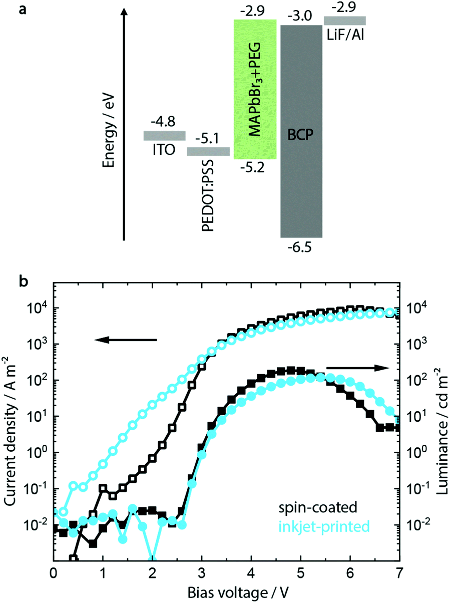 | ||
| Fig. 1 (a) The energy levels of the chosen perovskite light-emitting diode (PeLED) device architecture permit ohmic contact between both the hole and electron injection layer and the semiconducting perovskite. (b) Current density/voltage/luminance characteristics show similar device parameters for the spin-coated and inkjet-printed PeLEDs without KCl as additive. | ||
The resulting devices show a low maximum luminance of 150 to 200 cd m−2 and a typical turn-on voltage Von of 3 V (see Fig. 1b), with devices incorporating inkjet-printed MAPbBr3:PEG layers showing similar parameters to the spin-coated ones. Scanning force microscopy (SFM) and scanning electron microscopy (SEM) images additionally confirm their pinhole-free morphology after fabrication, as shown in Fig. S5 (ESI†).
It has to be noted that particularly the inkjet-printed devices suffer from high leakage current below the turn-on voltage (defined as the applied voltage corresponding to a luminance of 1 cd m−2). SFM and SEM analyses indicate a film of smaller crystallites mixed with singular crystals with a bigger grain size, congruent with the less controlled crystallization process during drying after inkjet printing. In contrast, the spin-coated layer shows a more monodisperse distribution of grain sizes (see Fig. S5, ESI†).
As introduced above, we incorporated the alkali salt KCl into the PEDOT:PSS hole injection layer in order to improve the performance of inkjet-printed as well as spin-coated devices. In the following, we show in detail the morphological and electrical effects this has on both the HIL and the light-emitting perovskite layer. It should be noted that blending the KCl directly into the perovskite solution yields unstable solvent systems due to the poor solubility of KCl in the perovskite solution solvents of DMF/DMSO.53
HIL employing KCl-enriched PEDOT:PSS
When blending KCl into the PEDOT:PSS layer, we encounter only a minor effect on the layer resistivity, consistent with the values of 500 to 5000 Ω cm given by the manufacturer (Heraeus). The resistivity decreased from 978 to 827 Ω cm with increasing KCl concentration to 20 g L−1, as shown in Table 1. This is in line with previous observations that certain salts have only negligible influence on the electrical properties of PEDOT:PSS, depending on the ability of the cation to bind to PSS− chains and thereby influence the resistivity.61,62Secondly, PEDOT:PSS is a well-known hole transport material with a typical work function of around 5.1 eV.63 From photoelectron yield spectroscopy (PYS) measurements, only a minor decrease from 5.1 eV to 4.9 eV is shown when increasing the KCl amount to 20 g L−1, which can be considered as negligible when considering the margin of error of the technique. For the sake of clarity, we will discuss in the following only the incorporation of no salt, low (5 g L−1) and high (15 g L−1) salt concentration on the PEDOT:PSS layer. The full datasets (including 1, 10 and 20 g L−1) can be found in the ESI.†
First of all, we observe a strong influence on the morphology of the PEDOT:PSS layer upon addition of KCl, as shown in the optical microscopy and SFM images reported in Fig. 2a and b for pure PEDOT:PSS layers and with addition of 5 and 15 g L−1 KCl. The additional KCl concentrations are presented in Fig. S7 and S8 (ESI†). PEDOT:PSS layers without added KCl appear featureless in optical microscopy images and SFM images. At the low KCl concentration of 5 g L−1, small crystallites with nm height are visible in the optical microscopy image. At a higher concentration of 15 g L−1, clear dendritic structures are visible, extending over tens of microns and hundreds of nm in height as shown by SFM measurements.
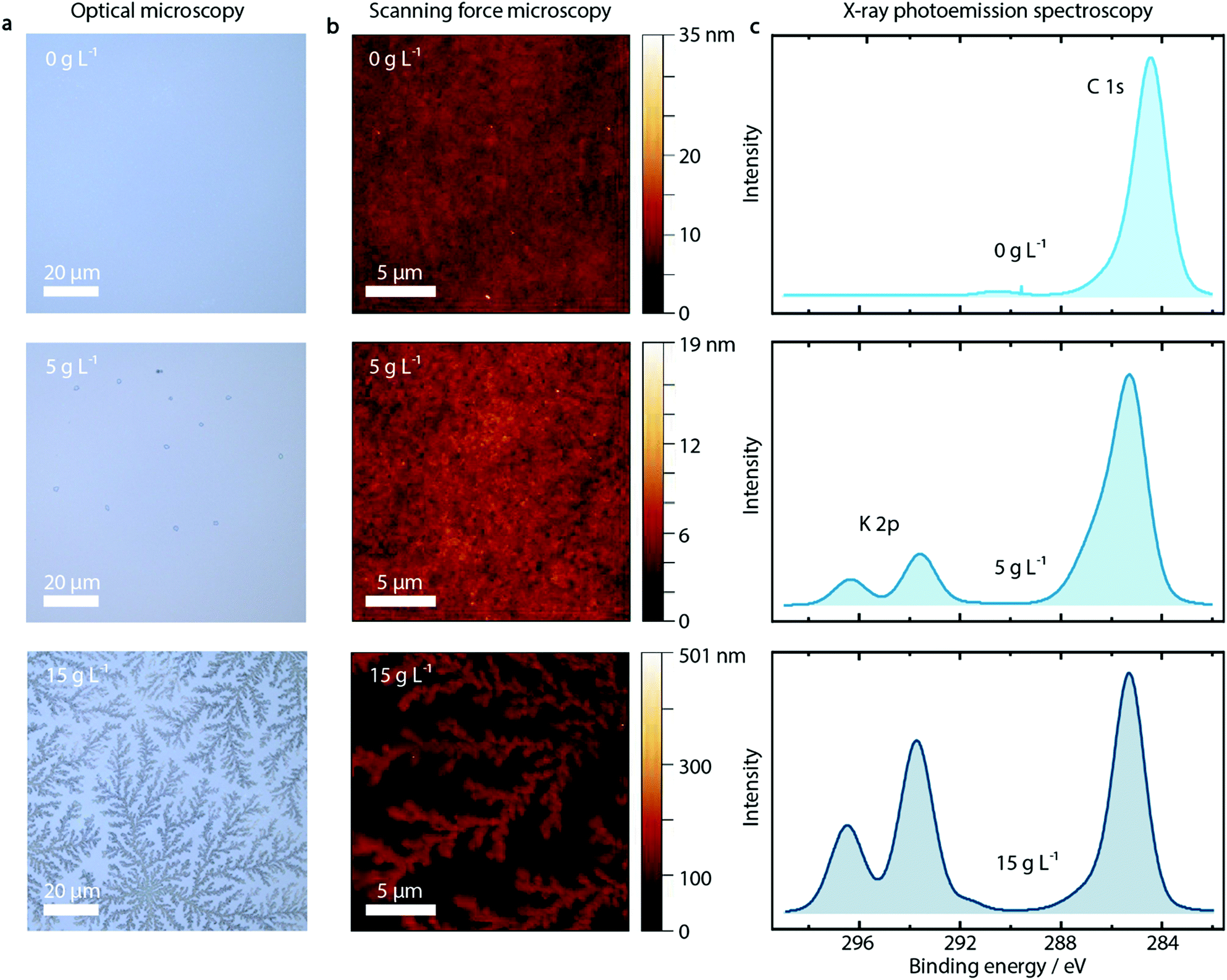 | ||
| Fig. 2 Effect of KCl incorporated within the PEDOT:PSS layers. The optical microscopy (a) and scanning force microscopy images (b) of the PEDOT:PSS films show a clear influence of the concentration of KCl additive (0, 5, 15 g L−1) on the film morphology. XPS spectra (c) indicate that as the KCl concentration increases within the PEDOT:PSS films, so does the K 2p peak (doublet at 295 eV) corresponding to the added KCl. The C 1s peak (285 eV) corresponding to the PEDOT:PSS surface shows no change. | ||
Probing the PEDOT:PSS/KCl surface by X-ray photoemission spectroscopy (XPS), we see increasing potassium K 2p peaks (binding energy 293 eV and 297 eV) with increasing KCl content blended in the PEDOT:PSS layer, as shown in Fig. 2c and in Fig. S9 (ESI†) for the complete series of KCl concentrations. Additionally, when analyzing the relative K+ content as a function of KCl concentration, after an initial linear trend we observe saturation of the K+ content from a concentration of 10 g L−1 (see Fig. S9, ESI†).
Since XPS is an extremely surface-sensitive technique (depth of scan is approximately 3 nm) the presence of K 2p peaks in the spectra, together with the resulting relative K+ content, indicates that KCl is present on the surface of the PEDOT:PSS layer. Even at the lowest concentration of 1 g L−1, the K 2p peaks start to arise (see Fig. S9, ESI†).
Because the salt ions will predominantly lie within the resulting dendritic structures forming in and protruding out of the PEDOT:PSS surface, we investigated the morphological influence of the PEDOT:PSS/KCl blend on the MAPbBr3:PEG composite deposited on top of the HIL, described in the next section.
MAPbBr3:PEG composite on KCl-enriched PEDOT:PSS
As illustrated in Fig. 3, the dendritic structures that were visible within the PEDOT:PSS layer are also visible in the perovskite film in SFM images, indicating a templating effect on the perovskite layer. Both SFM micrographs as well as SEM images show the influence on the morphology of MAPbBr3:PEG deposited on the PEDOT:PSS layer upon inclusion of KCl. Whereas the crystal domain size seems to be unaffected by the KCl addition, especially at high KCl concentrations of 15 g L−1 and above, the dendritic structure of the PEDOT:PSS/KCl layer is visible.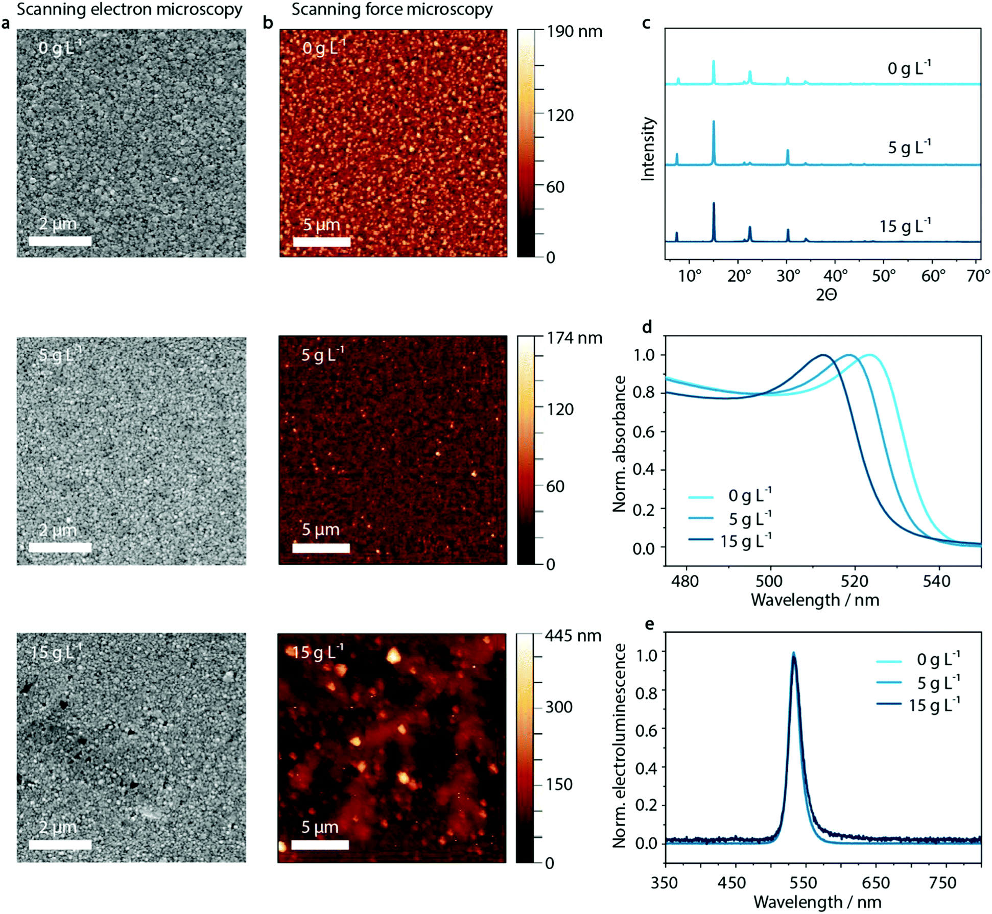 | ||
| Fig. 3 Templating effect of PEDOT:PSS/KCl on the perovskite films. The SEM micrographs (a) and SFM images (b) of MAPbBr3:PEG-composite spin-coated on PEDOT:PSS/KCl show an increasing templating effect when increasing KCl concentration from 0 g L−1 to 5 g L−1 and 15 g L−1. No KCl concentration-dependent changes can be seen in the X-ray diffractograms (c) and electroluminescence spectra (e) of MAPbBr3:PEG-composite fabricated on PEDOT:PSS/KCl, but UV-vis absorption (d) shows a 12 nm shift in absorption onset as a function of KCl content. | ||
In order to investigate the insolubility of these structures in the solvent used for perovskite deposition, the same solvent was spun onto the PEDOT:PSS/KCl layer. As shown in Fig. S10 and Table S1 (ESI†), these washing tests confirm that the dendritic structures are only slightly re-dissolved due to the poor solubility of KCl in the perovskite solvent of DMF/DMSO. The dendritic structures will therefore be able to influence the film formation of the deposited perovskite layer by templating. Additionally, the re-dissolved KCl may induce crystallization of the perovskite within the solution.
Aside from the morphological influence that is shown in the SEM and SFM images, it is necessary to investigate if there is any further diffusion of the K+ or Cl− species from the surface of the PEDOT:PSS layer into the perovskite. X-ray diffraction measurements can provide insight into potential changes in the crystal structure of the perovskite caused by such diffusion. Upon inclusion of K+ or Cl− in the MAPbBr3-lattice, a shift to higher 2θ values would be expected with respect to the XRD peaks of the initial pristine MAPbBr3 phase.64 But, as shown in Fig. 3c and Fig. S11 (ESI†) there is no evidence that either K+ or Cl− ions are incorporated into the perovskite lattice, since the X-ray diffraction patterns show no trend in shifting the corresponding main perovskite reflection at around 15°. (We note that the diffraction peak at 7.5° most likely results from PEG, while 22.5° is PEG overlapping with the 110 lattice plane of MAPbBr3).65
However, when analyzing the UV-vis absorption spectra of the series of perovskite films processed on top of the PEDOT:PSS/KCl films, an influence of additional KCl on the UV-vis absorption can be observed (Fig. 3d). With increasing KCl concentration in the PEDOT:PSS film, the UV-vis absorption edge of the layers measured on PEDOT:PSS/MAPbBr3:PEG shift from 540 nm to 528 nm. This shift by 12 nm is in agreement with an inclusion of below 10% of Cl− with respect to the pure bromide perovskite film. Considering the previously discussed XRD data, this amount should be responsible for a shift in 2θ of less than 0.1°, since the difference in position of the main XRD peak in pristine MAPbBr3 compared to MAPbCl3 is less than 1°.64 But, as noted above, no clear trend in the shift of perovskite reflection at 15° can be seen in the X-ray diffractogram (see Fig. S11, ESI†). We attribute this phenomenon to the measurement method of XRD itself, where changes are only detectable at the macroscopic level which are statistically distributed within the sample. Since the chloride content likely varies considerably throughout the layer, being incorporated from the KCl seed crystals underneath, XRD may not be able to detect such changes.
Despite the change in absorption onset, under electrical operation no effect on the electroluminescence peak position is observed. Independently of the KCl content, a green emission at a wavelength of 530 nm is visible (Fig. 3e). This is an indication of the lower energy bandgap of the pure bromide phase dominating the recombination behavior compared to mixed MAPb(BrxCl1−x)3 perovskite phases – well-known as bias-induced phase segregation.66,67
Having analyzed the effect of including the KCl into PEDOT:PSS on the morphology, crystallization, absorption and electroluminescence behavior, we show the effect on the device performance in spin-coated and inkjet-printed PeLEDs. Inclusion of KCl at a concentration of 5 g L−1 and 15 g L−1 within the PEDOT:PSS layer influences strongly the device performance of PeLEDs based on MAPbBr3:PEG composite active layer. The resulting current density/voltage/luminance (J/V/L) parameters are shown in Fig. 4 and Fig. S12, ESI.†
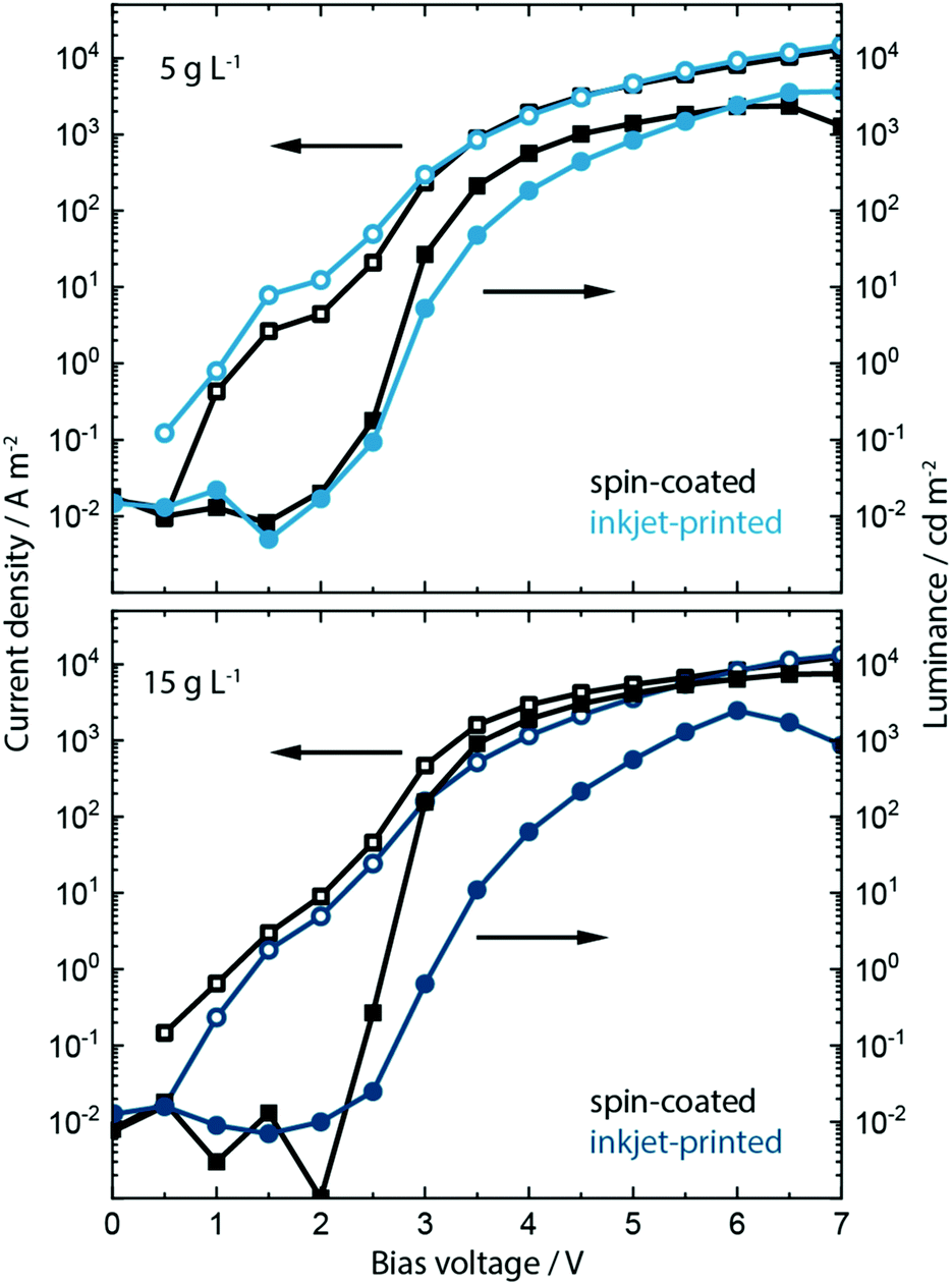 | ||
| Fig. 4 The J/V/L characteristics of PeLEDs fabricated on PEDOT:PSS blended with a low 5 g L−1 KCl content (a) and high 15 g L−1 KCl content (b) indicate the two different optimums depending on the process – for low KCl content devices incorporating the inkjet-printed active layer outperform those incorporating the spin-coated ones. For higher KCl content, it is vice versa. | ||
Recalling the J/V/L parameters of the reference PeLEDs without KCl addition (see Fig. 1), upon inclusion of the low salt concentration of 5 g L−1 both spin-coated as well as inkjet-printed devices now exhibit much higher maximum luminance values of around 2000 and 4000 cd m−2, respectively, and a reduced turn-on voltage Von of around 2.6 V. This is an increase in luminance by a factor of 10 and 20 from the original 200 cd m−2. At the higher bias voltage range of 6 to 7 V, the inkjet-printed PeLEDs therefore outperform the spin-coated ones in current efficacy (cd A−1).
We predominantly trace this efficiency boost back to the templating effect of the PEDOT:PSS/KCl morphology on the perovskite film formation and the resulting grain-size distribution (see Fig. S13 and S14, ESI†). As indicated by the increased luminance values, a rise in electron–hole recombination is occurring. This may be due to more balanced charge carrier transport at the anode, whereby KCl is acting as an additional electron blocking layer. Additionally, smaller grains will lead to greater exciton confinement and increased radiative recombination,42 which is seen in the improved luminance, while non-radiative recombination defects may also be removed from perovskite grain boundaries by passivation through KCl.
Devices incorporating the increased KCl content of 15 g L−1 show a further increase of luminance up to 8000 cd m−2 and a decrease in turn-on voltage to ∼2.5 V for the spin-coated PeLEDs. In contrast, the inkjet-printed PeLEDs show only marginal differences in luminance compared to those containing 5 g L−1 KCl in the PEDOT:PSS layer. We attribute this to the drastically changed morphology (see Fig. S13, ESI†). It is evident that the high KCl amount induces different perovskite crystallization depending on the processing. While the wet perovskite film remains on the PEDOT:PSS/KCl for only a few seconds during spin coating, and this leads to an optimum morphology, the printed perovskite layer rests for 1 to 2 minutes on top of the PEDOT:PSS/KCl layer before crystallization is induced by the post-deposition vacuum step.
In fact, this crystallization behavior is indicative of two different optimums being achieved. Spin-coated MAPbBr3:PEG films form best on top of PEDOT:PSS films incorporating 15 g L−1 of KCl, while for inkjet-printed films this concentration of KCl seems too high. The resulting large dendritic structures within the PEDOT:PSS lead to perovskite crystallites that are too large and yield inhomogeneous films as a consequence. For inkjet-printed MAPbBr3:PEG the best films are achieved when printing on PEDOT:PSS incorporating the lower 5 g L−1 concentration of KCl. Further work aims to understand the influence of any residual KCl within the PEDOT:PSS layer along with the detailed mechanism of crystallization induced by KCl (and alkali salts in general) utilizing optical in situ characterization.68
Conclusions
In summary, for the first time we have produced a light-emitting diode with an inkjet-printed active layer based on MHP perovskite. While there are examples of high-efficiency PeLEDs employing MAPbBr3 reported in literature,43,45 their fabrication was based on non-scalable anti-solvent treatment of the perovskite layer using spin coating. In our work the perovskite layer is instead blended with PEG and processed on top of the salty hole injection layer PEDOT:PSS before being dried under mild vacuum conditions. By incorporating the alkali salt KCl into the HIL, an improvement in the performance parameters of the PeLEDs is achieved. We find evidence that some portion of the KCl in the form of Cl− ions diffuses into the HIL/perovskite interface, resulting in a change in absorption characteristics of the perovskite layer. The emission characteristics, however, are not affected by the KCl, resulting in light emission only of the pure bromide-MAPbBr3:PEG mixture.However, we attribute the performance increase primarily to a change in induced crystallization in the perovskite layer, templated by the underlying KCl structures and resulting morphological influence within the PEDOT:PSS. Furthermore, we find two optimum concentrations of KCl to use within the PEDOT:PSS, depending on the subsequent processing of the perovskite by either spin coating (high KCl concentration allowed) or inkjet printing (low KCl concentration preferred). By using the low KCl concentration, it was possible to produce inkjet-printed PeLEDs showing a high luminance of 4000 cd m−2 and low turn-on voltage, comparable to spin-coated devices. With the passing of this milestone, further work can develop inkjet-printed PeLEDs with different colors and designs, especially for display and other industrial applications.
Experimental
Perovskite solution
Lead bromide (PbBr2) was dissolved in a mixture of DMF and DMSO (7![[thin space (1/6-em)]](https://www.rsc.org/images/entities/char_2009.gif) :3) and shaken at 30 °C for one hour to yield a 0.4 M (147 g L−1, 12 wt%) solution. The clear solution was added to an equimolar amount of MABr powder to yield the 0.4 M (192 g L−1, 15 wt%) MAPbBr3 precursor solution. Polyethylene glycol (PEG) (Mw 6000) was dissolved in a mixture of DMF and DMSO (7:3) and heated to 60 °C until fully dissolved. MAPbBr3 precursor solution was mixed with PEG solution in 2:1 v/v ratio to yield the MAPbBr3:PEG precursor solution. If not noted otherwise, a 50 g L−1 PEG solution was used. The optimized mixture contains 11 wt% perovskite precursor and 1.5 wt% PEG.
:3) and shaken at 30 °C for one hour to yield a 0.4 M (147 g L−1, 12 wt%) solution. The clear solution was added to an equimolar amount of MABr powder to yield the 0.4 M (192 g L−1, 15 wt%) MAPbBr3 precursor solution. Polyethylene glycol (PEG) (Mw 6000) was dissolved in a mixture of DMF and DMSO (7:3) and heated to 60 °C until fully dissolved. MAPbBr3 precursor solution was mixed with PEG solution in 2:1 v/v ratio to yield the MAPbBr3:PEG precursor solution. If not noted otherwise, a 50 g L−1 PEG solution was used. The optimized mixture contains 11 wt% perovskite precursor and 1.5 wt% PEG.
Device fabrication
ITO coated and patterned glass substrates (Psiotec Ltd) were cleaned in an ultrasonic bath using a 2 vol% Mucasol solution, acetone and isopropanol for ten minutes each. The substrates were transferred to a laminar flow box, dried in nitrogen flow and treated for 15 minutes in a UV-ozone cleaner (1 bar oxygen). PEDOT:PSS solution (Al4083 purchased from Heraeus) was filtered with a 0.45 μm nylon filter. The substrates were thoroughly cleaned of any particles in nitrogen flow and then covered with PEDOT:PSS solution and spin-coated at 1500 rpm for 12 seconds and 4000 rpm for 30 seconds, followed by annealing at 220 °C for 10 minutes under a laminar flow hood. PEDOT:PSS/KCl solution were prepared by adding certain amounts of KCl (1 to 20 g L−1) to the PEDOT:PSS dispersion. Spin coating parameters were used as mentioned above. The resulting film had a thickness of 50 nm, as verified by profilometry (Bruker Dektak).Subsequently, 8 nm BCP, 1 nm LiF and 100 nm aluminum were evaporated at a chamber base pressure of 10−6 mbar. The active area had a size of 0.04 cm2. The devices were encapsulated using a commercially available resin (Bluefixx) and hardened with a blue LED in 2 seconds. Measurements took place in ambient atmosphere directly after fabrication.
Thin film characterization
Energy levels of the perovskite layers were determined with ultraviolet photoemission spectroscopy (UPS) using the hydrogen Lyman α line as excitation source, controlled by an Excitech E-lux EPU unit within a Jeol JPS 9030 photoelectron spectrometer. All samples were electrically grounded. Photoelectron yield spectroscopy (PYS) was performed in air with a RIKEN KEIKI AC-2E photoelectron spectrometer to evaluate the work function of PEDOT:PSS. X-ray photoelectron spectroscopy (XPS) measurements were performed on a Jeol JPS 9030 photoelectron spectrometer. The Al K-α line was used for excitation with a monochromator. A path energy of 50 eV was used. All samples were electrically grounded. X-ray diffraction (XRD) measurements were done with a Bruker D8 Advanced XRD machine using a copper K-α source in Bragg–Brentano geometry. Scanning electron microscopy (SEM) images were recorded with a Hitachi S-4100 and 5 kV acceleration voltage system. Microscopy images were acquired with an Olympus SZX16 stereo microscope for images in millimeter range and an Olympus confocal laser microscope (LEXT OLS4100) for images in micrometer range. Scanning force microscopy (SFM) images were taken with a Bruker Dimension Icon SFM machine in tapping mode. SFM data were evaluated using open source software (Gwyddion). Sheet resistance was measured with a Jandel Unit RM3000 four point probe setup with a multiheight probe. Absorption measurements were performed on a PerkinElmer Lambda 950 UV/VIS Spectrometer, whereby transmission was measured and absorption was calculated accordingly.Optoelectronic characterization
Current density/voltage/luminance characteristics were obtained using a 2612B Keithley source meter unit for applied voltage and measured current coupled with an LS 160 luminance meter (Konica Minolta) in a custom setup. Electroluminescence spectra were obtained with an HR 2000+ Ocean Optics spectrometer.Conflicts of interest
There are no conflicts to declare.Acknowledgements
This work was carried out in the framework of the Joint Lab GEN_FAB and with the support of the Helmholtz Innovation Lab HySPRINT. The authors gratefully acknowledge Carola Klimm for SEM measurements and Giovanni Ligorio for critical reading of the manuscript. The authors would also like to thank Norbert Koch for granting instrument access. F. M., C. R. and E. L. U. acknowledge funding from the German Ministry of Education and Research (BMBF) for the Young Investigator Group Hybrid Materials Formation and Scaling (HyPerFORME) within the program “NanoMatFutur” (grant no. 03XP0091), as well as the Helmholtz Energy Materials Foundry (HEMF) and PEROSEED (ZT-0024) project.References
- D. B. Mitzi, Progress in Inorganic Chemistry, 1999, vol. 48, pp. 1–121 Search PubMed.
- S. D. Stranks, G. E. Eperon, G. Grancini, C. Menelaou, M. J. P. Alcocer, T. Leijtens, L. M. Herz, A. Petrozza and H. J. Snaith, Science, 2013, 342, 341–344 CrossRef CAS PubMed.
- A. Kojima, K. Teshima, Y. Shirai and T. Miyasaka, J. Am. Chem. Soc., 2009, 131, 6050–6051 CrossRef CAS PubMed.
- T. S. Kao, Y. H. Chou, C. H. Chou, F. C. Chen and T. C. Lu, Appl. Phys. Lett., 2014, 105, 231108 CrossRef.
- O. A. Jaramillo-Quintero, R. S. Sánchez, M. Rincón and I. Mora-Sero, J. Phys. Chem. Lett., 2015, 6, 1883–1890 CrossRef CAS PubMed.
- B. R. Sutherland and E. H. Sargent, Nat. Photonics, 2016, 10, 295–302 CrossRef CAS.
- Z.-K. Tan, R. S. Moghaddam, M. L. Lai, P. Docampo, R. Higler, F. Deschler, M. Price, A. Sadhanala, L. M. Pazos, D. Credgington, F. Hanusch, T. Bein, H. J. Snaith and R. H. Friend, Nat. Nanotechnol., 2014, 9, 687–692 CrossRef CAS PubMed.
- P. Brenner, M. Stulz, D. Kapp, T. Abzieher, U. W. Paetzold, A. Quintilla, I. A. Howard, H. Kalt and U. Lemmer, Appl. Phys. Lett., 2016, 109, 141106 CrossRef.
- L. Dou, Y. M. Yang, J. You, Z. Hong, W.-H. Chang, G. Li and Y. Yang, Nat. Commun., 2014, 5, 5404 CrossRef CAS PubMed.
- Y. Liu, F. Li, C. P. Veeramalai, W. Chen, T. Guo, C. Wu and T. W. Kim, ACS Appl. Mater. Interfaces, 2017, 9, 11662–11668 CrossRef CAS PubMed.
- J. Liu, B. Shabbir, C. Wang, T. Wan, Q. Ou, P. Yu, A. Tadich, X. Jiao, D. Chu, D. Qi, D. Li, R. Kan, Y. Huang, Y. Dong, J. Jasieniak, Y. Zhang and Q. Bao, Adv. Mater., 2019, 31, 1901644 CrossRef PubMed.
- M. D. Birowosuto, D. Cortecchia, W. Drozdowski, K. Brylew, W. Lachmanski, A. Bruno and C. Soci, Sci. Rep., 2016, 6, 37254 CrossRef CAS PubMed.
- V. B. Mykhaylyk, H. Kraus and M. Saliba, Mater. Horiz., 2019, 6, 1740–1747 RSC.
- C. R. Kagan, Science, 1999, 286, 945–947 CrossRef CAS PubMed.
- D. B. Mitzi, C. D. Dimitrakopoulos and L. L. Kosbar, Chem. Mater., 2001, 13, 3728–3740 CrossRef CAS.
- K. Tanaka, T. Takahashi, T. Kondo, K. Umeda, K. Ema, T. Umebayashi, K. Asai, K. Uchida and N. Miura, Jpn. J. Appl. Phys., 2005, 44, 5923–5932 CrossRef CAS.
- G. Xing, N. Mathews, S. S. Lim, N. Yantara, X. Liu, D. Sabba, M. Grätzel, S. Mhaisalkar and T. C. Sum, Nat. Mater., 2014, 13, 476–480 CrossRef CAS PubMed.
- J. H. Heo, S. H. Im, J. H. Noh, T. N. Mandal, C.-S. Lim, J. A. Chang, Y. H. Lee, H. Kim, A. Sarkar, K. NazeeruddinMd, M. Gratzel and S. Il Seok, Nat. Photonics, 2013, 7, 486–491 CrossRef CAS.
- J. C. Yu, J. H. Park, S. Y. Lee and M. H. Song, Nanoscale, 2019, 11, 1505–1514 RSC.
- S. T. Ha, R. Su, J. Xing, Q. Zhang and Q. Xiong, Chem. Sci., 2017, 8, 2522–2536 RSC.
- C. L. Tai, W. L. Hong, Y. T. Kuo, C. Y. Chang, M. C. Niu, M. Karupathevar Ponnusamythevar Ochathevar, C. L. Hsu, S. F. Horng and Y. C. Chao, ACS Appl. Mater. Interfaces, 2019, 11, 30176–30184 CrossRef CAS PubMed.
- Y. Altintas, I. Torun, A. F. Yazici, E. Beskazak, T. Erdem, M. Serdar Onses and E. Mutlugun, Chem. Eng. J., 2020, 380, 122493 CrossRef CAS.
- M. Era, S. Morimoto, T. Tsutsui and S. Saito, Appl. Phys. Lett., 1994, 65, 676–678 CrossRef CAS.
- T. Hattori, T. Taira, M. Era, T. Tsutsui and S. Saito, Chem. Phys. Lett., 1996, 254, 103–108 CrossRef CAS.
- K. Chondroudis and D. B. Mitzi, Chem. Mater., 1999, 11, 3028–3030 CrossRef CAS.
- K. Sim, T. Jun, J. Bang, H. Kamioka, J. Kim, H. Hiramatsu and H. Hosono, Appl. Phys. Rev., 2019, 6, 031402 Search PubMed.
- Q. Wang, J. Ren, X. F. Peng, X. X. Ji and X. H. Yang, ACS Appl. Mater. Interfaces, 2017, 9, 29901–29906 CrossRef CAS PubMed.
- B. Xu, W. Wang, X. Zhang, W. Cao, D. Wu, S. Liu, H. Dai, S. Chen, K. Wang and X. Sun, J. Mater. Chem. C, 2017, 5, 6123–6128 RSC.
- C. Zou, C. Y. Huang, E. M. Sanehira, J. M. Luther and L. Y. Lin, Nanotechnology, 2017, 28, 455201 CrossRef PubMed.
- T. M. Eggenhuisen, Y. Galagan, A. F. K. V. Biezemans, T. M. W. L. Slaats, W. P. Voorthuijzen, S. Kommeren, S. Shanmugam, J. P. Teunissen, A. Hadipour, W. J. H. Verhees, S. C. Veenstra, M. J. J. Coenen, J. Gilot, R. Andriessen and W. A. Groen, J. Mater. Chem. A, 2015, 3, 7255–7262 RSC.
- F. Mathies, T. Abzieher, A. Hochstuhl, K. Glaser, A. Colsmann, U. W. Paetzold, G. Hernandez-Sosa, U. Lemmer and A. Quintilla, J. Mater. Chem. A, 2016, 4, 19207–19213 RSC.
- F. Mathies, H. Eggers, B. S. Richards, G. Hernandez-Sosa, U. Lemmer and U. W. Paetzold, ACS Appl. Energy Mater., 2018, 1, 1834–1839 CrossRef CAS.
- F. Mathies, E. J. W. List-Kratochvil and E. L. Unger, Energy Technol., 2019, 1900991 Search PubMed.
- M. J. J. Coenen, T. M. W. L. Slaats, T. M. Eggenhuisen and P. Groen, Thin Solid Films, 2015, 583, 194–200 CrossRef CAS.
- T. Shimoda, K. Morii, S. Seki and H. Kiguchi, MRS Bull., 2003, 28, 821–827 CrossRef CAS.
- F. Mathies, P. Brenner, G. Hernandez-Sosa, I. A. Howard, U. W. Paetzold and U. Lemmer, Opt. Express, 2018, 26, A144 CrossRef CAS PubMed.
- I. M. Hossain, D. Hudry, F. Mathies, T. Abzieher, S. Moghadamzadeh, D. Rueda-Delgado, F. Schackmar, M. Bruns, R. Andriessen, T. Aernouts, F. Di Giacomo, U. Lemmer, B. S. Richards, U. W. Paetzold and A. Hadipour, ACS Appl. Energy Mater., 2019, 2, 47–58 CrossRef CAS.
- F. Hermerschmidt, S. A. Choulis and E. J. W. List-Kratochvil, Adv. Mater. Technol., 2019, 4, 1–16 Search PubMed.
- F. Hermerschmidt, I. Burgués-Ceballos, A. Savva, E. D. Sepos, A. Lange, C. Boeffel, S. Nau, E. J. W. List-Kratochvil and S. A. Choulis, Flexible Printed Electron., 2016, 1, 035004 CrossRef.
- R. Eckstein, N. Strobel, T. Rödlmeier, K. Glaser, U. Lemmer and G. Hernandez-Sosa, Adv. Opt. Mater., 2018, 6, 1701108 CrossRef.
- N. J. Jeon, J. H. Noh, Y. C. Kim, W. S. Yang, S. Ryu and S. Il Seok, Nat. Mater., 2014, 13, 897–903 CrossRef CAS PubMed.
- H. Cho, S. H. Jeong, M. H. Park, Y. H. Kim, C. Wolf, C. L. Lee, J. H. Heo, A. Sadhanala, N. S. Myoung, S. Yoo, S. H. Im, R. H. Friend and T. W. Lee, Science, 2015, 350, 1222–1225 CrossRef CAS PubMed.
- S. Lee, J. H. Park, Y. S. Nam, B. R. Lee, B. Zhao, D. Di Nuzzo, E. D. Jung, H. Jeon, J. Y. Kim, H. Y. Jeong, R. H. Friend and M. H. Song, ACS Nano, 2018, 12, 3417–3423 CrossRef CAS PubMed.
- Y. K. Chih, J. C. Wang, R. T. Yang, C. C. Liu, Y. C. Chang, Y. S. Fu, W. C. Lai, P. Chen, T. C. Wen, Y. C. Huang, C. S. Tsao and T. F. Guo, Adv. Mater., 2016, 28, 8687–8694 CrossRef CAS PubMed.
- N. F. Jamaludin, N. Yantara, Y. F. Ng, A. Bruno, B. K. Chandran, X. Y. Chin, K. Thirumal, N. Mathews, C. Soci and S. Mhaisalkar, J. Mater. Chem. C, 2018, 6, 2295–2302 RSC.
- J. Li, S. G. R. Bade, X. Shan and Z. Yu, Adv. Mater., 2015, 27, 5196–5202 CrossRef CAS PubMed.
- L. Song, X. Guo, Y. Hu, Y. Lv, J. Lin, Z. Liu, Y. Fan and X. Liu, J. Phys. Chem. Lett., 2017, 8, 4148–4154 CrossRef CAS PubMed.
- Z. Tang, T. Bessho, F. Awai, T. Kinoshita, M. M. Maitani, R. Jono, T. N. Murakami, H. Wang, T. Kubo, S. Uchida and H. Segawa, Sci. Rep., 2017, 7, 1–7 CrossRef PubMed.
- D. J. Kubicki, D. Prochowicz, A. Hofstetter, S. M. Zakeeruddin, M. Grätzel and L. Emsley, J. Am. Chem. Soc., 2017, 139, 14173–14180 CrossRef CAS PubMed.
- M. Muzammal uz Zaman, M. Imran, A. Saleem, A. H. Kamboh, M. Arshad, N. A. Khan and P. Akhter, Phys. B, 2017, 522, 57–65 CrossRef CAS.
- M. Abdi-Jalebi, Z. Andaji-Garmaroudi, S. Cacovich, C. Stavrakas, B. Philippe, J. M. Richter, M. Alsari, E. P. Booker, E. M. Hutter, A. J. Pearson, S. Lilliu, T. J. Savenije, H. Rensmo, G. Divitini, C. Ducati, R. H. Friend and S. D. Stranks, Nature, 2018, 555, 497–501 CrossRef CAS PubMed.
- M. Abdi-Jalebi, M. I. Dar, A. Sadhanala, S. P. Senanayak, M. Franckevičius, N. Arora, Y. Hu, M. K. Nazeeruddin, S. M. Zakeeruddin, M. Grätzel and R. H. Friend, Adv. Energy Mater., 2016, 6, 1502472 CrossRef.
- J. Dagar, K. Hirselandt, A. Merdasa, A. Czudek, R. Munir, F. Zu, N. Koch, T. Dittrich and E. L. Unger, Sol. RRL, 2019, 3, 1900088 CrossRef.
- P. Wang, J. Wang, X. Zhang, H. Wang, X. Cui, S. Yuan, H. Lu, L. Tu, Y. Zhan and L. Zheng, J. Mater. Chem. A, 2018, 6, 15853–15858 RSC.
- X. Liu, Y. Zhang, L. Shi, Z. Liu, J. Huang, J. S. Yun, Y. Zeng, A. Pu, K. Sun, Z. Hameiri, J. A. Stride, J. Seidel, M. A. Green and X. Hao, Adv. Energy Mater., 2018, 8, 1–12 Search PubMed.
- P. Zhu, S. Gu, X. Luo, Y. Gao, S. Li, J. Zhu and H. Tan, Adv. Energy Mater., 2020, 10, 1903083 CrossRef CAS.
- K. M. Boopathi, M. Ramesh, T.-Y. Huang, W. Budiawan, M. Y. Lin, C.-H. Lee, K.-C. Ho and C. W. Chu, J. Mater. Chem. A, 2016, 4, 1591–1597 RSC.
- R. Munir, A. D. Sheikh, M. Abdelsamie, H. Hu, L. Yu, K. Zhao, T. Kim, O. El Tall, R. Li, D.-M. Smilgies and A. Amassian, Adv. Mater., 2017, 29, 1604113 CrossRef PubMed.
- K. Yan, M. Long, T. Zhang, Z. Wei, H. Chen, S. Yang and J. Xu, J. Am. Chem. Soc., 2015, 137, 4460–4468 CrossRef CAS PubMed.
- S. J. Yoon, K. G. Stamplecoskie and P. V. Kamat, J. Phys. Chem. Lett., 2016, 7, 1368–1373 CrossRef CAS PubMed.
- Y. Xia and J. Ouyang, Macromolecules, 2009, 42, 4141–4147 CrossRef CAS.
- Y. Xia and J. Ouyang, Org. Electron., 2012, 13, 1785–1792 CrossRef CAS.
- N. Koch, A. Vollmer and A. Elschner, Appl. Phys. Lett., 2007, 90, 10–13 CrossRef.
- A. Buin, R. Comin, J. Xu, A. H. Ip and E. H. Sargent, Chem. Mater., 2015, 27, 4405–4412 CrossRef CAS.
- L. C. Chen, K. L. Lee, C. Y. Huang, J. C. Lin and Z. L. Tseng, Micromachines, 2018, 9, 3–10 Search PubMed.
- P. Vashishtha and J. E. Halpert, Chem. Mater., 2017, 29, 5965–5973 CrossRef CAS.
- Y. Zou, Z. Yuan, S. Bai, F. Gao and B. Sun, Mater. Today Nano, 2019, 5, 100028 CrossRef.
- A. Merdasa, C. Rehermann, K. Hirselandt, J. L. Li, O. Maus, J. Dagar, M. Munir and E. L. Unger, submitted.
Footnotes |
| † Electronic supplementary information (ESI) available. See DOI: 10.1039/d0mh00512f |
| ‡ These authors contributed equally to this work. |
| This journal is © The Royal Society of Chemistry 2020 |