
 Open Access Article
 This Open Access Article is licensed under a
 Creative Commons Attribution 3.0 Unported Licence
The damaging effects of the acidity in PEDOT:PSS on semiconductor device performance and solutions based on non-acidic alternatives
Joseph
Cameron
 * and
Peter J.
Skabara
*
* and
Peter J.
Skabara
*
WestCHEM, School of Chemistry, University of Glasgow, Joseph Black Building, University Place, Glasgow, G12 8QQ, UK. E-mail: joseph.cameron@glasgow.ac.uk; peter.skabara@glasgow.ac.uk
First published on 24th March 2020
Abstract
Poly(3,4-ethylenedioxythiophene):poly(styrene sulfonate), PEDOT:PSS, has been widely used as an effective hole transporting material in many different organic semiconductor devices for well over a decade. However, despite having many strong features which make this material such a popular hole transport/injection layer, PEDOT:PSS is well-known to cause degradation in devices and limit their stability due to the acidity of the PSS chain. This review focusses on the attempts that have been made to combat this problem, with different strategies explored, including the development of neutral analogues, use of alternative materials and the introduction of barrier layers to prevent degradation of the electrode. Since solution-processing is a key advantage of using PEDOT:PSS, we concentrate on analogous materials that can also be solution-processed, with particular attention on whether orthogonal processing can be retained. We intend this work to be a useful guide for researchers considering enhanced device lifetimes, an important parameter when considering organic semiconductor devices for commercialisation.
1. Introduction
Poly(3,4-ethylenedioxythiophene):poly(styrene sulfonate) (PEDOT:PSS, Fig. 1), is widely used in organic electronic devices, such as organic photovoltaics (OPVs) and organic light-emitting diodes (OLEDs), whilst also being used in organic–inorganic hybrid devices such as perovskite-based solar cells, as a hole transport layer (HTL). This material is popular due to its high conductivity and transparency, the ability to reduce surface roughness when coating ITO and its suitability for orthogonal processing. Indeed, it can be considered the default hole transport material (HTM) for solution-processed organic semiconductor devices and has been applied successfully in some benchmark OPV1–4 (including the current record PCE device)5 and OLED devices6–8 over the last 10 years. However, there are disadvantages in using PEDOT:PSS, which include acidity, hygroscopicity, anisotropic charge injection9 and batch-to-batch variation in electrical and physical properties. For this reason, there has been much research into developing materials to replace PEDOT:PSS in organic electronic devices.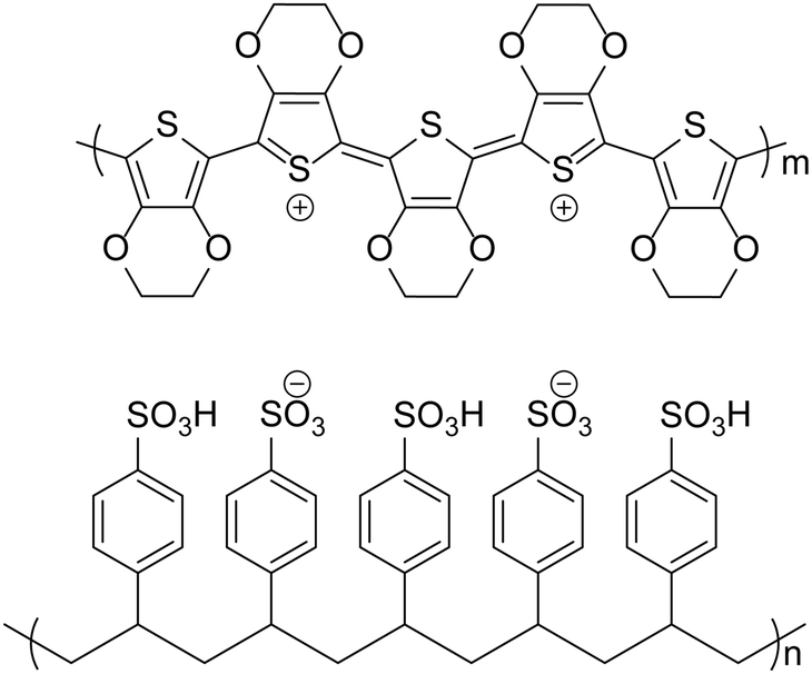 | ||
| Fig. 1 Structure of PEDOT:PSS. | ||
PEDOT:PSS is prepared from the polymerisation of 3,4-ethylenedioxythiophene using an oxidising reagent such as Fe2(SO4)3.10 This leads to the formation of a polymer with a doped backbone, making the polymer conductive, and the conductivity varies with the level of doping. PSS is used to solubilise the monomer and the subsequent polymer in the aqueous solution whilst also balancing the positive charges of the doped PEDOT chains. However, the PSS chains also contain sulfonic acid groups with labile protons causing the solution to be acidic. Nowadays, there are many varieties of PEDOT:PSS available with different formulations, resulting in a range of properties for deposited films. A summary of the properties of some formulations that are often reported in the literature is presented in Table 1.
| PEDOT:PSS formulation | pH | Conductivity (S cm−1) | Work function (eV) |
|---|---|---|---|
| a After the addition of 5% DMSO. | |||
| P VP Al 4083, Clevios™ | 1.0–2.0 (25 °C) | 0.0002–0.002 | 5.2 |
| PH1000, Clevios™ | 1.5–2.5 (25 °C) | ∼0.1–118–20 (850a) | 4.8–5.0 |
| HTL Solar, Clevios™ | 4.0–7.0 (25 °C) | 0.1–1.0 | 4.8–5.0 |
| HTL Solar 3, Clevios™ | Toluene solution | 0.002–0.2 | 4.4–4.8 |
| P Jet N, Clevios™ | 5.0–8.0 | 9–30 | ∼4.7521 |
In this review we will focus on the impact of the acidity of PEDOT:PSS on device performance and stability. Furthermore, we will discuss the steps that can be taken to neutralise PEDOT:PSS or prevent degradation due to acidity. The discussion will be mainly concentrated on alternative HTLs, where the materials possess a stabilised ionisation energy and high p-type mobility or hole injection layers (HILs), where often a thin layer is deposited on the anode to modify the work function and improve hole injection. As solution-processing is one of the main advantages of using PEDOT:PSS, this article presents analogues or alternatives that can be solution-processed. If one is looking for a review on how to enhance the conductivity of PEDOT:PSS then this has been nicely summarised by Xu et al.,11 whilst a comprehensive overview of transparent electrode materials in general can be found in a recent article by Cloutet et al.12 Many of the approaches taken to enhance the conductivity of PEDOT:PSS involve treatment with acids such as formic acid,13 sulfuric acid,14 phosphoric acid15 or the addition of high boiling point solvents, such as DMSO16 or NMP.17 The strong acidity of high conductivity grades of PEDOT:PSS could be problematic for stability or limit the choice of compatible active materials, yet as these developments are relatively recent the literature has not reported these obvious concerns.
There are a number of materials used as transparent conductive electrodes but many of these are susceptible to acid-induced degradation. One of the most commonly used transparent electrodes is indium doped tin oxide (ITO). It has been established that the acidity of PEDOT:PSS causes degradation of the ITO anode. Using Rutherford backscattering spectrometry, de Voigt et al. detected a significant indium content in PEDOT:PSS films after casting, which increased over time with both thermal annealing and exposure to air.22 Therefore, despite the advantages of acidity in boosting conductivity, there is a need, particularly for applications incorporating an HTL, for non-acidic conductive materials to improve device lifetime.
Whilst ITO is widely used in organic electronics, alternative materials have also been explored, particularly due to the low abundance of indium. However, these technologies are also vulnerable to acid-induced degradation. It should be noted that there has also been a report that PEDOT:PSS has not been detrimental to the stability of silver nanowires.23 Understanding the exact nature of degradation in other metals/electrodes is therefore of key importance for the development of organic semiconductor devices based on PEDOT:PSS and its analogues.
The acidity of PEDOT:PSS as a hole transport material can have a detrimental consequence on device performance due to its effect on materials coated on top of it. In 2003, Brunner and co-workers24 studied poly(p-phenylenevinylene) (PPV, Fig. 2) and poly(2,7-spirofluorene) polymer films and the interface with PEDOT:PSS. For the PPV/PEDOT:PSS bilayer, it was observed that photoluminescence quenching occurred as a result of charge carrier-filled defect states. This effect was not present in the poly(2,7-spirofluorene)/PEDOT:PSS interface and the type of cathode material had no role in the formation of defect states. The authors therefore concluded that defect states were created by electrophilic addition of the protons from the PEDOT:PSS to the vinylene bond of the PPV. Degradation of LED performance has also been observed for iridium-based complexes as Baranoff et al.25 showed a blue phosphorescent iridium complex (Firpic, Fig. 2) degrading in the presence of PEDOT:PSS, highlighting that ligand stability can be affected by acidity.25 The acidic nature of PEDOT:PSS has also been shown to be detrimental to some donor materials for OPV devices. Bazan et al.1 noted that pyridyl[2,1,3]thiadiazole (PT) in p-DTS(PTTh2)2 (Fig. 2), is protonated in the presence of PEDOT:PSS and this results in reduced performance, particularly for the open-circuit voltage (VOC). It is therefore important to consider the effects of acid on active layer materials in addition to corrosion of electrodes.
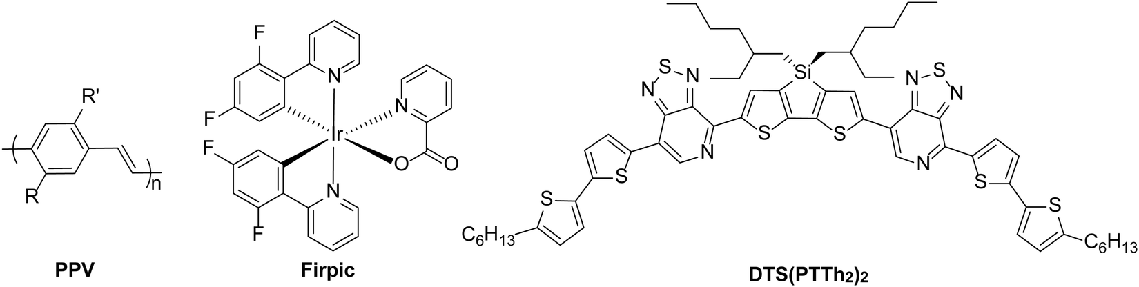 | ||
| Fig. 2 Examples of active materials which have been reported to be sensitive to acid.1,24,25 | ||
The degradation in the performance of organic semiconductor devices can be extremely difficult to monitor due to the fact there are multiple layers and many competing processes. Most organic electronic devices are sensitive to degradation by exposure to air and moisture. Krebs et al.26 were able to demonstrate phase segregation of PEDOT and PSS chains over time with exposure to oxygen and moisture. In inverted devices this leads to selective oxidation of the PEDOT chains and, subsequently, the layers underneath. Also, in constructing OPV devices based on MDMO-PPV:PC61BM as the active layer with and without a PEDOT:PSS layer, Durrant et al.27 were able to use a series of different environmental conditions to show that PEDOT:PSS absorbed water from a humid nitrogen atmosphere causing increased resistivity.
Such observations should be considered as part of the overall understanding of the PEDOT:PSS-assisted degradation mechanism. Indeed, it is likely that a combination of the hygroscopic nature and the acidity of the PSS group leads to breakdown of device performance over time. However, this review will discuss the specific problems that have affected device performance due to acidity and how these challenges can be overcome. Many of the examples discussed show that a simple substitution of an acidic PEDOT:PSS layer for a non-acidic analogue can result in improved device stability. In summarising the different approaches that can be pursued, it is hoped that this review can be a useful source for researchers looking to avoid acid-induced degradation of semiconductor devices.
2. Barrier layers to prevent electrode degradation
A number of different strategies have been used to avoid diffusion of indium from ITO into active layers of organic semiconductor devices. One common tactic to avoid this degradation is to separate the interface between ITO and PEDOT:PSS by placing a barrier between the two layers. For example, Wang et al.28 introduced a double layer of PEDOT:PSS, with pH neutral PEDOT:PSS on top of ITO and the regular solution deposited on top of the neutral layer. The indium etching was shown to be reduced by a factor of 6.5 and the device performance was even improved upon.28In another approach, there have been attempts to coat the ITO with a self-assembled monolayer (SAM) to prevent etching and subsequent migration of indium into the hole transport and active layers. In fact, Tai et al.29 showed that even acidic SAMs such as terephthalic acid and derivatives with four and six carboxylic acid groups (Fig. 3), could be placed in the interface between ITO and PEDOT:PSS to suppress the migration of indium. The SAM-modified device only showed a 30% reduction in power conversion efficiency (PCE) over 49 days, whereas the reference device with an ITO/PEDOT:PSS interface showed no device activity after this time. The initial performances of the tested devices were also comparable whether or not SAMs were applied.
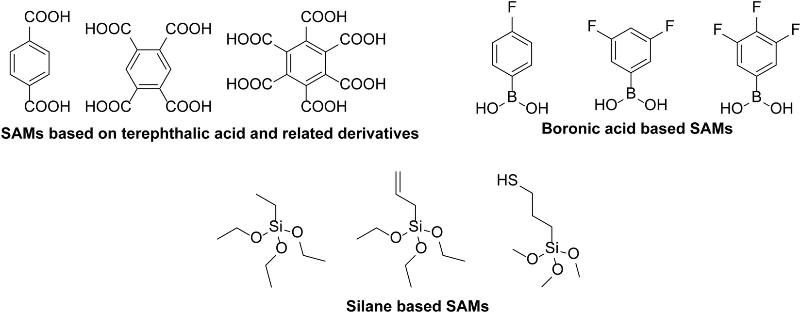 | ||
| Fig. 3 Structures of SAMs used as blocking layers to prevent degradation of ITO from an adjacent PEDOT:PSS layer.29–31 | ||
Lau et al.30 used silane-based SAMs between PEDOT:PSS and ITO which significantly reduced the atomic concentration of indium measured in the PEDOT:PSS layer from 1.7% to 0.04–0.06% for the SAM-modified substrates. One of the SAMs used, allyl-triethoxysilane, produced the best blocking ability, despite giving the lowest thickness when deposited, which was attributed to cross-linking of the C![[double bond, length as m-dash]](https://www.rsc.org/images/entities/char_e001.gif) C bonds upon heating. Kara et al.31 used boronic acid based materials with variable number of fluorine atoms (1F, 2F and 3F; Fig. 3), to form a SAM on the ITO surface. The electron withdrawing nature of the SAMs improved the hole injection between ITO and PEDOT:PSS, resulting in an improvement in the short-circuit current (JSC) of planar perovskite solar cells from 19.48 to 22.20 mA cm−2, and a significant increase in PCE (12.49% to 15.66%), for the 2F SAM. Additionally, devices containing the 2F SAM showed considerably better stability over 30 days with only a 20% reduction in PCE, compared to a 75% reduction in the original PCE of the non-modified device over the same time.
C bonds upon heating. Kara et al.31 used boronic acid based materials with variable number of fluorine atoms (1F, 2F and 3F; Fig. 3), to form a SAM on the ITO surface. The electron withdrawing nature of the SAMs improved the hole injection between ITO and PEDOT:PSS, resulting in an improvement in the short-circuit current (JSC) of planar perovskite solar cells from 19.48 to 22.20 mA cm−2, and a significant increase in PCE (12.49% to 15.66%), for the 2F SAM. Additionally, devices containing the 2F SAM showed considerably better stability over 30 days with only a 20% reduction in PCE, compared to a 75% reduction in the original PCE of the non-modified device over the same time.
There is also an example, presented by Baik et al., of a thin diamond-like carbon layer being used as a buffer layer between ITO and PEDOT:PSS to prevent indium migration to the HTL and EML of OLEDs.32 The carbon-based buffer layer, deposited by sputtering with Ca2+, significantly reduced the indium concentration in the PEDOT:PSS layer (0.004 wt%) compared to the device without a buffering layer (1.2 wt%), as determined by Rutherford backscattering spectrometry. The barrier layer also improved the OLED performance, with devices containing a MEH-PPV emissive layer showing significantly improved current efficiency with addition of the carbon barrier layer. Similarly, graphene oxide has also been used as a barrier between the ITO and PEDOT:PSS interface. Sulaiman et al.33 showed that introducing graphene oxide both increased the PCE of PCDTBT/PC71BM based solar cells (4.28% and 3.57% with and without graphene oxide, respectively), and improved the lifetime of the OPV devices.
Metal oxides are well known to be used as hole injection layers (see section 4.1: Solution-processed metal oxides/metal complexes). However, such materials have also been used in a bilayer with PEDOT:PSS to prevent acid-induced degradation of ITO. For example, Park et al.34 reported using tungsten oxide (WOx) prepared from tungsten and hydrogen peroxide with dilution using isopropanol. OPV devices based on a P3HT:PC61BM active layer were fabricated with PEDOT:PSS, WOx and bilayers of WOx/PEDOT:PSS where the concentration of WOx solution was also varied. There was similar performance in each of the devices although the devices containing PEDOT:PSS showed the highest efficiency. However, the stability of the devices was greatly enhanced when using either WOx or the WOx/PEDOT:PSS bilayer suggesting that either route can be an effective means of reducing instability whilst maintaining performance.
Using a barrier to reduce the etching of ITO and diffusion of indium ions into the PEDOT:PSS layer (and subsequently the active layer), has been shown to be an effective means of improving the stability of different organic electronic devices. However, any acid-sensitive materials in the active layer may also degrade and ultimately reduce performance and/or stability. However, there are many different solution-processable hole transport layers that are non-acidic and can also be used in place of PEDOT:PSS to improve the overall stability.
3. Solution-processable alternative materials to PEDOT:PSS
There are many different approaches that have been taken to replace PEDOT:PSS in organic semiconductor devices. However, PEDOT:PSS has been effectively used for over 10 years to give good device performance and it is generally regarded as the best and most convenient material available for electronic device applications. Films of PEDOT:PSS have a high transparency, low surface roughness, reasonably well-aligned energy levels and moderate-to-high conductivity depending on the formulation. Any alternative materials that are developed must match or improve on these properties, in addition to reducing the acidity, if they are to be viable candidates to replace PEDOT:PSS.3.1 pH neutral PEDOT:PSS solutions
The most intuitive means to mitigate against the degradation of PEDOT:PSS is to use a pH neutral version of the widely-used hole transport material. However, Okuzaki et al. showed that making PEDOT:PSS pH neutral can cause distinct changes in the properties with reduced conductivity, increased absorption in the NIR region and reduced order in the film.35 Additionally, de Kok and co-workers analysed PEDOT:PSS when treated with sodium hydroxide. Typically PEDOT:PSS shows broad absorption in the NIR region which is attributed to bipolarons (Fig. 4), the presence of which increase with increased doping level, and this absorption is reduced significantly when the pH of PEDOT:PSS increases as a result of treatment with NaOH.36 In fact it was shown that the change in absorbance is similar to treatment of PEDOT:PSS with reducing agent hydrazine, which would cause de-doping.36 Therefore neutralisation of PEDOT:PSS destabilises bipolarons in the polymer backbone and effectively reduces the doping level, explaining the reduction in conductivity observed by Okuzaki and co-workers as a result of increasing pH.35 In addition to the conductivity, the reduced doping level as a result of increased pH will be expected to affect the work function of the layer, as Meerholz and co-workers demonstrated that the work function of electrochemically grown PEDOT films could be varied by controlling the doping level.37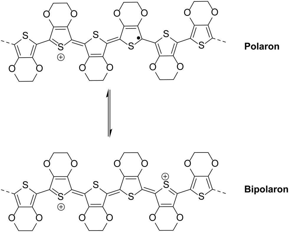 | ||
| Fig. 4 Structures of a polaron and bipolaron formed as a result of doping in the PEDOT backbone. | ||
Therefore, direct replacement often results in a reduction in performance due to differences in formulation. For example, Kim and co-workers38 studied the effect of reacting PEDOT:PSS with NaOH. Increasing the amount of NaOH led to an increase in pH, as expected. However, at NaOH concentrations >0.2 M, device performance was compromised due to a combination of increased resistance, a reduction in the work function (from 5.3 to 4.9 eV) and increased surface roughness. However, the devices formed using the layer deposited from the 0.2 M treated solution showed improved stability compared to devices containing pristine PEDOT:PSS when exposed to light for 10 hours at 100 mW cm−2 (a reduction in PCE to 2.19%, compared to 1.65% for the acidic solution, where initially the devices showed PCEs ∼ 3.5%). This illustrates that reducing the acidity of PSS is an effective means of improving the lifetime, although other challenges arise as a result of treatment with base.
An aqueous guanidine solution was used by Guo et al.39 to modify PEDOT:PSS and the resulting solution had a pH of 7.0–7.5. The films formed using the neutral PEDOT:PSS showed similar transmittance and sheet resistance to the non-modified film (PH1000; Table 1). Interestingly, tests of both PEDOT:PSS films deposited on silver nanowires (AgNWs) showed similar mechanical stability over 1200 bending cycles, with just a small increase in sheet resistance, highlighting how neutralised PEDOT:PSS can be used for flexible electronic devices. The neutral PEDOT:PSS/AgNWs films (and films of only AgNWs), also showed improved stability when exposed to high temperatures and no evidence of degradation under stress testing at a constant applied current. There was a significant decrease in the current of acidic PEDOT:PSS/AgNWs, showing that the acidity led to degradation of the AgNWs.
Similarly, Kim et al.40 reported using imidazole to reduce the acidity of PEDOT:PSS and the resulting solution was deposited onto AgNWs. In this study, the AgNWs showed good stability at room temperature over 36 days, irrespective of whether the PEDOT:PSS used was pH neutral or acidic (PH1000; Table 1). However, at high temperature (85 °C), the sheet resistance of AgNW/acidic PEDOT:PSS severely increased, whilst the increased temperature had little impact on the neutral film (or the AgNWs alone). The authors reasoned that the increased heat led to the solubilisation of Ag in the acidic environment as Ag is insoluble at room temperature in sulfonic acid, but can dissolve with heating. Interestingly, when subjected to hot and humid conditions (85 °C and 85% humidity), degradation occurred at a similar rate in both PEDOT:PSS films, whilst there was degradation of the AgNWs alone too, albeit to a lesser extent. The authors ascribed this degradation process to the formation of hydrogen sulfide (H2S) and carbonyl sulfide (COS).
Wang et al.28 reported that using a commercial neutral PEDOT:PSS solution, Clevios™, Jet N (Table 1), which is sold as a formulation aimed at inkjet printing, gave comparatively poor performance in OLEDs containing a poly[2-(4-(3′,7′-dimethyloctyloxy)-phenyl)-p-phenylenevinylene] (P-PPV) emissive layer, compared to an acidic PEDOT:PSS layer (14![[thin space (1/6-em)]](https://www.rsc.org/images/entities/char_2009.gif) 942 cd m−2vs. 57337 cd m−2 maximum luminance). The non-acidic variant showed reduced indium concentration as determined by XPS (0.02 vs. 0.13%), highlighting that the neutral layer should improve stability. However, the performance of the devices containing the neutral layer could be enhanced by UV plasma treatment, resulting in comparable maximum luminance and current efficiency values to the OLEDs containing acidic HTLs. The authors attributed the improvement to modified energy levels leading to improved hole injection, suggesting this is an effective means of overcoming one of the previously identified challenges of neutralising PSS – reduction in the work function leading to poor hole injection. This strategy was also applied to HTLs in OPV devices containing a PCDTBT/PC71BM active layer where the PCE of the acidic reference device (P VP Al 4083) decreased by 45% over 50 days, whilst there was only a 20% reduction in the PCE of a device containing a neutral PEDOT:PSS (Jet N) layer that was treated twice with UV ozone/O2 plasma.28 The authors reported that the conductivity and work function of a Jet N layer treated only once with O2 plasma are similar to the double-treated layer but the double treatment leads to a reduction in the roughness of the film, consequently improving the performance (6.11% vs. 6.60% PCE).
942 cd m−2vs. 57337 cd m−2 maximum luminance). The non-acidic variant showed reduced indium concentration as determined by XPS (0.02 vs. 0.13%), highlighting that the neutral layer should improve stability. However, the performance of the devices containing the neutral layer could be enhanced by UV plasma treatment, resulting in comparable maximum luminance and current efficiency values to the OLEDs containing acidic HTLs. The authors attributed the improvement to modified energy levels leading to improved hole injection, suggesting this is an effective means of overcoming one of the previously identified challenges of neutralising PSS – reduction in the work function leading to poor hole injection. This strategy was also applied to HTLs in OPV devices containing a PCDTBT/PC71BM active layer where the PCE of the acidic reference device (P VP Al 4083) decreased by 45% over 50 days, whilst there was only a 20% reduction in the PCE of a device containing a neutral PEDOT:PSS (Jet N) layer that was treated twice with UV ozone/O2 plasma.28 The authors reported that the conductivity and work function of a Jet N layer treated only once with O2 plasma are similar to the double-treated layer but the double treatment leads to a reduction in the roughness of the film, consequently improving the performance (6.11% vs. 6.60% PCE).
Zhang et al.41 took a novel approach to creating a neutral PEDOT:PSS solution by combining standard acidic PEDOT:PSS (Clevios™, P VP Al 4083; Table 1) with (NH4)2MoO4 before thermal decomposition to form MoO3in situ. The solution was used to deposit a hole transport layer in a conventional OPV device with TQ1:PC71BM as the active layer, where TQ1 is a quinoxaline-based polymer used as the donor material in this OPV cell. When compared with devices containing PEDOT:PSS (PCE = 5.5%), or solution-processed MoO3 (PCE = 5.4%), the composite film gave the highest PCE (6.4%). The device lifetime studies showed that the device with an acidic PEDOT:PSS layer had no performance after 10 days. The MoO3–PEDOT:PSS composite showed excellent stability compared to the acidic layer with 80% of its PCE retained after 10 days. The degradation of the current was visualised with photocurrent images over time with exposure to ambient conditions (Fig. 5). Surprisingly, the MoO3–PEDOT:PSS composite showed improved stability when compared to solution-processed MoO3 showing that neutralised PEDOT:PSS can demonstrate enhanced stability when compared to pure metal oxide films.
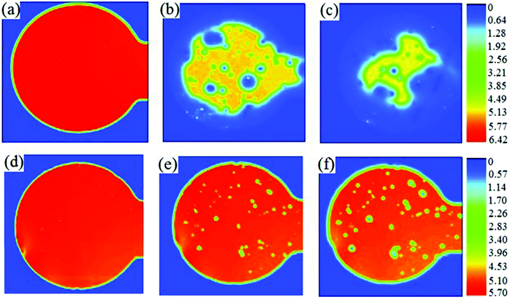 | ||
| Fig. 5 Laser beam induced photocurrent images of the devices exposed to ambient air: (a and d) 0 days; (b and e) 4 days and (c and f) 8 days. The hole-transport layer was PEDOT:PSS (a–c) or MoO3–PEDOT:PSS (d–f). The colour scale represents the photocurrent. Reproduced with permission.41 Copyright 2013, WILEY-VCH Verlag GmbH & Co. KGaA, Weinheim. | ||
The mechanism of degradation was studied in further detail with experiments carried out in humid N2 and dry O2 environments. In a dry O2 atmosphere, the observed degradation of all of the devices was small, even for the OPV with an acidic PEDOT:PSS layer. However, in a humid nitrogen atmosphere (35% humidity), there were clear differences in the extent of degradation for each of the devices. The device with acidic PEDOT:PSS degraded completely after 3 days. The composite film was again significantly better than the solution-processed MoO3-based device which the authors attributed to reduced hygroscopic nature. This emphasises that neutral PEDOT:PSS formulations can outcompete hole transport materials based on metal oxides in both performance and stability.
A common route to improve the efficiency of organic photovoltaics is to fabricate tandem solar cells,42 where two or more cells with different absorption profiles are combined. Where there are more layers introduced, however, solution-processing becomes more challenging. For example, acidic solutions of PEDOT:PSS are problematic for this role as they will dissolve the ZnO layer. Indeed, Moet et al.43 carried out a study where the pH of PEDOT:PSS was modified using aqueous solutions of 2-dimethylaminoethanol. The absorbance of ZnO at 350 nm was monitored with deposition of layers of PEDOT:PSS with varying pH and it was determined that the absorbance of ZnO was significantly reduced at pH < 3. The researchers also observed that the work function of PEDOT:PSS could be reduced with increasing pH by up to approximately 0.7 eV. This would result in poor hole injection for any materials with a relatively stabilised HOMO. However, it was demonstrated that Nafion™ solution could be deposited on top of the neutral PEDOT:PSS to restore the hole injection ability.43
Janssen et al.44 also demonstrated that six layers of a tandem device could be solution-processed, with PEDOT:PSS being used as an intermediate layer to be deposited on top of the electron-transport layer (ZnO) of the first cell. The authors used a neutral dispersion of PEDOT:PSS (Orgacon, batch 5541073, pH = 7. 1.2 wt%, Agfa Gevaert NV), which did not disrupt any of the layers underneath. The resulting solar cell could achieve a high open-circuit voltage of 2.19 V, close to the sum of the VOCs for the separate cells, highlighting the potential for solution-processed tandem OPV devices.
3.2 PEDOT formulations (and analogues) containing different polyelectrolytes
It has been shown that using neutral PEDOT:PSS can be a viable replacement for its acidic analogue in maintaining performance in organic semiconductor devices and improving the stability through treatment of the PSS chain with base. However, it may be possible to take an alternative route and formulate PEDOT with a different polyelectrolyte. This approach has been pioneered by Hadziioannou and co-workers who first reported aqueous PEDOT dispersions with a polystyrene-based polyelectrolyte with (trifluoromethylsulfonyl)imide groups for development of transparent polymer electrodes.45 Although the main focus of this work was on improving the conductivity and processability for application as a transparent electrode, polymer blends with varying pH were synthesised. It was noted that, in a basic solution, the polymerisation rate was slowed, highlighting a challenge of creating non-acidic PEDOT:polyelectrolyte formulations. The work was extended into a comprehensive analysis of PEDOT formulations with many different polyelectrolytes such as polysaccharides and other polystyrenesulfonylimide derivatives with solutions ranging from pH 3.3–8.6 (Fig. 6).46 Although it was concluded that strong acidic groups are required for improved doping, and therefore conductivity, the properties determined for the formulations with the higher pHs suggest potential for these to be used as hole transport layers. As far as we know, such studies investigating the effect of such formulations on device stability compared to PEDOT:PSS have not yet been carried out but this could be a useful future strategy to counteract the degradation by acidic PSS chains in organic semiconductor devices. However, it is important to be mindful of the work function of such a blend and how this will impact on the hole injection of any active layer.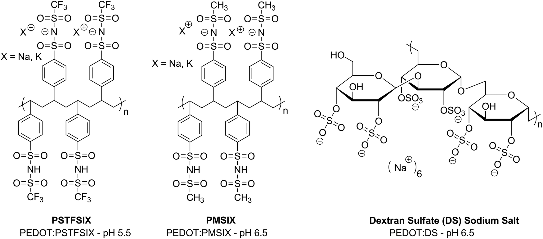 | ||
| Fig. 6 Examples of polyelectrolytes that have been used with PEDOT complexes, reported by Hadziioannou et al.46 | ||
An alternative approach to studying different polyelectrolytes can be to incorporate this functionality into the polymer backbone, as has been achieved in the polymer sulfonated poly(thiophene-3-[2-(2-methoxyethoxy)ethoxy]-2,5-diyl) (P3MEET), originally developed by Plextronics, Inc. (Fig. 7). The polymer was shown to possess properties such as conductivity and transmittance comparable to PEDOT:PSS.47 Although this is an acidic polymer, it is less acidic than PEDOT:PSS due to the reduced number of sulfonate groups. Furthermore, as the polymer is a single component, it does not suffer from the disadvantage of PEDOT:PSS where there can be many insulating PSS-rich domains at the interface.48
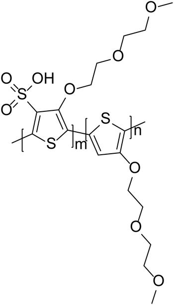 | ||
| Fig. 7 Structure of S-P3MEET developed by Plextronics, Inc. | ||
3.3 Forming PEDOT films in situ
Whilst one strategy to counteract the damaging effects of the acidity of PEDOT:PSS is to formulate PEDOT with a different polyelectrolyte, another consideration is to deposit PEDOT polymer chains without any polyelectrolyte, only corresponding counter ions. This is particularly challenging due to the planar backbone and strong aggregation of PEDOT which makes it poorly soluble in polar and non-polar solvents. However, recently methods have been developed to form a polymer solution in situ or induce solid-state polymerisation of EDOT-based films. The solid-state polymerisation of PEDOT was first reported by Wudl et al.49 Deposition of PEDOT directly from the EDOT monomer has also been reported by Gleason and co-workers using an oxidative chemical vapour deposition.50 This involves EDOT being introduced as a vapour and reacting with a sublimed oxidant such as Fe(III)Cl3.The concept of polymerising an EDOT-based monomer on the substrate was further developed by Patra et al.51 to be compatible with solution-processing. In this study, 2,5-dibromo-3,4-ethylenedioxythiophene was deposited onto ITO substrates by spin-coating from a chlorobenzene solution and the monomer underwent solid-state polymerisation by heating the film overnight at 60 °C. The resulting PEDOT films had a room temperature conductivity of ∼100 S cm−1 and comparable transmittance to PEDOT:PSS. OPV devices fabricated using the polymer HTL with a P3HT/PC61BM active layer only recorded a maximum of 0.71% PCE, whilst PCDTBT/PC71BM-based materials achieved a maximum PCE of 1.70%. The explanation for the reduced efficiencies of these films was the high roughness caused using the solid-state polymerisation approach.
More commonly, PEDOT can be formed in solution with small anionic counter ions and solution-processed without polyelectrolyte species. This method is commonly applied when using PEDOT as an electrode material. In depositing the conducting polymer without the need for the insulating PSS chain, these can achieve high conductivities. However, these solutions are often formulated using strong acids such as sulfuric acid;52 it would be fascinating if such an approach could be adapted in the future to be non-acidic.
4. Alternative HTLs to PEDOT–PSS
4.1 Solution-processed metal oxides/metal complexes
There are several non-acidic hole injection materials that are commonly deposited by vacuum deposition, including MoO3,53,54 WO3,55 V2O556 and CuI57 for example. However, many of these materials are not easily solubilised in common organic solvents for solution-processing. Therefore, additional strategies are necessary if these are to be used for solution-processing. However, due to the attractive properties of metal oxide and metal complexes, including high work function and high transparency, there has been much work into the development of solution-processable metal oxides and metal complexes.Initial methods to deposit metal oxides involved the use of nanoparticles of the materials, but when these were dispersed and deposited as films the roughness could be high due to large aggregates forming.58 However, methods were improved to produce more uniform surfaces. An early example of this was reported in 2011 by Riedl et al.,59 who used vanadium(V) oxotriisopropoxide in an isopropanol solution to deposit layers of V2O5. The resulting films had a low surface roughness (0.4 nm), high work function (5.6 eV in pristine film and 5.3 eV with annealing), and improved both the performance and stability of OPV devices containing a P3HT/PC61BM active layer when compared to a PEDOT:PSS-containing analogue.
In devices where MoO3 is used effectively as a vacuum-deposited hole transport material, molybdenum oxide solutions have been used successfully for solution-processing. One of the first demonstrations of solution-processed MoO3 being effective in maintaining the performance and improving the stability of organic semiconductor devices was from Rand et al., using a sol–gel method.60 This involved dissolving MoO3 in H2O2, refluxing for 2 hours and, once cooled, adjusting the concentration and viscosity using polyethylene glycol and 2-methoxyethanol before spin-coating of films. X-ray photoelectron spectroscopy confirmed the presence of MoO3 after thermal treatment at 350 °C, but the peaks were broader when compared to the evaporated sample due to the presence of several oxidation states (Fig. 8(a)). Nonetheless, when the solution-processed MoO3 was applied to OPV devices containing SubPc/PC61BM and P3HT/PC61BM active layers, the devices gave competitive performance compared to the equivalent PEDOT:PSS containing devices. Furthermore, whilst the inclusion of PEDOT:PSS caused the device to degrade below 20% of its PCE after 200 hours, the solution-processed MoO3 layer could still achieve 70% of its initial PCE after 1000 hours, which was similar to devices containing the evaporated film (Fig. 8(b)).
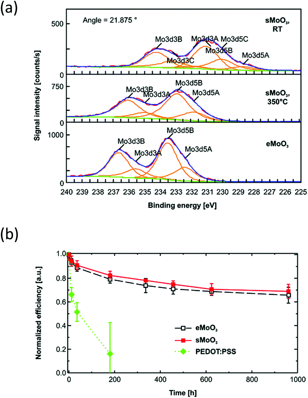 | ||
| Fig. 8 (a) X-Ray photoelectron spectroscopy of solution-processed MoO3 (sMoO3) compared to an evaporated film (eMoO3) and (b) stability of OPV devices with P3HT:PC61BM active layer, stored in ambient conditions reported by Rand et al.60 Reprinted with permission from ref. 60. Copyright 2011 American Chemical Society. | ||
Similarly, Vasilopoulou et al. showed that solution-processed MoO3 and hydrogen molybdenum bronze solutions could be used in OPV devices with a P3HT/PC71BM active layer, giving competitive or better performance with respect to the PEDOT:PSS-containing analogue.61 Additionally, stability studies showed that devices fabricated using molybdenum oxide or hydrogen molybdenum bronze retained more than 80% of the short-circuit current after 800 hours, whilst the device with PEDOT:PSS showed zero current density after only ∼120 hours, illustrating the severity of PEDOT:PSS-induced degradation.61 An alternative means of developing an aqueous solution-processed molybdenum oxide formulation was presented by Li et al. who used (NH4)6Mo7O24·4H2O as a precursor.62 It was used in quantum dot light-emitting diodes (QLEDs), giving superior current efficiency (5.46 vs. 4.49 cd A−1) and comparable maximum luminance, whilst also giving enhanced lifetime and mechanical stability after bend testing at 5 mm radius curvature compared to the analogous device containing PEDOT:PSS.
Tungsten oxide is also a commonly used material for evaporated hole transport layers and can be deposited via solution-processing without the need for hydrogen peroxide, with often a tungsten(VI) alkoxide solution being deposited and annealed in air. For example, Kim et al.63 used tungsten ethoxide in ethanol and stored the films overnight in air to allow formation of WO3 by hydrolysis. They showed higher transmittance than PEDOT:PSS at >580 nm and although the performance is reduced relative to PEDOT:PSS when used in OPV devices containing P3HT:PC61BM (3.77% vs. 3.37%), the layer contributes to significantly improved stability when exposed to air with light soaking. Li et al.64 were able to show that a tungsten oxide layer deposited from tungsten(VI) isopropoxide could improve performance in OPV devices using P3HT:PC61BM and P3HT:IC60BA blends, highlighting that solution-processed WO3 can be used to improve device performance, as well as lifetime, when used in place of PEDOT:PSS.
It has also been shown that nickel oxide-based films can be used as hole transport layers. NiOx can impart an electron blocking ability and improve the energy level alignment between the hole injection layer and the donor polymer.65,66 Olson et al.67 used a solution-processed NiOx layer to improve the performance of a PCDTBT:PC71BM blend (17.3% increase in efficiency). The improvement over PEDOT:PSS-based solar cells was explained by improved selective contact of the work function, which was assisted with oxygen plasma treatment. Additionally, in a test of analogous devices under constant illumination, OPV devices containing the solution-deposited NiOx layer showed a 10-fold improvement in stability when compared to PEDOT:PSS-containing devices.
So and co-workers68 demonstrated that a precursor solution of nickel acetate tetrahydrate and monoethanolamine in ethanol could be deposited for use in OPV devices. The films require heating at 275 °C for conversion to NiO and as a result show improved transmittance compared to PEDOT:PSS above 600 nm, at regions where there is greater overlap with the solar spectrum. The OPV devices showed improvement in efficiency when compared to PEDOT:PSS (7.8% vs. 6.8%), although the authors demonstrated how critical the heating step of the NiO precursor film was – heating at temperatures of 185 °C or 230 °C severely reduced the performance as the film is not conductive if there is not sufficient thermolysis. The main improvement in performance was determined to be as a result of improved uniformity and surface energy of the NiO film when compared to PEDOT:PSS. Finally, it was shown that the NiO layer caused a significant improvement in stability of the OPV device, highlighting another advantage of using such a layer in place of PEDOT:PSS. A further demonstration of the wide scope of NiOx was reported by Choy and co-workers in the form of NiOx nanoparticles, which could be formed by dissolving Ni(NO3)2·6H2O in deionised H2O, adjusting the pH of the solution to 10 using NaOH, filtering and drying the resulting solid before being calcined at 270 °C and dispersed in deionised H2O for processing.69 This dispersion could be used to improve the performance of OPV devices with PCDTBT:PC71BM, PTB7:PC71BM and PTB7-Th:PC71BM active layers and also in an OLED containing a P-PPV emissive layer.
As well as metal oxides, other metal complexes can be used and copper complexes such as CuSCN, for example, have been shown to be an effective hole injection layer. Anthopoulos and co-workers had previously determined that thin films of CuSCN deposited from solution could exhibit high p-type mobility in thin film transistors (TFTs) up to 0.1 cm2 V−1 s−1.70,71 Building on this observation, Anthopoulos et al.72 used CuSCN in 3 types of OPV devices based on P3HT:ICBA, p-DTS(FBTTh2)2:PC71BM and PDPP-2T-TT:PC71BM blends. These were compared with reference devices where PEDOT:PSS had been used in place of CuSCN. Devices with the copper-based HIL showed strong performance in all devices, bettering the PCE of reference PEDOT:PSS-containing devices with P3HT:ICBA and PDPP-2T-TT:PC71BM active layers, whilst showing similar performance in the DTS(FBTTh2)2:PC71BM-based OPV compared to the literature value of a PEDOT:PSS containing device (6.89% vs. 7.0%1). Where the CuSCN devices were directly compared to a PEDOT:PSS reference device, it was clear that an increased short-circuit current was the cause of the improved performance. Indeed, the authors showed that CuSCN shows high transmittance between 360–1400 nm (Fig. 9), whereas PEDOT:PSS absorbs in the visible and NIR regions. The external quantum efficiency plots showed improved efficiency across the visible region and NIR regions, confirming that reduced parasitic absorption of the HTL is the main mechanism for improvement in the OPV devices when CuSCN is used in place of PEDOT:PSS. The fact it was demonstrated that this layer could be universally applied to improve OPV performance makes CuSCN a promising candidate for replacing PEDOT:PSS.
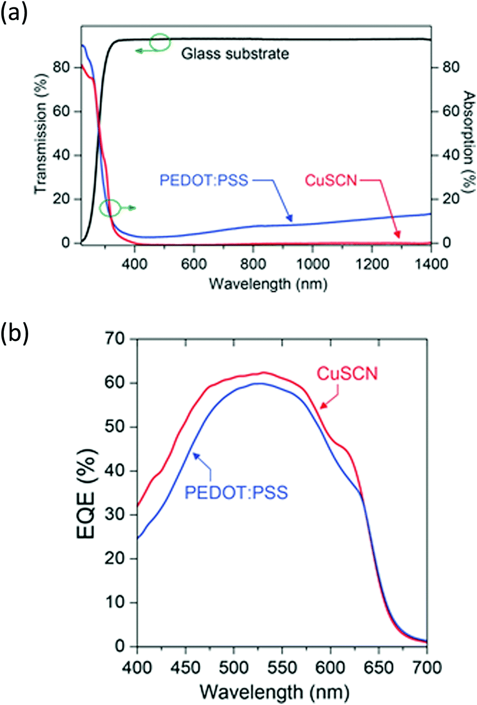 | ||
| Fig. 9 (a) Transmittance of CuSCN compared to PEDOT:PSS (top), and (b) EQE plots for P3HT:ICBA-based OPV devices containing the two hole transport layers.72 Reproduced with permission.72 Copyright 2015, WILEY-VCH Verlag GmbH & Co. KGaA, Weinheim. | ||
Bradley et al.73 reported using CuSCN as a HTL/HIL that could be solution-processed from diethyl sulfide in place of PEDOT:PSS. The resulting (ppy)2Ir(acac)-based OLEDs showed improved efficiency and turn-on voltage when CuSCN was used. Moreover, a TEM image of the device cross-section showed that the interface between the CuSCN layer and the EML was sharp and well-defined, showing that the layer was compatible with orthogonal processing of chlorobenzene solutions. One of the drawbacks of the CuSCN layer, however, was that there was efficiency roll-off after ∼1000 cd m−2 and at between 2000–3000 cd m−2 the PEDOT:PSS-containing device was more efficient. The poorer efficiency resilience of the CuSCN device was attributed to the nature of the layer – it is a semiconductor with relatively low mobility, whereas PEDOT:PSS is a doped conductor. However, Sun and co-workers74 showed, in studies using CuSCN in CdSe@ZnS core–shell-based QLED devices, that when compared to the analogous PEDOT:PSS-containing device, the maximum current efficiency could again be higher when using CuSCN as HIL but the efficiency roll-off was similar to the PEDOT:PSS device.
Copper(I) iodide can also be used as a hole transport layer. Wei et al.75 chose to use CuI as a hole transport material in an inverted perovskite solar cell (PSC) due to its high transparency, good stability under ambient conditions and low cost. The CuI could be deposited from an acetonitrile solution. The resulting PSCs showed a slight improvement in efficiency when compared to devices with a PEDOT:PSS layer but there was a remarkable difference in stability. After 14 days storage in air the PEDOT:PSS containing device retained only 27% of its efficiency, whilst the CuI analogue maintained 90% of its initial PCE.
There are many metal complexes that have been developed to be easily solution-processed for organic semiconductor devices. Often they have advantages of improved transmittance and an increased work function to improve hole injection. Therefore, such materials should be considered as viable alternatives to PEDOT:PSS with a proven ability to reduce acid-induced degradation of devices.
4.2 Solution-processed graphene oxide and transition metal dichalcogenides
The discovery of graphene in 200476 has prompted much interest in the use of 2D-materials for many applications, including water filtration,77 transparent conductive electrodes,78 field-effect transistors79 and photocatalytic water splitting80 for example. Whilst the high conductivity of graphene lends itself to applications such as electrodes due to its high conductivity,81 2D semiconductors such as transition metal dichalcogenides or insulating graphene oxide can be used in organic semiconductor devices. A summary of 2D materials being used in solution-processed solar cells can be found in recent review articles by Kymakis et al.82 and Kim et al.83These 2D materials have been used in place of PEDOT:PSS with beneficial properties resulting. Solution-processed graphene oxide was used by Chhowalla and co-workers in place of PEDOT:PSS in OPV devices with P3HT/PC61BM active layer.84 Due to the insulating nature of graphene oxide, the layer thickness was critical to performance. A 2 nm thick layer in the OPV device resulted in a PCE (3.5%) that was comparable with the PEDOT:PSS reference device (3.6%), but the 4 nm and 10 nm layers caused significant reduction in performance. Hersam and co-workers used graphene oxide deposited by Langmuir–Blodgett assembly followed by treatment with UV-ozone to tune the graphene oxide ionisation energy with the HOMO of the donor polymer used (PTB7).85 The resulting OPV devices with PTB7:PC71BM active layer showed extremely similar performance irrespective of whether PEDOT:PSS (PCE = 7.46%) or graphene oxide (PCE = 7.39%) was used. However, there was a noticeable difference in lifetime between devices when exposed to thermal treatment and humidity lifetime studies. Heating encapsulated devices at 80 °C in an N2 atmosphere caused a small reduction in efficiency for the graphene oxide based devices (∼90% original PCE) with a slightly larger performance reduction for the PEDOT:PSS containing cells (∼83% original PCE). When 80% humidity studies were carried out on devices with air-stable electrodes (TiO2/Ag), the PEDOT:PSS layer caused almost complete degradation in performance after 6 hours whilst the cell with the graphene oxide layer retained >80% of its original PCE. This illustrates the potential for such interlayers to improve the stability of solar cells and other organic semiconductor devices.
Transition metal dichalcogenides are another class of materials which have shown promise when used in place of PEDOT:PSS in organic semiconductor devices. Often synthesis/deposition of such layers has required harsh or energy-intensive processing, but formulations have been developed for solution-processed layer deposition.
Kim and co-workers reported that metal sulfides, WS2 and MoS2, could be spin-coated from precursor solutions of (NH4)WS4 and (NH4)MoS4, respectively, and used as hole transport layers in OLED and OPV devices.86 However, the precursor films required treatment by chemical vapour deposition with H2 and N2 gases used, and a later step requiring hydrogen fluoride etching, demonstrating that the processing is complicated for such hole transport layers compared to PEDOT:PSS for example. Nonetheless, the MoS2 and WS2 layers caused significant improvement in the lifetime of P3HT/PC61BM based OPV devices, with the original PCE values only slightly lower than that reported for the PEDOT:PSS reference device. A different approach can involve using lithium intercalation and exfoliation method, as reported by Li and co-workers.87 The resulting MoS2 and WS2 films were used in perovskite solar cells and showed superior performance when compared to PEDOT:PSS-based devices. When stored in ambient conditions, the PCE of the PEDOT:PSS containing device almost degraded completely after 35 days but devices containing MoS2 and WS2 showed 78% and 72% of their average PCEs, respectively, after 56 days, highlighting the greater stability that can be achieved by using transition metal dichalcogenide layers.87 There is a drawback from the lithium intercalation and exfoliation method though, which requires stirring of bulk MoS2/WS2 in n-butyllithium, which is pyrophoric.
Exfoliation of WS2 layers, however, can be carried out using relatively benign procedures. For example, Anthopoulos and co-workers presented sonication-assisted exfoliation in 1:1 ethanol/deionised water solutions followed by centrifugation. The nanosheet suspensions could be spin-coated onto ITO and when applied to OPV devices (PBDB-T 2F:Y6:PC71BM active layer), the device with a WS2 hole transport layer gave a maximum PCE of 17.0% compared to 16.4% for a PEDOT:PSS containing device. The improvement was attributed to reduced series resistance (RS) and an increase in fill factor and short-circuit current, emphasising the potential for using WS2 hole transporting layers in organic semiconductor devices.
4.3 Organic hole transport layers for solution processing
There are many organic HTLs that are commonly used in evaporated OLEDs or OPV devices, for example. However, these materials are often incompatible for solution-processed devices – either they are too soluble in common solvents used to deposit active layers of organic semiconductor devices, making interlayer mixing a problem, or have poor solubility in most solvents due to their molecular design. Materials such as spiro-OMeTAD are commonly used in perovskite solar cells and can be deposited on top of the perovskite layer. These materials have been discussed in recent review articles.88,89 However, the processability of such materials is limited – depositing organic solutions on top of a layer of spiro-OMeTAD would be challenging due to dissolution and interlayer mixing when solutions of common solvents are used. Therefore, the discussion is focussed on materials with solution-processing properties typically more appropriate for the majority of organic semiconductor devices. Such organic materials should either be polar in nature to allow orthogonal processing or have the ability to be insolubilised after deposition, by cross-linking for example. Additionally, we have focussed on examples where the materials have been compared directly to PEDOT:PSS reference devices in terms of performance and lifetime (Fig. 10).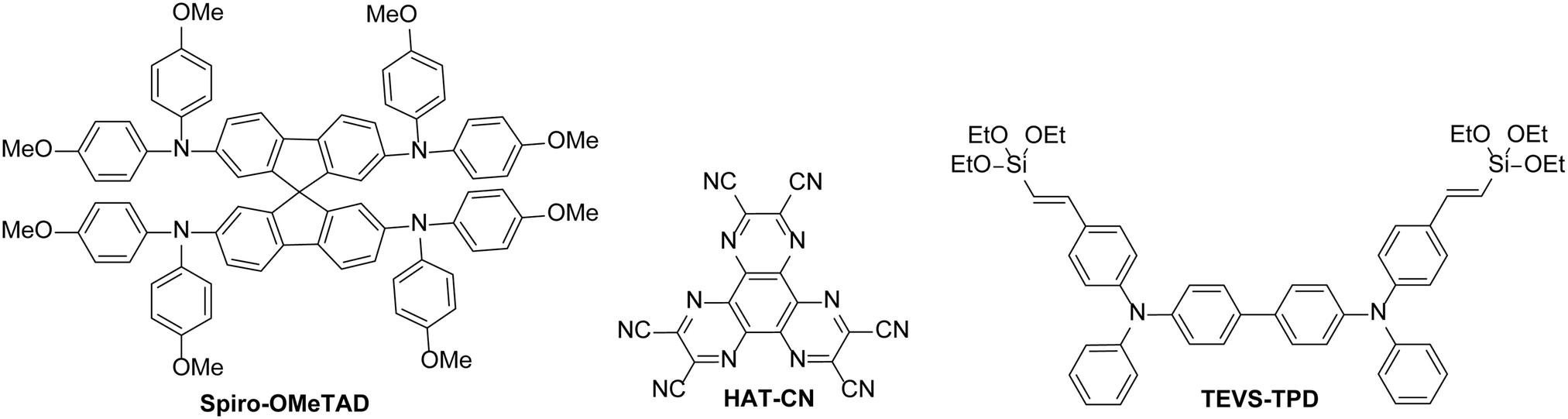 | ||
| Fig. 10 Examples of organic materials used as hole transport layers. | ||
In 2011, Yoon and co-workers90 reported a cross-linkable material based on the small molecule N,N,N′,N′-tetraphenyl-1,1′-biphenyl-4,4′-diamine (TPD), known to have good hole mobility and commonly used in evaporated OLEDs. The molecule was modified to include triethoxysilylvinyl groups which could be thermally cross-linked by curing at 180 °C for 1 hour. When applied to OLEDs based on a PVK/IrPPy3 emissive layer, the cross-linked TPD-based polymer showed a higher maximum luminance and almost identical efficiencies to the analogous device which had a PEDOT:PSS hole injection layer. When the polymer was deposited on top of PEDOT:PSS to be used as a hole transport layer, the performance was reduced, highlighting that the cross-linked polymer is most effective when used in place of PEDOT:PSS.
The choice of material for the hole injection layer is not only limited to molecules based on electron-rich donor materials. Lin et al. showed that a thin layer of the electron-deficient 1,4,5,8,9,11-hexaazatriphenylene hexacarbonitrile (HAT-CN) could be used in place of PEDOT:PSS.91 It could be processed using acetone and the resulting layer was insoluble in many common organic solvents used for the deposition of active materials, including toluene and chlorobenzene. The scope of using this material as a HIL was tested with the fabrication of devices based on Firpic (Fig. 2), Ir(mppy)3 and Os(btfp)2(pp2b) emissive materials and VB-FNPD, a thermally cross-linkable host containing fluorene and triaryldiamine units. The devices with a HAT-CN layer either outperformed or gave consistent performance compared to equivalent devices with PEDOT:PSS layers, illustrating the potential of this material to be used effectively in place of PEDOT:PSS. The thin layer was found to improve charge injection from the anode, with the electron-deficient nature of HAT-CN allowing electron transfer between the HIL and the host in a similar manner as if the host was p-doped using HAT-CN.91
Conventional perovskite solar cells often contain organic materials such as spiro-OMeTAD as hole transport materials deposited on top of the perovskite layer. The perovskite structure is more compatible for orthogonal processing and therefore there are many organic materials soluble in common organic solvents that can be used effectively. There is also great interest in inverted perovskite solar cells due to their ability to suppress the hysteresis effect known to trouble perovskite solar cells.92 However, inverted PSCs have challenges, of which one is the poor surface coverage of the perovskite film on metal oxide hole transport layers, therefore alternatives to metal oxides and PEDOT:PSS must be sought. Heeger et al.93 showed the use of CPE-K (Fig. 11), a conjugated polyelectrolyte, as an HTM in place of PEDOT:PSS, despite most conjugated polyelectrolytes being used as electron transport layers. UV/Vis absorption confirmed that the perovskite film could be deposited without dissolution of the CPE-K layer. The CPE-K and reference layers showed similar surface roughness and PEDOT:PSS exhibited improved transmittance. However, the PSC fabricated using the conjugated polyelectrolyte showed improved performance over the reference device (12.51% vs. 10.77%). Despite the transmittance being lower for CPE-K, PSCs containing this layer demonstrated a higher EQE for most of the visible spectrum compared to the analogous device. The overall improved EQE was attributed to differences in the absorption and interference effect of the two HTLs. The authors carried out a degradation study in air and observed that the perovskite film deposited onto PEDOT:PSS changed from brown to yellow in colour over time, whilst the CPE-K based films did not show any significant changes. In terms of performance, the PCE was reduced by 99% in the PEDOT:PSS-based device after 35 minutes and the device containing the conjugated polyelectrolyte showed clear improved stability with only 55% reduction in PCE. The same polyelectrolyte had also previously been shown to improve the performance of OPV devices fabricated using PTB7:PC71BM and p-DTS(FBTTh2)2:PC71BM active layers when compared to cells with PEDOT:PSS, showing that CPE-K has the potential be used effectively in many different solar cells or other organic semiconductor devices.94
 | ||
| Fig. 11 Structure of polyelectrolyte CPE-K. | ||
Depositing organic materials to be used as hole transport/injection materials is inherently more difficult than processing metal oxides, for example, due to the typical non-polar nature of these materials. However, insolubilising layers via cross-linking can be an effective means of solution-processing a layer with post-processing treatment making it compatible for device fabrication. Furthermore, there are examples of organic materials that can be processed in polar solvents and are resistant to dissolution with typical organic solvents such as toluene and chlorobenzene. Such materials have the potential to be used in place of PEDOT:PSS in the future, particularly for the development of flexible electronic devices.
5. Conclusions
In this review article we have highlighted many of the challenges and complications that can arise when using acidic solutions of PEDOT:PSS, particularly for device stability. However, many of these problems can be overcome by using several different strategies, including the use of solution-processed metal oxides, barrier layers and pH neutral PEDOT:PSS for example. Therefore, it is possible to improve device lifetime and performance by using one of these approaches. The choice of replacement for PEDOT:PSS will depend on properties such as energy level alignment, hole mobility or even stability to flexibility. Often, one of the main advantages quoted for organic semiconductors when used as the active material in organic electronics devices is that they are tuneable and easily modified. The wide range of potential replacements for PEDOT:PSS highlighted in this article demonstrates that there is huge scope to improve the stability of a wide range of different organic electronic devices containing different organic active layers.Conflicts of interest
There are no conflicts of interest to declare.Acknowledgements
The authors thank the EPSRC for funding under grants EP/P02744X/2 and EP/N035496/2.References
- T. S. van der Poll, J. A. Love, T.-Q. Nguyen and G. C. Bazan, Adv. Mater., 2012, 24, 3646–3649 CrossRef CAS.
- L. Nian, K. Gao, Y. Jiang, Q. Rong, X. Hu, D. Yuan, F. Liu, X. Peng, T. P. Russell and G. Zhou, Adv. Mater., 2017, 29, 1700616 CrossRef PubMed.
- Q. Zhang, B. Kan, F. Liu, G. Long, X. Wan, X. Chen, Y. Zuo, W. Ni, H. Zhang, M. Li, Z. Hu, F. Huang, Y. Cao, Z. Liang, M. Zhang, T. P. Russell and Y. Chen, Nat. Photonics, 2014, 9, 35–41 CrossRef.
- L. Meng, Y. Zhang, X. Wan, C. Li, X. Zhang, Y. Wang, X. Ke, Z. Xiao, L. Ding, R. Xia, H.-L. Yip, Y. Cao and Y. Chen, Science, 2018, 361, 1094–1098 CrossRef CAS PubMed.
- Q. Liu, Y. Jiang, K. Jin, J. Qin, J. Xu, W. Li, J. Xiong, J. Liu, Z. Xiao, K. Sun, S. Yang, X. Zhang and L. Ding, Sci. Bull., 2020, 65, 272–275 CrossRef.
- X. Yang, H. Guo, B. Liu, J. Zhao, G. Zhou, Z. Wu and W.-Y. Wong, Adv. Sci., 2018, 5, 1701067 CrossRef PubMed.
- T.-H. Han, M.-R. Choi, C.-W. Jeon, Y.-H. Kim, S.-K. Kwon and T.-W. Lee, Sci. Adv., 2016, 2, e1601428 CrossRef PubMed.
- S. Y. Lee, T. Yasuda, H. Komiyama, J. Lee and C. Adachi, Adv. Mater., 2016, 28, 4019–4024 CrossRef CAS PubMed.
- C. Ionescu-Zanetti, A. Mechler, S. A. Carter and R. Lal, Adv. Mater., 2004, 16, 385–389 CrossRef CAS.
- F. Louwet, L. Groenendaal, J. Dhaen, J. Manca, J. Van Luppen, E. Verdonck and L. Leenders, Synth. Met., 2003, 135–136, 115–117 CrossRef CAS.
- H. Shi, C. Liu, Q. Jiang and J. Xu, Adv. Electron. Mater., 2015, 1, 1500017 CrossRef.
- A. I. Hofmann, E. Cloutet and G. Hadziioannou, Adv. Electron. Mater., 2018, 4, 1700412 CrossRef.
- D. A. Mengistie, M. A. Ibrahem, P.-c. Wang and C.-w. Chu, ACS Appl. Mater. Interfaces, 2014, 6, 1–6 CrossRef PubMed.
- L. Bießmann, N. Saxena, N. Hohn, M. A. Hossain, J. G. C. Veinot and P. Müller-Buschbaum, Adv. Electron. Mater., 2019, 5, 1800654 CrossRef.
- W. Meng, R. Ge, Z. Li, J. Tong, T. Liu, Q. Zhao, S. Xiong, F. Jiang, L. Mao and Y. Zhou, ACS Appl. Mater. Interfaces, 2015, 7, 14089–14094 CrossRef CAS PubMed.
- J. Liu, X. Wang, D. Li, N. E. Coates, R. A. Segalman and D. G. Cahill, Macromolecules, 2015, 48, 585–591 CrossRef CAS.
- C.-h. Chen, J. C. LaRue, R. D. Nelson, L. Kulinsky and M. J. Madou, J. Appl. Polym. Sci., 2012, 125, 3134–3141 CrossRef CAS.
- Y. Xia and J. Ouyang, ACS Appl. Mater. Interfaces, 2012, 4, 4131–4140 CrossRef CAS PubMed.
- T.-R. Chou, S.-H. Chen, Y.-T. Chiang, Y.-T. Lin and C.-Y. Chao, J. Mater. Chem. C, 2015, 3, 3760–3766 RSC.
- K. Lim, S. Jung, S. Lee, J. Heo, J. Park, J.-W. Kang, Y.-C. Kang and D.-G. Kim, Org. Electron., 2014, 15, 1849–1855 CrossRef CAS.
- Y. Meng, Z. Hu, N. Ai, Z. Jiang, J. Wang, J. Peng and Y. Cao, ACS Appl. Mater. Interfaces, 2014, 6, 5122–5129 CrossRef CAS PubMed.
- M. P. de Jong, L. J. van Ijzendoorn and M. J. a. de Voigt, Appl. Phys. Lett., 2000, 77, 2255–2257 CrossRef CAS.
- W.-Y. Jin, R. T. Ginting, K.-J. Ko and J.-W. Kang, Sci. Rep., 2016, 6, 36475 CrossRef CAS PubMed.
- A. van Dijken, A. Perro, E. A. Meulenkamp and K. Brunner, Org. Electron., 2003, 4, 131–141 CrossRef CAS.
- E. Baranoff, B. F. E. Curchod, J. Frey, R. Scopelliti, F. Kessler, I. Tavernelli, U. Rothlisberger, M. Grätzel and M. K. Nazeeruddin, Inorg. Chem., 2012, 51, 215–224 CrossRef CAS PubMed.
- K. Norrman, M. V. Madsen, S. A. Gevorgyan and F. C. Krebs, J. Am. Chem. Soc., 2010, 132, 16883–16892 CrossRef CAS PubMed.
- K. Kawano, R. Pacios, D. Poplavskyy, J. Nelson, D. D. C. Bradley and J. R. Durrant, Sol. Energy Mater. Sol. Cells, 2006, 90, 3520–3530 CrossRef CAS.
- S. Wu, S. Han, Y. Zheng, H. Zheng, N. Liu, L. Wang, Y. Cao and J. Wang, Org. Electron., 2011, 12, 504–508 CrossRef CAS.
- M.-C. Chen, Y.-S. Chiou, J.-M. Chiu, A. Tedla and Y. Tai, J. Mater. Chem. A, 2013, 1, 3680–3687 RSC.
- K. W. Wong, H. L. Yip, Y. Luo, K. Y. Wong, W. M. Lau, K. H. Low, H. F. Chow, Z. Q. Gao, W. L. Yeung and C. C. Chang, Appl. Phys. Lett., 2002, 80, 2788–2790 CrossRef CAS.
- D. Akın Kara, K. Kara, G. Oylumluoglu, M. Z. Yigit, M. Can, J. J. Kim, E. K. Burnett, D. L. Gonzalez Arellano, S. Buyukcelebi, F. Ozel, O. Usluer, A. L. Briseno and M. Kus, ACS Appl. Mater. Interfaces, 2018, 10, 30000–30007 CrossRef PubMed.
- S. H. Choi, S. M. Jeong, W. H. Koo, S. J. Jo, H. K. Baik, S.-J. Lee, K. M. Song and D. W. Han, Thin Solid Films, 2005, 483, 351–357 CrossRef CAS.
- S. Rafique, S. M. Abdullah, M. M. Shahid, M. O. Ansari and K. Sulaiman, Sci. Rep., 2017, 7, 39555 CrossRef CAS PubMed.
- W. Kim, J. Kyu Kim, Y. Lim, I. Park, Y. Suk Choi and J. Hyeok Park, Sol. Energy Mater. Sol. Cells, 2014, 122, 24–30 CrossRef CAS.
- Y. Mochizuki, T. Horii and H. Okuzaki, Trans. Mater. Res. Soc. Jpn., 2012, 37, 307–310 CrossRef CAS.
- M. M. de Kok, M. Buechel, S. I. E. Vulto, P. van de Weijer, E. A. Meulenkamp, S. H. P. M. de Winter, A. J. G. Mank, H. J. M. Vorstenbosch, C. H. L. Weijtens and V. van Elsbergen, Phys. Status Solidi A, 2004, 201, 1342–1359 CrossRef CAS.
- H. Frohne, D. C. Müller and K. Meerholz, ChemPhysChem, 2002, 3, 707–711 CrossRef CAS PubMed.
- H. Kim, S. Nam, H. Lee, S. Woo, C.-S. Ha, M. Ree and Y. Kim, J. Phys. Chem. C, 2011, 115, 13502–13510 CrossRef CAS.
- S. Chen, L. Song, Z. Tao, X. Shao, Y. Huang, Q. Cui and X. Guo, Org. Electron., 2014, 15, 3654–3659 CrossRef CAS.
- S. Kim, S. Y. Kim, M. H. Chung, J. Kim and J. H. Kim, J. Mater. Chem. C, 2015, 3, 5859–5868 RSC.
- S. Shao, J. Liu, J. Bergqvist, S. Shi, C. Veit, U. Würfel, Z. Xie and F. Zhang, Adv. Energy Mater., 2013, 3, 349–355 CrossRef CAS.
- T. Ameri, N. Li and C. J. Brabec, Energy Environ. Sci., 2013, 6, 2390–2413 RSC.
- D. J. D. Moet, P. d. Bruyn and P. W. M. Blom, Appl. Phys. Lett., 2010, 96, 153504 CrossRef.
- J. Gilot, M. M. Wienk and R. A. J. Janssen, Appl. Phys. Lett., 2007, 90, 143512 CrossRef.
- A. I. Hofmann, W. T. T. Smaal, M. Mumtaz, D. Katsigiannopoulos, C. Brochon, F. Schütze, O. R. Hild, E. Cloutet and G. Hadziioannou, Angew. Chem., Int. Ed., 2015, 54, 8506–8510 CrossRef CAS PubMed.
- A. I. Hofmann, D. Katsigiannopoulos, M. Mumtaz, I. Petsagkourakis, G. Pecastaings, G. Fleury, C. Schatz, E. Pavlopoulou, C. Brochon, G. Hadziioannou and E. Cloutet, Macromolecules, 2017, 50, 1959–1969 CrossRef CAS.
- S. A. Mauger and A. J. Moulé, Org. Electron., 2011, 12, 1948–1956 CrossRef CAS.
- A. M. Nardes, M. Kemerink, R. A. J. Janssen, J. A. M. Bastiaansen, N. M. M. Kiggen, B. M. W. Langeveld, A. J. J. M. vanBreemen and M. M. deKok, Adv. Mater., 2007, 19, 1196–1200 CrossRef CAS.
- H. Meng, D. F. Perepichka and F. Wudl, Angew. Chem., Int. Ed., 2003, 42, 658–661 CrossRef CAS PubMed.
- J. P. Lock, S. G. Im and K. K. Gleason, Macromolecules, 2006, 39, 5326–5329 CrossRef CAS.
- R. Bhargav, D. Bhardwaj, Shahjad, A. Patra and S. Chand, ChemistrySelect, 2016, 1, 1347–1352 CrossRef CAS.
- M. N. Gueye, A. Carella, N. Massonnet, E. Yvenou, S. Brenet, J. Faure-Vincent, S. Pouget, F. Rieutord, H. Okuno, A. Benayad, R. Demadrille and J.-P. Simonato, Chem. Mater., 2016, 28, 3462–3468 CrossRef CAS.
- K. E. Lee, L. Liu and T. L. Kelly, J. Phys. Chem. C, 2014, 118, 27735–27741 CrossRef CAS.
- Y. Sun, C. J. Takacs, S. R. Cowan, J. H. Seo, X. Gong, A. Roy and A. J. Heeger, Adv. Mater., 2011, 23, 2226–2230 CrossRef CAS PubMed.
- J. Li, M. Yahiro, K. Ishida, H. Yamada and K. Matsushige, Synth. Met., 2005, 151, 141–146 CrossRef CAS.
- V. Shrotriya, G. Li, Y. Yao, C.-W. Chu and Y. Yang, Appl. Phys. Lett., 2006, 88, 073508 CrossRef.
- P. Stakhira, V. Cherpak, D. Volynyuk, F. Ivastchyshyn, Z. Hotra, V. Tataryn and G. Luka, Thin Solid Films, 2010, 518, 7016–7018 CrossRef CAS.
- J. Meyer, R. Khalandovsky, P. Görrn and A. Kahn, Adv. Mater., 2011, 23, 70–73 CrossRef CAS PubMed.
- K. Zilberberg, S. Trost, H. Schmidt and T. Riedl, Adv. Energy Mater., 2011, 1, 377–381 CrossRef CAS.
- C. Girotto, E. Voroshazi, D. Cheyns, P. Heremans and B. P. Rand, ACS Appl. Mater. Interfaces, 2011, 3, 3244–3247 CrossRef CAS PubMed.
- A. Soultati, A. M. Douvas, D. G. Georgiadou, L. C. Palilis, T. Bein, J. M. Feckl, S. Gardelis, M. Fakis, S. Kennou, P. Falaras, T. Stergiopoulos, N. A. Stathopoulos, D. Davazoglou, P. Argitis and M. Vasilopoulou, Adv. Energy Mater., 2014, 4, 1300896 CrossRef.
- C. Zheng, F. Li, Q. Zeng, H. Hu and T. Guo, Thin Solid Films, 2019, 669, 387–391 CrossRef CAS.
- H. Choi, B. Kim, M. J. Ko, D.-K. Lee, H. Kim, S. H. Kim and K. Kim, Org. Electron., 2012, 13, 959–968 CrossRef CAS.
- Z. a. Tan, L. Li, C. Cui, Y. Ding, Q. Xu, S. Li, D. Qian and Y. Li, J. Phys. Chem. C, 2012, 116, 18626–18632 CrossRef CAS.
- E. L. Ratcliff, J. Meyer, K. X. Steirer, N. R. Armstrong, D. Olson and A. Kahn, Org. Electron., 2012, 13, 744–749 CrossRef CAS.
- K. X. Steirer, J. P. Chesin, N. E. Widjonarko, J. J. Berry, A. Miedaner, D. S. Ginley and D. C. Olson, Org. Electron., 2010, 11, 1414–1418 CrossRef CAS.
- K. X. Steirer, P. F. Ndione, N. E. Widjonarko, M. T. Lloyd, J. Meyer, E. L. Ratcliff, A. Kahn, N. R. Armstrong, C. J. Curtis, D. S. Ginley, J. J. Berry and D. C. Olson, Adv. Energy Mater., 2011, 1, 813–820 CrossRef CAS.
- J. R. Manders, S.-W. Tsang, M. J. Hartel, T.-H. Lai, S. Chen, C. M. Amb, J. R. Reynolds and F. So, Adv. Funct. Mater., 2013, 23, 2993–3001 CrossRef CAS.
- F. Jiang, W. C. H. Choy, X. Li, D. Zhang and J. Cheng, Adv. Mater., 2015, 27, 2930–2937 CrossRef CAS PubMed.
- P. Pattanasattayavong, G. O. N. Ndjawa, K. Zhao, K. W. Chou, N. Yaacobi-Gross, B. C. O'Regan, A. Amassian and T. D. Anthopoulos, Chem. Commun., 2013, 49, 4154–4156 RSC.
- P. Pattanasattayavong, N. Yaacobi-Gross, K. Zhao, G. O. N. Ndjawa, J. Li, F. Yan, B. C. O'Regan, A. Amassian and T. D. Anthopoulos, Adv. Mater., 2013, 25, 1504–1509 CrossRef CAS PubMed.
- N. Yaacobi-Gross, N. D. Treat, P. Pattanasattayavong, H. Faber, A. K. Perumal, N. Stingelin, D. D. C. Bradley, P. N. Stavrinou, M. Heeney and T. D. Anthopoulos, Adv. Energy Mater., 2015, 5, 1401529 CrossRef.
- A. Perumal, H. Faber, N. Yaacobi-Gross, P. Pattanasattayavong, C. Burgess, S. Jha, M. A. McLachlan, P. N. Stavrinou, T. D. Anthopoulos and D. D. C. Bradley, Adv. Mater., 2015, 27, 93–100 CrossRef CAS.
- T. Ding, N. Wang, C. Wang, X. Wu, W. Liu, Q. Zhang, W. Fan and X. W. Sun, RSC Adv., 2017, 7, 26322–26327 RSC.
- W.-D. Hu, C. Dall’Agnese, X.-F. Wang, G. Chen, M.-Z. Li, J.-X. Song, Y.-J. Wei and T. Miyasaka, J. Photochem. Photobiol., A, 2018, 357, 36–40 CrossRef CAS.
- K. S. Novoselov, A. K. Geim, S. V. Morozov, D. Jiang, Y. Zhang, S. V. Dubonos, I. V. Grigorieva and A. A. Firsov, Science, 2004, 306, 666–669 CrossRef CAS PubMed.
- X. Wang, Y. Zhao, E. Tian, J. Li and Y. Ren, Adv. Mater. Interfaces, 2018, 5, 1701427 CrossRef.
- Y.-M. Seo, H.-J. Cho, H.-S. Jang, W. Jang, J.-Y. Lim, Y. Jang, T. Gu, J.-Y. Choi and D. Whang, Adv. Electron. Mater., 2018, 4, 1700622 CrossRef.
- V. Podzorov, M. E. Gershenson, C. Kloc, R. Zeis and E. Bucher, Appl. Phys. Lett., 2004, 84, 3301–3303 CrossRef CAS.
- M. Faraji, M. Yousefi, S. Yousefzadeh, M. Zirak, N. Naseri, T. H. Jeon, W. Choi and A. Z. Moshfegh, Energy Environ. Sci., 2019, 12, 59–95 RSC.
- S. Bae, H. Kim, Y. Lee, X. Xu, J.-S. Park, Y. Zheng, J. Balakrishnan, T. Lei, H. Ri Kim, Y. I. Song, Y.-J. Kim, K. S. Kim, B. Özyilmaz, J.-H. Ahn, B. H. Hong and S. Iijima, Nat. Nanotechnol., 2010, 5, 574–578 CrossRef CAS PubMed.
- N. Balis, E. Stratakis and E. Kymakis, Mater. Today, 2016, 19, 580–594 CrossRef CAS.
- Q. Van Le, J.-Y. Choi and S. Y. Kim, FlatChem, 2017, 2, 54–66 CrossRef CAS.
- S.-S. Li, K.-H. Tu, C.-C. Lin, C.-W. Chen and M. Chhowalla, ACS Nano, 2010, 4, 3169–3174 CrossRef CAS PubMed.
- I. P. Murray, S. J. Lou, L. J. Cote, S. Loser, C. J. Kadleck, T. Xu, J. M. Szarko, B. S. Rolczynski, J. E. Johns, J. Huang, L. Yu, L. X. Chen, T. J. Marks and M. C. Hersam, J. Phys. Chem. Lett., 2011, 2, 3006–3012 CrossRef CAS.
- K. C. Kwon, C. Kim, Q. V. Le, S. Gim, J.-M. Jeon, J. Y. Ham, J.-L. Lee, H. W. Jang and S. Y. Kim, ACS Nano, 2015, 9, 4146–4155 CrossRef CAS PubMed.
- P. Huang, Z. Wang, Y. Liu, K. Zhang, L. Yuan, Y. Zhou, B. Song and Y. Li, ACS Appl. Mater. Interfaces, 2017, 9, 25323–25331 CrossRef CAS.
- H. D. Pham, T. C.-J. Yang, S. M. Jain, G. J. Wilson and P. Sonar, Adv. Energy Mater., 2020, 1903326, DOI:10.1002/aenm.201903326,.
- P. Agarwala and D. Kabra, J. Mater. Chem. A, 2017, 5, 1348–1373 RSC.
- Y. Lim, Y.-S. Park, Y. Kang, D. Y. Jang, J. H. Kim, J.-J. Kim, A. Sellinger and D. Y. Yoon, J. Am. Chem. Soc., 2011, 133, 1375–1382 CrossRef CAS PubMed.
- H.-W. Lin, W.-C. Lin, J.-H. Chang and C.-I. Wu, Org. Electron., 2013, 14, 1204–1210 CrossRef CAS.
- T. Liu, K. Chen, Q. Hu, R. Zhu and Q. Gong, Adv. Energy Mater., 2016, 6, 1600457 CrossRef.
- H. Choi, C.-K. Mai, H.-B. Kim, J. Jeong, S. Song, G. C. Bazan, J. Y. Kim and A. J. Heeger, Nat. Commun., 2015, 6, 7348 CrossRef CAS PubMed.
- H. Zhou, Y. Zhang, C.-K. Mai, S. D. Collins, T.-Q. Nguyen, G. C. Bazan and A. J. Heeger, Adv. Mater., 2014, 26, 780–785 CrossRef CAS PubMed.
| This journal is © The Royal Society of Chemistry 2020 |