DOI:
10.1039/D0MA00468E
(Paper)
Mater. Adv., 2020,
1, 3208-3214
Photoelectronic mechanism investigation of the structural transformation of CH3NH3PbI3 perovskites from a subnanosheet to a microwire
Received
1st July 2020
, Accepted 10th September 2020
First published on 21st September 2020
Abstract
In this work, a subnanosheet CH3NH3PbI3 perovskite with a side length of 260 nm was successfully structurally transformed into a microwire shape with a radius of 1.8 μm and a length of 4.2 μm via temperature tuning and solvent effects. The photoelectronic characteristics of both types of CH3NH3PbI3 perovskite were investigated, and the structural transformation mechanism was demonstrated. TEM results showed that the crystal distance increased from 0.254 nm to 0.325 nm when the subnanosheet structure CH3NH3PbI3 perovskite transformed into the microwire shape. The rotation angle of the covalent bond decreased by 3.92°, based on the TEM results, which was attributed to the subnanosheet having a 0.03 eV lower energy than that of the microwire shape, as characterized by the fluorescence spectrum. Further analysis of the structural transformation was performed by employing a DC constant power source and a laser source at a wavelength of 446 nm. Experimental results showed that the resistance of the subnanosheet decreased from 14 Ω to 13.5 Ω under an applied voltage of 1 V and from 18 Ω to 15.5 Ω under an applied voltage of 5 V, which has the largest reducement ratio of resistance reaching 12.5% when it transformed into a microwire. Compared to the microwire-shaped CH3NH3PbI3 perovskite, the power absorption of the subnanosheet was 25% to 50% higher when the incident power ranged from 1.15 W to 0.25 W. This study provides insight into the characteristic differences of CH3NH3PbI3 upon structural transformation and offers suggestions for choosing a suitable perovskite structure for an application.
1 Introduction
CH3NH3PbI3, as an organic–inorganic metal halide (OIMH) perovskite absorber, has drawn much attention due to its power conversion efficiency (PCE) and played a promising role in the development of next-generation two-dimensional materials.1–6 Most application research on the CH3NH3PbI3 perovskite is correlated with its morphology or structure. For example, strip-shaped CH3NH3PbI3 perovskites have been mainly reported for solar cell applications, while subnanosheet CH3NH3PbI3 have mostly been applied to mode locking of lasers and other optical applications.7–10 However, different constructions of CH3NH3PbI3 perovskites are basically dependent on the preparation methods.11 To date, two common methods have been used for preparing CH3NH3PbI3 perovskites: one-step and two-step methods.12–14 Compared to the two-step method, the one-step method mainly involves mixing PbI2 and CH3NH3I in a solvent to form a CH3NH3PbI3 film. Although the one-step method is rather convenient for obtaining perovskites,15–17 changing the morphology or the structure by only dissolving organic and inorganic precursors appears to be difficult. In contrast, the two-step method involves first preparing a PbI2 film by a spin coating method and subsequently reacting it with a CH3NH3I film to obtain CH3NH3PbI3 perovskites.18–21
Compared to the one-step method, the two-step method can be used to slightly tune the morphology or the structure by changing the composition and concentrations of the PbI2 and CH3NH3I films or by changing the spin coating method, but achieving structural transformation under complex conditions is still difficult.22–25 Therefore, more improved methods should be developed to obtain ideal CH3NH3PbI3 perovskites and apply them to optical and electrical applications. In 2013, a strip-shaped perovskite as a solar cell absorber with a PCE of 9.5% was prepared by an improved two-step method, and in the same year, a higher PCE of a solar cell with a strip-shaped CH3NH3PbI3 perovskite obtained by improved methods was also reported. However, the mechanism of this higher PCE solar cell with a strip-shaped absorber structure was seldom demonstrated in the research.26–28 In 2017, a CH3NH3PbI3 perovskite with a nanosheet structure was prepared by the chemical vapor deposition (CVD) method and used for ultrafast pulsed fiber lasers, achieving stable soliton state mode locking.29 In the next year, Dong et al. proposed a solvent-assisted thermal-pressure strategy to promote the secondary growth of CH3NH3PbI3 perovskite grains in the film, and as a result, photodetectors based on the high-quality perovskite film exhibited enhanced optoelectrical performance.30 In the same year, a higher performance photodetector was also reported by applying a subnanosheet CH3NH3PbI3 perovskite, but the reason why the hexagonal shape was employed was hardly mentioned.31 Furthermore, the optoelectrical characteristics of CH3NH3PbI3 perovskites with different morphologies or structures for application were seldom considered or demonstrated when the structural transformation occurred.32–35 In addition, the growth mechanism of perovskite crystals has rarely been discussed, and the solvent effect was seldom noted in applications, nor were the optoelectrical differences of CH3NH3PbI3 perovskites with different morphologies or structures.36–38
In our study, subnanosheet and microwire-shaped CH3NH3PbI3 perovskites were synthesized by an improved two-step method, and the morphology or the structure was tuned by the solvent effect and the reaction temperature of PbI2 and CH3NH3I. The photoelectric properties of the different structure CH3NH3PbI3 perovskites were analyzed by UV-vis absorption spectroscopy, fluorescence spectroscopy, and Raman spectroscopy and using a DC constant power source. The subnanosheet perovskite showed better optical characteristics and weaker conductivity than the microwire-shaped CH3NH3PbI3 perovskite, and the results demonstrated the mechanism of optoelectronic change due to the CH3NH3PbI3 perovskite structural transformation, which may be helpful for optimizing the optoelectronic character of the CH3NH3PbI3 perovskite and widening CH3NH3PbI3 perovskite applications.
2 Results and discussion
The flowchart in Fig. 1 shows the experimental processes involved in the preparation of the CH3NH3PbI3 perovskite. As depicted, certain amounts of CH3NH3I crystals and PbI2 crystals were dissolved in DMF solvent and reacted by the two-step method with stoichiometric coefficients. The reaction process was as follows:| | | CH3NH3I + PbI2 → CH3NH3PbI3 | (1) |
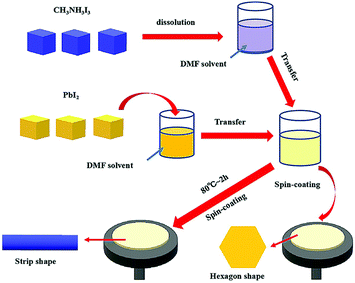 |
| | Fig. 1 Schematic illustration of the fabrication of the CH3NH3PbI3 perovskite. | |
The reaction was conducted in a nitrogen air atmosphere, not only to prevent the CH3NH3PbI3 perovskite from reacting with O2, but also to avoid the DMF solvent from evaporating from the solution with the increasing temperature. The PbI2 solution was added dropwise to ensure a smooth and steady structural transformation. After the reaction process, sample one was transferred to silica by a spin coating method for morphology characterization, as was sample two.
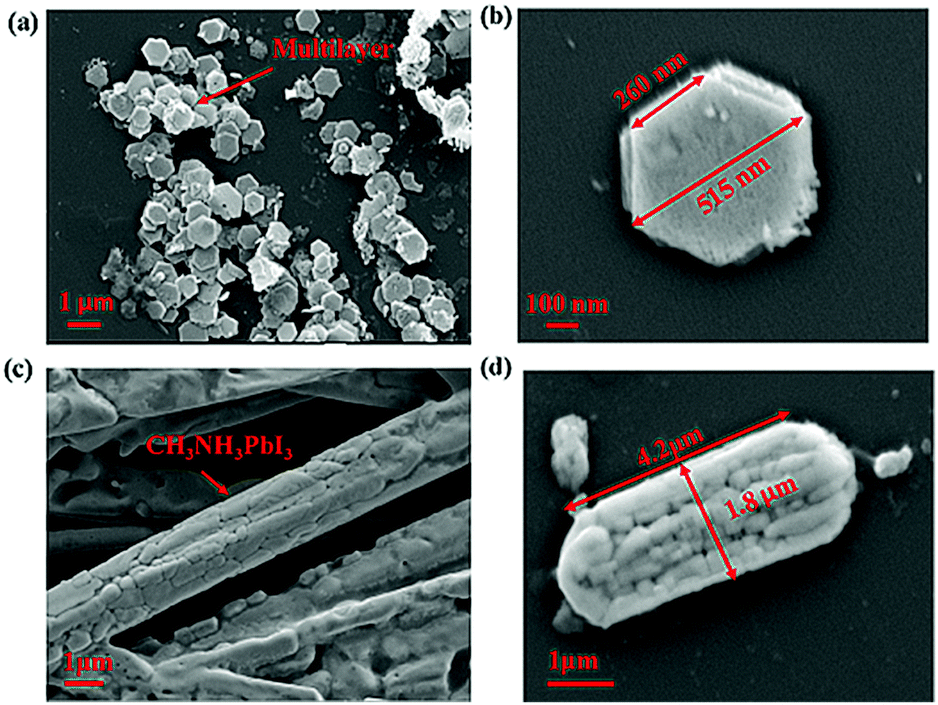
Fig. 2(a) shows a SEM image of sample one. As depicted, the prepared perovskite particle exhibited a regular hexagonal shape, and the side length of the subnanosheet perovskite was approximately 260 nm, as shown in Fig. 2(b). However, with the increase in the temperature to 80 °C, the structure was successfully transformed, as shown in the SEM image in Fig. 2(c). As depicted, the prepared perovskite particle exhibited a strip shape, with a length of approximately 4.2 μm and a width of approximately 1.8 μm, as shown in Fig. 2(d). We observed this phenomenon for two reasons: first, the DMF solvent applied during the preparation restricted the crystal growth, which ensured the overall shape of the CH3NH3PbI3 perovskite, but such restriction may differ in different directions; second, the thermodynamic factor played an important role in the crystal growth of the CH3NH3PbI3 perovskite, which accelerated the structural transformation due to the thermal energy. More details of the transformation mechanism will be discussed below.
 |
| | Fig. 2 (a and b) SEM image of the CH3NH3PbI3 perovskite prepared at room temperature; (c and d) SEM image of the CH3NH3PbI3 perovskite prepared at 80 °C. | |
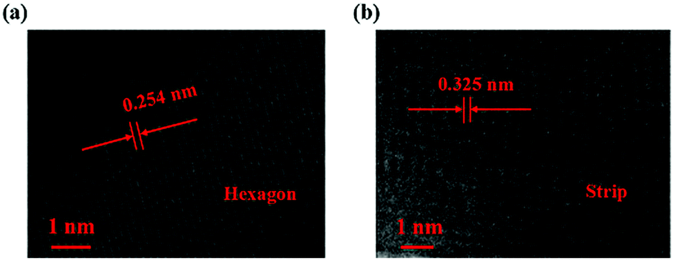
Fig. 3 shows the lattice fringes of the two different shaped perovskites, characterized by TEM to further study the inner structure. As depicted, the distance between the lattice fringes was 0.254 nm for the subnanosheet-shaped perovskite, while the distance was increased to 0.325 nm for the microwire shape. The results suggested that the inner structure of the CH3NH3PbI3 perovskite was modified due to the thermodynamic factor in the reaction.
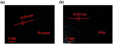 |
| | Fig. 3 (a and b) Lattice fringes of different CH3NH3PbI3 perovskite crystals characterized by TEM. | |
Fig. 4 shows a schematic illustration of the structural transformation of the perovskites influenced by the thermodynamic and solvent effects. As depicted, the purple balls, blue balls, and yellow balls represent the iodine atoms, CH3NH3 groups, and lead atoms, respectively. The CH3NH3PbI3 perovskite forms a tetragonal crystal with such atoms in a temperature range from 0 °C to 120 °C.23 In this structure, the iodine atoms located at the four sides of the tetragonal body are less stable than those on the upper and lower surfaces, resulting in easy rotation of the CH3NH3 group covalent bond with extra energy. In our work, the CH3NH3PbI3 perovskite was dispersed in DMF solvent, and the hexagonal shape tended to more easily form at room temperature because the direction restriction for the solvent was the same as that for the perovskite. However, the structure of the perovskite was modified with the increasing temperature and with the help of the DMF solvent due to the growth of the crystal, resulting in an increase in the lattice distance from 0.254 nm to 0.325 nm. This result indicated that such a change in the structure may alter the photoelectronic properties and stability of the perovskite, and further investigation of these two CH3NH3PbI3 perovskites should be performed in a future study.
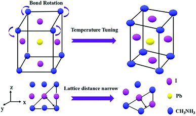 |
| | Fig. 4 Schematic illustration of the structural transformation of the CH3NH3PbI3 perovskite. | |
Fig. 5 shows the XRD analysis of these perovskites. The two samples were dried to a powder and subjected to incident X-rays at different diffraction angles ranging from 20° to 80°. All the characteristic diffraction peaks of the CH3NH3PbI3 perovskite are exhibited in the spectra, confirming the successful synthesis of CH3NH3PbI3. The diffraction intensity of the hexagonal perovskite crystal was significantly higher than that of the strip shape crystal, which indicated that good crystallizability was achieved for the hexagonal perovskite, and the lattice plane reflection was more intense due to the occurrence of covalent bond rotation and crystal growth. In addition, rather sharp peaks could be found in the spectra of the hexagonal perovskite, which were at diffraction angles of approximately 23°, 24.5°, 26°, 28°, 31.5°, 36.5°, 39°, 41°, and 43.5°, indicating a higher regularity and symmetry of the hexagonal shape than that of the strip shape; however, evidently broader peaks were found at diffraction angles of 52.5°, 55°, 61°, 62.5°, 67°, 68.5°, 74° and 77° for the hexagonal structure, and certain diffraction peaks, for example, those at angles of approximately 52.5° and 55°, showed little change compared to those of the strip-shaped CH3NH3PbI3 perovskite. These results suggested that the increase in the lattice distance may be due to the covalent bond rotation and growth of the perovskite crystal, resulting in a variation in the diffraction of the CH3NH3PbI3 perovskite crystal lattice, but more details need to be researched.
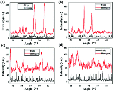 |
| | Fig. 5 XRD spectral analysis of different CH3NH3PbI3 perovskites. (a) Diffraction angle range from 20° to 35°; (b) diffraction angle range from 35° to 50°; (c) diffraction angle range from 50° to 65°; and (d) diffraction angle range from 65° to 80°. | |
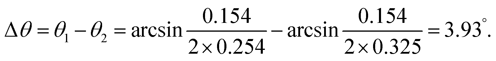
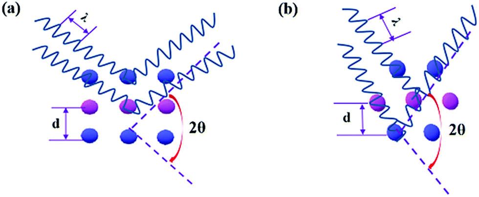
A schematic illustration of XRD characterization is shown in Fig. 6. As depicted, X-ray with a certain wavelength impinges on the atoms of the perovskite crystal, and the propagation direction is changed due to the surface reflection of the atoms. Additionally, incident diffraction also occurs when the X-rays pass through the space between two atoms. However, the reflection angle is altered with the position variation of the atoms, which results in a change in the lattice distance that correlates with the diffraction angle according to Bragg's law, expressed as follows:24
| | kλ = 2d![[thin space (1/6-em)]](https://www.rsc.org/images/entities/i_char_2009.gif) sin sin![[thin space (1/6-em)]](https://www.rsc.org/images/entities/char_2009.gif) θ, θ, | (2) |
where
kλ represents an integral multiple of the wavelength,
d is the lattice distance and
θ is half the diffraction angle. We assumed that the diffraction angles of sample one and sample two were
θ1 and
θ2, respectively. The deviation of the diffraction angle was Δ
θ, which was correlated with the covalent bond rotation angle of the CH
3NH
3PbI
3 perovskite. Here, the value of
k was regarded as 1, and the corresponding deviation value could be calculated as follows:
| |  | (3) |
 |
| | Fig. 6 Schematic illustration of XRD for the structural transformation of the CH3NH3PbI3 perovskite. | |
As shown, the diffraction angle decreased by 3.93° due to the increase in the lattice distance, as characterized by TEM.
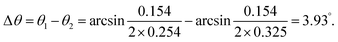
To further investigate the photoelectronic difference of these two CH3NH3PbI3 perovskites, more experiments were performed using spectroscopy. Fig. 7(a) and (b) shows the emission spectra and excitation spectra of these two samples. As depicted, the two emission spectra exhibited similar shapes, and two emission peaks were evidently found in sample one and sample two when excited by an incident wavelength of 360 nm. Compared to those for the strip-shaped CH3NH3PbI3 perovskite, the two emission peaks for the hexagonal-shaped perovskite, which were at approximately 480 nm and 515 nm, were both enhanced; in addition, a redshift of 5 nm was also found for the peak located at 515 nm. However, a much higher excitation intensity was achieved for the hexagonal CH3NH3PbI3 perovskite than for the stripe-shaped CH3NH3PbI3 perovskite, as shown in the excitation spectra, suggesting that a higher excitation efficiency was achieved with the hexagonal CH3NH3PbI3 perovskite. Fig. 7(c) and (d) shows a schematic illustration of the fluorescence emission mechanisms. The CH3NH3PbI3 molecule jumps from the ground state to the excitation state via energy absorption when excited by the incident beam. Due to the rotation of the covalent bond and crystal growth in the y-axis direction for the strip-shaped perovskite, the excitation cross-section became narrowed, contributing to the lower excitation efficiency. After being in the excitation state, the CH3NH3PbI3 molecule rapidly returns to the ground state with radiation and energy loss during emission, along with the occurrence of internal conversion or vibrational relaxation. Due to the higher symmetry and stability of the hexagonal structure, it possessed a 0.03 eV lower energy than the strip-shaped CH3NH3PbI3 perovskite, calculated according to the Planck equations as follows25
| |  | (4) |
 |
| | Fig. 7 (a) Emission spectra of different shaped CH3NH3PbI3 perovskites; (b) excitation spectra of different shaped CH3NH3PbI3 perovskites; and (c and d) schematic illustration of the fluorescence mechanisms for different shaped CH3NH3PbI3 perovskites. | |
The calculation result indicated that the redshift in the emission spectra around a wavelength of 515 nm further demonstrated the structural transformation of the CH3NH3PbI3 perovskite, resulting in a stability difference.
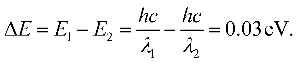
Fig. 8(a) shows the results of further investigation of these two samples using Raman spectroscopy excited by an incident laser with a wavelength of 632 nm. As depicted, the overall Raman scattering signal was weaker for the hexagonal-shaped CH3NH3PbI3 than for the strip-shaped CH3NH3PbI3. In addition, redshifts of the C–C and C–N vibrations at approximately 1500 cm−1 and 1750 cm−1, respectively, were observed in the hexagonal-shaped CH3NH3PbI3 compared to the strip-shaped CH3NH3PbI3. The electrons around the perovskite molecules interact with photons when excited, leading to 3D atomic vibration, and polarization occurs, as shown in Fig. 8(b). In addition to the 3D vibration, the electrons also travel around the hexagonal plane that consists of atoms but not around the microwires, which could stabilize the CH3NH3PbI3 molecule and weaken the polarization. The results suggested that lower scattering was achieved for the hexagonal-shaped CH3NH3PbI3 perovskite and further confirmed the higher stability of the hexagonal-shaped CH3NH3PbI3 perovskite due to its symmetry.
 |
| | Fig. 8 (a) Raman spectra of different shaped CH3NH3PbI3 perovskites and (b) schematic illustration of the Raman scattering for different shaped CH3NH3PbI3 perovskites. | |
Photon capture is a critical factor for a CH3NH3PbI3 perovskite when applied to optoelectronic research, such as solar cell applications or photodetector applications.26–31Fig. 9(a) shows the UV-vis spectra of the two samples. As depicted, broad absorption across the UV-vis region was found for both samples; however, the hexagonal-shaped CH3NH3PbI3 exhibited higher absorption than the strip-shaped CH3NH3PbI3. In addition, the absorption peak originated from the transition of unbound electrons, which was located at approximately 380 nm for the strip-shaped CH3NH3PbI3, while a redshift of ∼20 nm was observed for the hexagonal-shaped CH3NH3PbI3. The energy deviation after structural transformation can be calculated according to the following equation:
| |  | (5) |
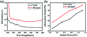 |
| | Fig. 9 (a) UV-vis spectra of two different shaped CH3NH3PbI3 perovskites and (b) absorption measurement of two different shaped CH3NH3PbI3 perovskites, subjected to an incident laser with a wavelength of 468 nm. | |
The calculation results suggested that the redshift of the absorption peak for the hexagonal CH3NH3PbI3 was attributed to the electron conjugation effect and the higher symmetry of the structure, which may explain the higher fluorescence excitation efficiency. Fig. 9(b) shows the absorption measurement results of these two samples when subjected to an incident laser with a wavelength of 468 nm for further demonstration of the absorption mechanism. Here, we defined the absorption ratio αR as follows:
| |  | (6) |
where
P1 is the absorbed power and
P2 is the initial power of the incident laser. As depicted, the absorption ratio increased for both perovskites with the increasing initial power from 0.25 W to 1.15 W. However, the absorption ratios of the hexagonal-shaped CH
3NH
3PbI
3 were all higher than those of the strip-shaped CH
3NH
3PbI
3, and the highest absorption increase of 50% was achieved for the hexagonal-shaped CH
3NH
3PbI
3 for an initial incident power of 0.25 W. These results well coincided with the UV-vis spectrum characterization and further supported the above studies.
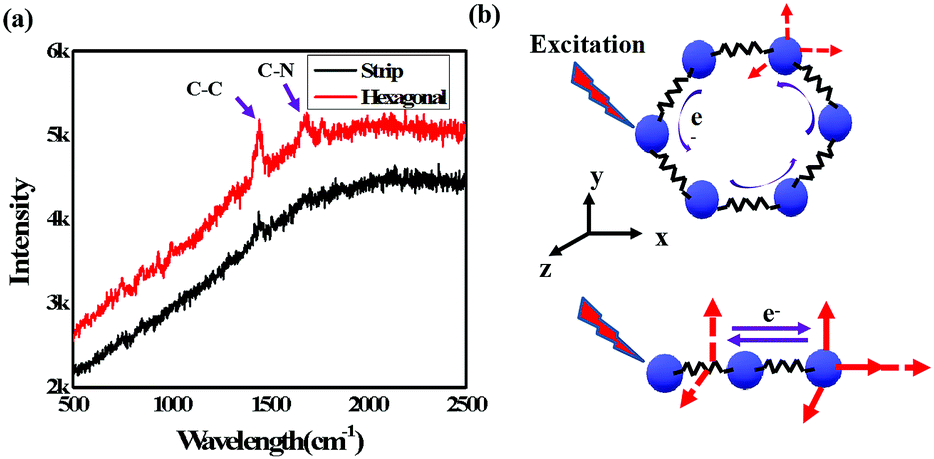
In addition to photon capture, the conductivity is another important factor for solar cell application.33–36Fig. 10 shows the experimental scheme of the conductivity investigation, which was performed on the CH3NH3PbI3 perovskite combined with ITO glass under different voltage excitation. As shown in Fig. 11(a), the resistance of the hexagonal-shaped CH3NH3PbI3 decreased from 14 Ω to 13.5 Ω under an applied voltage of 1 V when it transformed into a microwire shape, and the largest decrease of 2.5 Ω, from 18 Ω to 15.5 Ω, was achieved when the applied voltage was 5 V. To the best of our knowledge, the resistance of the CH3NH3PbI3 perovskite would increase with the increasing voltage excitation, and we attributed the reason to the higher heat energy accumulated due to the electric field, resulting in more collision of excitons and an increase in resistance. This result suggested that the structural transformation optically changed the resistivity of the CH3NH3PbI3 perovskite, resulting in better conductivity of the strip-shaped CH3NH3PbI3 compared to the hexagonal-shaped CH3NH3PbI3, which may be due to the strip-shaped structure being more suitable for electron migration.
 |
| | Fig. 10 Experimental scheme of resistance measurement for different CH3NH3PbI3 perovskites. | |
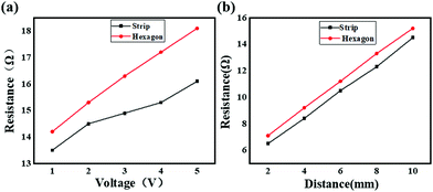 |
| | Fig. 11 (a) Resistance–voltage curves of the two different shaped CH3NH3PbI3 perovskites on ITO glass substrates and (b) resistances of the two different shaped CH3NH3PbI3 perovskites on ITO glass, with the length of the ITO glass ranging from 2 mm to 10 mm. | |
Based on the above study, the resistivity, which was deeply impacted by the structure of the material, was a critical reflection of the conductivity. Regardless of this, different resistivity perovskite materials may be suitable for different applications, for example, lower resistivity and higher photon absorption perovskite materials are more suitable for solar cell applications, but higher resistivity materials would be more suitable for optical applications.37–39 To thoroughly analyze the conductivity of these two different shaped CH3NH3PbI3 perovskites coated on ITO glass, the resistance of the ITO glass coated with different perovskites was tested for different lengths. The experimental scheme is shown in Fig. 10, and the results are shown in Fig. 11(b). As depicted, the resistances of both the hexagonal-shaped and strip-shaped CH3NH3PbI3 crystals linearly increased with the increasing length of the ITO glass, which indicated that a well-distributed CH3NH3PbI3 perovskite was coated on the ITO glass. In addition, the resistances of the hexagonal-shaped CH3NH3PbI3 perovskite were all higher than those of the strip-shaped structure for lengths ranging from 2 mm to 10 mm, as shown in Fig. 11(a). This further confirmed that the resistivity of the CH3NH3PbI3 perovskite can be effectively altered through structural transformation.
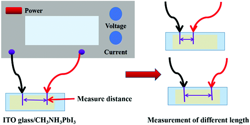
The stability of a perovskite material directly affects the operation life of a device when applied as an absorber in solar cells.40 In general, the stability of a perovskite, which includes the conductivity and photon capture, decreases with the increasing storage time due to the redox reaction.41 To analyze the stability of these two samples, absorption experiments and resistance examinations were both performed. In the absorption experiment, the CH3NH3PbI3 perovskite samples exposed to air for several days were subjected to an incident laser with a wavelength of 468 nm and compared with the samples not exposed to air, and the result is shown in Fig. 12(a). Here, we defined the absorption deviation σP expressed as follows:
| |  | (7) |
where
P1 is the absorbed power of the CH
3NH
3PbI
3 perovskite not exposed to air, and
P2 is the absorbed power of that exposed to air for several days. As depicted, the absorbed power decreased as the exposure time increased from 3 days to 21 days. However, the absorbed power deviation of the hexagonal-shaped CH
3NH
3PbI
3 could be controlled at 2.5%, while that of the strip-shaped CH
3NH
3PbI
3 was approximately 5%.
Fig. 12(b) shows the resistance deviation of these two types of CH
3NH
3PbI
3 perovskite, which was defined as follows:
| |  | (8) |
where
R1 is the resistance of the CH
3NH
3PbI
3 perovskite not exposed to air and
R2 is the resistance of that exposed to air for several days. As depicted, the resistance increased as the exposure time increased from 3 days to 21 days. However, the resistance deviation of the hexagonal-shaped CH
3NH
3PbI
3 could be controlled at 3.3%, which was lower than that of the strip-shaped CH
3NH
3PbI
3 with a resistance deviation of approximately 4.8%. These results suggested that the stability of the hexagonal-shaped CH
3NH
3PbI
3 was better than that of the strip-shaped CH
3NH
3PbI
3.
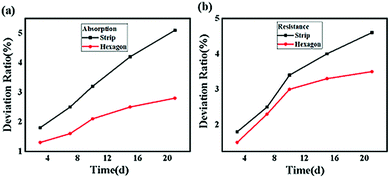 |
| | Fig. 12 (a) Absorption deviation ratio of different shaped CH3NH3PbI3 perovskites on different days and (b) resistance deviation ratio of different shaped CH3NH3PbI3 perovskites on different days. | |
3 Conclusions
In conclusion, we successfully synthesized microwire- and subnanosheet-shaped CH3NH3PbI3 perovskites via temperature tuning and solvent effects, which were characterized by SEM and TEM, suggesting that the lattice distance increased from 0.254 nm to 0.354 nm when the hexagonal structure was transformed into a microwire structure. Further analysis showed that the structural transformation originated from the covalent bond rotation and crystal growth in the y-axis direction, and the calculation results showed that the rotation angle decreased by 3.93° after the structural transformation, which was attributed to the subnanosheet having a 0.03 eV lower energy than that of the microwire shape. Compared to the microwire-shaped CH3NH3PbI3, the power absorption of the subnanosheet increased by 25% to 50% when the incident power ranged from 1.15 W to 0.25 W. This result suggested that the optical characteristics of the hexagonal-structured CH3NH3PbI3 perovskite were better than those of the microwire-shaped CH3NH3PbI3 perovskite. The electrical measurement results further indicated that better conductivity was achieved for the microwire-shaped CH3NH3PbI3 perovskite than for the subnanosheet-shaped CH3NH3PbI3 perovskite. However, the stability test showed that the absorbed power deviation of the subnanosheet CH3NH3PbI3 could be controlled at 2.5% when exposed to air for 21 days, while that of the strip-shaped CH3NH3PbI3 was approximately 5%. In addition, the resistance deviation of the hexagonal-shaped CH3NH3PbI3 could be controlled at 3.3%, which was lower than that of the strip-shaped CH3NH3PbI3 with a resistance deviation of approximately 4.8%. These results have experimentally and theoretically demonstrated the structural transformation mechanism of a CH3NH3PbI3 perovskite and suggest that the hexagonal structure CH3NH3PbI3 perovskite is more suitable for optical applications, whereas the microwire structure may be more suitable for electrical applications.
Conflicts of interest
There are no conflicts to declare.
Acknowledgements
This work was partly financed by the Science and Technology Innovation Commission of Shenzhen (JCYJ20170412111625378).
Notes and references
- J. Y. Jeng, Y. F. Chiang, M. H. Lee, S. R. Peng, T. F. Guo, P. Chen and T. C. Wen, Adv. Mater., 2013, 25, 3727 CrossRef CAS
 .
.
- H. S. Kim, J. W. Lee, N. Yantara, P. P. Boix, S. A. Kulkarni, S. Mhaisalkar, M. Gratzel and N. G. Park, Nano Lett., 2013, 13, 2412 CrossRef CAS .
- E. Strelcov, Q. F. Dong, T. Li, J. S. Chae, Y. C. Shao, Y. H. Deng, A. Gruverman, J. S. Huang and A. Centrone, Sci. Adv., 2017, 3, 1602165 CrossRef .
- T. Oku, Y. Y. Ohishi and N. Ueoka, RSC Adv., 2018, 19, 12389 Search PubMed .
- D. Webber, C. Clegg, A. W. Mason, S. A. March, I. G. Hill and K. C. Hall, Appl. Phys. Lett., 2017, 111, 121905 CrossRef .
- M. Becker and M. Wark, J. Phys. Chem. C, 2018, 122, 3548 CrossRef CAS .
- L. H. Zhang and P. H. L. Sit, J. Mater. Chem. A, 2017, 5, 9042 RSC .
- Y. Yu, Y. T. Zhang, Z. Zhang, H. T. Zhang, X. X. Song, M. X. Cao, Y. L. Che, H. T. Dai, J. B. Yang, J. L. Wang, H. Zhang and J. Q. Yao, J. Phys. Chem. Lett., 2017, 8, 445 CrossRef CAS .
- J. Ma and L. W. Wang, Nano Lett., 2017, 17, 3646 CrossRef CAS .
- W. D. Zhu, L. Kang, T. Yu, B. H. Lv, Y. R. Q. Wang, X. Y. Chen, X. Y. Wang, Y. Zhou and Z. G. Zou, ACS Appl. Mater. Interfaces, 2017, 9, 6104 CrossRef CAS .
- A. Kovalsky, L. L. Wang, G. T. Marek, C. Burda and J. S. Dyck, J. Phys. Chem. C, 2017, 121, 3228 CrossRef CAS .
- R. A. Kerner and B. P. Rand, J. Phys. Chem. Lett., 2017, 8, 2298 CrossRef CAS .
- G. W. Ji, G. H. J. Zheng, B. Zhao, F. Song, X. N. Zhang, K. C. Shen, Y. G. Yang, Y. M. Xiong, X. Y. Gao, L. Cao and D. C. Ci, Phys. Chem. Chem. Phys., 2017, 19, 6546 RSC .
- Y. Liu, F. S. Li, C. P. Veeramalai, W. Chen, T. L. Guo, C. X. Wu and T. W. Kim, ACS Appl. Mater. Interfaces, 2018, 9, 11662 CrossRef .
- W. G. Zhao, Z. Yao, F. Y. Yu, D. Yang and S. Z. Liu, Adv. Sci., 2018, 5, 1700131 CrossRef .
- L. C. Chen, K. L. Lee, W. T. Wu, C. F. Hsu, Z. L. Tseng, X. H. Sun and Y. T. Kao, Nanoscale Res. Lett., 2018, 6, 13140 Search PubMed .
- Z. B. Yao, W. L. Wang, H. P. Shen, Y. Zhang, Q. Luo, X. W. Yin, X. Z. Dai, J. B. Li and H. Li, Sci. Technol. Adv. Mater., 2017, 18, 254 CrossRef .
- J. H. Heo, M. Jahandar, S. J. Moon, C. E. Song and S. H. Im, J. Mater. Chem. C, 2017, 5, 2883 RSC .
- M. Afzaal, B. Salhi, A. A. Ahmed, H. M. Yates and A. S. Hakeem, J. Mater. Chem. C, 2017, 5, 8366 RSC .
- L. C. Chen, Y. S. Lin, P. W. Tang, C. Y. Tai, Z. L. Tseng, J. H. Lin, S. H. Chen and H. C. Kuo, Nanoscale, 2017, 9, 17802 RSC .
- W. C. Lai, K. W. Lin, T. F. Guo, P. Chen and Y. Y. Liao, Appl. Phys. Lett., 2018, 112, 071103 CrossRef .
- Z. Hong, J. Zhao, S. J. Li, B. C. Cheng, Y. H. Xiao and S. J. Lei, Nanoscale, 2019, 11, 3360 RSC .
- J. Y. Jeng, Y. F. Chiang, M. H. Lee, S. R. Peng, T. F. Guo, P. Chen and T. C. Wen, Adv. Mater., 2013, 35, 3727 CrossRef .
- J. H. Im, I. H. Jang, N. Pellet, M. Gratzel and N. G. Park, Nat. Nanotechnol., 2014, 9, 927 CrossRef CAS .
- Y. X. Zhao and K. Zhu, J. Phys. Chem. C, 2014, 118, 9412 CrossRef CAS .
- Y. Y. Dang, Y. Liu, Y. X. Sun, D. S. Yuan, X. K. Liu, W. Q. Lu, G. F. Liu, H. B. Xia and X. T. Tao, CrystEngComm, 2015, 17, 665 RSC .
- W. Y. Tan, P. P. Cheng, Y. W. Zhang, J. M. Liang, X. D. Chen, Y. D. Liu and Y. Min, J. Mater. Chem. C, 2019, 7, 6004 RSC .
- G. Kakavelakis, E. Gagaoudakis, K. Petridis, V. Petromichelaki, V. Binas, G. Kiriakidis and E. Kymakis, ACS Sens., 2018, 3, 135 CrossRef CAS .
- P. F. Li, Y. Chen, T. S. Yang, Z. Y. Wang, H. Lin, Y. H. Xu, L. Li, H. R. Mu, B. N. Shivananju, Y. P. Zhang, Q. L. Zhang, A. L. Pan, S. J. Li, D. Y. Tang, B. H. Jia, H. Zhang and Q. L. Bao, ACS Appl. Mater. Interfaces, 2017, 9, 12759 CrossRef CAS .
- N. Dong, X. W. Fu, G. Lian, S. Lv, Q. L. Wang, D. L. Cui and C. P. Wong, ACS Appl. Mater. Interfaces, 2018, 10, 8393 CrossRef CAS .
- R. K. Singh, R. Kumar, N. H. Jain, M. T. Kuo, C. P. Upadhyaya and J. Singh, Appl. Nanosci., 2019, 6, 6078 Search PubMed .
- M. U. Rothmann, W. Li, Y. Zhu, U. Bach, L. Spiccia, I. Etheridge and Y. B. Cheng, Nat. Commun., 2017 DOI:10.1038/ncomms14547 .
- E. Horvath, M. Spina, Z. Szekrenyes, K. Kamaras, R. Gaal, D. Gachet and L. Forro, Nano Lett., 2014, 14, 6761 CrossRef CAS .
- D. Y. Liu, S. S. Li, F. Bian and X. Y. Meng, Materials, 2018, 11, 1141 CrossRef .
- W. R. Zhou, P. C. Zhou, X. Y. Lei, Z. M. Fang, Q. Liu, T. Chen, H. L. Zeng, L. M. Ding, J. Zhu, S. Y. Dai and S. F. Yang, ACS Appl. Mater. Interfaces, 2018, 10, 1897 CrossRef CAS .
- F. Qin, W. Meng, J. C. Fan, C. Ge, B. W. Luo, R. Ge, L. Hu, F. Y. Jiang, T. F. Liu, Y. Y. Jiang and Y. H. Zhou, ACS Appl. Mater. Interfaces, 2017, 9, 26045 CrossRef CAS .
- M. Becker and M. Wark, J. Phys. Chem. C, 2018, 122, 3548 CrossRef CAS .
- L. H. Li, J. L. Mi, Y. C. Yong, B. D. Mao and W. D. Shi, J. Mater. Chem. C, 2018, 6, 8226 RSC .
- Z. Y. Wang, Q. D. Ou, Y. P. Zhang, Q. H. Zhang, H. Y. Hoh and Q. L. Bao, ACS Appl. Mater. Interfaces, 2018, 10, 24258 CrossRef CAS .
- M. Kumar, H. S. Kim, D. Y. Park, M. S. Jeong and J. D. Kim, RSC Adv., 2018, 8, 25206 Search PubMed .
- L. Ciric, K. Ashby, M. Spina, M. Duchamp, B. Nafradi, M. Kollar, L. Forro and E. Horvath, Appl. Phys. Lett., 2018, 112, 111901 CrossRef .
|
| This journal is © The Royal Society of Chemistry 2020 |

 Open Access Article
 This Open Access Article is licensed under a Creative Commons Attribution-Non Commercial 3.0 Unported Licence
 * and
Qiao
Wen
* and
Qiao
Wen