
 Open Access Article
 This Open Access Article is licensed under a
 Creative Commons Attribution 3.0 Unported Licence
Atomic-scale structure and chemical sensing application of ultrasmall size-selected Pt nanoparticles supported on SnO2
Stephan
Steinhauer†
 *a,
Eva
Lackner
b,
Florentyna
Sosada-Ludwikowska
b,
Vidyadhar
Singh‡
a,
Johanna
Krainer
b,
Robert
Wimmer-Teubenbacher
b,
Panagiotis
Grammatikopoulos
a,
Anton
Köck
*b and
Mukhles
Sowwan
a
*a,
Eva
Lackner
b,
Florentyna
Sosada-Ludwikowska
b,
Vidyadhar
Singh‡
a,
Johanna
Krainer
b,
Robert
Wimmer-Teubenbacher
b,
Panagiotis
Grammatikopoulos
a,
Anton
Köck
*b and
Mukhles
Sowwan
a
aNanoparticles by Design Unit, Okinawa Institute of Science and Technology (OIST) Graduate University, 1919-1 Tancha, Onna-Son, Okinawa, 904-0495, Japan
bMaterials Center Leoben Forschungs GmbH, Roseggerstrasse 12, 8700 Leoben, Austria. E-mail: anton.koeck@mcl.at
First published on 14th October 2020
Abstract
The surface reactivity of metal oxide materials can be enhanced by nanoparticle decoration, which is of crucial importance in catalysis and chemical sensing applications. Here, we employ ultrasmall Pt nanoparticles for the functionalization of tin oxide (SnO2) thin film-based chemoresistive sensors integrated in complementary metal-oxide-semiconductor technology. Size-selected Pt nanoparticles with an average diameter below 2 nm were fabricated by a solvent-free gas-phase synthesis approach and deposited onto the SnO2 sensing layer surfaces, which resulted in carbon monoxide sensing properties with minimized humidity interference. The atomic-scale structure of ultrasmall Pt nanoparticles supported on SnO2 was studied by in situ transmission electron microscopy, performing heating experiments in reactive gas atmosphere relevant for sensor operation. Our results reveal the formation of Pt oxide phases and nanoparticle–support interactions, which contributes to a more detailed understanding of the structure–property relationships in the SnO2–Pt nanomaterial system.
1 Introduction
Metal oxide nanomaterials have been extensively studied for the realization of high-performance, low-cost devices for chemical sensing of gas molecules, which is relevant in multiple application areas including environmental air quality monitoring as well as detection of toxic and explosive gases. Significant progress has been achieved in optimizing the sensor device properties by tailoring the nanostructure morphology and by multi-component nanomaterial approaches including surface modification and additive doping.1,2 Tin oxide (SnO2), a wide band gap n-type semiconductor, is one of the most commonly used sensing materials. It is well established that the performance of SnO2-based devices can be enhanced by employing sensing elements based on heterostructures3–7 or by decorating the metal oxide with catalytic noble metal additives8,9 including Pt nanoparticles.10–14 In a similar way, different SnO2–Pt nanomaterial configurations were employed to promote chemical reactions in (electro-) catalysis.15–18 Previous reports correlating the chemoresistive response of Pt-doped SnO2 thick film devices with spectroscopy results19,20 provided crucial insights into the underlying mechanisms of gas–solid interactions. However, it is of vital importance to study the atomic-scale morphology of SnO2–Pt nanomaterials subjected to reactive gas atmospheres at elevated temperatures to obtain more detailed knowledge on the structure–property relationships in this material system.In this article, we present gas-phase synthesis of ultrasmall Pt nanoparticles (average diameter <2 nm) for the surface decoration of nanocrystalline SnO2 thin films and SnO2 nanowires. Magnetron sputtering inert-gas condensation, a versatile technique for the growth of single- and multicomponent nanoparticles with controlled size and morphology,21–23 was employed for the deposition of pre-formed, size-selected Pt nanoparticles. A wide range of nanoparticle functionalities has been achieved with this method, e.g., percolating nanoparticle films for chemoresistive sensing,24–30 nanoparticle-decorated metal oxide nanowire devices for chemoresistive sensing,31–33 supported nanoparticles for catalysis and electrochemistry,34–37 magnetic nanoparticles,30,38–40 nanoparticles embedded in multi-layered anodes for lithium ion batteries41 and nanoportals for hydrogen storage applications.42 Here, we demonstrate a new approach for the surface functionalization of micro-machined chemical sensor devices realized in complementary metal-oxide-semiconductor (CMOS) technology, in particular by depositing ultrasmall Pt nanocatalysts by magnetron sputtering inert-gas condensation onto nanocrystalline SnO2 thin films integrated on a suspended microhotplate platform. We focus on studying the sensing performance for the toxic gas carbon monoxide (CO) in humid atmosphere, which is highly relevant for safety applications as well as environmental monitoring. Importantly, it was found that our CMOS-integrated SnO2–Pt nanomaterial system is ideally suited for CO sensing with minimized humidity interference. Furthermore, in situ transmission electron microscopy (TEM) experiments are presented, studying the thermal stability of ultrasmall Pt nanoparticles in a reactive gas atmosphere. Using single-crystalline SnO2 nanowire supports as model system, we investigate the atomic-scale structure of the nanocatalysts after heating in an oxygen environment. Our results show that nanoparticle–support interactions influence the nanoparticle morphology, leading to oxidized Pt clusters with elongated shapes and with crystal structures epitaxially aligned to the SnO2 support.
2 Methods
2.1 Synthesis of SnO2 thin films and nanowires
SnO2 thin films with a thickness of 50 nm were deposited by spray pyrolysis using tin chloride pentahydrate in ethyl acetate as precursor material. The samples were placed on a hotplate at a temperature of 400 °C and the solution was sprayed by an atomizing nozzle using N2 as carrier gas.43 Subsequent annealing was performed at 400 °C in ambient air to obtain nanocrystalline SnO2 structure. Deposition was performed on TEM support films (silicon nitride, thickness 15 nm) for characterization and on CMOS chips with integrated microhotplate structures for chemoresistive sensing experiments (see Section 2.4). SnO2 nanowires were synthesized in a constant Ar gas flow (1000 sccm) at 900 °C for 1 h using SiO2/Si substrates with a Cu catalyst as growth substrate and SnO2 thin films (thickness 500 nm; spray pyrolysis deposition as described above) on a separate SiO2/Si sample as source material.432.2 Deposition of size-selected Pt nanoparticles
Pt nanoparticles were fabricated by magnetron sputtering inert-gas condensation in a high-vacuum deposition system using a cluster beam source combined with an in-line quadrupole mass filter (QMF) for size selection.22 The base pressure of the instrument was ∼10−8 mbar. During nanoparticle synthesis, the main chamber pressure was ∼10−4 mbar and the aggregation zone pressure was ∼10−1 mbar. Size-selected Pt nanoparticles were directly deposited on carbon TEM support films, Si substrates (root mean square roughness 0.2 nm) for atomic force microscopy (AFM) characterization (Bruker Multimode 8 in tapping mode), silicon nitride TEM support films covered with SnO2 thin films, membrane-based TEM heating chips with mechanically-transferred SnO2 nanowires and CMOS-integrated SnO2 thin film devices. The synthesis conditions were a magnetron power of 3 W, a constant flow of 70 sccm Ar and 5 sccm He, and an aggregation length of 80 mm. The substrate holder was rotated at 2 rpm to ensure homogeneous nanoparticle deposition.2.3 Transmission electron microscopy characterization and in situ heating experiments in oxygen atmosphere
An FEI Titan Environmental TEM equipped with a spherical aberration corrector for the objective lens was used at an operation voltage of 300 kV for imaging, diffraction and energy-dispersive X-ray spectroscopy. The Pt nanoparticle size distribution was obtained from low-magnification TEM micrographs by means of automated image analysis with the software ImageJ, measuring projected areas and assuming spherical geometries. In situ heating experiments of SnO2 thin films/SnO2 nanowires decorated with Pt nanoparticles were performed at an oxygen pressure of 20 mbar and a temperature of 350 °C for 30 min. The thin films on silicon nitride TEM support films were heated with a furnace-type Gatan heating holder, whereas the nanowires were heated on membrane-based heating chips using a Protochips Aduro holder.2.4 Device fabrication and chemoresistive sensing
The CMOS integration of SnO2 thin film sensors was achieved by employing spray pyrolysis as back-end fabrication step. Photolithography followed by Ar ion etching was performed for patterning the SnO2 thin film. The CMOS chips were realized in standard 0.35 μm technology (ams AG) and the microhotplate devices were under-etched by an isotropic XeF2 dry etching process to ensure thermal insulation from the rest of the substrate.44,45 The performance of CMOS-integrated sensors was evaluated in an automated measurement setup. Synthetic air at three relative humidity levels (humidification via water bubbler; relative humidity continuously measured with a commercial sensor) was employed as background gas. Pulses of CO at concentrations between 10 ppm and 200 ppm were introduced by adjusting the flow of background and target gas by mass flow controllers at corresponding ratios (constant total gas flow of 1000 sccm). The microhotplates were heated to the operation temperatures 350 °C, 375 °C and 400 °C by biasing an embedded polysilicon resistor and the SnO2 sensing layer resistance was measured via electrical contacts connected to underlying metallization layers and contact pads. The relative resistance changes due to the interaction with CO, i.e., the sensor response S, was evaluated according to S = (Rair − Rgas)/Rair, where Rgas is the resistance in test gas and Rair is the resistance in background gas.3 Results and discussion
Pt nanoparticles were synthesized by magnetron sputtering inert-gas condensation and their size distribution was adjusted by fine-tuning the deposition parameters, in particular the magnetron power, the gas flow and the QMF settings, resulting in size control in the range of 1 nm to 5 nm. Here, we focus on ultrasmall Pt nanoparticles with average diameters below 2 nm (synthesis conditions detailed in Methods section), which can be seen in the low-magnification TEM micrograph in Fig. 1a. The nanoparticles were well-dispersed with no signatures of agglomeration and their density was determined to be around 4600 μm−2 for 20 min deposition time. Size distributions obtained by TEM and AFM characterization were in good agreement and average nanoparticle sizes of 1.60 nm (TEM) and 1.85 nm (AFM) were found.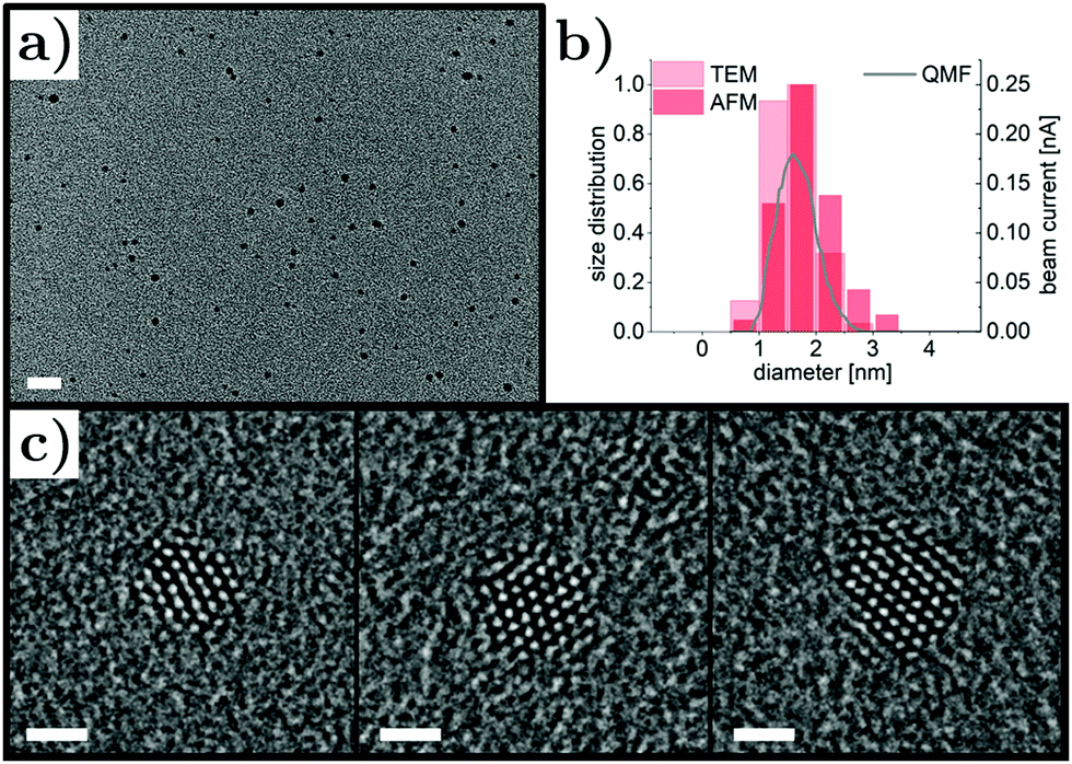 | ||
| Fig. 1 (a) Low-magnification transmission electron micrograph showing well-dispersed size-selected Pt nanoparticles on a carbon support film (scale bar 10 nm). (b) Nanoparticle size distributions obtained from transmission electron microscopy (TEM) and atomic force microscopy (AFM) characterization compared to the quadrupole mass filter (QMF) beam current recorded during nanoparticle deposition. (c) High-resolution transmission electron micrographs of three representative Pt nanoparticles with single-crystalline structure (scale bars 1 nm). | ||
In Fig. 1b, the distributions are shown with the beam current signal of the QMF in the deposition system, demonstrating excellent nanoparticle size control. The crystal structure of the Pt nanoparticles was studied by aberration-corrected high-resolution TEM; three representative micrographs are presented in Fig. 1c. The nanoparticles were imaged along the (110) zone axes and the lattice spacings were consistent with the face-centered cubic structure of Pt. Although no extended facets were present due to the ultrasmall size, a tendency for faceting with (111) surfaces was observed, which could be explained in terms of Pt surface energies46 and thermodynamic equilibrium shape considerations.47 In magnetron sputtering inert-gas condensation, atoms are sputtered off the target material by a plasma process, cool down via collisions with Ar gas atoms and form clusters after reaching temperatures suitable for bond formation. A recent study showed that the initial cluster formation of noble metals during gas-phase synthesis can be significantly influenced by their electronic configuration.48 It is expected that the observed morphology of the Pt nanoparticles presented here is a result of comparatively slow cluster nucleation due to the high stability of dimers compared to trimers and, hence, slowed down growth kinetics, which reduces the nanoparticle yield but favors homogeneity. The latter is of significant importance due to the size and shape dependence of Pt nanoparticle catalytic activity.49–51
The ultrasmall size-selected Pt nanoparticles were applied for the surface functionalization of CMOS-integrated chemical sensors based on nanocrystalline SnO2 thin films. The scanning electron microscopy image in Fig. 2a shows a typical sensor device, consisting of a microhotplate (∼70 × 70 μm) suspended on four arms with electrical contacts connected to the underlying metallization layers and the gas-sensitive SnO2 layer on top. During the magnetron sputtering-based gas-phase synthesis process, the pre-formed Pt nanoparticles were transported directly onto the CMOS chips by means of a pressure differential between the aggregation zone and the deposition chamber, which enables nanoparticle decoration without requiring additional precursors or solvents. After passing through the QMF for size filtration, the nanoparticles are deposited onto the sample in the soft-landing regime,21 which minimizes damage to both the nanoparticles and the substrate resulting from the impact during deposition. The performance of pristine and nanoparticle-decorated devices was characterized for CO sensing in humid atmosphere at operation temperatures between 350 °C and 400 °C, corresponding to microhotplate power consumptions between 12.3 mW and 13.9 mW. Measurement results at 400 °C and 53% relative humidity are presented in Fig. 2b showing an electrical resistance decrease of the SnO2-based sensor device during exposure to the reducing gas CO, which is expected for n-type metal oxide semiconductors.52 The sensor response S was evaluated for pristine and nanoparticle-decorated sensors for three relative humidity levels (Fig. 2c). The sensor response S of the nanoparticle-decorated device was comparable to the pristine SnO2 device at low CO concentrations but showed generally lower responses at higher CO concentrations. The pristine sensor exhibited significant humidity interference effects with decreasing CO response for increased relative humidity levels, which is commonly observed for undoped SnO2 materials.53 In contrast, Pt nanoparticle decoration led to sensor responses with negligible humidity interference, demonstrating the marked impact of surface functionalization on the device performance. The influence of metal oxide doping/surface decoration on humidity interference effects in CO sensing have been comprehensively studied in previous literature. Reduced humidity interference was reported for Pd additives,54–57 NiO loading,58 Sb doping,59 and Pt doping;19,20,54,55 size-dependent effects were reported for Pd nanoparticle surface decoration.60 However, in most cases thick film-based devices and related synthesis/doping approaches have been used, which complicates a direct comparison with the presented results due to differences in sensor morphology and in the way dopants are incorporated into the sensing layer. Hence, the CO sensing characteristics of our SnO2–Pt nanomaterial system and its atomic-scale structure will be further discussed to gain a better understanding of the underlying solid–gas interaction and sensor transduction mechanisms.
 | ||
| Fig. 2 (a) Schematic of magnetron sputtering inert-gas condensation source for the nanoparticle decoration of chemical sensor devices realized in complementary metal-oxide-semiconductor (CMOS) technology. The scanning electron microscopy image shows a microhotplate device suspended on four arms with SnO2 sensing layer (scale bar 10 μm). (b) Electrical resistance change of SnO2 thin film decorated with Pt nanoparticles during exposure to six pulses with increasing CO concentrations between 10 ppm and 200 ppm (53% relative humidity, 400 °C operation temperature). (c) Comparison of sensor response S of pristine and nanoparticle-decorated SnO2 sensor device for three different relative humidity levels (400 °C operation temperature). | ||
Sensor characterization at lower operation temperatures of 350 °C and 375 °C (performed before the 400 °C measurement) showed mostly similar characteristics. However, the sensor device decorated with Pt nanoparticles was very reactive to CO in the beginning of the 350 °C measurement cycle, showing atypical gas response behavior that diminished over time. After stabilization, the sensor response at 350 °C was comparable to the case of 400 °C presented above. It is assumed that the Pt nanoparticles undergo changes in structure and/or chemical composition, which motivated us to further study the ultrasmall Pt nanocatalysts supported on SnO2 by means of in situ TEM.
As a first step, samples based on nanocrystalline SnO2 layers deposited on silicon nitride TEM support films were investigated. A high-resolution TEM micrograph and a selected area electron diffraction pattern is presented in Fig. 3a. The polycrystalline structure is evident with grain sizes well below the film thickness of 50 nm, resulting in a relatively compact film. The rutile SnO2 phase with tetragonal structure was found and typical grain sizes around 4 nm were observed. These results are consistent with previous characterization data of the morphology, chemical composition and crystalline structure of nanocrystalline SnO2 thin films obtained by the same method.61,62 To identify ultrasmall Pt nanoparticles, bright field imaging was not suitable due to the considerably larger SnO2 film thickness and thus high-angle annular dark field imaging was employed. Nanoparticles could be seen as spots with brighter contrast (Fig. 3b) due to the large atomic number of Pt, which was confirmed by energy-dispersive X-ray spectroscopy (note that the Cu Kα signal can be attributed to the sample holder). The SnO2 thin film decorated with Pt nanoparticles was in situ heated to 350 °C at an oxygen pressure of 20 mbar inside the microscope column and characterized again in vacuum after cooling down to room temperature. The nanocrystalline structure of the SnO2 layer did not show marked changes, which was expected due to the prior annealing process at 400 °C. Pt nanoparticles were found again after the in situ heating step in an oxygen-containing environment, which indicates thermal stability of the nanoparticle morphology on the nanocrystalline SnO2 support.
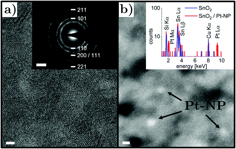 | ||
| Fig. 3 (a) High-resolution transmission electron micrograph of nanocrystalline SnO2 thin film (scale bar 2 nm). Inset: Selected area electron diffraction pattern consistent with polycrystalline rutile structure (scale bar 2 nm−1). (b) High-angle annular dark field image of nanocrystalline SnO2 layer decorated with Pt nanoparticles (scale bar 2 nm). Inset: Energy-dispersive X-ray spectrum of SnO2 film at positions with and without Pt nanoparticle. | ||
However, a more detailed analysis of the atomic-scale structure of ultrasmall Pt nanoparticles after in situ experiments is hampered by the comparatively thick polycrystalline SnO2 support. Consequently, we performed additional experiments using single-crystalline SnO2 nanowires as support for the Pt nanoparticles, serving as model system. In particular, SnO2 nanowires were mechanically transferred to membrane-based heating chips for in situ TEM and subsequently decorated with ultrasmall Pt nanoparticles. TEM imaging was performed before and after in situ heating to 350 °C at an oxygen pressure of 20 mbar at intermediate magnification, and representative results are shown in Fig. 4. Direct comparison of micrographs taken from the same sample position shows that the Pt nanoparticles did not migrate and did not ripen significantly during the heating step. This further confirms that Pt nanoparticles are generally stable on SnO2 at 350 °C, which is an important finding for the interpretation of the chemoresistive sensing results presented above. Our results are in line with previous reports on Pt nanoparticles supported on SiO263 and Al2O3,64,65 which demonstrated that nanoparticle sintering in oxygen-containing atmosphere occurred at 600 °C or above. The average nanoparticle size after thermal oxidation increased by 12% to 1.8 nm, which is attributed to oxidation and morphological changes discussed in the following.
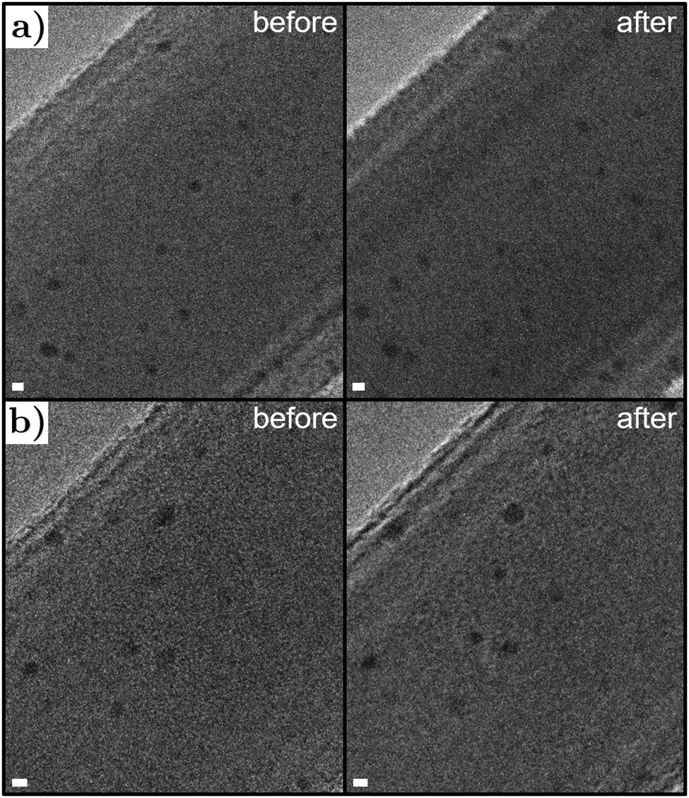 | ||
| Fig. 4 Transmission electron micrographs of Pt nanoparticles supported on single-crystalline SnO2 nanowires before and after in situ heating to 350 °C at an oxygen pressure of 20 mbar for two different nanowires shown in (a) and (b), respectively. All scale bars are 2 nm. | ||
A more detailed investigation of the SnO2 nanowire-supported Pt nanoparticles using high-resolution TEM revealed further aspects of the nanoparticle structure after the in situ heating experiment (Fig. 5). Elongated morphologies related to solid-state wetting were commonly observed and often nanoparticles with disordered crystal structure were found. It is expected that the latter is a result from oxygen incorporation into the nanoparticle lattice. In some cases crystalline planes could be identified providing further evidence for Pt nanoparticle oxidation, as the lattice spacings corresponded to Pt oxide phases rather than metallic Pt. Interestingly, the smallest clusters showed an epitaxial relationship with the SnO2 nanowire support, as can be seen in the right micrograph in Fig. 5. This observation reminds of a recent study demonstrating coherent interfaces between PtO2 nanoparticles and rutile TiO2 supports.66 Similarly, an epitaxial relationship between CuO nanowire supports and Pd nanoparticles after thermal oxidation has been identified, resulting from an interface-driven oxidation mechanism.67 PdO nanoparticles epitaxially aligned to MgO substrates have also been found, but their formation was explained by PdO nanoparticle nucleation and growth enabled by Pd surface diffusion.68,69 Furthermore, epitaxial relationships between nanoparticle and support have been observed for metallic Au70,71 or Rh72 catalysts after treatment at elevated temperatures. In addition to size- and shape-dependent effects,51,73 such strong nanoparticle–support interactions play an important role for nanocatalyst reactivity and thermal stability.66,74
 | ||
| Fig. 5 High-resolution transmission electron micrographs of Pt nanoparticles supported on SnO2 nanowire after in situ heating to 350 °C at an oxygen pressure of 20 mbar (scale bars 2 nm), resulting in nanoparticles with disordered structure (left) and clusters with crystalline structure aligned with respect to the nanowire support (right). | ||
The question arises which Pt oxide phase was formed on the SnO2 support and how this would influence the chemoresistive sensing properties of the SnO2–Pt devices presented above. The nanoparticle lattice spacings observed in our high-resolution TEM analysis were in good agreement with Pt3O4 and β-PtO2 phases. The authors of Nur et al.,66 have argued that, despite the similar crystal structures of their rutile TiO2 support and β-PtO2, the occurrence of the latter is not expected as the synthesis of this phase typically requires high temperatures and pressures. Further, Pt3O4 was formed during the oxidation of Pt nanoparticles supported on MgO75 and on carbon,76 whereas no β-PtO2 was identified. We consequently infer that the Pt nanoparticle functionalization of SnO2 thin films for chemical sensing at elevated temperatures in oxygen atmosphere can most likely be explained by the presence of disordered Pt oxide and Pt3O4 clusters. The observed pronounced oxidation of ultrasmall Pt nanoparticles supported on SnO2 is consistent with X-ray photoelectron spectroscopy studies in literature for clusters in a comparable size range on different substrates.73,76 Note that the presented TEM analysis cannot exclude the possibility of Sn doping of the Pt nanoparticles, but this case is not expected to lead to significant changes in CO reactivity.77
The sensing mechanism of SnO2-based devices in oxygen-containing atmosphere has been explained by oxygen species adsorbed on the SnO2 surface, acting as electron acceptor levels that affect electrical conductivity.78,79 The influence of water vapor has been ascribed to the adsorption of molecular as well as surface hydroxil groups.80 It is expected that the sensing mechanism for the nanocrystalline SnO2 thin film devices presented here is governed by the space charge regions at grain surfaces and interfaces. The CO sensor signal can be attributed to CO reacting with ionosorbed oxygen or direct reactions at the SnO2 surface.79 Humidity interference effects can be understood by a competition between CO and water vapor for reaction sites. In our SnO2–Pt nanomaterial system, we observed minimized humidity interference effects in CO sensing resulting from surface decoration with ultrasmall Pt nanoparticles. Correlating the presented TEM characterization with the sensing measurements, it can be assumed that the observed nanoparticle–support interactions play a central role for the CO sensing mechanism in humid atmosphere. The emergence of oxidized Pt clusters with crystalline structure aligned with respect to the support leads to distinct interfaces and reaction sites, most likely affecting the chemical reactivity. In previous literature, the importance of the three-phase boundary of Pt oxide, SnO2 and the gas phase for CO sensing in humid atmosphere has been highlighted.20 We expect similarities in our case with oxidized ultrasmall Pt clusters influencing the SnO2 layer mainly by chemical sensitization. Minimized humidity interference effects could be attributed to CO reactions at interfacial sites that cause the sensor signal. Moreover, the lowered sensor response of SnO2–Pt devices at higher CO concentrations could be attributed to direct CO oxidation on oxidized Pt clusters without electronic coupling to the sensing layer.20,81 Such a chemical sensitization scenario would be supported by the high catalytic CO oxidation activity of Pt3O482 and by the high reactivity of ultrasmall nanoparticles in general due to a large number of undercoordinated surface sites.83,84 Building on the results presented here, interesting questions and opportunities for future studies emerge, e.g., in situ TEM experiments at higher pressure of the reactive gas atmosphere, morphology and oxidation state changes of ultrasmall Pt nanoparticles induced by exposure to water vapor and CO,85 or the effect of Pt nanoparticle size/shape on humidity interference effects and the overall chemical sensing performance.
4 Conclusions
We have presented the fabrication of size-selected crystalline Pt nanoparticles with an average diameter below 2 nm by magnetron sputtering inert-gas condensation, a solvent-free gas-phase synthesis method for seamless nanoparticle integration with CMOS technology and chemoresistive sensor devices. Minimized humidity interference was observed in the CO sensor response of nanocrystalline SnO2 thin films decorated with Pt nanoparticles and the relevant sensing mechanisms were discussed. In situ heating experiments conducted inside an electron microscope in oxygen atmosphere at conditions relevant for sensor operation showed that the ultrasmall Pt nanoparticles did not migrate or ripen significantly. However, nanoparticle oxidation resulted in structures with pronounced crystal lattice disorder as well as clusters with epitaxial alignment to a crystalline SnO2 support. Our findings show nanoparticle–support interactions in the SnO2–Pt system and provide new insights into the stability of ultrasmall Pt nanoparticles at elevated temperatures in an oxygen environment, which is of significant importance in chemical sensing and catalysis applications.Conflicts of interest
There are no conflicts to declare.Acknowledgements
This work was supported by funding from the OIST Graduate University and has been partly performed within the project “MSP – Multi Sensor Platform for Smart Building Management” (FP7-ICT-2013-10 Collaborative Project, No. 611887).References
- J. Zhang, X. Liu, G. Neri and N. Pinna, Adv. Mater., 2016, 28, 795–831 CrossRef CAS.
- G. Korotcenkov and B. Cho, Sens. Actuators, B, 2017, 244, 182–210 CrossRef CAS.
- D. R. Miller, S. A. Akbar and P. A. Morris, Sens. Actuators, B, 2014, 204, 250–272 CrossRef CAS.
- X. Xue, L. Xing, Y. Chen, S. Shi, Y. Wang and T. Wang, J. Phys. Chem. C, 2008, 112, 12157–12160 CrossRef CAS.
- S. Park, S. An, Y. Mun and C. Lee, ACS Appl. Mater. Interfaces, 2013, 5, 4285–4292 CrossRef CAS.
- O. Lupan, T. Braniste, M. Deng, L. Ghimpu, I. Paulowicz, Y. K. Mishra, L. Kienle, R. Adelung and I. Tiginyanu, Sens. Actuators, B, 2015, 221, 544–555 CrossRef CAS.
- O. Lupan, N. Wolff, V. Postica, T. Braniste, I. Paulowicz, V. Hrkac, Y. K. Mishra, I. Tiginyanu, L. Kienle and R. Adelung, Ceram. Int., 2018, 44, 4859–4867 CrossRef CAS.
- J. Guo, J. Zhang, H. Gong, D. Ju and B. Cao, Sens. Actuators, B, 2016, 226, 266–272 CrossRef CAS.
- G. Tofighi, D. Degler, B. Junker, S. Müller, H. Lichtenberg, W. Wang, U. Weimar, N. Barsan and J.-D. Grunwaldt, Sens. Actuators, B, 2019, 292, 48–56 CrossRef CAS.
- Y.-H. Lin, Y.-C. Hsueh, P.-S. Lee, C.-C. Wang, J. M. Wu, T.-P. Perng and H. C. Shih, J. Mater. Chem., 2011, 21, 10552–10558 RSC.
- G.-J. Sun, S.-W. Choi, S.-H. Jung, A. Katoch and S. S. Kim, Nanotechnology, 2012, 24, 025504 CrossRef.
- J. Shin, S.-J. Choi, I. Lee, D.-Y. Youn, C. O. Park, J.-H. Lee, H. L. Tuller and I.-D. Kim, Adv. Funct. Mater., 2013, 23, 2357–2367 CrossRef CAS.
- X. Liu, N. Chen, B. Han, X. Xiao, G. Chen, I. Djerdj and Y. Wang, Nanoscale, 2015, 7, 14872–14880 RSC.
- X.-T. Yin, W.-D. Zhou, J. Li, Q. Wang, F.-Y. Wu, D. Dastan, D. Wang, H. Garmestani, X.-M. Wang and Ş. Ţălu, J. Alloys Compd., 2019, 805, 229–236 CrossRef CAS.
- M. Dou, M. Hou, D. Liang, W. Lu, Z. Shao and B. Yi, Electrochim. Acta, 2013, 92, 468–473 CrossRef CAS.
- C. Marichy, G. Ercolano, G. Caputo, M. G. Willinger, D. Jones, J. Rozière, N. Pinna and S. Cavaliere, J. Mater. Chem. A, 2016, 4, 969–975 RSC.
- J. Bae, J. Kim, H. Jeong and H. Lee, Catal. Sci. Technol., 2018, 8, 782–789 RSC.
- A. Rabis, T. Binninger, E. Fabbri and T. J. Schmidt, J. Phys. Chem. C, 2018, 122, 4739–4746 CrossRef CAS.
- K. Großmann, S. Wicker, U. Weimar and N. Barsan, Phys. Chem. Chem. Phys., 2013, 15, 19151–19158 RSC.
- D. Degler, H. W. Pereira de Carvalho, K. Kvashnina, J.-D. Grunwaldt, U. Weimar and N. Barsan, RSC Adv., 2016, 6, 28149–28155 RSC.
- G. E. Johnson, R. Colby and J. Laskin, Nanoscale, 2015, 7, 3491–3503 RSC.
- P. Grammatikopoulos, S. Steinhauer, J. Vernieres, V. Singh and M. Sowwan, Adv. Phys. X, 2016, 1, 81–100 CAS.
- Y. Huttel, Gas-Phase Synthesis of Nanoparticles, Wiley, 2017 Search PubMed.
- M. K. Kennedy, F. E. Kruis, H. Fissan, B. R. Mehta, S. Stappert and G. Dumpich, J. Appl. Phys., 2003, 93, 551–560 CrossRef CAS.
- T. Toccoli, S. Capone, L. Guerini, M. Anderle, A. Boschetti, E. Iacob, V. Micheli, P. Siciliano and S. Iannotta, IEEE Sens. J., 2003, 3, 199–205 CrossRef CAS.
- T. Mazza, E. Barborini, I. N. Kholmanov, P. Piseri, G. Bongiorno, S. Vinati, P. Milani, C. Ducati, D. Cattaneo, A. Li Bassi, C. E. Bottani, A. M. Taurino and P. Siciliano, Appl. Phys. Lett., 2005, 87, 103108 CrossRef.
- M. Kennedy, F. Kruis, H. Fissan, H. Nienhaus, A. Lorke and T. Metzger, Sens. Actuators, B, 2005, 108, 62–69 CrossRef CAS.
- A. Lassesson, M. Schulze, J. van Lith and S. A. Brown, Nanotechnology, 2007, 19, 015502 CrossRef.
- M. Khanuja, S. Kala, B. R. Mehta and F. E. Kruis, Nanotechnology, 2008, 20, 015502 CrossRef.
- J. Vernieres, S. Steinhauer, J. Zhao, A. Chapelle, P. Menini, N. Dufour, R. E. Diaz, K. Nordlund, F. Djurabekova, P. Grammatikopoulos and M. Sowwan, Adv. Funct. Mater., 2017, 27, 1605328 CrossRef.
- S. Steinhauer, V. Singh, C. Cassidy, C. Gspan, W. Grogger, M. Sowwan and A. Köck, Nanotechnology, 2015, 26, 175502 CrossRef.
- S. Steinhauer, J. Vernieres, J. Krainer, A. Köck, P. Grammatikopoulos and M. Sowwan, Nanoscale, 2017, 9, 7380–7384 RSC.
- A. Porkovich, Z. Ziadi, P. Kumar, J. Kioseoglou, N. Jian, L. Weng, S. Steinhauer, J. Vernieres, P. Grammatikopoulos and M. Sowwan, ACS Nano, 2019, 13, 12425–12437 CrossRef CAS.
- S. Vajda and M. G. White, ACS Catal., 2015, 5, 7152–7176 CrossRef CAS.
- J. Wang, H.-B. Sun, H.-Y. Pan, Y.-Y. Ding, J.-G. Wan, G.-H. Wang and M. Han, Sens. Actuators, B, 2016, 230, 690–696 CrossRef CAS.
- A. Halder, L. A. Curtiss, A. Fortunelli and S. Vajda, J. Chem. Phys., 2018, 148, 110901 CrossRef.
- A. Datta, A. J. Porkovich, P. Kumar, G. Nikoulis, J. Kioseoglou, T. Sasaki, S. Steinhauer, P. Grammatikopoulos and M. Sowwan, J. Phys. Chem. C, 2019, 123, 26124–26135 CrossRef CAS.
- S. DAddato, L. Gragnaniello, S. Valeri, A. Rota, A. di Bona, F. Spizzo, T. Panozaqi and S. F. Schifano, J. Appl. Phys., 2010, 107, 104318 CrossRef.
- M. Bohra, P. Grammatikopoulos, V. Singh, J. Zhao, E. Toulkeridou, S. Steinhauer, J. Kioseoglou, J.-F. Bobo, K. Nordlund, F. Djurabekova and M. Sowwan, Phys. Rev. Mater., 2017, 1, 066001 CrossRef.
- L. Xing, G. H. ten Brink, B. J. Kooi and G. Palasantzas, J. Appl. Phys., 2017, 121, 024305 CrossRef.
- M. Haro, V. Singh, S. Steinhauer, E. Toulkeridou, P. Grammatikopoulos and M. Sowwan, Adv. Sci., 2017, 4, 1700180 CrossRef.
- S. Kumar, T. Pavloudis, V. Singh, H. Nguyen, S. Steinhauer, C. Pursell, B. Clemens, J. Kioseoglou, P. Grammatikopoulos and M. Sowwan, Adv. Energy Mater., 2018, 8, 1701326 CrossRef.
- E. Brunet, T. Maier, G. Mutinati, S. Steinhauer, A. Köck, C. Gspan and W. Grogger, Sens. Actuators, B, 2012, 165, 110–118 CrossRef CAS.
- M. Siegele, C. Gamauf, A. Nemecek, G. C. Mutinati, S. Steinhauer, A. Köck, J. Kraft, J. Siegert and F. Schrank, 2013 IEEE 11th International New Circuits and Systems Conference (NEWCAS), 2013, pp. 1–4.
- R. Wimmer-Teubenbacher, S. Steinhauer, O. von Sicard, E. Magori, J. Siegert, K. Rohracher, C. Gspan, W. Grogger and A. Köck, Mater. Today: Proc., 2015, 2, 4295–4301 Search PubMed.
- L. Vitos, A. Ruban, H. Skriver and J. Kollár, Surf. Sci., 1998, 411, 186–202 CrossRef CAS.
- L. D. Marks and L. Peng, J. Phys.: Condens. Matter, 2016, 28, 053001 CrossRef CAS.
- J.-G. Mattei, P. Grammatikopoulos, J. Zhao, V. Singh, J. Vernieres, S. Steinhauer, A. Porkovich, E. Danielson, K. Nordlund, F. Djurabekova and M. Sowwan, Chem. Mater., 2019, 31, 2151–2163 CrossRef CAS.
- S. Mostafa, F. Behafarid, J. R. Croy, L. K. Ono, L. Li, J. C. Yang, A. I. Frenkel and B. R. Cuenya, J. Am. Chem. Soc., 2010, 132, 15714–15719 CrossRef CAS.
- Y. Watanabe, X. Wu, H. Hirata and N. Isomura, Catal. Sci. Technol., 2011, 1, 1490–1495 RSC.
- B. R. Cuenya and F. Behafarid, Surf. Sci. Rep., 2015, 70, 135–187 CrossRef.
- N. Barsan and U. Weimar, J. Electroceram., 2001, 7, 143–167 CrossRef CAS.
- S. Wicker, M. Guiltat, U. Weimar, A. Hémeryck and N. Barsan, J. Phys. Chem. C, 2017, 121, 25064–25073 CrossRef CAS.
- G. Mandayo, E. Castaño, F. Gracia, A. Cirera, A. Cornet and J. Morante, Sens. Actuators, B, 2003, 95, 90–96 CrossRef CAS.
- P. Ménini, F. Parret, M. Guerrero, K. Soulantica, L. Erades, A. Maisonnat and B. Chaudret, Sens. Actuators, B, 2004, 103, 111–114 CrossRef.
- N. Ma, K. Suematsu, M. Yuasa, T. Kida and K. Shimanoe, ACS Appl. Mater. Interfaces, 2015, 7, 5863–5869 CrossRef CAS.
- D. Koziej, N. Barsan, K. Shimanoe, N. Yamazoe, J. Szuber and U. Weimar, Sens. Actuators, B, 2006, 118, 98–104 CrossRef CAS.
- H.-R. Kim, A. Haensch, I.-D. Kim, N. Barsan, U. Weimar and J.-H. Lee, Adv. Funct. Mater., 2011, 21, 4456–4463 CrossRef CAS.
- K. Suematsu, M. Sasaki, N. Ma, M. Yuasa and K. Shimanoe, ACS Sens., 2016, 1, 913–920 CrossRef CAS.
- N. Ma, K. Suematsu, M. Yuasa and K. Shimanoe, ACS Appl. Mater. Interfaces, 2015, 7, 15618–15625 CrossRef CAS.
- A. Tischner, T. Maier, C. Stepper and A. Köck, Sens. Actuators, B, 2008, 134, 796–802 CrossRef CAS.
- E. Brunet, PhD thesis, TU Wien, 2014.
- S. B. Simonsen, I. Chorkendorff, S. Dahl, M. Skoglundh, J. Sehested and S. Helveg, J. Catal., 2011, 281, 147–155 CrossRef CAS.
- S. B. Simonsen, I. Chorkendorff, S. Dahl, M. Skoglundh, J. Sehested and S. Helveg, J. Am. Chem. Soc., 2010, 132, 7968–7975 CrossRef CAS.
- S. B. Simonsen, I. Chorkendorff, S. Dahl, M. Skoglundh, K. Meinander, T. N. Jensen, J. V. Lauritsen and S. Helveg, J. Phys. Chem. C, 2012, 116, 5646–5653 CrossRef CAS.
- A. S. M. Nur, E. Funada, S. Kiritoshi, A. Matsumoto, R. Kakei, S. Hinokuma, H. Yoshida and M. Machida, J. Phys. Chem. C, 2018, 122, 662–669 CrossRef CAS.
- S. Steinhauer, J. Zhao, V. Singh, T. Pavloudis, J. Kioseoglou, K. Nordlund, F. Djurabekova, P. Grammatikopoulos and M. Sowwan, Chem. Mater., 2017, 29, 6153–6160 CrossRef CAS.
- N. Kasper, A. Stierle, P. Nolte, Y. Jin-Phillipp, T. Wagner, D. de Oteyza and H. Dosch, Surf. Sci., 2006, 600, 2860–2867 CrossRef CAS.
- P. Nolte, A. Stierle, N. Kasper, N. Y. Jin-Phillipp, H. Reichert, A. Rühm, J. Okasinski, H. Dosch and S. Schöder, Phys. Rev. B: Condens. Matter Mater. Phys., 2008, 77, 115444 CrossRef.
- T. Akita, M. Okumura, K. Tanaka, M. Kohyama and M. Haruta, J. Mater. Sci., 2005, 40, 3101–3106 CrossRef CAS.
- J. González, J. Hernández, M. López-Haro, E. del Río, J. Delgado, A. Hungría, S. Trasobares, S. Bernal, P. Midgley and J. Calvino, Angew. Chem., Int. Ed., 2009, 48, 5313–5315 CrossRef.
- S. Bernal, F. Botana, J. Calvino, G. Cifredo, J. Pérez-Omil and J. Pintado, Catal. Today, 1995, 23, 219–250 CrossRef CAS.
- L. K. Ono, J. R. Croy, H. Heinrich and B. Roldan Cuenya, J. Phys. Chem. C, 2011, 115, 16856–16866 CrossRef CAS.
- L. K. Ono, B. Yuan, H. Heinrich and B. R. Cuenya, J. Phys. Chem. C, 2010, 114, 22119–22133 CrossRef CAS.
- U. Hejral, A. Vlad, P. Nolte and A. Stierle, J. Phys. Chem. C, 2013, 117, 19955–19966 CrossRef CAS.
- R. Banerjee, D. A. Chen, S. Karakalos, M.-L. C. Piedboeuf, N. Job and J. R. Regalbuto, ACS Appl. Nano Mater., 2018, 1, 5876–5884 CrossRef CAS.
- P. Ferrari, L. M. Molina, V. E. Kaydashev, J. A. Alonso, P. Lievens and E. Janssens, Angew. Chem., Int. Ed., 2016, 55, 11059–11063 CrossRef CAS.
- S. Lenaerts, J. Roggen and G. Maes, Spectrochim. Acta, Part A, 1995, 51, 883–894 CrossRef.
- N. Barsan, J. Rebholz and U. Weimar, Sens. Actuators, B, 2015, 207, 455–459 CrossRef CAS.
- N. Yamazoe, J. Fuchigami, M. Kishikawa and T. Seiyama, Surf. Sci., 1979, 86, 335–344 CrossRef CAS.
- P. Kutukov, M. Rumyantseva, V. Krivetskiy, D. Filatova, M. Batuk, J. Hadermann, N. Khmelevsky, A. Aksenenko and A. Gaskov, Nanomaterials, 2018, 8, 917 CrossRef.
- N. Seriani, W. Pompe and L. C. Ciacchi, J. Phys. Chem. B, 2006, 110, 14860–14869 CrossRef CAS.
- E. Altman and R. Gorte, Surf. Sci., 1988, 195, 392–402 CrossRef CAS.
- B. Hammer, O. Nielsen and J. Nørskov, Catal. Lett., 1997, 46, 31–35 CrossRef CAS.
- H. Yoshida, H. Omote and S. Takeda, Nanoscale, 2014, 6, 13113–13118 RSC.
Footnotes |
| † Present address: Department of Applied Physics, KTH Royal Institute of Technology, 106 91 Stockholm, Sweden. E-mail: ssteinh@kth.se |
| ‡ Present address: Department of Physics, Jai Prakash University, Chapra-841301, Bihar, India. |
| This journal is © The Royal Society of Chemistry 2020 |