
 Open Access Article
 This Open Access Article is licensed under a Creative Commons Attribution-Non Commercial 3.0 Unported Licence
Thin film oxide-ion conducting electrolyte for near room temperature applications†
Iñigo
Garbayo‡
 a,
Francesco
Chiabrera
a,
Nerea
Alayo
a,
José
Santiso
b,
Alex
Morata
a and
Albert
Tarancón
*ac
a,
Francesco
Chiabrera
a,
Nerea
Alayo
a,
José
Santiso
b,
Alex
Morata
a and
Albert
Tarancón
*ac
aDepartment of Advanced Materials for Energy Applications, Catalonia Institute for Energy Research (IREC), Jardins de les Dones de Negre 1, 08930 Sant Adrià del Besòs, Barcelona, Spain. E-mail: atarancon@irec.cat
bCatalan Institute of Nanoscience and Nanotechnology (ICN2), CSIC, Barcelona Institute of Science and Technology, Campus UAB, Bellaterra, Barcelona 08193, Spain
cICREA, Passeig Lluís Companys 23, 08010, Barcelona, Spain
First published on 13th September 2019
Abstract
Stabilized bismuth vanadate thin films are presented here as superior oxide ionic conductors, for application in solid state electrochemical devices operating near room temperature. Widely studied in the 90s in bulk form due to their unbeatable ionic conduction, this family of materials was finally discarded due to poor stability above 500 °C. Here, we however unveil the possibility of using Bi4V1.8Cu0.2O10.7 at reduced temperatures in thin film-based devices, where the material keeps its unmatched conduction properties and at the same time shows good stability over a wide oxygen partial pressure range.
The quest for high oxygen ion ceramic conductors has been a very active field of research for decades.1 Aiming to reduce the operating temperature of different oxide ion-driven solid state devices such as solid oxide fuel cells (SOFC) or oxygen sensors, it became necessary to look for alternatives to the state-of-the-art yttria-stabilized zirconia (YSZ) electrolyte material.2–5 The sluggish ion hopping of YSZ typically limited the device operation of bulk systems to e.g. 800 °C in the case of SOFCs,1 or 450 °C for oxygen sensors.6 With the standardization of thin film deposition techniques in the last decades, a significant lowering of the device operating temperature could be attained, simply derived from a substantial reduction of the electrolyte thickness (around 3 orders of magnitude, down to the sub-micrometre range).7 The use of oxide thin films gave rise to new families of integrated solid state MicroElectroMechanical System (MEMS) devices operating at intermediate temperatures, such as thin film SOFCs (TF-SOFCs) for portable power applications,8–10 micro sensors for integrated sensing networks,11,12 or resistive switching devices for data processing.13–15
In the case of TF-SOFCs, the use of hundreds of nanometres thick YSZ electrolytes set a new minimum operating temperature at ca. 450 °C.16–18 When compared to the typical bulk SOFC working temperatures, such a reduction in temperature undoubtedly meant a significant technological breakthrough, attaining quick and low power consuming start-up processes. However, the new temperature range still entailed important restrictions to the cell performance of TF-SOFCs. First, an operating temperature of ∼450 °C was incompatible with state-of-the-art SOFC ceramic electrodes,19 limiting the portfolio of possible electrode materials to inherently instable porous metallic films.8,17,18,20,21 Also, the integration of TF-SOFCs with additional components of the final portable powering device (reformers, post-combustors, or simply electronics)22,23 required a full integration of the system microfabrication in CMOS-compatible Si technology, typically restricted to maximum peak temperatures of 450 °C.24 This limited the broad implementation of TF-SOFC (and, for similar reasons, also gas microsensors) from both a materials and a microfabrication point of view. Further lowering of the operating temperature is therefore still required, for which we are entailed to look for alternative high oxygen conducting electrolyte materials able to operate at reduced temperatures, eventually room temperature.
Low temperature operating oxide ionic conductors find important applications as well in the emerging data storage devices based on transition metal oxide electronic systems, via resistive switching,15 electronic phase transitions25 or voltage controlled ion gating.26 In this sense, it is of particular interest to this work a recent pioneering paper from Yildiz and co-workers, who showed that electrochemically driven phase changes in oxide materials (in particular, VxOy) can be used to trigger metal-insulator transitions and, thus, force large changes in resistivity that could be used for data storage.27 In such system, an ionic conductor is used as gating material, pumping oxygen to (or pulling it out from) the oxide working electrode, forcing the phase change. However, high oxygen mobility needed in the gate limited the operation with solid state materials (YSZ) to a minimum temperature of 300 °C, while room temperature operation was only achieved using ionic liquid gates. Solid state gate materials with superior oxide ionic conduction can therefore open interesting opportunities for the fabrication of electrochemically driven, room temperature operating compact all-solid state memories.
Clearly, the number of alternatives to YSZ is very limited, and all come at a cost. Materials with higher ionic conductivity than YSZ at intermediate temperatures usually suffer from fast degradation under reducing conditions, see e.g. ceria-based electrolytes at T > 600 °C.1 Among the explored alternatives, it is to be highlighted the BIMEVOX family, as the electrolyte material with the highest ionic conductivity at intermediate temperatures ever reported. Firstly described in 1990 by Abraham et al.,28 BIMEVOX presents a layered aurivillius structure consisting of alternating {Bi2O2}2+ and transition metal-doped perovskite {VO3.5□0.5}2− layers, see Fig. 1a. The high presence of disordered oxygen vacancies in the perovskite sheets is the responsible for the high oxygen mobility, which is maximized when stabilizing the tetragonal γ-phase. In the undoped parent compound Bi4V2O11, temperatures below 550 °C lead to the formation of additional monoclinic α and orthorhombic β phases with lower conductivity;29 however, doping with different transition metals has been proved to successfully stabilize the γ-phase down to room temperature. Among the different options, BICUVOX (which stands for the corresponding BIMEVOX doped with Cu and formula Bi4V1.8Cu0.2O10.7, for a typical 10 mol% doping) was shown to present the highest ionic conductivity.28 However, a non-trivial electronic conductivity already at intermediate temperatures (T ∼ 500 °C),30 irreversible phase changes under reducing atmospheres31 and a high thermal expansion coefficient32 drastically hindered the broad application of this material (and the rest of BIMEVOXes) in final pellet-based SOFCs, operating in the intermediate-temperature range. Consequence of this, the material was practically abandoned by the end of that decade, except for its use in oxygen separation membranes.33,34
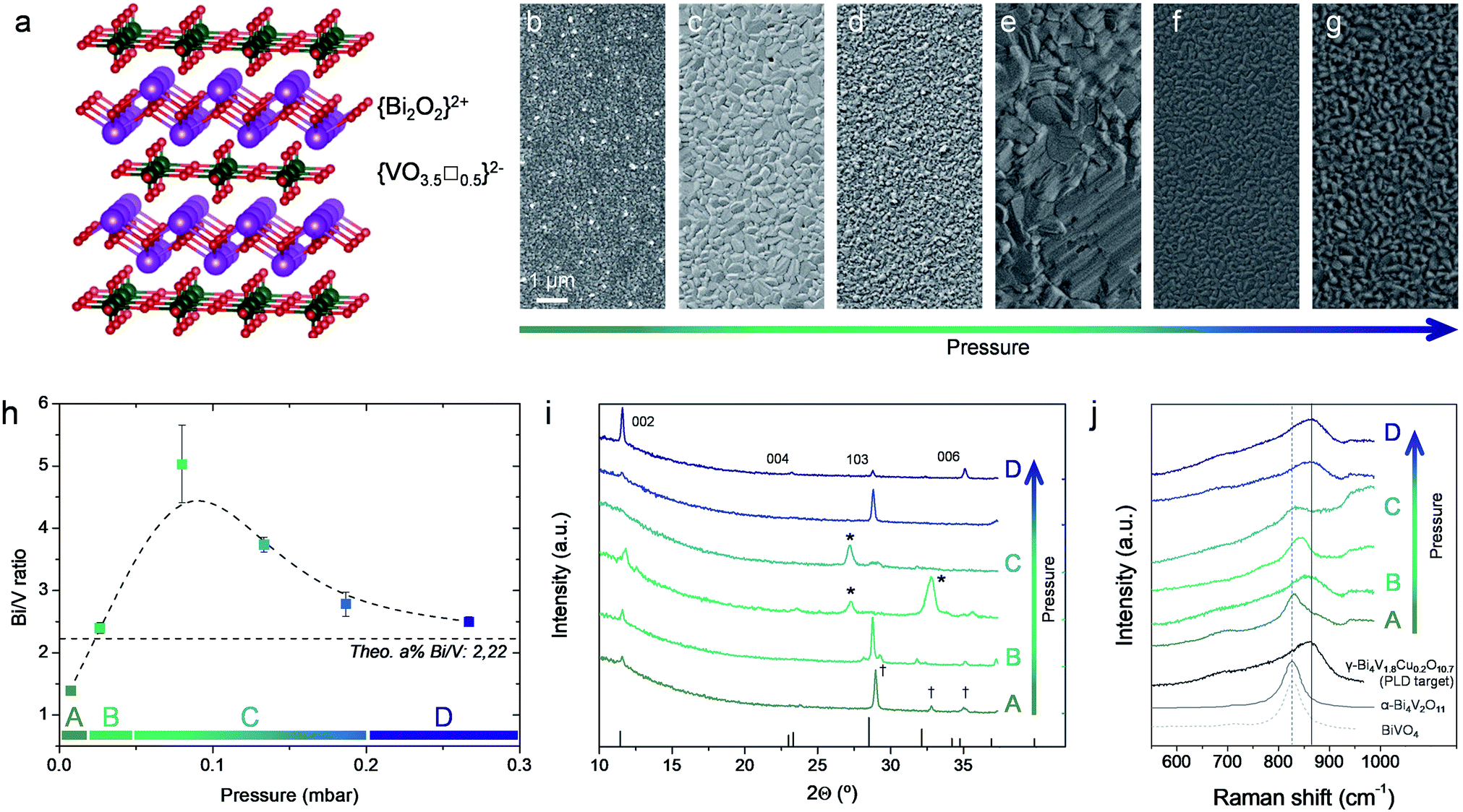 | ||
| Fig. 1 (a) Atomic representation of the γ-Bi4V2O11 aurivillius layered structure (drawings produced by VESTA 3 software).50 (b–g) Top view SEM images of representative films deposited by PLD at different background pressures (p = 0.0067–0.267 mbar) and a constant target-to-substrate distance of 11 cm, on top of Si substrates. (h) Bi/V ratio as a function of deposition pressure. Dashed line is included as guide for the eyes. Four different pressure regions are identified (A–D) (i) X-ray diffractogram obtained for the same BICUVOX film series. Main diffractions of the γ-Bi4V2O11 phase are indicated (ICDD reference code 00-048-0273), as well as the appearance of secondary phases (Bi2O3 *, BiVO4 †) (j) Raman spectra of the BICUVOX film series, plus references for γ-Bi4V1.8Cu0.2O10.7 (measured on the pellet used as PLD target),42 α-Bi4V2O11 (ref. 43) and BiVO4.41 | ||
However, the possibility of fabricating thin film devices, in which the operating temperature can be significantly lowered, opens the door to explore such an outstanding material in a new low temperature range (T ≪ 500 °C), where the chemical instability is expected to be significantly hindered. Despite the promising possibilities for low temperature applications, three decades after the discovery of the high ionic conductivity of BIMEVOX only a few works have dealt with the thin film deposition of this material (thickness <500 nm and low temperature processing),35,36 and a study of its electrochemical performance at this temperature range is still lacking. In this work, we optimized the deposition of BICUVOX thin films by means of Pulsed Laser Deposition (PLD) and we studied its electrochemical performance at T = 50–450 °C. First, we extend previous works and show the tremendous capabilities of PLD for tuning the stoichiometry in this type of films, simply changing the deposition conditions. Then, we present the conduction properties of the optimized BICUVOX films, by measuring its oxygen conductivity as a function of temperature. Noting the layered crystal structure of BICUVOX with oxide ionic diffusion taking place mainly along the {VO3.5□0.5}2− layers, we investigated the anisotropy in the conduction by preparing epitaxial films and measuring their conductivity in orthogonal directions (parallel and perpendicular to the perovskite sheets).
The optimization of PLD deposition of BICUVOX thin films was carried out by preparing a set of polycrystalline films (thickness ranging from 100 to 300 nm) under varying depositing conditions, viz. background oxygen pressure (p) and target-to-substrate distance (d). Other parameters such as deposition temperature and laser fluence were previously optimized for obtaining homogeneous crystalline films and then intentionally set constant, at 600 °C and 0.45 J cm−2 respectively. Thin films were grown from a home-made Bi4V1.8Cu0.2O10.7 target, p was varied from 0.0067 to 0.267 mbar and two target-to-substrate distances were studied, d = 9 and 11 cm (note the longer distances typically used in our large area PLD system compared to “standard” research-scale PLD systems; more details in the Experimental section).37 Dense films were obtained within the whole experimental window of pressures and distances, with considerable variations in the grain size (see representative top view Scanning Electron Microscopy (SEM) images in Fig. 1b–g, for selected background oxygen pressures and d = 11 cm; corresponding images for d = 90 mm can be found in the ESI, Fig. S1†). A stoichiometric analysis of the deposited films was then carried out by Energy-Dispersive X-ray spectroscopy (EDX), Fig. 1h and S2† (specific films were also measured by Wavelength Dispersive Spectroscopy, WDS, confirming the trends). We observed an evolution of the cationic ratio Bi/V as a function of the pressure in analogy with similar representations in the literature involving depositions of heavy vs. light elements (H/L) by PLD.38 We differentiate four different regions; a first region A for low p below 0.0267 mbar, where Bi deficient films are obtained; a region B (p ≈ 0.0267 mbar), where a good stoichiometry is maintained; a region of intermediate pressures C (0.0267 < p < 0.187 mbar) in which an important V deficiency is observed; and a final region D at higher pressures (p > 0.187 mbar), where the film approaches again the target stoichiometry. The observed trend matches well with the expected plume dynamics as a function of the background pressure.38,39 In short, at lower background pressures weak scattering is expected in the laser plume for all the species independently on their size, so the stoichiometry can be well maintained. With increasing pressure, scattering is expected to affect greater to the lighter species (V in our case), giving rise to off-stoichiometric films (light element-deficient). If we keep increasing the background pressure, heavy elements (Bi) start to scatter as well and the plume ends up in a diffusion front in which the correct stoichiometry is recovered, and thus in the films (region D). The presence of a Bi-deficient region at the lowest deposition pressure (region A) is probably related to the high volatility of Bi, which would provoke that at low background pressures, where no collisions are expected in the plume, Bi simply flies away.40 In our case, two pressure regions are clearly identified as preferred for obtaining stoichiometric BICUVOX films, regions B (p = 0.0267 mbar) and D (p > 0.187 mbar).
Importantly, no clear trend could be detected for Cu with the background pressure. However, important differences were detected between the different deposition pressure regions. First, in the low pressure regimes A and B, p = 0.0067–0.0267 mbar, we could identify the presence of homogeneously distributed Cu-rich micrometre-size particles (probably CuO), see top-view SEM image in Fig. S3.† At the same time, in this range it was impossible to detect Cu out of these particles (i.e. in the film), suggesting that Cu could not be successfully integrated in the material and that the films deposited at low p are composed by undoped Bi4V2O11. Opposed to that, for p > 0.0267 mbar (regions C and D), Cu was detected all along the films in the right proportion and no particles were observed. This suggests that in these regimes Cu is indeed successfully incorporated in the BICUVOX structure of the films.
X-Ray Diffraction (XRD) and Raman spectroscopy were carried out in order to analyse the phase evolution through the film series, and the correlation between Bi/V ratio and phase stabilization (Fig. 1i and j). Indeed, the appearance of expectable secondary phases is clearly observed in the films with stoichiometry distant from the targeted one. Analysing the XRD pattern in Fig. 1i, one can observe: (i) the appearance of a Bi-deficient BiVO4 phase at low deposition pressures (p < 0.0267 mbar, region A), probably a mix of clinobisvanite and dreyerite phases,41 and (ii) the presence of Bi2O3 in the V-deficient region C, 0.0267 < p < 0.187 mbar (peaks marked as *). Moreover, even though the desired stoichiometry was measured in films deposited in region B, XRD revealed the presence of additional reflections (see e.g. the triplet peak at 2θ ≈ 28°), presumably due to the aforementioned non-incorporation of Cu in the aurivillius structure and a subsequent non-stabilization of the tetragonal γ-phase. Contrary, at the highest deposition pressures, p > 0.187 mbar, single γ-Bi4V1.8Cu0.2O10.7 phase could only be detected.
Similar conclusions can be drawn by Raman spectroscopy, Fig. 1j. In fact, it is to be highlighted the goodness of Raman spectroscopy for identifying phase formation in the Bi4V2O11 family, since a clear shift in wavenumber, from ∼860 cm−1 to ∼830 cm−1, happens when moving from the tetragonal γ-phase to monoclinic α-phase (see difference between the γ-Bi4V1.8Cu0.2O10.7, measured in the pellet used as PLD target and perfectly matching previous reports,42 and the α-Bi4V2O11 from ref. 43). This way, we could clearly identify the presence of the desired tetragonal phase in the films deposited at high pressure, region D (p > 0.187 mbar). Meanwhile, α-Bi4V2O11 was detected in the intermediate pressures, and BiVO4 was presumably measured at the lowest pressure tested (note here that similar spectra have been reported for both α-Bi4V2O11 and BiVO4, making impossible to differentiate them by this technique). Surprisingly, at p ≈ 0.0267 mbar Raman spectroscopy also shows the stabilization of the γ-phase, even though Cu is apparently not well incorporated in the structure. Still, we can conclude that XRD and Raman results fully support, from a structural point of view, the stoichiometric evolution previously observed, and suggest the need of high background pressures of p > 0.187 mbar for the stabilization of the aurivillius BICUVOX γ-phase.
Based on this, we additionally prepared epitaxial BICUVOX films grown on (001)-oriented SrTiO3 substrates (undoped – STO and doped with 1.0 at% Nb – Nb:STO), at the optimum deposition pressure of p = 0.267 mbar. Fig. 2a shows a representative XRD pattern of a 36 nm-thick BICUVOX film deposited on Nb:STO (see section S2 of the ESI† for the corresponding measurements on undoped STO). The appearance of a set of reflections corresponding to the (00L) family of planes reveals a perfect epitaxial growth of the tetragonal aurivillius γ-phase, (00L)-oriented in the c-axis (more details in section S2†). The φ-scan presented in the inset of Fig. 2a confirms a cube-on-cube growth of the tetragonal BICUVOX on top of Nb:STO with perfect match of the (100) planes of both materials, see schematics in Fig. 2c. Note the almost identical in-plane lattice parameter of BICUVOX, aBICUVOX = 3.907 Å,28 as compared to the cubic STO, aSTO = 3.905 Å, meaning a lattice mismatch of only +0.05%. The epitaxy was confirmed by performing high resolution XRD reciprocal space maps (RSM), Fig. 2b and S4.† The figure shows the coexisting reflections (−103) of the Nb:STO and (−1011) of the BICUVOX, revealing a perfect in-plane matching thanks to the very similar in-plane lattice parameters.
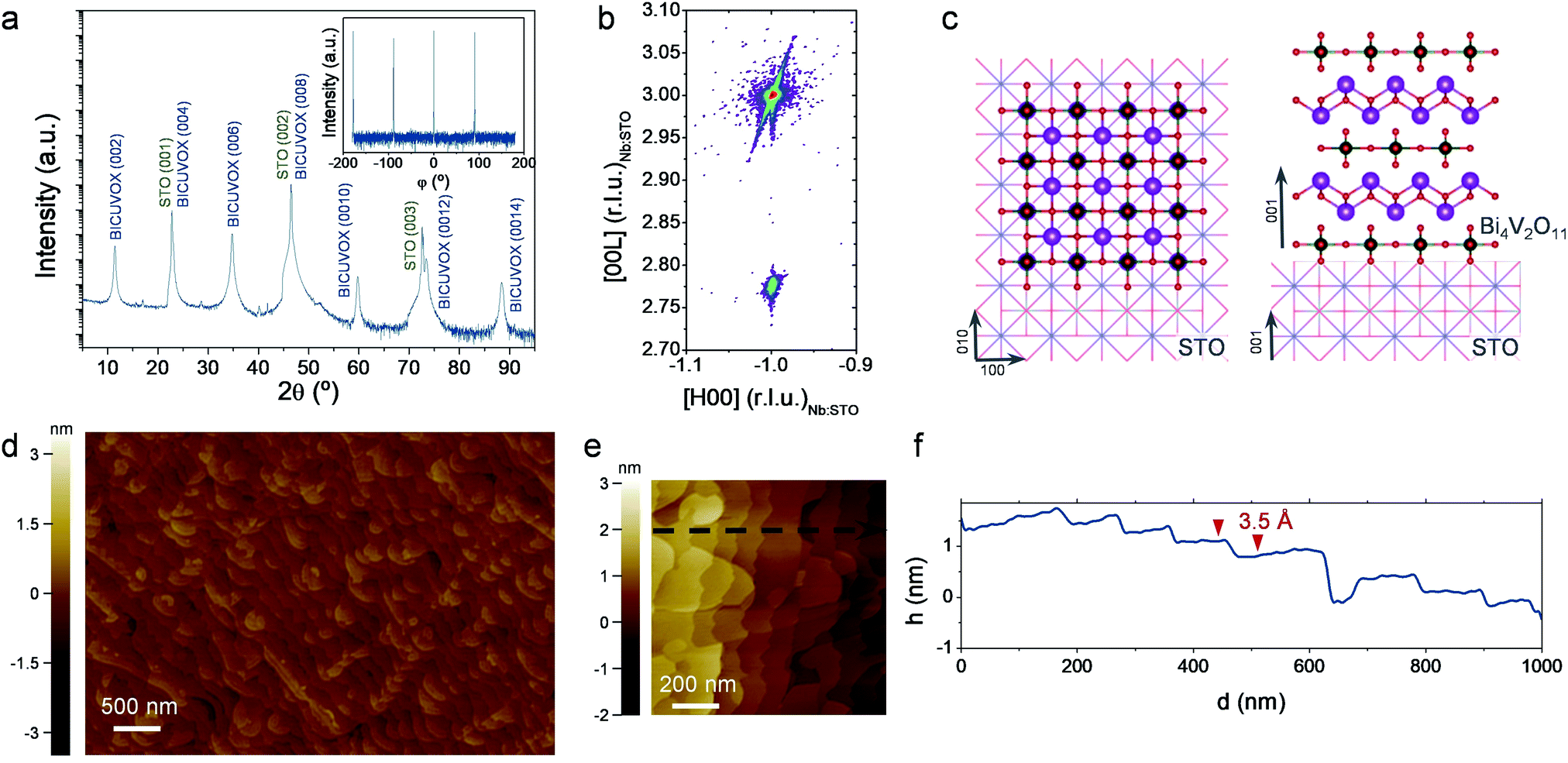 | ||
| Fig. 2 (a and b) X-ray diffraction patterns of a 36 nm thick BICUVOX film deposited on Nb-doped SrTiO3. (a) Out-of-plane θ–2θ X-ray diffraction pattern, where the set of peaks corresponding to the 00L reflections is visible. A φ scan around the (−103) reflection of SrTiO3 is also included in the inset, showing a 4-fold symmetry corresponding to a single in-plane orientation (100) BICUVOX/(100) SrTiO3. (b) Shows the in-plane Reciprocal Space Map around the −103 reflection peak of the Nb-doped SrTiO3 substrate. (c) Schematic representations of the epitaxial growth of γ-Bi4V2O11 on top of 001-oriented SrTiO3 single crystals, top and cross-sectional views. (d and e) AFM images of an epitaxial BICUVOX film grown on top of Nb-doped SrTiO3, with two different magnifications. (f) Height profile corresponding to the black dashed arrow shown in figure (e). The average step height is shown as well (only single step terraces are considered for the average calculation). | ||
Furthermore, the quality of the films was analysed by top-view non-contact AFM images, Fig. 2d and e. The images showed a clear formation of terraces, typical of layer by layer growth,35 and a complete absence of significant defects or particulates in the top surface. The height profile obtained along the top surface (black dashed arrow in Fig. 2e) revealed very small steps of ∼3.5 Å, see Fig. 2f. These steps are clearly smaller than the out-of-plane lattice parameter (cBICUVOX = 15.44 Å, as calculated from the out-of-plane XRD pattern and matching previous literature).28 We speculate that these steps correspond to single {Bi2O2}2+ or {VO3.5□0.5}2− sub-layers, 4 every unit cell, thus matching the obtained average value. In conclusion, we were able to grow high quality epitaxial BICUVOX films in two functional substrates, one dielectric (STO), one conductive (Nb:STO), ideal for further electrochemical analysis.
Ionic conductivity in the whole set of BICUVOX films was investigated by means of Electrochemical Impedance Analysis (EIS). Epitaxial (on STO-based substrates) and polycrystalline (on Si3N4/SiO2/Si substrates) films were measured in a temperature range from 50 to 450 °C, under ambient conditions (corresponding Nyquist plots can be found in the ESI, Fig. S6†). First, the effect of film off-stoichiometry and presence of secondary phases (see Fig. 1) on the conduction properties of the polycrystalline films was confirmed, correlating the stabilization of the fast conducting and stable γ-phase with the obtaining of highest (and stable) conductivity (see section S3 in the ESI†). We then focus on the analysis of the polycrystalline vs. epitaxial films, all deposited at the optimum pressure range, p = 0.267 mbar. Fig. 3a presents the Arrhenius representation of the conductivity evolution with temperature, for one polycrystalline film and two epitaxial BICUVOX films measured at two different configurations, viz. in-plane (on STO) and cross-plane (on Nb:STO), using top Au electrodes (further details on the different measuring configurations can be found in section S3†). The obtained results are compared with reference bulk polycrystalline BICUVOX, as well as single crystal BICUVOX in two directions (parallel and perpendicular to the (100)BICUVOX planes) and, finally, YSZ and Gd-doped CeO2 (CGO) thin film conductivity.16,47–49
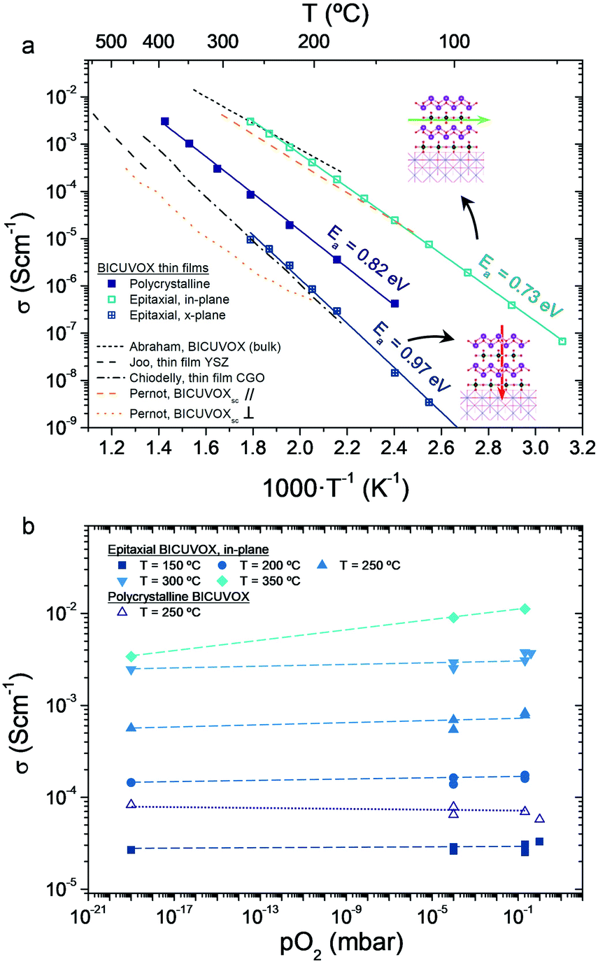 | ||
| Fig. 3 (a) Arrhenius representation of the evolution of ionic conductivity for different BICUVOX (polycrystalline, epitaxial) films with temperature, all deposited at p = 0.267 mbar. References for bulk polycrystalline BICUVOX,28 single crystal BICUVOX (parallel and perpendicular to the (100)BICUVOX planes),48 YSZ thin film16,46 and CGO thin film44,45 are included for comparison. Inset schematics show the direction of oxygen mobility in the two measuring configurations, for the epitaxial films. Activation energies (Ea) are also indicated for the measured films. (b) pO2 dependence of BICUVOX in-plane conductivity, measured in an epitaxial film at different temperatures (T = 150–350 °C) and in a polycrystalline sample at T = 250 °C. Oxygen partial pressure is measured by an oxygen sensor at the outlet of the gases. Dashed lines are included as guide for the eyes. | ||
Although significant differences are found among the different films, all present an improvement in terms of ionic conduction vs. state-of-the-art YSZ and CGO, especially when reducing temperature (due to the lower activation energies, Ea). The highest conductivity is clearly obtained in the epitaxial BICUVOX film when measuring in-plane, followed by the polycrystalline film and, finally, the epitaxial measured cross-plane. As for the activation energies, one single mechanism could be observed for the whole range of measuring temperatures, with slightly higher Ea for the cross-plane than for the in-plane conduction.
The measured in-plane conductivity for the epitaxial film goes in line with literature values for bulk BICUVOX, confirming the outstanding oxide ionic conductivity of this material in thin film form (the slightly higher Ea values could be related to the plausible presence of structural defects in the films or small off-stoichiometries). The expected anisotropy in the conduction, depending on the oxygen hopping direction, is also clearly observed in the measured films, with more than two orders of magnitude higher in-plane conductivity than cross-plane. Similar anisotropy was previously reported in single crystal BICUVOX and matches well with our XRD results, Fig. 2, since enhanced oxygen mobility in BICUVOX is known to happen along the {VO3.5□0.5}2− sub-layers, i.e. in the direction parallel to the substrate surface (in-plane), and hindered when crossing the {Bi2O2}2+ sub-layers, i.e. in the (001)BICUVOX direction, across the film.48,50 Interestingly, the polycrystalline film presents both an intermediate conductivity and activation energy, probably derived from the random orientation of the grains and the presence of grain boundaries.
Notably, these results position the prepared epitaxial BICUVOX films as the thin film material with highest (in-plane) ionic conductivity ever reported for low temperature applications (T < 300 °C), with important implications for their application in advanced thin film-based devices. However, apart from the outstanding oxide ionic conductivity, low temperature operation with BICUVOX films also requires high stability in a wide range of pO2, from oxidizing to highly reducing atmospheres (especially for applications in powering devices). Indeed, as commented before, this has been the main drawback of BICUVOX hindering its use as electrolyte material at higher temperatures in the past. We therefore studied the stability vs. pO2 of the utmost performing BICUVOX epitaxial film in its new operating temperature range, T < 300 °C. Fig. 3b presents the in-plane conductivity measured by EIS at different temperatures, from 150 °C to 350 °C, and oxygen partial pressures, from pO2 = 0.21 bar (synthetic air) to pO2 = 10−19 bar (5 vol% H2 in Ar). For temperatures below 300 °C, the figure shows great stability (flat profiles) within the whole range of pO2 (from oxidizing to highly reducing conditions), proving the effectiveness of the material to be used in thin film-based low temperature operating devices. The maximum operating temperature for epitaxial BICUVOX is set in this study at T = 350 °C, since a clear effect on the conductivity is observed there when reducing pO2. It is important to note, though, that the observed trend at this temperature matches well with an unexpected p-type conduction behaviour. The appearance of this conduction comportment at this temperature requires attention and will be a matter of discussion in further works.
Finally, we also analysed the stability vs. pO2 of the BICUVOX polycrystalline films. Although not as outstanding as the in-plane conductivity measured in the epitaxial films (between one and two orders of magnitude lower), the polycrystalline BICUVOX already represents an important reduction of ∼150 °C and ∼100 °C vs. YSZ and CGO respectively, with a potential operating temperature below 300 °C. As shown in Fig. 3b stability tests (open symbols), negligible conductivity changes vs. pO2 were detected also in the polycrystalline films at T = 250 °C, thus proving the viability of the material in the low temperature operating range. Taking into account that for certain applications this microstructure might be significantly easier to implement than an epitaxial film (e.g. in the already existing TF-SOFC systems), polycrystalline BICUVOX are expected to play a crucial role in future low temperature devices too.
Conclusions
Epitaxial and polycrystalline BICUVOX thin films are presented here as superior oxygen conducting electrolyte materials, for their application in thin film-based low temperature operating electrochemical solid state devices. The highest conductivity was observed in the epitaxial BICUVOX films when measuring parallel to the {VO3.5□0.5}2− planes, matching that previously reported for bulk BICUVOX and thus surpassing any other thin film oxide ion conducting material ever reported at the low temperature operating range (T < 300 °C). At the same time, polycrystalline BICUVOX films also showed an outstanding performance, with forecasted operating temperature below 300 °C. The high ionic conductivity, added to the high stability vs. pO2 proved in this low temperature range, anticipates the potential use of BICUVOX down to room temperature in a new family of non-heated solid state electrochemical systems. Importantly, the use of this material opens up amazing possibilities for the fabrication of solid state devices fully integrated in CMOS processing technologies and with possible encapsulation in plastics.Experimental section
Thin film deposition by PLD
BICUVOX thin films were deposited by large-area pulsed laser deposition (PLD5000, PVD Products) under different background O2 pressures (0.0067 to 0.267 mbar) and target-to-substrate distances (9 to 11 cm), from a home-made Bi4V1.8Cu0.2O10.7 pellet target. For the fabrication of the target, Bi4V1.8Cu0.2O10.7 powder was first synthesized in-house by solid state synthesis, from the basic oxide precursors (Bi2O3, V2O5 and CuO) mixed in the right stoichiometric proportion. Then, a 3′′ pellet was pressed by uniaxial pressing and sintered under ambient air at 850 °C for 6 h. All BICUVOX films were deposited at a substrate temperature of 600 °C, and on various types of substrates, including single crystal Si (100-oriented), sapphire, fused silica, and Si (100) coated with Si3N4 (300 nm)/SiO2 (100 nm) dielectric bilayer. For the growth of epitaxial BICUVOX films, SrTiO3 (STO) and Nb-doped STO (Nb:STO) substrates (Crystal GmbH, Germany) were used, for in-plane and cross-plane electrochemical analysis, respectively.Thin film structural and compositional characterization
Long range crystalline structure of the deposited films was characterized by X-ray Diffraction (XRD, Bruker D8 Advanced), under a typical θ/2θ Bragg–Brentano geometry. For the epitaxial films, a four-angle diffractometer (X'Pert MRD-Panalytical) was used with a Cu Kα radiation source. Additionally, the near range order was analysed by Raman spectroscopy (Horiba Jobin Ybon iHR320). For the Raman measurements, green laser (λ = 532 nm) was utilized under no light polarization. Thin films microstructure was studied by Scanning Electron Microscopy top view imaging (SEM, ZEISS AURIGA). SEM-coupled Energy-Dispersive X-ray spectroscopy (EDX) was used for the elemental distribution analysis. Errors in the EDX analysis were estimated by calculating the standard deviation from multiple measurements in several samples. Non-contact Atomic Force Microscopy (AFM, XE 100 Park System Corp.) was additionally used for top view imaging of the epitaxial BICUVOX films.Thin film electrochemical measurements
Electrochemical Impedance Spectroscopy (EIS) was used for measuring the electrical properties of the BICUVOX films, with the help of a Novocontrol Alpha-A Impedance analyser. 100 nm-thick top Au blocking interdigitated (for in-plane measurements) and circular (for cross-plane measurements) electrodes with varying sizes were first defined by photolithography and then deposited by e-beam evaporation (OERLIKON UNIVEX 450B). Impedance was measured in a frequency range of 1 MHz–0.1 Hz applying an AC voltage of 50 mV, in a temperature-controlled Linkam probe station, from 50 to 450 °C. Results were analysed with a ZView software and fitting was carried out applying equivalent circuit modelling.Conflicts of interest
There are no conflicts to declare.Acknowledgements
The research was supported by the Generalitat de Catalunya-AGAUR (2017 SGR 1421). This project has received funding from the European research Council (ERC) under the European Union's Horizon 2020 research and innovation programme (ULTRASOFC, Grant Agreement number: 681146).References
- J. B. Goodenough, Annu. Rev. Mater. Res., 2003, 33, 91–128 CrossRef CAS.
- S. C. Singhal and K. Kendall, High Temperature Solid Oxide Fuel Cells: Fundamentals, Design, and Applications, Elsevier Advanced Technology, 2003 Search PubMed.
- A. Tarancón, Energies, 2009, 2, 1130–1150 CrossRef.
- Z. Gao, L. V. Mogni, E. C. Miller, J. G. Railsback, S. A. Barnett, J. B. Goodenough, K. Huang, A. Tarancon, H. Yokokawa, J. Janek, Y. Shao-Horn, J. H. Lang, J. H. Yang, T. McColm, R. Trezona, A. Selcuk, M. Schmidt and L. Verdugo, Energy Environ. Sci., 2016, 9, 1602–1644 RSC.
- B. Singh, S. Ghosh, S. Aich and B. Roy, J. Power Sources, 2017, 339, 103–135 CrossRef CAS.
- A. M. Azad, S. A. Akbar, S. G. Mhaisalkar, L. D. Birkefeld and K. S. Goto, J. Electrochem. Soc., 1992, 139, 3690 CrossRef CAS.
- D. Beckel, A. Bieberle-Hütter, A. Harvey, A. Infortuna, U. P. Muecke, M. Prestat, J. L. M. Rupp and L. J. Gauckler, J. Power Sources, 2007, 173, 325–345 CrossRef CAS.
- M. Tsuchiya, B.-K. Lai and S. Ramanathan, Nat. Nanotechnol., 2011, 6, 282–286 CrossRef CAS PubMed.
- A. Evans, A. Bieberle-Hütter, J. L. M. Rupp and L. J. Gauckler, J. Power Sources, 2009, 194, 119–129 CrossRef CAS.
- I. Garbayo, D. Pla, A. Morata, L. Fonseca, N. Sabaté and A. Tarancón, Energy Environ. Sci., 2014, 7, 3617–3629 RSC.
- B.-U. Moon, J.-M. Lee, C.-H. Shim, M.-B. Lee, J.-H. Lee, D.-D. Lee and J.-H. Lee, Sens. Actuators, B, 2005, 108, 271–277 CrossRef CAS.
- S. Yu, Q. Wu, M. Tabib-Azar and C.-C. Liu, Sens. Actuators, B, 2002, 85, 212–218 CrossRef CAS.
- R. Waser and M. Aono, Nat. Mater., 2007, 6, 833–840 CrossRef CAS PubMed.
- D. Ielmini, Semicond. Sci. Technol., 2016, 31, 063002 CrossRef.
- C. Bäumer and R. Dittmann, in Metal Oxide-Based Thin Film Structures, Elsevier, 2018, pp. 489–522 Search PubMed.
- I. Garbayo, A. Tarancón, J. Santiso, F. Peiró, E. Alarcón-LLadó, A. Cavallaro, I. Gràcia, C. Cané and N. Sabaté, Solid State Ionics, 2010, 181, 322–331 CrossRef CAS.
- K. Kerman, B.-K. Lai and S. Ramanathan, J. Power Sources, 2011, 196, 2608–2614 CrossRef CAS.
- J. An, Y.-B. Kim, J. Park, T. M. Gür and F. B. Prinz, Nano Lett., 2013, 13, 4551–4555 CrossRef CAS PubMed.
- I. Garbayo, V. Esposito, S. Sanna, A. Morata, D. Pla, L. Fonseca, N. Sabaté and A. Tarancón, J. Power Sources, 2014, 248, 1042–1049 CrossRef CAS.
- K. Kerman, B.-K. Lai and S. Ramanathan, J. Power Sources, 2012, 202, 120–125 CrossRef CAS.
- Y. Takagi, S. Adam and S. Ramanathan, J. Power Sources, 2012, 217, 543–553 CrossRef CAS.
- D. Pla, A. Sánchez-González, I. Garbayo, M. Salleras, A. Morata and A. Tarancón, J. Power Sources, 2015, 293, 264–273 CrossRef CAS.
- B. Scherrer, A. Evans, A. J. Santis-Alvarez, B. Jiang, J. Martynczuk, H. Galinski, M. Nabavi, M. Prestat, R. Tölke, A. Bieberle-Hütter, D. Poulikakos, P. Muralt, P. Niedermann, A. Dommann, T. Maeder, P. Heeb, V. Straessle, C. Muller and L. J. Gauckler, J. Power Sources, 2014, 258, 434–440 CrossRef CAS.
- S. Sedky, A. Witvrouw, H. Bender and K. Baert, IEEE Trans. Electron Devices, 2001, 48, 377–385 CrossRef CAS.
- N. Shukla, A. V. Thathachary, A. Agrawal, H. Paik, A. Aziz, D. G. Schlom, S. K. Gupta, R. Engel-Herbert and S. Datta, Nat. Commun., 2015, 6, 7812 CrossRef CAS.
- A. L. Krick and S. J. May, APL Mater., 2017, 5, 042504 CrossRef.
- Q. Lu, S. R. Bishop, D. Lee, S. Lee, H. Bluhm, H. L. Tuller, H. N. Lee and B. Yildiz, Adv. Funct. Mater., 2018, 28, 1803024 CrossRef.
- F. Abraham, J. C. Boivin, G. Mairesse and G. Nowogrocki, Solid State Ionics, 1990, 40–41, 934–937 CrossRef CAS.
- F. Abraham, M. F. Debreuille-Gresse, G. Mairesse and G. Nowogrocki, Solid State Ionics, 1988, 28–30, 529–532 CrossRef.
- T. Iharada, A. Hammouche, J. Fouletier, M. Kleitz, J. C. Boivin and G. Mairesse, Solid State Ionics, 1991, 48, 257–265 CrossRef CAS.
- M. Guillodo, J. Fouletier, L. Dessemond and P. Del Gallo, Electrochim. Acta, 2002, 47, 2809–2815 CrossRef CAS.
- M. C. Steil, F. Ratajczak, E. Capoen, C. Pirovano, R. N. Vannier and G. Mairesse, Solid State Ionics, 2005, 176, 2305–2312 CrossRef CAS.
- J. C. Boivin, C. Pirovano, G. Nowogrocki, G. Mairesse, P. Labrune and G. Lagrange, Solid State Ionics, 1998, 113–115, 639–651 CrossRef CAS.
- M. H. Paydar, A. M. Hadian and G. Fafilek, J. Mater. Sci., 2006, 41, 1953–1957 CrossRef CAS.
- C. Sant and J. P. Contour, J. Cryst. Growth, 1995, 153, 63–67 CrossRef CAS.
- K. Trzciński, J. Gasiorowski, A. Borowska-Centkowska, M. Szkoda, M. Sawczak, K. Hingerl, D. R. T. Zahn and A. Lisowska-Oleksiak, Thin Solid Films, 2017, 638, 251–257 CrossRef.
- A. Ojeda-G-P, C. W. Schneider, M. Döbeli, T. Lippert and A. Wokaun, J. Appl. Phys., 2017, 121, 135306 CrossRef.
- S. Amoruso, in Metal Oxide-Based Thin Film Structures, Elsevier, 2018, pp. 133–160 Search PubMed.
- A. Ojeda-G-P, C. W. Schneider, M. Döbeli, T. Lippert and A. Wokaun, Appl. Surf. Sci., 2016, 389, 126–134 CrossRef CAS.
- S. Havelia, S. Wang, M. Skowronski and P. A. Salvador, J. Appl. Phys., 2009, 106, 123509 CrossRef.
- R. L. Frost, D. A. Henry, M. L. Weier and W. Martens, J. Raman Spectrosc., 2006, 37, 722–732 CrossRef CAS.
- R. Bacewicz and P. Kurek, Solid State Ionics, 2000, 127, 151–156 CrossRef CAS.
- S. Kumar and P. D. Sahare, Nano, 2012, 08, 1350007 CrossRef.
- G. Chiodelli, L. Malavasi, V. Massarotti, P. Mustarelli and E. Quartarone, Solid State Ionics, 2005, 176, 1505–1512 CrossRef CAS.
- J. L. M. Rupp and L. J. Gauckler, Solid State Ionics, 2006, 177, 2513–2518 CrossRef CAS.
- J. H. Joo and G. M. Choi, Solid State Ionics, 2006, 177, 1053–1057 CrossRef CAS.
- P. Kurek, J. R. Dygas and M. W. Breiter, Solid State Phenom., 1994, 39–40, 247–250 CAS.
- E. Pernot, M. Anne, M. Bacmann, P. Strobel, J. Fouletier, R. N. Vannier, G. Mairesse, F. Abraham and G. Nowogrocki, Solid State Ionics, 1994, 70–71, 259–263 CrossRef CAS.
- N. P. Brandon, S. Skinner and B. C. H. Steele, Annu. Rev. Mater. Res., 2003, 33, 183–213 CrossRef CAS.
- K. Momma and F. Izumi, J. Appl. Crystallogr., 2011, 44, 1272–1276 CrossRef CAS.
Footnotes |
| † Electronic supplementary information (ESI) available: Supplementary images S1–S8 distributed in five supplementary sections (S1 to S5). See DOI: 10.1039/c9ta07632h |
| ‡ Present address: CIC Energigune, Parque Tecnológico de Álava, 01510 Vitoria-Gasteiz, Spain. |
| This journal is © The Royal Society of Chemistry 2019 |