
 Open Access Article
 This Open Access Article is licensed under a Creative Commons Attribution-Non Commercial 3.0 Unported Licence
Large area efficient interface layer free monolithic perovskite/homo-junction-silicon tandem solar cell with over 20% efficiency†
Jianghui
Zheng‡
 *a,
Cho Fai Jonathan
Lau‡
a,
Hamid
Mehrvarz‡
a,
Fa-Jun
Ma
a,
Yajie
Jiang
a,
Xiaofan
Deng
a,
Anastasia
Soeriyadi
a,
Jincheol
Kim
a,
Meng
Zhang
a,
Long
Hu
a,
Xin
Cui
a,
Da Seul
Lee
a,
Jueming
Bing
a,
Yongyoon
Cho
a,
Chao
Chen
b,
Martin A.
Green
a,
Shujuan
Huang
a and
Anita W. Y.
Ho-Baillie
*a
*a,
Cho Fai Jonathan
Lau‡
a,
Hamid
Mehrvarz‡
a,
Fa-Jun
Ma
a,
Yajie
Jiang
a,
Xiaofan
Deng
a,
Anastasia
Soeriyadi
a,
Jincheol
Kim
a,
Meng
Zhang
a,
Long
Hu
a,
Xin
Cui
a,
Da Seul
Lee
a,
Jueming
Bing
a,
Yongyoon
Cho
a,
Chao
Chen
b,
Martin A.
Green
a,
Shujuan
Huang
a and
Anita W. Y.
Ho-Baillie
*a
aAustralian Centre for Advanced Photovoltaics, School of Photovoltaic and Renewable Energy Engineering, University of New South Wales (UNSW), Sydney 2052, Australia. E-mail: a.ho-baillie@unsw.edu.au; jh.zheng@unsw.edu.au
bCollege of Energy, Xiamen University, Xiamen, 361005, China
First published on 25th June 2018
Abstract
Monolithic perovskite/silicon tandem solar cells show great promise for further efficiency enhancement for current silicon photovoltaic technology. In general, an interface (tunnelling or recombination) layer is usually required for electrical contact between the top and the bottom cells, which incurs higher fabrication costs and parasitic absorption. Most of the monolithic perovskite/Si tandem cells demonstrated use a hetero-junction silicon (Si) solar cell as the bottom cell, on small areas only. This work is the first to successfully integrate a low temperature processed (≤150 °C) planar CH3NH3PbI3 perovskite solar cell on a homo-junction silicon solar cell to achieve a monolithic tandem without the use of an additional interface layer on large areas (4 and 16 cm2). Solution processed SnO2 has been effective in providing dual functions in the monolithic tandem, serving as an ETL for the perovskite cell and as a recombination contact with the n-type silicon homo-junction solar cell that has a boron doped p-type (p++) front emitter. The SnO2/p++ Si interface is characterised in this work and the dominant transport mechanism is simulated using Sentaurus technology computer-aided design (TCAD) modelling. The champion device on 4 cm2 achieves a power conversion efficiency (PCE) of 21.0% under reverse-scanning with a VOC of 1.68 V, a JSC of 16.1 mA cm−2 and a high FF of 78% yielding a steady-state efficiency of 20.5%. As our monolithic tandem device does not rely on the SnO2 for lateral conduction, which is managed by the p++ emitter, up scaling to large areas becomes relatively straightforward. On a large area of 16 cm2, a reverse scan PCE of 17.6% and a steady-state PCE of 17.1% are achieved. To our knowledge, these are the most efficient perovskite/homo-junction-silicon tandem solar cells that are larger than 1 cm2. Most importantly, our results demonstrate for the first time that monolithic perovskite/silicon tandem solar cells can be achieved with excellent performance without the need for an additional interface layer. This work is relevant to the commercialisation of efficient large-area perovskite/homo-junction silicon tandem solar cells.
Broader contextA simple approach for integrating a perovskite solar cell monolithically onto a Si solar cell is reported here. The first advantage of this approach is that it does not require additional fabrication of an additional interface layer between the perovskite and Si cell. The second advantage of this approach is that it is compatible with a homo-junction p–n Si solar cell, which is a common Si solar cell structure for commercial cells. The third advantage is that the entire sequence for the planar perovskite cell fabrication is done at low temperatures, minimising damage to the bottom Si solar cell. The fourth advantage is that the SnO2 electron transport layer of the perovskite top cell also serves as a recombination contact with the silicon bottom cell. Finally, this monolithic tandem approach does not rely on the SnO2 for lateral conduction, which is managed by the p++ emitter, making upscaling to large areas relatively straightforward. The SnO2/p++ interface is characterised and modelled in this work to explain the dominant transport mechanism. Pathways to improve the optical performance of the tandem are simulated and demonstrated. The outlook to achieve a 30% efficient monolithic perovskite/silicon tandem is also presented. With regards to cell demonstrations, a stabilized efficiency at 20.5% has been achieved on 4 cm2 and a stabilized efficiency at 17.1% is achieved on an even larger area of 16 cm2. To our knowledge, these are the most efficient monolithic perovskite/silicon-homojunction tandem solar cells larger than 1 cm2 reported. This unique tandem design presented in this work paves a way for commercially relevant, low cost, efficient, large-area perovskite/homo-junction Si tandems. |
1. Introduction
Organic–inorganic hybrid perovskite solar cells (PSCs) have superior optical absorption and their ease of fabrication has attracted great attention resulting in a rapid improvement in power conversion efficiency (PCE) from 3.8% to certified 22.7% in a few years.1–3 In particular, organic–inorganic hybrid perovskites are suitable for tandem solar cells due to a wide allowable bandgap range achievable via compositional engineering.4 The integration of perovskite and Si solar cells for double junction tandems can overcome the Shockley–Queisser limit for single junction solar cells at ∼33%5 to above 40%.6Recently, many demonstrations of perovskite/silicon tandem solar cells have been reported.7–23 A 4-terminal tandem involves mechanical stacking of a semitransparent perovskite top-cell on a silicon bottom cell7–13,23 or splitting of the solar spectrum and diverting the most appropriate wavelength range to the separately connected cells.14 A 2-terminal tandem device involves monolithically integrating a perovskite top cell onto a silicon bottom cell without the wiring complexity associated with the 4-terminal tandem device.15–22 To date, 26.7%23 and 23.6% (certified)19 are the highest efficiencies reported for 4-terminal and 2-terminal silicon/perovskite tandem solar cells, respectively.
Most bottom silicon solar cells for monolithic perovskite/silicon tandem devices are hetero-junction (HIT) cells due to their high open voltage, high efficiency and the provision of indium tin oxide (ITO) which is part of the Si solar cell. The ITO can be used as a recombination layer for the top perovskite solar cell.7,18,19,22 However, homo-junction Si solar cells dominate ∼90% of world market.24 To-date, very little work demonstrates monolithic perovskite/silicon tandems using c-Si homo-junction cells. In 2015, Mailoa et al. demonstrated the first monolithic perovskite/silicon tandem that uses a silicon homo-junction solar cell and a mesoscopic perovskite top cell requiring an extra n++ tunnelling junction layer, achieving 13.7% PCE on 1 cm2 for the champion device.15 Furthermore, Werner et al. demonstrated monolithic tandems using homo-junction silicon cells with mesoscopic perovskite cells using zinc tin oxide as the recombination layer, achieving a steady state efficiency of 16.4% on 0.25 cm2 for the champion device.16 Very recently, Wu et al. reported a perovskite/silicon tandem using a c-Si homo-junction cell with double passivation layers requiring an ITO tunnelling layer for the mesoscopic perovskite cell, achieving a steady state PCE of 22.5% on 1 cm2 for the champion device.17 This work uses mesoscopic perovskite top cells and requires high temperature processes for the compact and mesoporous TiO2 layers. The high thermal budget incurs higher manufacturing costs and compromises the quality of the underlying layers. Therefore, a perovskite cell structure that allows low temperature processes is preferred to increase the prospect of commercialisation. To date, an additional interface layer is required for all demonstrated monolithically integrated perovskite/silicon tandems for electrical connection between the top and the bottom cells.7,15–22 The interface layer can either be a band-to-band tunnelling junction such as additional heavy doped silicon tunnelling or nanocrystal silicon tunnelling,15,20 or a recombination layer using a transparent conductive oxide (TCO) electrode7,16–19,21,22 with the latter most commonly used. The fabrication of these layers requires additional processes, such as doping (which also requires wet chemistry) or plasma enhanced chemical vapour deposition (PECVD) or sputtering (in a vacuum environment) resulting in higher manufacturing costs. The interfacial layer also introduces parasitic absorption when there is a refractive index mismatch. Moreover, when lateral conduction depends on the interface layer, the quality of the interface is one of the key barriers for scaling up of perovskite/silicon tandems to large areas. With regards to area of device demonstration, to date, there is only one monolithic perovskite/silicon tandem device larger than 10 cm2 which uses a hetero-junction Si cell as the bottom cell and a nano-crystalline Si interface layer to provide sufficient vertical conductivity between the top and the bottom cells. The low lateral conductivity in this interface layer localises the effects of shunting caused by pinholes and defects in the perovskite top cell. The champion device had a PCE of 18.0% on 12.96 cm2.20
In this work, we demonstrated for the first time a monolithic planar-perovskite/homo-junction silicon tandem without the additional step of fabricating an interface layer. Solution-processed SnO2 in a planar low-temperature-processed (≤150 °C) CH3NH3PbI3 (MAPbI3) perovskite provides dual functions in a monolithic tandem, (i) an electron transport layer (ETL) for the perovkstie top cell and (ii) recombination contact with the p++ Si. This provides a good vertical conduction between the top and bottom cells while localising any shunting effects from imperfections in the perovskite cell due to the lack of lateral conduction in the SnO2 layer. As the lateral conduction is managed by the front p++ emitter in the Si cell, up-scaling to large areas is not limited by the SnO2 layer, making it relatively straightforward to demonstrate large area devices. The 16 cm2 champion device achieved a reverse scan PCE of 17.6% and a steady-state PCE of 17.1%, while the 4 cm2 champion device achieved a PCE of 21.0% under reverse scanning and a stabilized PCE of 20.5%. This is the largest perovskite/silicon-homojunction tandem solar cell larger than 1 cm2 demonstrated to date.
2. Approach
Rationale behind the tandem device design
For the demonstration of an interface-layer-free monolithic perovskite/silicon tandem as shown in Fig. 1, the most commonly used perovskite cell structure and a p–n junction solar cell are chosen. The p–n Si cell has a rear localised contact design commonly used for PERL,25 PERT25 or PERC26,27 Si solar cells. The PERC solar cell is becoming the design of choice for commercial Si solar cells28 due to the better long wavelength response provided by the passivation of the rear of the cell where there is no metal contact and its compatibility with the existing commercial p–n junction Si cell manufacturing sequence. The same localised contacting strategy is employed in our Si cell, which consists of an n-type Si wafer and a rear high-low junction (phosphorous diffused layer) and thermally grown and annealed SiO2. Localized openings in the SiO2 are created for metal contacts via a metal stack of Ti/Pd/Ag. The p–n homo-junction on the front is formed by highly-doped boron diffusion.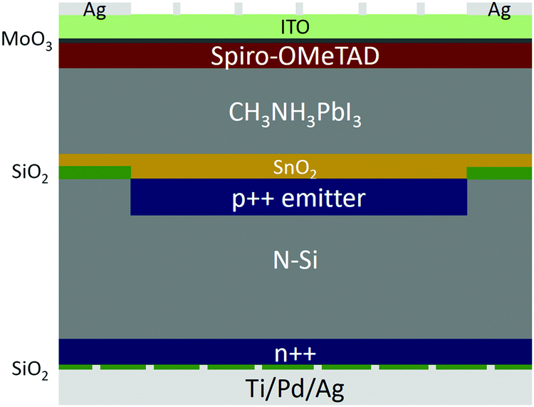 | ||
| Fig. 1 Schematic device design of interface-layer-free perovskite/silicon-homojunction solar cells (not to scale). | ||
With regards to the top perovskite cell structure, although theoretically a band gap near 1.7 eV has been recommended in the absence of any optical loss,29,30 parasitic absorption of short wavelengths exists in the hole transport materials (HTM) commonly used in state of the art solar cells4,7,9,16,31 such as poly[bis(4-phenyl)(2,5,6-trimethylphenyl)]amine (PTAA),4,9 and 2,2′,7,7′-tetrakis(N,N-di-p-methoxyphenylamine)-9,9-spirobifluorene (spiro-OMeTAD).4,31 Parasitic absorption of short wavelength light also exists in the ITO/MoO3 stack, which is also the most commonly used transparent conductive stack for the top of the semi-transparent perovskite in a tandem.17,32 The thin MoO3 protects the perovskite cell from sputter damage from the deposition of ITO, which is responsible for electrical conduction. Absorption in the ITO/MoO3/HTM stack hinders the effectiveness of the use of the high bandgap perovskite. In addition, the higher voltage output expected from higher bandgap perovskite materials is yet to emerge. In fact, a recent study by Hörantner et al.33 simulating the energy yield of a perovskite/Si tandem has recommended the use of a slightly lower bandgap (1.65 eV) material for the 2-terminal tandem. Energy yield calculations for 3 locations (Golden, Mohave and Seattle in the US) for stationary, 1-axis and 2-axis tracking systems all concluded that the use of a 1.6 eV material as the absorber for the top cell would only reduce the annual energy yield by 2–3% from the maximum achievable. Given the reasons above, MAPbI3 is chosen as the perovskite light harvesting material for the top cell in our tandem demonstration. In addition, in order to show the effectiveness of the interface-free layer design for large areas, the minimum area for tandem cell demonstration is 4 cm2 in this work. A schematic of the interface-layer-free perovskite/silicon-homojunction solar cells is shown in Fig. 1 and details of fabrication of the top and bottom cells are given in the Experimental section.
Initial optimization
To determine the optimum thickness of the SnO2 layer, an opaque cell structure of Au//spiro-OMeTAD/MAPbI3/SnO2/ITO glass is used. SnO2 at 9 nm, 15 nm and 28 nm has been trialled. The distributions of PCE, FF, JSC, VOC and RS are summarized in Fig. S1a–e (ESI†). At the optimized thickness of 15 nm, the PCE of the best performing cell is at 18.0% due to a better FF and high VOC (the J–V curve is shown in Fig. S1f, ESI†). The better reproducibility associated with 15 nm thick SnO2 (Fig. S1a, ESI†) could be due to better uniformity resulting in a narrower FF distribution compared to the 9 nm SnO2 case. When the SnO2 is too thick, (e.g., at 28 nm), VOC, JSC, FF and RS deteriorate due to poor conductivity.For the purpose of optimizing the MAPbI3 cell for current matching with the bottom silicon cell in the monolithic tandem, the thickness of MAPbI3 is allowed to range from 260 nm to 470 nm while the thickness of spiro-OMeTAD is fixed at ∼200 nm. The MAPbI3 layer in this work is fabricated using a two-step method (see the Experimental section for details) and the band gap is confirmed to be 1.58 eV (see Fig. S2 for optical measurement results and Fig. S3, ESI† for a typical X-ray diffraction (XRD) pattern). Fig. S4 (ESI†) shows the cross sectional scanning electron microscopy (SEM) images of the tandem devices with different thicknesses of MAPbI3 at 260, 380 and 470 nm. Fig. 2a shows the current density–voltage (J–V) curves of the corresponding devices while Fig. 2b shows the corresponding external quantum efficiencies (EQE) measured. It can be seen that when the thickness of MAPbI3 equals 260 nm, the perovskite cell is too thin and becomes current limiting (JSC = 12.5 mA cm−2). When the thickness of MAPbI3 equals 470 nm, the perovskite cell absorbs a large proportion of the light between 500 nm and 800 nm resulting in insufficient absorption in the Si cell for current matching, resulting in a JSC of 12.2 mA cm−2. When the thickness of MAPbI3 equals 380 nm, the output currents from the cells are well-matched (13.7 mA cm−2). The best 4 cm2 cell has a PCE of 16.3% with a VOC of 1583 mV, and a FF of 75%. This represents around a 20% improvement in PCE after the optimization of the MAPbI3 thickness. The effect of perovskite thickness on the current output can also be seen in the measured EQE in Fig. 2b, showing the same trend. An optical model is also established and performed using SunSolve™ ray tracing from PVLighthouse34 to simulate the effect of perovskite thickness on the bottom silicon cell as shown in Fig. S5 (ESI†). Although the JSC is overestimated in the model as the SunSolve™ ray tracing does not allow for carrier recombination input, similar trends are observed in the modelled EQEs with changes in MAPbI3 thickness. The similar peaks in the modelled EQEs also indicate that the model is able to account for the optical effects of the individual layers.
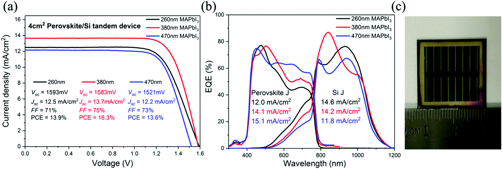 | ||
| Fig. 2 (a) J–V curves and (b) EQE of the tandem devices with different thicknesses of the MAPbI3 perovskite layer (260, 380 and 470 nm). (c) A photo of a fabricated 4 cm2 tandem device. | ||
Tandem interface investigation
To investigate the transport mechanism at the SnO2/p++ Si interface and the effect of p++ doping on the SnO2/p++ Si interface, Sentaurus technology computer-aided design (TCAD) modelling is carried out. Details regarding the TCAD simulation are given in the Experimental section while parameters are listed in Table 1. It is important to mention that, in order to obtain good wettability for the silicon surface, an ultra-violet ozone (UVO) treatment for the silicon substrate is performed before SnO2 deposition resulting in the formation of an unavoidable native SiO2 layer (∼1.5 nm measured by ellipsometry). The stoichiometry is confirmed by X-ray photoelectron spectroscopy (XPS) measurements (results shown in Fig. S6, ESI†). Therefore, this native SiO2 layer is also included in our model. Fig. 3a shows the results of the simulated dark J–V curves of the SnO2/p++ Si interface and as a function of p++ doping concentration. The J–V characteristics follow a diode behaviour. The inset of Fig. 3a shows the band diagram with the existence of a barrier due to the existence of the native oxide formed by the UVO treatment of the p++ silicon before the deposition of SnO2. Although the height of the barrier is substantial (2 eV), the oxide is thin enough to allow current transport via tunnelling. To verify this, the dark J–V of a test structure illustrated in the inset of Fig. 3b is measured. The test structure is fabricated by spin-coating a SnO2 (15 nm) layer on a UVO-treated heavily doped p++ silicon wafer (0.001–0.006 Ω cm) with a doping concentration of around 5 × 1019 cm−3. An ohmic contact is formed on the rear of the test structure via a sintered Ti/Pd/Ag stack. Silver (80 nm) was then deposited on the front followed by dark current density–voltage (J–V) measurement. As shown in Fig. 3b, the measured dark J–V curve verifies the transport mechanism due to the good agreement between the modelled and measured J–V curves.| Parameters | Electron | Hole | Unit | |
|---|---|---|---|---|
| SnO2 | Relative permittivity35 | 9.86 | ||
| Thickness | 0.015 | μm | ||
| Electron affinity36 | 4.2 | eV | ||
| Bandgap37 | 4.0 | eV | ||
| Electron concentration38 | 1 × 10²⁰ | cm−3 | ||
| Density of states | 1 × 10²¹ | 1 × 10²¹ | cm−3 | |
| Constant mobility39 | 1 × 10⁻⁴ | 2 | cm2 V−1 s−1 | |
| SRH lifetime40 | 1 × 10⁻¹² | 1 × 10⁻¹² | s | |
| SiO2 | Tunnelling mass41 | 0.4 | 0.4 | m 0 |
| Si | Thickness | 300 | μm | |
| SRH lifetime | 1 × 10⁻³ | 1 × 10⁻³ | s | |
| SiO2/Si | Interface recombination velocity | 1 × 10⁵ | 1 × 10⁵ | cm s−1 |
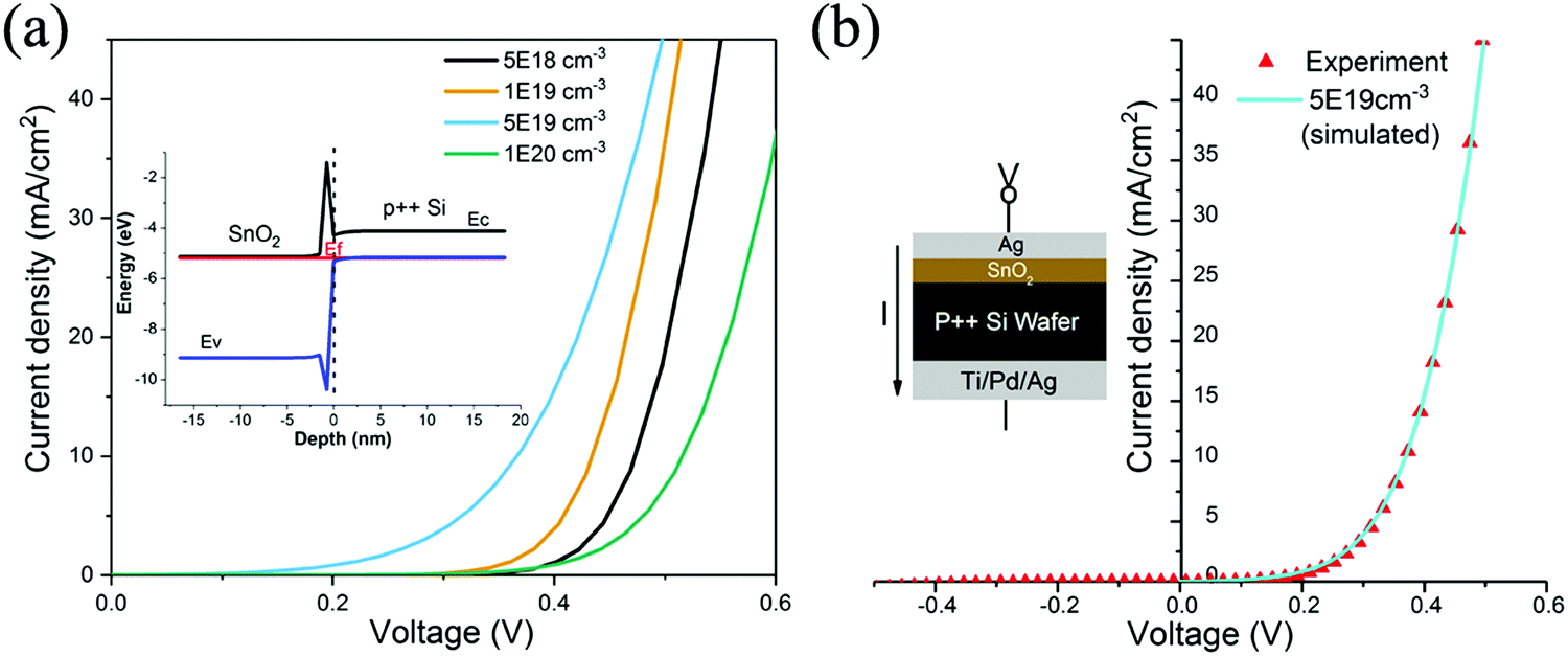 | ||
| Fig. 3 (a) Simulated dark J–V curves for the SnO2/p++ silicon interface when the p++ doping concentration is varied. Inset: Corresponding band diagram taking into account the effect of native SiO2. (b) Dark J–V characteristics of the Ag/SnO2/p++ Si/Ag test device (the inset shows the structure of the test device). | ||
In the previous section, p++ with a doping concentration of 1 × 1019 cm−3 was used for the front emitter of the Si cell. However, results of the modelling indicate that a doping concentration of 5 × 1019 cm−3 results in improved J–V characteristics due to enhanced interface recombination for current transport. SnO2 has a high electron density of 1 × 1020 cm−3 and a relatively low electron affinity of 4.2 eV. When it is brought together with p++ Si, their Fermi levels need to be aligned so that no current flows at thermal equilibrium conditions. The alignment of Fermi levels forces the bands of SnO2 to bend upwards while those of Si bend downwards. This can be seen in the modelled band diagrams in Fig. S7a–d (ESI†) showing the interface recombination variation with different p++ doping concentrations at the bias voltage of 0.4 V. When the p++ doping is below 5 × 1019 cm−3, the Si surface is inverted and holes are the minority carriers at the surface. As excess carriers are injected, the interface recombination is limited by holes. As the p++ doping increases, the interface recombination increases as well. However, if the p++ doping increases further above 5 × 1019 cm−3, the Si surface is no longer inverted and electrons are the minority carriers at the Si surface. A heavier p++ doping, e.g. 1 × 1020 cm−3, will further repel electrons from the Si surface, resulting in suppressed interface recombination and deteriorating J–V characteristics.
Effect of emitter doping on the Si bottom cell
In the previous section, tandem cells have been fabricated on Si cells with a p++ doping of 1 × 1019 cm−3. Based on the modelled results above, we therefore fabricate Si bottom cells (without SnO2) with the two different diffusion profiles: “heavy” (5 × 1019 cm−3) and “light” emitter (1 × 1019 cm−3) for comparison. These Si bottom cells are identical to the ones shown in Fig. 1 except a Ag grid as a front contact is deposited on top of the p++ emitter.Fig. 4a shows the J–V curves of Si bottom cells that have two different p++ emitter profiles: 125.1 ohm sq−1 and 15.1 ohm sq−1. The corresponding doping profiles of the same cells measured with electrochemical capacitance–voltage (ECV) are shown in Fig. 4b. These profiles show surface doping concentrations at 1 × 1019 cm−3 (“light” emitter) and 5 × 1019 cm−3 (“heavier” emitter), respectively. Cells with heavier doping have higher JSC, VOC, and FF due to reduced surface recombination caused by the better passivation provided by the heavier p++ doping. The FF is also improved due to the lower contact resistance provided by the heavier p++ contact. This results in better PCE as observed. Therefore it is anticipated that tandem cells using Si bottom cells with the heavier p++ emitter will benefit from (i) better performance from the Si bottom cell and (ii) better interface transport as predicted by the TCAD simulation.
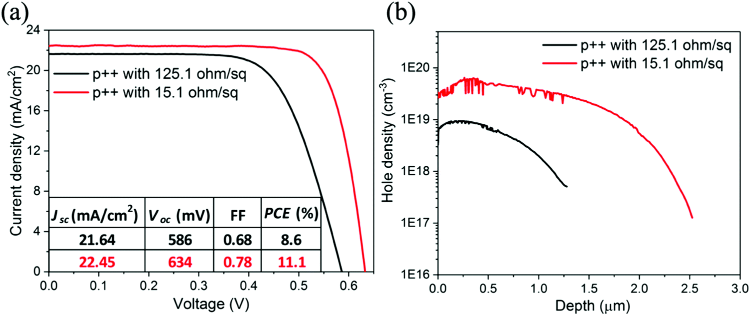 | ||
| Fig. 4 (a) Current density–voltage (J–V) curves of Si bottom cells that have different p++ emitter profiles (black for 125.1 ohm sq−1 and red for 15.1 ohm sq−1). (b) Doping profiles of the same cells measured with electrochemical capacitance–voltage measurements. | ||
Further optimization
It has been demonstrated that a textured anti-reflection (AR) foil featuring pyramidal features enhances the light harvesting ability of monolithic silicon/perovskite tandem devices17,22 due to the enhanced anti-reflection from the front and enhanced light trapping in the Si cell. Other work has shown that texturing that replicates the surface of a rose petal has even better anti-reflection properties.42,43 Therefore, we fabricated polydimethylsiloxane (PDMS) AR foil using a rose petal as a mould as shown in Fig. S8 (ESI†). The PDMS AR foil was then applied on the front of the tandem cell as illustrated in Fig. 5a. Fig. 5b shows the SEM cross sectional image of the cell with optimized thicknesses (SnO2 ∼ 15 nm, MAPbI3 ∼ 380 nm, spiro-OMeTAD ∼ 200 nm, MoO3 ∼ 18 nm, and ITO ∼ 100 nm).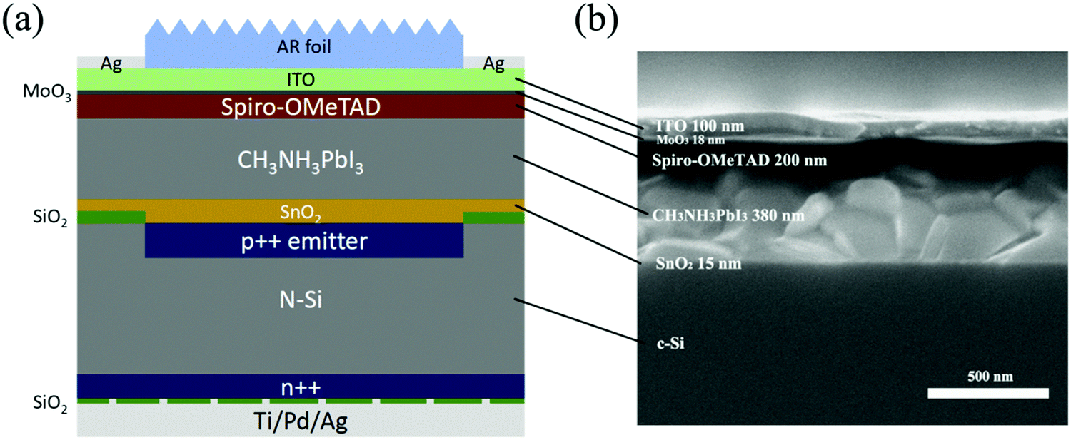 | ||
| Fig. 5 (a) Schematic device design of interface-layer-free perovskite/silicon-homojunction solar cells with PDMS AR foil coating (not to scale). (b) Cross sectional SEM image of the tandem device. | ||
Fig. 6a shows the J–V results of the tandem cell that uses the lightly doped p++ emitter for the Si bottom cell before and after the application of the AR foil. A dramatic increase in JSC by 1.9 mA cm−2 absolute can be seen in the measured J–V curve. As shown in Fig. 6b, the measured EQEs show improvements in current outputs from both the top and bottom cells due to enhanced front anti-reflection and enhanced light trapping in the bottom cell. The improvement in enhanced anti-reflection can be seen in the measured reflectance shown in Fig. 6c. Not only has the reflection been reduced, the interference effect that is manifested in large fluctuations in the reflection curve has been reduced as a result of applying the AR foil. In addition, light absorption between 400 nm and 800 nm is enhanced in the perovskite top cell and light absorption between 900 nm and 1000 nm is enhanced in the Si bottom cell. The short wavelength enhancement is due to better antireflection from the texturing and better refractive index matching provided by the PDMS. The long wavelength enhancement is due to the enhanced optical pathlength in the Si cell due to light trapping. The lack of improvement in absorption between 800 nm and 900 nm in the total EQE shown in Fig. 6d is due to negligible improvement in antireflection as seen in Fig. 6c. Nevertheless, the effectiveness of the AR foil that replicates the surface of a rose petal is demonstrated in the optical and electrical results of the perovskite/silicon tandem solar cell with improved performance.
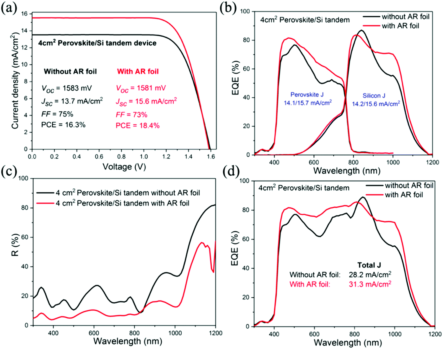 | ||
| Fig. 6 (a) J–V curves, (b) EQE, (c) reflectance and (d) “total” EQE of the best tandem device (MAPbI3 = 380 nm) that uses the lightly doped p++ emitter in the Si bottom cell before (black) and after (red) the application of the AR foil. The “total” EQE curve in (d) is the sum of the EQEs from the top perovskite and bottom silicon cells. | ||
Finally, the PDMS foil is applied on a 4 cm2 tandem cell with an optimised p++ Si/SnO2 interface by using a heavier p++ front diffusion (5 × 1019 cm−3 doping concentration) for the Si bottom cell. As shown in Fig. 7a, the PCE of the monolithic tandem cell increased from 18.4% to 21.0%. VOC under reverse scanning also improved by ∼100 mV to 1.68 V. JSC and FF also contributed to the PCE improvement with values of 16.1 mA cm−2 and 78%, respectively. For comparison, the J–V curve (under reverse scanning) of same cell without an AR foil is shown in Fig. S9 (ESI†). The steady state PCE is 20.5% (inset of Fig. 7a). It is important to note that the FF of 0.78 achieved in this work is the highest FF achieved of all demonstrated monolithic perovskite/silicon tandem devices larger than 1 cm2 to our knowledge (see Table S1, ESI,† which summarises results of demonstrated monolithic perovskite/silicon tandems to date). The EQE of the tandem device also improved due to reduced recombination as a result of better carrier transport between the cells from the improved p++/SnO2 interface.
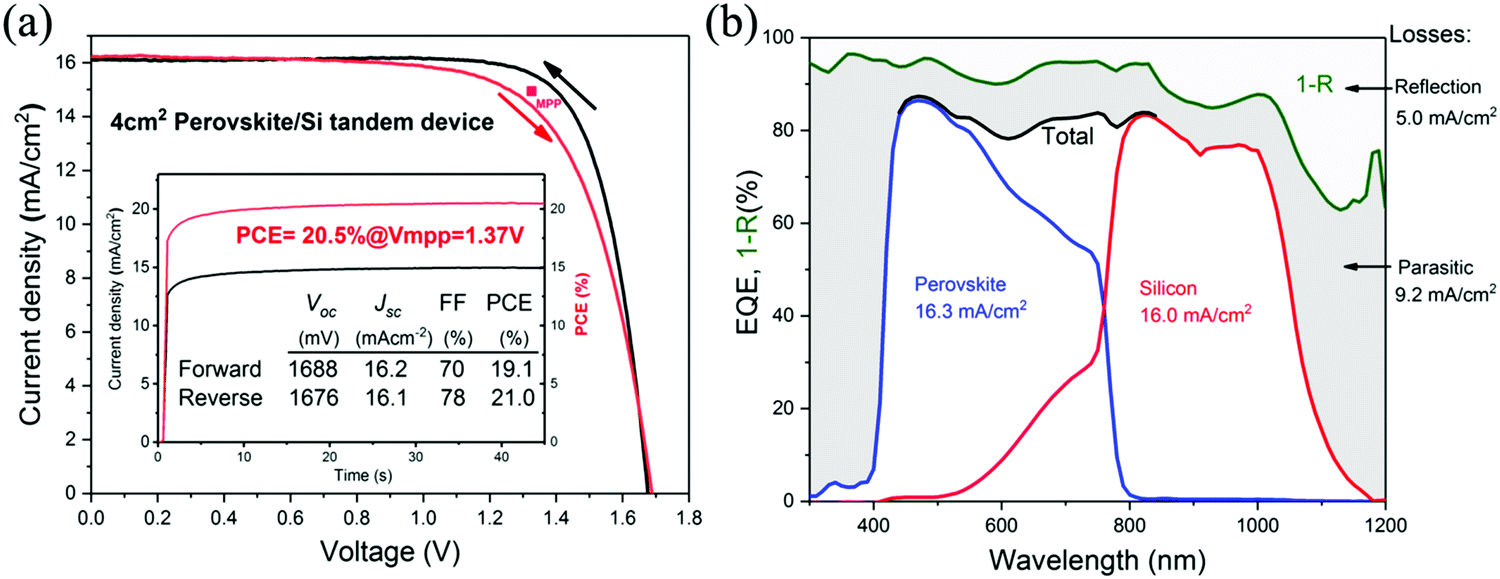 | ||
| Fig. 7 (a) J–V curve and in the inset: steady-state PCE of the champion tandem device on 4 cm2 using the heavier p++ front emitter for the Si bottom cell and with antireflection foil on the front of the tandem. (b) EQE for the corresponding device (black), for the perovskite top cell (blue), and for the silicon bottom cell (red). The total absorbance (1-reflectance) of the tandem device is shown by the green line. | ||
Demonstration of a large area tandem
Another advantage of using SnO2 as a recombination contact with the p++ Si emitter is the lack of lateral conduction in the SnO2 layer, thereby localising any shunting effects from imperfections in the perovskite cell. That is, the p++ Si/SnO2 is only responsible for vertical conduction between the top and bottom cells while the lateral conduction is managed by the p++ layer. This means up-scaling to large areas is not limited by the SnO2 layer, making it relatively straightforward to demonstrate large area devices. This is important as typical silicon solar cells can reach high efficiency on much larger areas. To date, only one study demonstrated a large area perovskite/silicon tandem cell over 10 cm2. Although a 4 cm2 cell with 20% efficiency has been demonstrated in this work, we further test the effectiveness of this design for large areas by fabricating a 16 cm2 tandem as shown in Fig. 8. As shown in Fig. 8a, a PCE of 17.6% under reverse-scanning is achieved with a VOC of 1.66 V, a JSC of 15.6 mA cm−2 and a FF of 68% on 16 cm2. The steady-state PCE is 17.1%. JSC (similarly EQE in Fig. 8b) and VOC of the large area device are slightly lower than (3–4% lower for JSC & 1–2% lower for VOC) those of the small area device. However, the drop in FF is more significant (by 12% relative or 10% absolute) as the area increases from the 4 cm2 to the 16 cm2 device. This is due to the un-optimized top metal grid design and thickness as RS in the current 16 cm2 device is estimated to be 10.7 Ω cm2, while for the 4 cm2 cell, RS is estimated to be 3.8 Ω cm2. To a smaller extent, non-uniformity of the perovskite and transport layers due to the limitation of the spin-coating process on a large area is also a cause for a reduced FF.20,44 This can be seen in the reduced RSH from 3042 Ω cm2 to 1113 Ω cm2 as the area of the cell increased from the 4 cm2 to the 16 cm2 cell, limiting the FF to 68%. Nevertheless, this FF is the highest for a perovskite/silicon tandem larger than 10 cm2 and the cell demonstrated here is also the largest for perovskite/silicon tandem reported to date.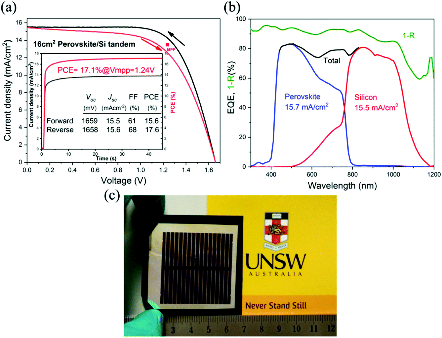 | ||
| Fig. 8 (a) J–V curve and the steady-state PCE in the inset for the champion tandem device on 16 cm2 using the heavier p++ front emitter for the Si bottom cell. (b) EQE for the corresponding tandem device (black), for the perovskite top cell (blue), and the silicon bottom cell (red). The total absorbance (1-reflectance) of the tandem device is shown by the green line. (c) A photo of a fabricated 16 cm2 tandem. | ||
Outlook
Although a steady state tandem PCE of 20% is achieved on 4 cm2 in this work, further improvements can be made. In particular the output short circuit current density at 16.1 mA cm−2 is lower than ideal considering an independently confirmed JSC at 18.1 mA cm−2 has been demonstrated.19 Parasitic absorption and recombination losses as represented by the grey area in Fig. 7b, that is, the area between the EQE of the tandem (black) and the 1-reflectance curve (green), are significant. Therefore an optical loss analysis was performed using SunSolve™ ray tracing from PVLighthouse.34 The simulated EQE and 1-R for the demonstrated cell are shown in Fig. S10 (ESI†). While close agreement can be achieved between the modelled and measured 1-R curves, the measured EQE is lower than the simulated EQE in the wavelength ranges: 580–790 nm and 1000–1200 nm. The grey area highlighted is due to recombination losses in the demonstrated top and bottom cells that cannot be accounted for by the SunSolve™ ray tracer. The differences between the modelled EQE and measured EQE in these two regions account for approximately 0.8 mA cm−2 and 1.7 mA cm−2, respectively. If we deduct these values from the JSC calculated from the simulated EQEs (17.0 mA cm−2 for the top cell and 17.5 mA cm−2 for the bottom cell), the results will match the JSC calculated from the measured EQEs (16.3 mA cm−2 and 16.0 mA cm−2 for the top and the bottom cells, respectively) for the purpose of identifying sources of optical losses. Fig. S11 (ESI†) shows the breakdown of optical losses from each layer. A major loss comes from the PDMS foil (3.4 mA cm−2) followed by losses in spiro-OMeTAD (1.9 mA cm−2) and in ITO (1.0 mA cm−2). As the use of the PDMS foil is still at an early stage, the thickness of the PDMS foil is not optimised. The 2 mm thick foil is highly absorptive in the whole wavelength range concerned. Fig. S12 (ESI†) shows the measured transmittance of a planar thin (0.3 mm) and thick (2.0 mm) PDMS layer. Note there is a constant reduction in broad-band absorption and a dramatic reduction in short and long wavelength absorption from the use of a thinner PDMS layer. The losses in the ITO/MoO3/spiro-OMeTAD stack are mainly in the short wavelength range (300 nm to 420 nm). This loss can be mitigated by replacing the MoO3/spiro-OMeTAD stack with a high refractive index inorganic hole transport layer such as NiOx,45 CuI46 or V2O5.47 Optical simulation of an improved cell structure AR foil/Ag grid/ITO/NiOx/MAPbI3/SnO2/Si/SiO2/Ag shows that a JSC close to 20 mA cm−2 can be achieved. Results are shown in Fig. S13 and Table S2 (ESI†) lists the thicknesses optimised for each layer to achieve current matching. The improvement in JSC is due to the elimination of parasitic absorption in the short wavelength range by replacing the MoO3/spiro-OMeTAD stack with NiOx, and a reduction in broad-band absorption by thinning of the AR foil. It is anticipated that rear texturing for the Si cell will also improve the optical performance for the tandem compared to the current design which uses planar Si bottom cells. The use of a thicker Si wafer (increasing the thickness from the current 300 μm to 450 μm in the future) will capitalize on the long lifetime of the wafer with good light trapping. To improve the overall VOC, a mixed cation mixed halide perovskite can be used to replace MAPbI3 used in this work, potentially increasing VOC from the current 1.1 V to 1.2 V as 1.24 V has been achieved with a 1.62 eV band gap perovskite solar cell.48With regards to further optimization of the SnO2/p++ Si interface, a TCAD simulation is performed for the case where the native SiO2 tunnel oxide is absent. The same assumptions (e.g., the same parameters from Table 1) are used. The simulated dark J–V curves are shown in Fig. S14 (ESI†). When a thin native SiO2 barrier is present in the present cells (Fig. 3), current transport via recombination is limited by the number of holes at the surface of SnO2 and the number of electrons at the surface of p++ Si. If the SiO2 barrier is removed (Fig. S14, ESI†), current transport will be enhanced due to enhanced recombination encouraging electron flow to p++ Si and hole transport to SnO2. By comparing the dark J–V curves between Fig. 3 and Fig. S14 (ESI†), we can see that the voltage drop at the interface (when the p++ doping concentration = 5 × 1019 cm−3) is effectively halved at the same current level. It may be possible to replace the UVO treatment with an oxygen plasma treatment of the Si surface to achieve a hydrophilic wettable surface for SnO2 deposition without the formation of a barrier oxide layer but only a monolayer of oxide.49 An added advantage of a plasma treatment is the resultant defective surface50 that aids the surface recombination for carrier transport between Si and SnO2.
To achieve a tandem efficiency of 30%, JSC > 20 mA cm−2, VOC > 1.8 V and FF > 0.8 (requiring RS < 2 Ω cm2) will be required. For a large area device, series resistance loss from the front Ag grid will need to be minimised warranting new designs.
3. Conclusions
In summary, we have developed a new monolithic perovskite/silicon-homo-junction tandem device structure without fabrication of an extra interface layer. This simple but effective structure uses a homo-junction silicon solar cell as the bottom cell, a planar CH3NH3PbI3 perovskite solar cell as the top cell and dual-function low temperature processed SnO2 which serves as an electron transport layer (ETL) and a recombination layer producing high performance and is easily scalable to large areas. Sentaurus technology computer-aided design (TCAD) modelling is used to understand the transport mechanism associated with the SnO2/p++ Si interface. The model is further used to predict tandem cell performance when the doping concentration of the p++ Si emitter is varied allowing further optimisation. Using an optimised p++ Si emitter and after the application of a front textured anti-reflection foil, a stabilized efficiency at 20.5% is achieved on 4 cm2 and a steady-state PCE of 17.1% is achieved on 16 cm2. To our knowledge, this is the highest reported for a monolithic perovskite/homo-junction-silicon tandem solar cell larger than 1 cm2. Details of optical modelling are also reported in this work allowing major optical losses to be identified. A monolithic tandem efficiency of 30% can be achieved if the VOC can be improved to 1.8 V and JSC can be improved to 20 mA cm−2. The latter requires the replacement of the MoO3/spiro-OMeTAD stack with a high refractive index inorganic hole transport layer, the use of thinner AR foil, and rear-texturing for the Si solar cells. Further optimisation of the ETL/Si interface such as the elimination of native SiO2 or the use of doped ETL for better band alignment and lower contact resistance is anticipated to improve the voltage output and fill factor (FF). A FF of 80% is also required for a 30% efficient tandem. This warrants a new front metal grid design, which plays a critical role in large area devices. This work paves the way to realize commercialisation of low cost, efficient, large-area perovskite/silicon homo-junction tandem solar cells.4. Experimental section
Device fabrication
A double-sided, polished, floating zone (FZ) 1–5 Ω cm n-type 〈100〉 Si wafer with a thickness of 300 μm was used to prepare a bottom cell. A phosphorus (POCl3) diffused n++ (130.0 ohm sq−1) high-low junction was formed on the rear side. A boron (BBr3) diffused p++ emitter (125.1 ohm sq−1 to 15.1 ohm sq−1) was formed on the front and was well defined to define the active area. The metal contact on the rear consists of Ti/Pd/Ag. The rest of the non-contacted rear was passivated by thermally grown and annealed SiO2.25 These polished silicon solar cells with an un-passivated p++ front were then directly used as a substrate for the fabrication of the top perovskite cell. To complete full tandem fabrication, the polished silicon solar cells were treated with a UVO cleaner for 6 min before SnO2 deposition. The SnO2 colloidal precursor (Alfa Aesar, tin(IV) oxide, 15% in H2O colloidal dispersion) was diluted with H2O to 3.75%. Then, the diluted SnO2 colloidal precursor was directly spin coated on the front of the silicon solar cells at 3000 rpm for 30 s, followed by baking on a hotplate at 150 °C for 30 min in air to form a compact SnO2 ETL. After cooling down, the SnO2 coated silicon substrates were directly transferred to a N2 filled glovebox for the fabrication of the MAPbI3 absorber using a two-step method. Different concentrations of PbI2 precursor were prepared by dissolving PbI2 powder (Alfa Aesar) of different weight (461 mg, 553 mg and 737 mg) in 1 mL dimethylformamide (DMF) (Sigma-Aldrich) with excess dimethyl sulfoxide (DMSO) (Sigma-Aldrich, 71 μL, 82 μL and 114 μL) which was then spin coated on the SnO2 coated silicon cell at 3000 rpm for 30 s. The MAI precursor (Greatcell Soalr) (dissolved in isopropyl alcohol (Sigma-Aldrich) at 40 mg mL−1; 50 mg mL−1; or 68 mg mL−1) was then spin-coated at 3000 rpm for 30 s. The samples were dried at 100 °C for 10 min producing dark brown dense MAPbI3 films with different thicknesses depending on the concentrations of precursors used.For the deposition of the hole transport material (HTM), the 2,2′,7,7′-tetrakis(N,N-di-p-methoxyphenylamine)-9,9-spirobifluorene (spiro-OMeTAD, Lumtec) precursor was firstly prepared by dissolving 72.3 mg spiro-OMeTAD, 28.8 μL 4-tert-butylpyridine (Sigma-Aldrich), and 17.5 μL lithium bis(trifluoromethylsulphonyl)imide (Sigma-Aldrich) solution (520 mg mL−1 in acetonitrile (Sigma-Aldrich)) and 8 μL FK209-cobalt(III)-TFSI (Lumtec) solution (300 mg FK209-cobalt(III)-TFSI in 1 ml of acetonitrile) in 1 mL chlorobenzene (Sigma-Aldrich). The spiro-OMeTAD precursor was then deposited onto MAPbI3 by spin-coating at 3500 rpm for 30 s.
For the front transparent electrode, 18 nm MoO3 (Sigma-Aldrich) was deposited on the spiro-OMeTAD by thermal evaporation at a rate of 0.7 Å s−1 under vacuum at 1 × 10⁻⁵ mTorr to protect the spiro-OMeTAD layer from sputtering damage during the deposition of indium tin oxide (ITO).22 The transparent contact was then fabricated by sputtering 100 nm ITO on the MoOx layer with 30 W RF power with Ar at 1.5 mTorr for 150 min using an AJA International sputtering system. A metal frame of silver was deposited by thermal evaporation to a thickness of 200 nm defining the active area of the cell. Finally, the front of the cell is covered by a textured polydimethylsiloxane (PDMS) foil for light trapping and antireflection (AR), see Fig. S8 (ESI†).
Measurements
The depth dependent doping profiles of the p++ emitter of half silicon cells were measured using an electrochemical capacitance–voltage (ECV, CVP21, WEP) analyzer, calibrated using ρsh to account for the surface roughness.51X-ray photoelectron spectroscopy (XPS) was carried out using an ESCALAB250Xi, Thermo Scientific, UK.
The current density–voltage (J–V) measurements of tandem devices were performed using a solar cell J–V testing system from Abet Technologies, Inc. (using a class AAA solar simulator) under an illumination power of 100 mW cm−2 with a metal aperture (4 cm2 and 16 cm2) and a scan rate of 30 mV s−1 in the direction from the open-circuit voltage (VOC) to the short-circuit current density (JSC) (1.8 V to −0.1 V). The J–V curves of the best tandem devices were also measured with a forward scan at a scan rate of 30 mV s−1 in the JSC to VOC direction (−0.1 V to 1.8 V). The light was calibrated using a certified reference cell. The bias voltage for the steady-state measurements was chosen as the average of the maximum power point (MPP) voltage of the J–V measurement.
The external quantum efficiency (EQE) measurement was carried out using the PV Measurement QXE7 Spectral Response system with monochromatic light from a xenon arc lamp. The EQE response was calibrated using two certified reference cells for the 300–1000 nm and 1000–1400 nm wavelength regions, respectively. A blue LED light (450 nm) and a near-infrared lamp were used to saturate the top and the bottom cell for the EQE measurement of the bottom silicon cell and the top perovskite cell, respectively.
The steady state photoluminescence (PL) measurements were made with an Andor iVac CCD detector (the detector temperature is −60 °C). The excitation wavelength of the CW laser was 409 nm and the signal was collected using a 0.2 second exposure time.
Top view and cross-sectional scanning electron microscopy (SEM) images were obtained using a field emission SEM (NanoSEM 230). The optical reflection and transmission spectra were measured using a Perkin Elmer Lambda1050 UV/vis/NIR spectrophotometer. All measurements were undertaken at room temperature in ambient conditions.
Optical simulations
The optical simulations of the perovskite/silicon tandem solar cell were performed using SunSolve™ ray tracing from PVLighthouse.34 Optically, silicon was treated to be bulk and non-coherent in the simulation. The simulation package does not allow for carrier recombination input. Therefore 100% internal quantum efficiency is assumed for both the top and bottom cells. The optical values (n, k) of SnO2, the perovskite, spiro-MeOTAD, MoO3 and ITO were all extracted from spectral ellipsometry measurements (JA Woollam Inc.) and fitted by WVASE® software. Other optical values (n, k) of PDMS, Ag and NiOx are obtained from PVLighthouse.34Electrical simulations
A commercial software package, Sentaurus technology computer-aided design (TCAD),52 was used to investigate the carrier transport mechanism between SnO2 and Si. The simulator solves Poisson, drift-diffusion and carrier conservation equations numerically until self-consistency is reached. The heterojunction was modelled with a similar approach to ref. 53. For Si, state-of-the-art models highlighted by Altermatt54 and the latest Auger model54 were applied in the simulation to accurately predict silicon characteristics. For SnO2, the key material parameters are determined from various papers35–40 as listed in Table 1. Several essential models are employed to compute carrier transport including Fermi statistics, and Shockley–Reed–Hall models.55,56 Due to the bandgap discontinuity at the hetero-interface, the thermionic emission model is applied to compute the current density and energy flux density across the interface. With the presence of silicon oxide between SnO2 and Si, the tunnelling mechanism is enabled with the same approach delineated in ref. 41.Author contributions
A. H.-B. and J. Z. conceived and designed all the experimental work. J. Z., C. L., and H. M. were involved in tandem device fabrications. J. Z., C. L., X. D. and A. S. performed measurements. J. Z., Y. J. and X. C. contributed to the optical simulations. F. M. contributed to the electrical stimulations. The manuscript was written by J. Z. and A. H.-B. All authors contributed to the discussion of the data, writing of the sections of the manuscript and revision of the manuscript. The overall project was supervised by M. G., S. H. and A. H.-B.Conflicts of interest
There are no conflicts to declare.Acknowledgements
The Australian Centre for Advanced Photovoltaics (ACAP) encompasses the Australian-based activities of the Australia-US Institute for Advanced Photovoltaics (AUSIAPV) and is supported by the Australian Government through the Australian Renewable Energy Agency (ARENA). This project is also supported by ARENA via the project 2014 RND075. The authors are grateful to Mr Benjamin Wilkinson (UNSW), Dr Weifei Fu (Zhejiang University) and Mr Yiliang Wu (Australian National University) for valuable suggestions. We thank the Electron Microscopy Unit and the BioMedical Imaging Facility at UNSW for the SEM and fluorescence imaging supports.References
- M. A. Green and A. Ho-Baillie, ACS Energy Lett., 2017, 2, 822–830 CrossRef.
- A. Kojima, K. Teshima, Y. Shirai and T. Miyasaka, J. Am. Chem. Soc., 2009, 131, 6050–6051 CrossRef PubMed.
- NREL, http://www.nrel.gov/ncpv/images/effciency_chart.jpg, accessed 6th March, 2018.
- W. S. Yang, B.-W. Park, E. H. Jung, N. J. Jeon, Y. C. Kim, D. U. Lee, S. S. Shin, J. Seo, E. K. Kim, J. H. Noh and S. I. Seok, Science, 2017, 356, 1376–1379 CrossRef PubMed.
- W. Shockley and H. J. Queisser, J. Appl. Phys., 1961, 32, 510 CrossRef.
- S. P. Bremner, C. Yi, I. Almansouri, A. Ho-Baillie and M. A. Green, Sol. Energy, 2016, 135, 750–757 CrossRef.
- J. Werner, L. Barraud, A. Walter, M. Bräuninger, F. Sahli, D. Sacchetto, N. Tétreault, B. Paviet-Salomon, S.-J. Moon, C. Allebé, M. Despeisse, S. Nicolay, S. De Wolf, B. Niesen and C. Ballif, ACS Energy Lett., 2016, 1, 474–480 CrossRef.
- B. Chen, Y. Bai, Z. Yu, T. Li, X. Zheng, Q. Dong, L. Shen, M. Boccard, A. Gruverman, Z. Holman and J. Huang, Adv. Energy Mater., 2016, 6, 1601128 CrossRef.
- T. Duong, Y. Wu, H. Shen, J. Peng, X. Fu, D. Jacobs, E. C. Wang, T. C. Kho, K. C. Fong, M. Stocks, E. Franklin, A. Blakers, N. Zin, K. McIntosh, W. Li, Y.-B. Cheng, T. P. White, K. Weber and K. Catchpole, Adv. Energy Mater., 2017, 7, 1700228 CrossRef.
- J. Peng, T. Duong, X. Zhou, H. Shen, Y. Wu, H. K. Mulmudi, Y. Wan, D. Zhong, J. Li, T. Tsuzuki, K. J. Weber, K. R. Catchpole and T. P. White, Adv. Energy Mater., 2017, 7, 1601768 CrossRef.
- H. Uzu, M. Ichikawa, M. Hino, K. Nakano, T. Meguro, J. L. Hernández, H.-S. Kim, N.-G. Park and K. Yamamoto, Appl. Phys. Lett., 2015, 106, 013506 CrossRef.
- C. D. Bailie, M. G. Christoforo, J. P. Mailoa, A. R. Bowring, E. L. Unger, W. H. Nguyen, J. Burschka, N. Pellet, J. Z. Lee, M. Grätzel, R. Noufi, T. Buonassisi, A. Salleo and M. D. McGehee, Energy Environ. Sci., 2015, 8, 956–963 RSC.
- T. Duong, N. Lal, D. Grant, D. Jacobs, P. Zheng, S. Rahman, H. Shen, M. Stocks, A. Blakers and K. Weber, IEEE J. Photovolt., 2016, 6, 679–687 Search PubMed.
- R. Sheng, A. W. Ho-Baillie, S. Huang, M. Keevers, X. Hao, L. Jiang, Y. B. Cheng and M. A. Green, J. Phys. Chem. Lett., 2015, 6, 3931–3934 CrossRef PubMed.
- J. P. Mailoa, C. D. Bailie, E. C. Johlin, E. T. Hoke, A. J. Akey, W. H. Nguyen, M. D. McGehee and T. Buonassisi, Appl. Phys. Lett., 2015, 106, 121105 CrossRef.
- J. Werner, A. Walter, E. Rucavado, S.-J. Moon, D. Sacchetto, M. Rienaecker, R. Peibst, R. Brendel, X. Niquille, S. De Wolf, P. Löper, M. Morales-Masis, S. Nicolay, B. Niesen and C. Ballif, Appl. Phys. Lett., 2016, 109, 233902 CrossRef.
- Y. Wu, D. Yan, J. Peng, T. Duong, Y. Wan, P. Phang, H. Shen, N. Wu, C. Barugkin, X. Fu, S. Surve, D. Walter, T. White, K. Catchpole and K. Weber, Energy Environ. Sci., 2017, 10, 2472–2479 RSC.
- J. Werner, C. H. Weng, A. Walter, L. Fesquet, J. P. Seif, S. De Wolf, B. Niesen and C. Ballif, J. Phys. Chem. Lett., 2016, 7, 161–166 CrossRef PubMed.
- K. A. Bush, A. F. Palmstrom, Z. J. Yu, M. Boccard, R. Cheacharoen, J. P. Mailoa, D. P. McMeekin, R. L. Z. Hoye, C. D. Bailie, T. Leijtens, I. M. Peters, M. C. Minichetti, N. Rolston, R. Prasanna, S. Sofia, D. Harwood, W. Ma, F. Moghadam, H. J. Snaith, T. Buonassisi, Z. C. Holman, S. F. Bent and M. D. McGehee, Nat. Energy, 2017, 2, 17009 CrossRef.
- F. Sahli, B. A. Kamino, J. Werner, M. Bräuninger, B. Paviet-Salomon, L. Barraud, R. Monnard, J. P. Seif, A. Tomasi, Q. Jeangros, A. Hessler-Wyser, S. De Wolf, M. Despeisse, S. Nicolay, B. Niesen and C. Ballif, Adv. Energy Mater., 2017, 8, 1701609 CrossRef.
- R. Fan, N. Zhou, L. Zhang, R. Yang, Y. Meng, L. Li, T. Guo, Y. Chen, Z. Xu, G. Zheng, Y. Huang, L. Li, L. Qin, X. Qiu, Q. Chen and H. Zhou, Sol. RRL, 2017, 1, 1700149 CrossRef.
- S. Albrecht, M. Saliba, J. P. Correa Baena, F. Lang, L. Kegelmann, M. Mews, L. Steier, A. Abate, J. Rappich, L. Korte, R. Schlatmann, M. K. Nazeeruddin, A. Hagfeldt, M. Grätzel and B. Rech, Energy Environ. Sci., 2016, 9, 81–88 RSC.
- C. O. Ramírez Quiroz, Y. Shen, M. Salvador, K. Forberich, N. Schrenker, G. D. Spyropulos, T. Huemueller, B. Wilkinson, T. Kirchartz, E. Spiecker, P. J. Verlinden, X. Zhang, M. Green, A. W. Y. Ho-Baillie and C. J. Brabec, J. Mater. Chem. A, 2018, 6, 3583–3592 RSC.
- M. A. Green, Nat. Energy, 2016, 1, 15015 CrossRef.
- J. Zhao, A. Wang and M. A. Green, Prog. Photovolt.: Res. Appl., 1999, 7, 471–474 CrossRef.
- J. Zhao, A. Wang and M. A. Green, IEEE Trans. Electron Devices, 1994, 41, 1592–1594 CrossRef.
- A. W. Blakers, A. Wang, A. M. Milne, J. Zhao and M. A. Green, Appl. Phys. Lett., 1989, 55, 1363–1365 CrossRef.
- International Technology Roadmap for Photovoltaic (ITRPV) – 2016 results including maturity report (8th Edition, September 2017), http://www.itrpv.net/.cm4all/iproc.php/ITRPV%20Eighth%20Edition%202017-%20Maturity%20Report%2020170906.pdf?cdp=a, accessed 4th March, 2018.
- Z. J. Yu, M. Leilaeioun and Z. Holman, Nat. Energy, 2016, 1, 16137 CrossRef.
- M. H. Futscher and B. Ehrler, ACS Energy Lett., 2017, 2, 2089–2095 CrossRef PubMed.
- X. Li, D. Bi, C. Yi, J.-D. Décoppet, J. Luo, S. M. Zakeeruddin, A. Hagfeldt and M. Grätzel, Science, 2016, 353, 58–62 CrossRef PubMed.
- Y. Jiang, I. Almansouri, S. Huang, T. Young, Y. Li, Y. Peng, Q. Hou, L. Spiccia, U. Bach, Y.-B. Cheng, M. A. Green and A. Ho-Baillie, J. Mater. Chem. C, 2016, 4, 5679–5689 RSC.
- M. T. Hörantner, T. Leijtens, M. E. Ziffer, G. E. Eperon, M. G. Christoforo, M. D. McGehee and H. J. Snaith, ACS Energy Lett., 2017, 2, 2506–2513 CrossRef.
- PVlighthouse, https://www.pvlighthouse.com.au/sunsolve, accessed 4th December, 2017.
- H. J. van Daal, J. Appl. Phys., 1968, 39, 4467–4469 CrossRef.
- A. M. Ganose and D. O. Scanlon, J. Mater. Chem. C, 2016, 4, 1467–1475 RSC.
- A. Klein, C. Körber, A. Wachau, F. Säuberlich, Y. Gassenbauer, S. P. Harvey, D. E. Proffit and T. O. Mason, Materials, 2010, 3, 4892–4914 CrossRef PubMed.
- K. Wijeratne, J. Akilavasan, M. Thelakkat and J. Bandara, Electrochim. Acta, 2012, 72, 192–198 CrossRef.
- X. Ren, D. Yang, Z. Yang, J. Feng, X. Zhu, J. Niu, Y. Liu, W. Zhao and S. F. Liu, ACS Appl. Mater. Interfaces, 2017, 9, 2421–2429 CrossRef PubMed.
- P. R. Guagliardo, E. R. Vance, Z. Zhang, J. Davis, J. F. Williams, S. N. Samarin and E. C. Dickey, J. Am. Ceram. Soc., 2012, 95, 1727–1731 CrossRef.
- H. Steinkemper, F. Feldmann, M. Bivour and M. Hermle, IEEE J. Photovolt., 2015, 5, 1348–1356 Search PubMed.
- R. Schmager, B. Fritz, R. Hünig, K. Ding, U. Lemmer, B. S. Richards, G. Gomard and U. W. Paetzold, ACS Photonics, 2017, 4, 2687–2692 CrossRef.
- K. Li, Y. Zhang, H. Zhen, H. Wang, S. Liu, F. Yan and Z. Zheng, J. Mater. Chem. A, 2017, 5, 969–974 RSC.
- J. Kim, J. S. Yun, Y. Cho, D. S. Lee, B. Wilkinson, A. M. Soufiani, X. Deng, J. Zheng, A. Shi, S. Lim, S. Chen, Z. Hameiri, M. Zhang, C. F. J. Lau, S. Huang, M. A. Green and A. W. Y. Ho-Baillie, ACS Energy Lett., 2017, 2, 1978–1984 CrossRef.
- J. Zheng, L. Hu, J. S. Yun, M. Zhang, C. F. J. Lau, J. Bing, X. Deng, Q. Ma, Y. Cho, W. F. Fu, C. Chen, M. A. Green, S. Huang and A. W. Y. Ho-Baillie, ACS Appl. Energy Mater., 2018, 1, 561–570 CrossRef.
- J. A. Christians, R. C. Fung and P. V. Kamat, J. Am. Chem. Soc., 2014, 136, 758–764 CrossRef PubMed.
- Y. H. Lou and Z. K. Wang, Nanoscale, 2017, 9, 13506–13514 RSC.
- M. Saliba, T. Matsui, K. Domanski, J.-Y. Seo, A. Ummadisingu, S. M. Zakeeruddin, J.-P. Correa-Baena, W. R. Tress, A. Abate and A. Hagfeldt, Science, 2016, 354, 206–209 CrossRef PubMed.
- S. B. Habib, E. Gonzalez and R. F. Hicks, J. Vac. Sci. Technol., A, 2010, 28, 476–485 CrossRef.
- S.-W. Choi, W.-B. Choi, Y.-H. Lee, B.-K. Ju, M.-Y. Sung and B.-H. Kim, J. Electrochem. Soc., 2002, 149, G8–G11 CrossRef.
- R. Bock, P. P. Altermatt and J. Schmidt, Proc. 23rd EUPVSEC, Valencia, 2008 Search PubMed.
- T. Sentaurus, Technology computer aided design (TCAD), Synopsys, Zürich, Switzerland, 2016 Search PubMed.
- J. Zhao, F. J. Ma, K. Ding, H. Zhang, J. Jie, A. Ho-Baillie and S. P. Bremner, Appl. Surf. Sci., 2018, 434, 102–111 CrossRef.
- P. P. Altermatt, J. Comput. Electron., 2011, 10, 314 CrossRef.
- W. Shockley and W. Read Jr, Phys. Rev., 1952, 87, 835 CrossRef.
- R. N. Hall, Phys. Rev., 1952, 87, 387 CrossRef.
Footnotes |
| † Electronic supplementary information (ESI) available. See DOI: 10.1039/c8ee00689j |
| ‡ These authors contributed equally to this work. |
| This journal is © The Royal Society of Chemistry 2018 |