
Tailoring the microstructure and charge transport in conjugated polymers by alkyl side-chain engineering†
Sadiara
Fall
a,
Laure
Biniek
b,
Yaroslav
Odarchenko
c,
Denis V.
Anokhin
de,
Grégoire
de Tournadre
f,
Patrick
Lévêque
a,
Nicolas
Leclerc
g,
Dimitri A.
Ivanov
*cd,
Olivier
Simonetti
f,
Louis
Giraudet
f and
Thomas
Heiser
*a
aLaboratoire ICube, DESSP, Université de Strasbourg, CNRS, 23, rue de Loess, 67037 Strasbourg, France. E-mail: thomas.heiser@unistra.fr
bICS, Université de Strasbourg, 23 rue de Loess, 67034 Strasbourg, France
cInstitut des Sciences des Matériaux de Mulhouse, CNRS UMR 7361, 15 rue Jean Starcky, B.P. 2488, 68057 Mulhouse Cedex, France. E-mail: dimitri.ivanov.2014@gmail.com
dlomonosov Moscow State University, Faculty of Fundamental Physical and Chemical Engineering, GSP-1, 1-51 Leninskie Gory, Moscow, 119991, Russia
eIPCP RAS, Semenov Prospect 1, Chernogolovka, 141432, Russia
fLaboratoire de Recherche en Nanosciences, Université Reims Champagne Ardenne, Moulin de la Housse, 51687 Reims, France
gICPEES, Université de Strasbourg, Ecole Européenne de Chimie, Polymères et Matériaux, 25 rue Becquerel, 67087 Strasbourg, France
First published on 24th November 2015
Abstract
Charge transport in conjugated polymers is critical to most optoelectronic devices and depends strongly on the polymer structure and conformation in the solid state. Understanding the correlations between charge carrier mobility, energy disorder and molecular assembly is therefore essential to improve device performances. Alkyl side-chains contribute to intermolecular interactions and are key to controlling the polymer microstructure and electronic properties. Investigating a set of polymers with common conjugated units but different side-chain functionalization provides new insights into the complex structure–transport relationship. Here, field-effect transistors and space-charge-limited current devices are used together with in situ grazing-incidence wide-angle X-ray scattering to study charge transport and morphology in a series of donor–acceptor copolymers. Probing hole mobility as a function of carrier density and orientation permits us to assess energy disorder and hopping rate anisotropy, while X-ray diffraction allows us to link transport properties to the polymer microstructure. We show that branched side-chains enhance structural and energy disorder and lead to isotropic transport, whereas linear chains induce either a common lamellar structure or a more exceptional pseudo-hexagonal columnar phase with a helicoidal polymer conformation. The latter enhances out-of-plane mobility but increases energy disorder possibly due to larger interring torsion angles.
1. Introduction
Charge transport in semiconducting polymers is a key factor for the operation of most organic optoelectronic devices and has attracted a lot of attention from the scientific community over the last few decades. Although significant progress has been achieved in the design of polymers exhibiting relatively high charge carrier mobilities, the multifaceted relationship between the polymer molecular structure and the charge transport properties remains a challenging field of investigation.1–4 The complex link between molecular structure and transport originates from the fact that subtle variations in intra-molecular charge delocalization and inter-molecular coupling strength can have a strong impact on charge carrier hopping rates. Both intermolecular and intramolecular hopping depend in a non-trivial way on molecular planarity, chain length, chain folding, molecular packing, as well as on the nature and grafting position of alkyl side-chains. For instance, as shown by Vukmirović using atomistic multiscale modelling, the electronic density of states (DOS), which underlies charge transport, is expected to broaden with conjugated backbone shape irregularities and interring torsions introduced by alkyl side-chains.5 On the other hand, however, side-chains are also predicted to weaken fluctuations in the electrostatic coupling strength, thereby reducing energy disorder. Sirringhaus et al. recently confirmed the strong impact of side-chains on energy disorder for a range of state-of-the-art copolymers, and provided guidelines for the design of low disorder conjugated polymers.6 However, the structure–transport relationships are far from being fully understood.Since a predictive model for charge carrier mobilities in new conjugated polymers is not available, methodical experimental investigations of both electrical and morphological properties remain crucially important.3 Charge transport can be strongly anisotropic and dependent on charge carrier densities as well as on electric field strength. A profound understanding can therefore only be reached by probing charge transport along various orientations and in distinct electronic environments. The combined use of organic field-effect transistors (OFET) and space-charge-limited-current (SCLC) single carrier devices is a convenient way to approach this goal.7,8 Not only do both devices explore in-plane and out-of-plane (i.e. parallel or perpendicular to the device substrate) transport respectively, but their operation allows us furthermore to cover a large span of charge carrier densities and electric field intensities. This methodology has been used successfully before to investigate charge transport in poly(p-phenylene vinylene) and polythiophene derivatives.9 An eventual limitation of this approach lies in the possibility that the polymer microstructure may differ in both devices due to different substrates. This risk can however be minimized by combining charge transport measurements with in situ microstructure characterization.
In this work, we present an in-depth study of charge transport and thin-film microstructure of a series of conjugated low band-gap polymers which have been developed previously and used as electron-donors in bulk heterojunction solar cells.10,11 The polymers are composed of alternating electron-deficient benzo[2,1,3]thiadiazole (Bz) and electron-rich thiophene (Th) and thieno[2,3-b]thiophene (TT) units and differ essentially in the nature of their solubilizing side chains and in the number of thiophene units. The latter parameter controls the side-chain density along the polymer backbone since only thiophene units carry side-chains. While our previous investigations showed that these structural changes had a considerable impact on the material photovoltaic properties,10,11 we will focus herein on their influence on charge transport and thin film microstructure. Following the approach outlined above, we used OFET and SCLC devices to study the hole mobility, together with in situ GIWAXS experiments to characterize the thin film morphology. We show that minor modifications of the molecular structure can profoundly alter the microstructure and strongly impact transport anisotropy and energy disorder. In particular, branched side chains tend to enhance both structural and energy disorder, leading to a rather low isotropic hole mobility, while linear chains give rise to more ordered structures and strongly anisotropic transport. We further show that upon decreasing the side-chain grafting density along the polymer backbone the polymer assembly switches from a lamellar structure to an unusual helicoidal conformation, inducing an order of-magnitude change in the in-plane and out-of-plane hole mobilities. Interestingly, the out-of plane mobility, which is crucial to the operation of vertical devices such as organic solar cells, is enhanced by the helicoidal conformation.
2. Results
2.1 Materials
The molecular structures and relevant properties of the investigated polymers are summarized in Fig. 1. The synthesis procedures, as well as detailed molecular characterizations, have been published before.10 Shortly, the number of Th units per monomer was either 2 (for Ta, Tb) or 4 (for Pa, Pb). Linear dodecyl side chains were grafted on the Th units for Ta and Pa, while branched ethyl–hexyl chains were used for Tb and Pb. The molecular weights and ionization potentials, Ip, are within the same range for all four polymers, while the polydispersity index is slightly lower for Pa and Pb. | ||
| Fig. 1 Molecular structure and relevant properties of the investigated polymers. | ||
2.2 Charge transport
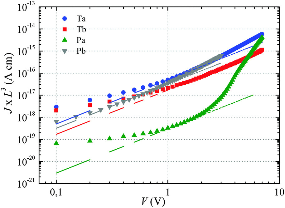 | ||
| Fig. 2 Space-charge-limited current on as-cast polymers. For Pa the curve has been obtained by averaging the current–voltage data of four devices processed under identical conditions. The dashed lines correspond to a fit in the voltage range where J follows a square-law dependence (constant mobility) on the voltage. | ||
If the current is space-charge-limited, the experimental curves should follow the conventional Mott–Gurney law,12
 | (1) |
The dashed lines in Fig. 2 have been obtained by fitting eqn (1) to the experimental curves in a voltage range where J follows a square-law dependence (constant mobility). This voltage range is limited at low values by Ohmic currents induced by either dark conductivity (unintentional doping) or carrier diffusion at the metal/semiconductor interface,13–15 while at high voltages, field-dependent16 and/or charge-carrier-density dependent charge transport may lead to a more pronounced current increase.9,17 For Ta, Tb and Pb the current follows the expected V2 law over a reasonable voltage range and can therefore be used to estimate the low-field out-of-plane mobility. This is not the case for Pa for which the presumable injection barrier allows only an estimate for the lower limit of mobility. The μ⊥ values are summarized in Table 1 and are of the same order of magnitude for Ta, Tb and Pb, while the estimate for the Pa mobility is two orders of magnitude lower. These results will be further discussed below.
| Polymer | Ta | Tb | Pa | Pb |
|---|---|---|---|---|
| μ ⊥ (cm2 V−1 s−1) | (1.3 ± 0.5) × 10−4 | (4.7 ± 1.0) × 10−5 | >10−6 | (8.5 ± 2.0) × 10−5 |
| μ ∥ (cm2 V−1 s−1) | (3.1 ± 0.3) × 10−5 | (5.5 ± 0.2) × 10−4 | (1.3 ± 0.3) × 10−3 | (5.5 ± 0.5) × 10−4 |
| E 0 (meV) | 32 ± 2 | 35 ± 1.5 | 28 ± 1 | 34 ± 1 |
 | (2) |
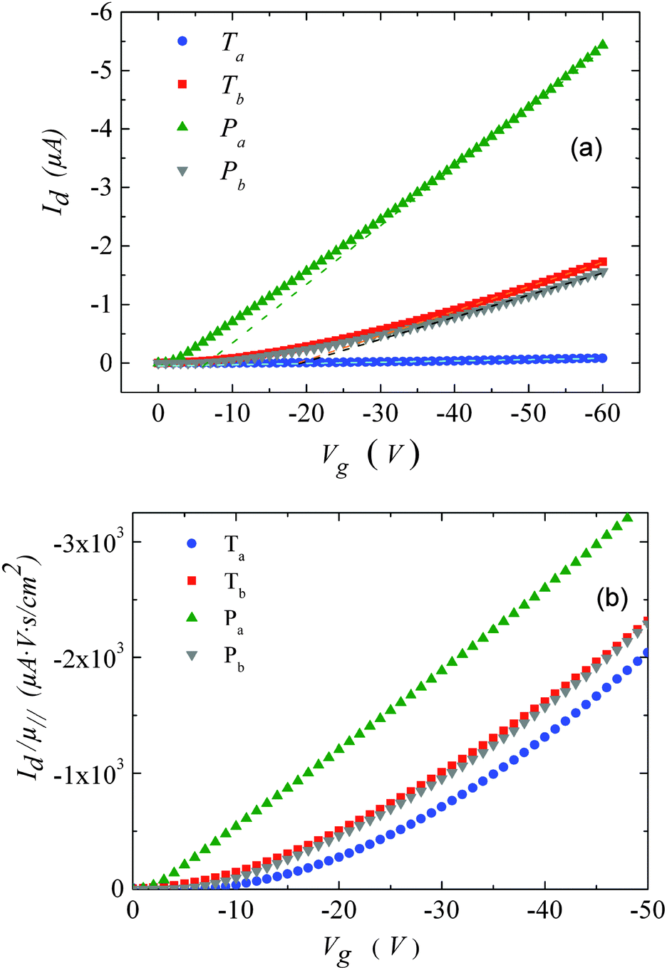 | ||
| Fig. 3 (a) Transfer characteristics measured at room temperature. (b) Drain current, normalized by the mobility values given in Table 1versus gate-voltage. The drain voltage was set to −10 V. | ||
For Tb and Pb, the μ∥ values are comparable (∼5 × 10⁻⁴ cm2 V−1 s−1) and exceed μ⊥ by roughly one order of magnitude. On the other hand a significantly higher μ∥ value (∼10−3 cm2 V−1 s−1) is found for Pa, about three orders of magnitude above the lower estimate of μ⊥. Surprisingly, the in-plane mobility of Ta (∼3 × 10⁻⁵ cm2 V−1 s−1) is about a factor of four lower than the corresponding out-of-plane mobility.
The strong contrast between the OFET and SCLC results can be partly explained by taking into account the influence of the charge carrier density (p) set by the gate voltage.19 Normalizing the drain current by the mobility given in Table 1 (Fig. 3b) highlights distinctive gate-voltage dependences. For Pa the drain current decreases almost linearly down to the threshold voltage, while for Ta, Tb and Pb, a significant positive curvature occurs at low Vg. As no contact resistance effects are seen neither in the OFET output characteristics (see ESI†) nor in the transfer characteristics at high gate voltages, it is likely that the non-linear transfer characteristics at low Vg are due to a charge carrier density dependent mobility. As μ∥ is proportional to the slope of Id (Vg), the mobility is seen to increase with the gate voltage for Ta, Tb, and Pb, while it remains almost constant for Pa. To go a step further in the comparison between SCLC and OFET results, we need to quantify p in both experiments. In SCLC devices, the charge carrier density is non-uniform over the semiconductor layer thickness and depends on the applied voltage and film thickness. An average value of p can nevertheless be obtained from the standard drift model of space-charge-limited transport,12,17 given by
 | (3) |
 | (4) |
Using both, the E0 estimates and eqn (3), we plotted the SCLC and OFET mobility values as a function of charge carrier density on the same graph (Fig. 4). The solid lines represent field-effect mobilities extrapolated to low charge carrier densities. The dashed lines represent the upper and lower limits for μ∥ taking into account the error margin on E0. Several conclusions can be drawn from Fig. 4. For the branched side-chain polymers Tb and Pb, the SCLC mobilities are significantly higher than the extrapolated field-effect values. This suggests the existence of a transition from a carrier density dependent to a constant mobility at a critical carrier density pc (indicated by an arrow in Fig. 4). According to the Gaussian disorder model (GDM), such a transition is expected to occur at a hole density given by24
 | (5) |
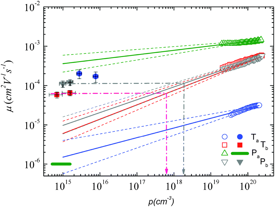 | ||
Fig. 4 Mobility as a function of the charge carrier density as measured in OFET (open symbols) and SCLC devices (full symbols) at room temperature. For SCLC measurements, eqn (3) was used to estimate p for an applied voltage of 1 V and two different film thicknesses. The green horizontal line indicates the lower limit of the SCLC mobility for Pa. The solid and dashed lines represent extrapolations of the field-effect mobility measured at a carrier concentration ph, corresponding to −60 V gate voltage (Table 1), down to a low carrier concentration pl, following 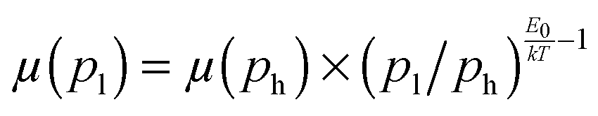 .21 For E0, the average values given in Table 1 (solid lines) as well as the upper and lower limits (dashed lines) have been used. The dash-dotted lines indicate the carrier concentration below which the hole mobilities in either Pb (grey line) or Tb (red line) are expected to remain constant. .21 For E0, the average values given in Table 1 (solid lines) as well as the upper and lower limits (dashed lines) have been used. The dash-dotted lines indicate the carrier concentration below which the hole mobilities in either Pb (grey line) or Tb (red line) are expected to remain constant. | ||
The situation is significantly different for Pa and Ta. In the case of Pa, the field-effect mobility extrapolated to low carrier densities is almost three orders of magnitude higher than the lower estimate of the SCLC mobility. The deviation from the Mott-Gurney law hampers however a quantitative comparison between both mobilities. Two possible scenarios may nevertheless be outlined: (i) the discrepancy between SCLC and OFET data is only due to the injection barrier in SCLC devices. Since the carrier density dependence appears to be weak (Fig. 4), the actual μ⊥ value should then be close to μ∥. (ii) The out-of-plane mobility is significantly lower than the in-plane mobility (anisotropic charge transport) and contributes to the observed high μ∥/μ⊥ ratio. The microstructural investigations shown below will help us to elucidate this question.
The most surprising result is obtained on polymer Ta. As shown in Fig. 4, the field-effect mobility exhibits a relatively pronounced charge carrier density dependence (high E0), which hints towards a disordered material with isotropic transport, similar to Tb and Pb. This conclusion is however in conflict with the measured out-of-plane mobility, which is almost one order of magnitude higher than μ∥. The latter result implies rather a high transport anisotropy, with a polymer microstructure that favors out-of-plane transport. In other words, the material appears to be characterized by a significant energy disorder but with a simultaneously high structural order (necessary to yield the observed transport anisotropy). Again, the microstructure analyses described below will help us to clarify this issue.
2.3 Polymer microstructure
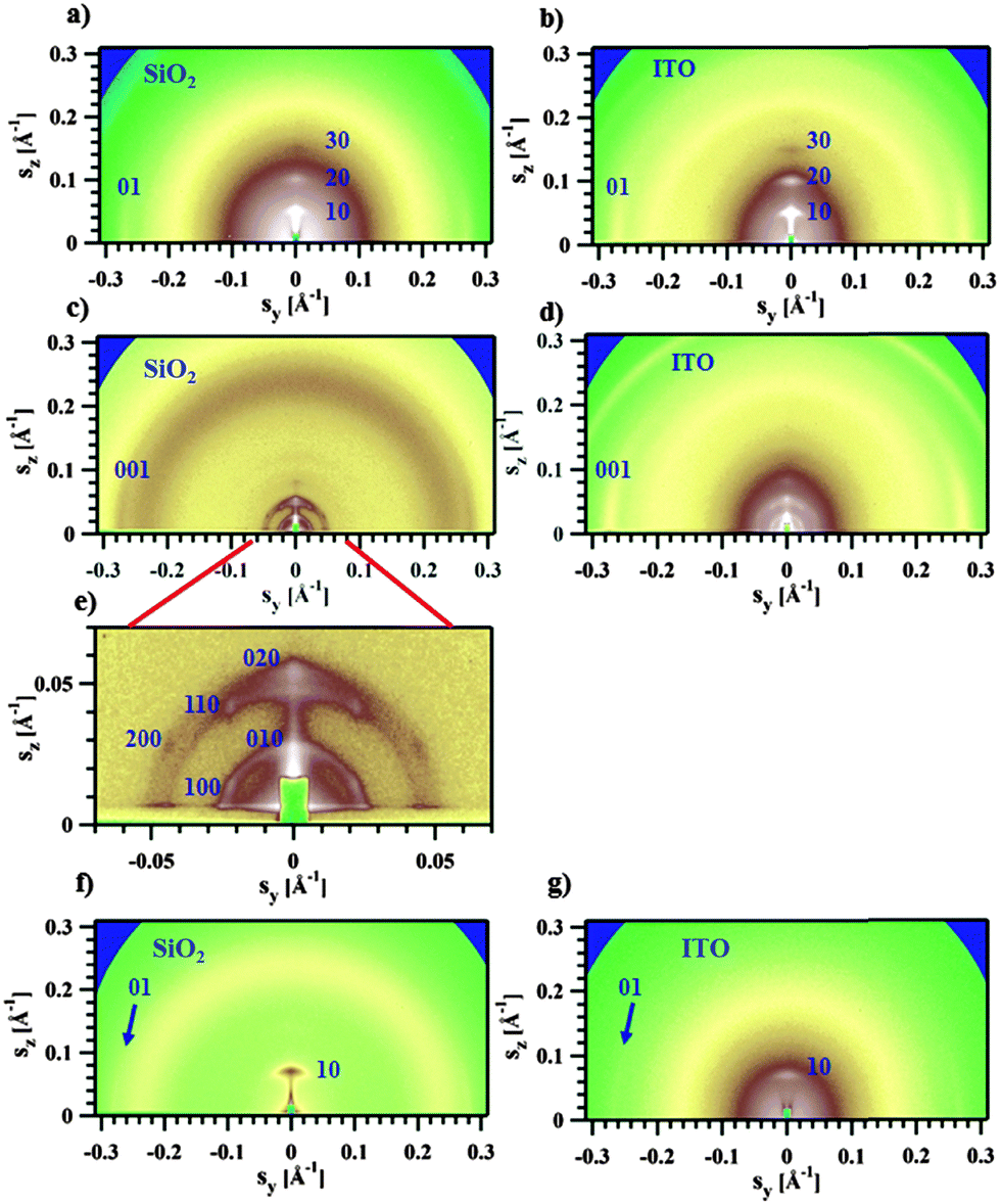 | ||
| Fig. 5 GIWAXS patterns for OFET (left) or SCLC (right) devices for Pa [(a) and (b)], Ta [(c) and (d)] and Tb [(f) and (g)]. (e) is an enlarged small-angle region of image in (c). The incidence angle is 0.2°. | ||
The GIWAXS experiments performed on films of Pa in the transistor geometry (Fig. 5a) show that the X-ray peaks are located exclusively on the meridian and the equator. The reflections were indexed to a 2D unit cell, as shown in Fig. 5a. A set of meridional h0 reflections corresponds to a pronounced layer-like structure with an in-plane orientation of the polymer backbones. In addition, the pattern reveals a characteristic π–π stacking peak at a distance of 3.72 Å, which is located at the equator (denoted as 01 peak in Fig. 5a). Consequently, the chains are parallel to the film surface with an edge-on π–π stacking of the aromatic cores (as schematically depicted in Fig. 6a). A similar morphology was previously reported for P3HT.26,27 The layer-like packing of the polymer chains is consistent with the high in-plane charge mobility measured for Pa. Noteworthily, the GIWAXS pattern measured on a SCLC device looks similar (Fig. 5b), indicating that identical morphologies are observed for this polymer on two different substrates.
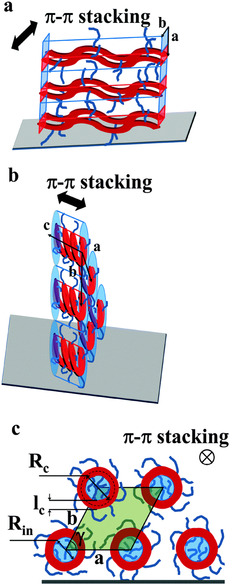 | ||
| Fig. 6 Models schematically depicting the layer-like structure of thin films of Pa (a) and Ta (b). The polymer backbone is represented in red while the film surface is the gray parallelogram. (c) The view along the helical axis represents notations used in eqn (7) and (8). The inner part of the helices is colored in blue, the area of the pseudo-hexagonal unit cell external to the helices is colored in green (c). | ||
The active layer of Ta reveals well-oriented GIWAXS patterns (Fig. 5c–e), which are significantly different from the patterns discussed above. The appearance of the pattern is typical of columnar structures.28 The analysis of the positions and intensities of the peaks in the small-angle region (Fig. 5e) makes it possible to assign the pattern to a monoclinic (pseudo-hexagonal) 2D columnar phase with the following parameters: a = 53.0 Å, b = 51.6 Å, γ = 47.6°. Moreover, the equatorial peak at 3.57 Å indicates the development of an intra-columnar ordering. The calculated distance is close to the π–π stacking discussed above (see Fig. 5a). Therefore, it is likely that Ta does not form regular layer-like structures as Pa, but forms instead a columnar structure with the in-plane columnar axis and the direction of π–π interactions parallel to the columnar axis. We speculate that for Ta the columns are formed from helices with the plane of the Th, TT and Bz rings normal to the helical axis. In this case, a dense packing of chemical units that constitute the neighboring helical pitches of the chain in the axial direction results in the formation of π–π interactions (Fig. 6b). Such intra-helical in-plane oriented π–π stacking can account for reasonable values of charge carrier mobility in the OFET geometry. It should be mentioned that experimental observations of a helical conformation for conjugated polymers are very scarce.29 However, theoretical calculations of the conformational energy have been performed for several non-substituted semiconducting homopolymers (e.g., polythiophene, polyfuran, and polypyrrol) showing that helical conformations of the conjugated backbone may be stable.29 In this respect, our results probably constitute one of the rare experimental evidences of a helical backbone conformation for this class of polymers. It should be mentioned that most of the semicrystalline polymers in the crystalline state adopt a helical conformation of the backbone, and the often-encountered planar conformation is just a particular case of a helix although it is not called so. However, the exceptional feature of the helical conformation of the Ta backbone inferred from the X-ray diffraction data is its extremely large diameter as compared to the monomer size.
The observed qualitative difference between the conformation of Ta and that of the other polymers can be accounted for by the relatively low volume of grafted alkyl side groups per unit length of the polymer backbone. It is probable that the lower grafting density for Ta in the fully extended conformation is not sufficient to fill the inter-chain space when forming a lamellar arrangement. To verify this argument, we have estimated the thickness of the layers formed by the conjugated backbones and alkyl groups in a hypothetical layer-like morphology. The thicknesses of the layer populated by the side chains (Ls) and the main backbone (Lc) are proportional to the ratio of the corresponding volumes (Vs and Vc, respectively):
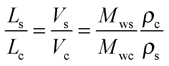 | (6) |
Another argument for the helical model is that the shortest distance between grafting points along the Ta backbone is ca. 9.1 Å. For a layer-like structure, assuming full interdigitation of the side chains, the shortest inter-chain distance between alkyl groups along the backbone axis will be equal to 4.55 Å. This value significantly exceeds the distance between the alkyl chains both in a pure n-alkane phase (for example, for n-octane the distance is 4.0 Å) and in the regions formed by the side chains of a P3HT lattice (3.9 Å). Consequently, the relatively long distance between grafting points prevents the formation of a layer-like structure in Ta. In contrast, the shortest distance between grafting points for Pa is ca. 5 Å, which is sufficient to form a dense alkyl layer. In the case of ethylhexyl substituted Tb and Pb the possibility of forming layer-like structures can be explained by a much lower density of the branched alkyl phase resulting in the formation of thicker side-chain layers.
The helical conformation in the Ta phase can compensate for the low density of the periphery. In addition, fine-tuning of the alkyl density can be achieved by varying the number of side chains inside (Nin) and outside (Nout) of the helix (shown as a red circle in Fig. 6c). A simple calculation given below allows the estimation of Nin and Nout for the helical conformation of Ta. The area of the helical chain cross-section Sc (coloured in red in Fig. 6c) and the area of the inner part of the helix Sin (coloured in blue) can be calculated from the number of monomers n per turn of the helix and the backbone length of a monomer L:
| Sc = nLlc | (7) |
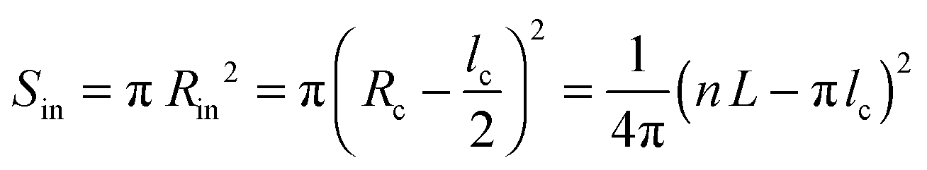 | (8) |
Sout = ab sin![[thin space (1/6-em)]](https://www.rsc.org/images/entities/char_2009.gif) γ − Sc − Sin γ − Sc − Sin | (9) |
Taking into account that the value of n found from the macroscopic density is equal to six, and L is approximately 17 Å, the values of Sc, Sin and Sout, calculated from eqn (7)–(9) are 514, 607 and 898 Å2, respectively. We consider that the packing density of the alkyl chains located inside and outside of the backbone is equal. In this case, the number of chains is proportional to the occupied volumes or surfaces. This allows us to find that Nin = 5 and Nout = 7. One can imagine that the alkyl density inside the helix can be lower because of the difficulty to efficiently pack in a narrow channel. If this is indeed the case, the difference between Nin and Nout will be even higher. The obtained value of Rc (16.3 Å) is in fair agreement with the radius calculated for polythiophenes using density functional theory30 (7.7 Å). It should be noted that the bigger radius of the helix in our case can be explained by the presence of bulky benzothiadiazole and thienothiophene groups in the backbone.
As far as charge transport is concerned, it is noteworthy that although the direction of the π–π stacking is along the columnar axes, the helical fragments of the chains can be relatively short. Non-regular loops of the helical backbones and ends of the chains, playing role of structural defects, can effectively overlap with the neighboring chains to provide good inter-chain charge transport. Also, because of a non-extended conformation of the alkyl groups, the distance between the main chains in the vertical direction of the columnar phase of Ta is shorter than that in the layer-like structure of Pa. This can be the reason for a relatively high inter-chain mobility for Ta in the direction perpendicular to the substrate.
3. General discussion and conclusion
The GIWAXS data support and clarify the conclusions of the charge transport study. For the branched side-chain polymers (Tb, Pb) the measured highly disordered thin film morphology is in line with the high-energy disorder observed by the mobility measurements (Fig. 4). On the other hand, for Ta and Pa, the GIWAXS structures reveal that charge transport is likely to be highly anisotropic. For Pa the pronounced lamellar morphology with in-plane π–π stacking interactions should favor in-plane transport and supports the inference that the orders of magnitude difference in OFET and SCLC mobilities is mostly due to anisotropic charge transport. The observed low energy disorder is then an expected outcome of the highly ordered microstructure. In addition, the more or less reproducible deviation from the Mott-Gurney law observed in Pa-based SCLC devices might be a consequence of the presence of a dense layer of alkyl chains at the PEDOT:PSS/Pa interface that hinders charge injection.The more intriguing charge transport observed in Ta thin films can also be clarified. The GIWAXS experiments show that Ta forms a rather unusual helical conformation of the conjugated backbone. Supposedly, the driving force for the helix formation in this structure with a relatively long distance between the chain grafting sites is the mismatch between the number of the side chains located inside and outside the helical scaffold. The regular turns of the helical backbone can account for the intra-chain π–π stacking in the direction parallel to the substrate, as revealed by a corresponding diffraction peak. Such structural organization comprising regular arrays of helices can account for a relatively high in-plane charge transport. In contrast, the shorter distance between neighboring helical polymer backbones in comparison to a perfectly layered structure, and the presence of conformational defects in Ta can explain why the value of μ⊥ is higher than μ∥. Interestingly, the higher interring torsion angles in such a helical conformation are expected to broaden the hopping site energy distribution.5 The helicoidal microstructure should therefore enhance energy disorder (through a strong intra-molecular contribution) while leading to a relatively ordered molecular assembly. This behavior clarifies why the charge transport measurements lead simultaneously to a strong transport anisotropy (μ⊥> μ∥) and a high-energy disorder typical of amorphous (isotropic) polymers.
In summary, by combining in-plane as well as out-of-plane charge transport measurements and grazing incidence X-ray diffraction investigations on the same devices, we were able to show how minor changes along the polymer backbone of a conjugated low band-gap copolymer family can significantly impact the molecular assembly and lead to different charge transport properties. Branched side chains are found to increase structural disorder and lead to a broad DOS distribution and isotropic transport, while linear chains give rise to more ordered structures and strongly anisotropic transport. We further found strong experimental evidence that rather a rigid conjugated polymer can adopt a helicoidal structure, induced by a density mismatch. Furthermore, the correspondingly lower backbone planarity and larger interring torsion angles are responsible for a broader energy distribution of hopping sites. This observation confirms the assertion that in some cases, intra- rather than inter-molecular disorder can dominate energy disorder.5
4. Experimental section
Space-charge-limited current devices
Hole-only SCLC devices were elaborated to investigate the out-of-plane mobility. The device structure was as follows: ITO/PEDOT:PSS/polymer/PEDOT:PSS/Al. Highly conductive poly(3,4-ethylenedioxythiophene):polystyrene-sulfonate (PEDOT:PSS) was used as the hole injection electrode. Indium tin oxide (ITO) coated glass with a sheet resistance of 20 Ω sq−1 was used as a substrate. The ITO layer was cleaned sequentially by ultrasonic treatments in acetone, isopropyl alcohol and deionized water. After an additional 30 min exposure to ultra-violet generated ozone, a 40 nm thick PEDOT:PSS layer was spin-coated from an aqueous solution on top of the ITO layer and dried for 30 min at 120 °C under vacuum before being transferred to the nitrogen filled glove box. Dichlorobenzene polymer solutions of varying concentrations were prepared and stirred at 70 °C for 48h before spin-coating on top of PEDOT:PSS. The resulting polymer layer thickness ranged from approximately 200 nm (for the less dense solution) to up to 700 nm. A second 40 nm thick PEDOT:PSS layer was spin-coated on top of the polymer and dried under vacuum at 110 °C for 15 minutes. The devices were completed by thermal evaporation of 120 nm Al top electrode. The PEDOT:PSS layer was mechanically removed around the Al, limiting the device active area to the electrode surface (2 mm2). Device elaboration and characterization were done at room temperature in a nitrogen-filled glove box. At least 4 devices have been analyzed for each polymer.Organic field-effect transistors
Bottom contact field-effect transistors were elaborated on commercial pre-patterned test structures. The lithographically defined source and drain contacts were composed of 30 nm thick gold on top of a 10 nm thick ITO layer and were deposited on top of an oxidized silicon wafer. The 230 nm thick silicon oxide was used as gate dielectric and the highly N-doped silicon substrate as a gate electrode. The transistor channel length (Lc) and width (W) were 20 μm and 10 mm long, respectively. The test structures were cleaned sequentially in acetone and isopropyl alcohol baths and in an ultra-violet ozone cleaner for 15 minutes. Hexamethyldisilazane (HMDS) was spin-coated under nitrogen ambient and annealed at 130 °C for 15 minutes. Finally, 4 mg ml−1 anhydrous ortho-dichlorobenzene (o-DCB) polymer solutions were spin-coated to complete the OFET devices. The samples were left overnight under vacuum to remove residual solvent traces. Both the OFET elaboration and room temperature characterization were performed in a nitrogen-filled glove box. The temperature dependent measurements were performed in a He cryostat. In this case, exposure to air was limited to less than 5 minutes.Grazing-incidence wide angle X-ray scattering
Grazing-Incidence Wide-Angle X-ray Scattering (GIWAXS) experiments were performed on the BW4 beamline at HASYLAB (DORIS storage ring, DESY, Hamburg, Germany). Diffraction patterns were collected using a MAR CCD camera of 2048 × 2048 pixels with a resolution of 79.1 μm. The wavelength of 1.38 Å and a sample-to-detector distance of 160 mm were used in our experiments. The measurements were performed directly on OFET or SCLC devices with different incidence angles αi = 0.2° and 0.3° with typical acquisition times of 120 s. The modulus of the scattering vector was calibrated using several diffraction orders of silver behenate.Acknowledgements
This work was supported by the European project Interreg IV Rhin-Solar (no C25). D.V.A. and D.A.I. acknowledge the Russian Ministry of Science and Education (grant no 14.604.21.0121). The authors are grateful to Dr Jan Perlich from the BW4 beamline at the Deutsches Elektronen-Synchrotron (DESY) for fruitful discussions and excellent technical support.Notes and references
- C. Luo, A. K. K. Kyaw, L. A. Perez, S. Patel, M. Wang, B. Grimm, G. C. Bazan, E. J. Kramer and A. J. Heeger, Nano Lett., 2014, 14, 2764 CrossRef CAS PubMed.
- H. Sirringhaus, T. Sakanouey and J.-F. Chang, Phys. Status Solidi B, 2012, 9, 1655 CrossRef.
- A. Salleo, R. J. Kline, D. M. De Longchamp and M. L. Chabinyc, Adv. Mater., 2010, 22, 3812 CrossRef PubMed.
- R. Noriega, J. Rivnay, K. Vandewal, F. P. V. Koch, N. Stingelin, P. Smith, M. F. Toney and A. Salleo, Nat. Mater., 2013, 12, 1038 CrossRef CAS PubMed.
- N. Vukmirovíc, Phys. Chem. Chem. Phys., 2013, 15, 3543 RSC.
- D. Venkateshvaran, M. Nikolka, A. Sadhanala, V. Lemaur, M. Zelazny, M. Kepa, M. Hurhangee, A. J. Kronemeijer, V. Pecunia, I. Nasrallah, I. Romanov, K. Broch, I. McCulloch, D. Emin, Y. Olivier, J. Cornil, D. Beljonne and H. Sirringhaus, Nature, 2014, 515, 384 CrossRef CAS PubMed.
- C. Tanase, P. W. M. P. Blom, D. M. de Leeuw and E. J. Meijer, Phys. Status Solidi A, 2004, 201, 1236 CrossRef CAS.
- C. Tanase, E. J. Meijer, P. W. M. P. Blom and D. M. de Leeuw, Phys. Rev. Lett., 2003, 91, 216601 CrossRef CAS PubMed.
- C. Tanase, P. W. M. P. Blom and D. M. de Leeuw, Phys. Rev. B: Condens. Matter Mater. Phys., 2004, 70, 193202 CrossRef.
- (a) L. Biniek, S. Fall, C. L. Chochos, D. V. Anokhin, D. A. Ivanov, N. Leclerc, P. Lévêque and T. Heiser, Macromolecules, 2010, 43, 9779 CrossRef CAS; (b) L. Biniek, S. Fall, C. L. Chochos, N. Leclerc, P. Lévêque and T. Heiser, Org. Electron., 2012, 13, 114 CrossRef CAS.
- S. Fall, L. Biniek, N. Leclerc, P. Lévêque and T. Heiser, Appl. Phys. Lett., 2012, 101, 123301 CrossRef.
- M. A. Lampert and P. Mark, Current Injection in Solids, Academic Press, New York, USA, 1979 Search PubMed.
- C. Goh, R. Kline, M. D. McGehee, E. N. Kadnikova and J. M. J. Fréchet, Appl. Phys. Lett., 2005, 86, 122110 CrossRef.
- G. Horowitz, D. Fichou, X. Peng and P. delannoy, J. Phys., 1990, 51, 1489 CAS.
- G. A. H. Wetzelaer and P. W. M. Blom, Phys. Rev. B: Condens. Matter Mater. Phys., 2014, 89, 241201(R) CrossRef.
- P. N. Murgatroyd, J. Phys. D: Appl. Phys., 1970, 3, 151 Search PubMed.
- R. Coehoorn and P. A. Bobbert, Phys. Status Solidi A, 2012, 209, 2354 CrossRef CAS.
- G. Horowitz, P. Lang, M. Mottaghi and H. Aubin, Adv. Funct. Mater., 2004, 14, 1069 CrossRef CAS.
- J. O. Oelerich, D. Huemmer and S. D. Baranovskii, Phys. Rev. Lett., 2012, 108, 226403 CrossRef CAS PubMed.
- C. Tanase, E. J. Meijer, P. W. M. Blom and D. M. de Leeuw, Org. Electron., 2003, 4, 33 CrossRef CAS.
- M. C. J. M. Vissenberg and M. Matters, Phys. Rev. B: Condens. Matter Mater. Phys., 1998, 57, 12964 CrossRef CAS.
- A. V. Nenashev, J. O. Oelerich and S. D. Baranovskii, J. Phys.: Condens. Matter, 2015, 27, 093201 CrossRef CAS PubMed.
- Z. Chen, M. Bird, V. Lemaur, G. Radtke, J. Cornil, M. Heeney, I. McCulloch and H. Sirringhaus, Phys. Rev. B: Condens. Matter Mater. Phys., 2011, 84, 115211 CrossRef.
- S. D. Baranovskii, O. Rubel, F. Jansson and R. Österbacka, in Organic Electronics, ed. G. Meller and T. Grasser, Springer, Heidelberg, Germany, 2010, ch. 3 Search PubMed.
- H. Bässler, in Semiconducting polymers, ed. G. Hadziioannou and P. F. van Hutten, Wiley, New York, 2000 Search PubMed.
- (a) M. Brinkmann and J. C. Wittmann, Adv. Mater., 2006, 18, 860 CrossRef CAS; (b) R. J. Kline, M. D. McGehee, E. N. Kadnikova, J. Liu, J. M. J. Fréchet and M. F. Toney, Macromolecules, 2005, 38, 3312 CrossRef CAS.
- S. Ko, D. Hwan Kim, A. L. Ayzner, S. C. B. Mannsfeld, E. Verploegen, A. M. Nardes, N. Kopidakis, M. F. Toney and Z. Bao, Chem. Mater., 2015, 27, 1223 CrossRef CAS.
- (a) R. I. Gearba, A. I. Bondar, M. Lehmann, B. Goderis, W. Bras, M. H. J. Koch and D. I. Ivanov, Adv. Mater., 2005, 17, 671 CrossRef CAS; (b) C. L. Wang, W. B. Zhang, C. H. Hsu, H. J. Sun, R. M. Van Horn, Y. Tu, D. V. Anokhin, D. A. Ivanov and S. Z. D. Cheng, Soft Matter, 2011, 7, 6135 RSC; (c) R. I. Gearba, D. V. Anokhin, A. I. Bondar, W. Bras, M. Lehmann and D. A. Ivanov, Adv. Mater., 2007, 19, 815 CrossRef CAS.
- M. Brinkmann, N. Charoenthai, R. Traiphol, P. Piyakulawat, J. Wlosnewski and U. Asawapirom, Macromolecules, 2009, 42, 8298 CrossRef CAS.
- J. D. Ripoll, A. Serna, D. Guerra and A. Restrepo, J. Phys. Chem. A, 2010, 114, 10917 CrossRef CAS PubMed.
Footnote |
| † Electronic supplementary information (ESI) available. See DOI: 10.1039/c5tc03000e |
| This journal is © The Royal Society of Chemistry 2016 |