
Tri-layered Si/Co3O4/ZnO heterojunction for high-performance visible photodetection†
Leonardo
Domingues
ab,
Ampattu R.
Jayakrishnan
ab,
Adrian
Kaim
c,
Katarzyna
Gwozdz
c,
Marian C.
Istrate
d,
Corneliu
Ghica
d,
Mario
Pereira
ab,
António
Castro
ab,
Luís
Marques
ab,
Robert L. Z.
Hoye
 e,
Judith L.
MacManus-Driscoll
*f and
José P. B.
Silva
*ab
e,
Judith L.
MacManus-Driscoll
*f and
José P. B.
Silva
*ab
aPhysics Center of Minho and Porto Universities (CF-UM-UP), University of Minho, Campus de Gualtar, 4710-057 Braga, Portugal. E-mail: josesilva@fisica.uminho.pt
bLaboratory of Physics for Materials and Emergent Technologies, LapMET, University of Minho, 4710-057 Braga, Portugal
cDepartment of Experimental Physics, Wroclaw University of Science and Technology, Wroclaw 50-370, Poland
dNational Institute of Materials Physics, 105 bis Atomistilor, 077125 Magurele, Romania
eInorganic Chemistry Laboratory, Department of Chemistry, University of Oxford, South Parks Road, Oxford, OX1 3QR, UK
fDepartment of Materials Science and Metallurgy, University of Cambridge, 27 Charles Babbage Rd., Cambridge, CB3 OFS, UK. E-mail: jld35@cam.ac.uk
First published on 20th May 2024
Abstract
Tri-layered heterojunction devices based on oxide thin films are attracting significant attention for ultra-fast visible photodetection. However, the responsivity of these devices is still low. In this work, high performance photodetectors based on a tri-layered heterojunction of n-Si/p-Co3O4/n-ZnO were fabricated. Under no applied bias, a maximum responsivity and detectivity of 14.2 mA W−1 and 1.34 × 10¹² Jones were achieved respectively, for a power density of 9.35 mW cm−2. Remarkably, a significant increase in the responsivity of approximately 864% was found when the device was biased at −2 V. This effect is understood based on the coupling of the photovoltaic and pyroelectric effects. Also, upon applying an external bias of −2 V, at a laser power density of 9.35 mW cm−2 and at a chopper frequency of 10 Hz, the device exhibits a detectivity and sensitivity of 3.4 × 10¹¹ Jones and 2.2, respectively, together with a rise and fall time of 4 and 2 μs, respectively. Compared to high performance Al/Si/SnO/ZnO/ITO and Au/pCuI/ZnO devices, our voltage-biased Al/Si/Co3O4/ZnO/ITO devices exhibit a >40% increase in R and >10× higher D*. Furthermore, an important advantage of our PDs is the p-type component, Co3O4, which is more stable and stoichiometric than CuI and SnO, ensuring PD performance that is stable with time. Therefore, n-Si/p-Co3O4/n-ZnO heterojunction devices shows great promise for ultrafast visible photodetection.
 José P. B. Silva | José P. B. Silva is an assistant researcher at Centre of Physics of University of Minho and Porto (CF-UM-UP). He graduated in Physics and Chemistry in 2008 and received his PhD in 2013 from the University of Minho (Portugal). Between 2014 and 2019, he was a Post-doctoral Fellow at the Materials Physics Institute of the University of Porto (IFIMUP) and at CF-UM-UP, both in Portugal. From 2019 to 2023, he was a junior researcher at CF-UM-UP. His current research interests focuses on understanding the relationship between structure and functionality of binary oxide thin films for memory and energy harvesting/storage applications. |
1. Introduction
A photodetector (PD) is an optoelectronic device with the ability to directly convert light energy into an electric current.1 Applications of broadband sensing range from the ultraviolet (UV) to the near infrared (NIR) for optical communications, environmental monitoring and light sensing, as well as imaging systems.2Self-powered PDs with a simple and compact device structure, and with significantly lower energy consumption for operation without an external energy source, are attracting tremendous attention not only for the aforementioned applications, but also for the Internet of Things (IoT) and wearable electronics.3,4 The utilization of heterojunctions (HJs) or Schottky junctions with built-in electric fields is a distinctive approach to enhance the performance of self-powered PDs by decreasing the recombination rate of photogenerated charge-carriers.1 Moreover, the photodetector performance can be significantly enhanced through the pyro-phototronic effect. The pyro-phototronic effect is a tripartite coupling effect between the pyroelectric effect, photonic excitations, and semiconductor properties, where the light-to-heat induced pyroelectric charges can effectively tune and modulate the charge transport across the HJ.5,6
In this context, ZnO-based self-powered PDs are attracting significant attention for UV-Visible-NIR photodetection based on the pyro-phototronic effect. Here, the piezoelectric nature of ZnO leads to a self-powered response.7–9 HJs based on n-ZnO/p-Si have been developed to deliver a fast response together with a low-cost and simple fabrication method.7,10 However, the PD performance usually suffers from weak intrinsic internal electric fields at the HJ, which causes low photosensitivity. Recently, tri-layered HJs were proposed for achieving improved photosensing. Different materials, such as NiO11–13 and SnO14 were incorporated between Si and ZnO. While in the first case the NiO layer can moderately enhance the PD performance by reducing the leakage current, in the second case the SnO layer introduces a built-in electrostatic field to significantly enhance the photoconductive by more than an order of magnitude. This demonstrates that the inclusion of p-type materials between n-Si and n-ZnO is a promising solution for self-powered PDs. However, controlling the stoichiometry in a SnOx layer, which can exhibit a number of different phases depending on the oxidation level (p-type SnO, n-type SnO2, and metallic Sn), is a challenging process that degrades the HJ performance.14 Therefore, it is imperative to investigate novel n–p–n HJs for self-powered PDs.
In this work, we demonstrate that p-type Co3O4 is a reliable choice to replace the SnOx layer in an n–p–n HJ. Co3O4 is the most stable cobalt oxide, is low-cost and environment-friendly. Its p-type conductivity and adjustable optical energy band-gap between 1.5 and 2.5 eV make it promising for photovoltaic and photo-sensing devices.15 Therefore, the photoresponse to violet laser illumination under different chopping frequencies, power densities and external bias are thoroughly investigated. We find that a pyro-phototronic effect occurs in the Si/Co3O4/ZnO structures which yields the enhanced performance. Thus the pyroelectric effect occurs in ZnO and this is coupled to a photovoltaic effect at the Co3O4/ZnO p–n junction. We investigate and discuss the mechanism of the pyro-phototronic effect.
2. Experimental section
2.1 Film preparation and device fabrication and characterization
To make the Si/Co3O4/ZnO structure, a 15-nm thick Co3O4 thin film was first grown by ion-beam sputter deposition (IBSD) onto an n-type Si (100) substrate (Si-Mat), using a Co target (Kurt J. Lesker, 99.95%). The vacuum chamber was evacuated down to a low pressure of 1 × 10⁻⁶ mbar prior to the deposition. During the deposition, the substrate was kept at a temperature of 330 °C at a distance of 87.3 mm from the target. The gas pressure inside the chamber was maintained constant at 2.5 × 10⁻⁴ mbar. A gas flow of 7.2 ml min−1 of Ar and 0.8 ml min−1 of O2 was introduced into the ion beam gun and the atoms were ionized in the ion source with an RF-power of 100 W. The ion beam was further accelerated at 600 V and the ion beam current was maintained at 34 mA. Then, a ZnO film with a thickness of 70 nm was deposited, without breaking the vacuum, at a temperature of 160 °C, by using a Zn target (Kurt J. Lesker, 99.95%). The gas pressure and flow was kept the same for the ZnO layer growth, while the atoms were ionized in the ion source with an rf-power of 100 W and the ions beam was further accelerated at 500 V. After the deposition, the thin films were annealed in air at 400 °C, for 30 minutes, to promote the fully oxidation of the Co3O4 and ZnO layers.The structural characterization of the deposited layers was performed using X-ray diffraction (XRD), which was carried out in a Bruker D8 Advance DaVinci (Germany) diffractometer at room-temperature over the range 2θ range = 30–65°, in a Bragg–Brentano configuration using Cu Kα radiation (λ = 1.5406 Å). The Raman measurements were conducted using T64000 Horiba Jobin-Yvon spectrometer at a room temperature in a single subtractive operation mode and entrance slit width of 0.1 mm. For excitation the 514.5 nm line of Ar+ laser was used. The detection was done with the silicon CCD camera cooled with liquid nitrogen. Cross-sectional transmission electron microscopy (TEM) samples were fabricated and measured as previously reported.2
An indium tin oxide (ITO) top electrode with 5 × 5 mm2 size was deposited by IBSD as reported in ref. 16, while aluminum electrodes were attached to the Si wafer backside by electric spark, to fabricate the PDs. A schematic device structure is shown in Fig. 1(a). The electrical and photoelectrical measurements were performed as described in previous works.2,17 The illumination of the devices was provided by a semiconductor laser with a wavelength of 405 nm and power density in the range 9.35 up to 251 mW cm−2 controlled with a TTL signal, and by light-emitting diodes with a power density of 0.25 mW cm−2 and different wavelength (405, 470, 515, 590, 625, 850 nm).
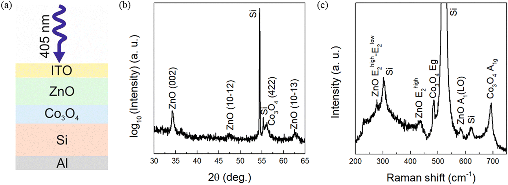 | ||
| Fig. 1 Structural characterization of the Si/Co3O4/ZnO heterojunction. (a) Illustration of the device cross section. (b) XRD pattern and (c) Raman spectrum. | ||
2.2 Computational details
First-principles calculations were performed using the projector augmented wave (PAW)18 method as implemented in the Vienna ab initio simulation package (VASP), version 6.4.2.19,20 DFT calculations were employed using the generalized gradient approximation (GGA) approximation and Perdew–Burke–Ernzerhof (PBE) functional,21 and PAW pseudopotentials with semicore states treated as valence ones for Co and Zn. The band alignment between different materials was estimated using the ionization potentials (IP) of the materials under consideration.22,23 The IP was obtained as a difference between the vacuum energy and the valence band energy maximum:| IP = ΔEvac-ref − ΔEVBM-ref | (1) |
| ECBM = EVBM + EG | (2) |
![[3 with combining macron]](https://www.rsc.org/images/entities/char_0033_0304.gif) m), imposing an A-type anti-ferromagnetic spin configuration. Then, GW calculations were performed using the same k-point grid and plane wave energy cutoff. The quasiparticle (QP) self consistent GW0 method was adopted, in which the QP eigenvalues and wave functions are both updated only in G. Corrections to QP energies due to the basis set size was performed using the infinite basis-set extrapolation procedure calculated using a 3 × 3 × 3 k-point grid.26 To obtain the potential in the vacuum region, slabs with 12 bilayers for ZnO (10−10) were used, while for Co3O4 (100) 11 layers slabs were considered. In both cases, a vacuum layer of 20 Å was used, which was thick enough to ensure convergence of the potential. The ZnO (Co3O4) slabs were relaxed until all atomic forces were smaller than 10 meV Å−1 using a γ-centered 7× 7 × 1 (5× 5 × 1) k-point grid was employed.
m), imposing an A-type anti-ferromagnetic spin configuration. Then, GW calculations were performed using the same k-point grid and plane wave energy cutoff. The quasiparticle (QP) self consistent GW0 method was adopted, in which the QP eigenvalues and wave functions are both updated only in G. Corrections to QP energies due to the basis set size was performed using the infinite basis-set extrapolation procedure calculated using a 3 × 3 × 3 k-point grid.26 To obtain the potential in the vacuum region, slabs with 12 bilayers for ZnO (10−10) were used, while for Co3O4 (100) 11 layers slabs were considered. In both cases, a vacuum layer of 20 Å was used, which was thick enough to ensure convergence of the potential. The ZnO (Co3O4) slabs were relaxed until all atomic forces were smaller than 10 meV Å−1 using a γ-centered 7× 7 × 1 (5× 5 × 1) k-point grid was employed.
3. Results and discussion
The structural characteristics of the layers in the p-Si/Co3O4/ZnO stack were investigated by XRD. The XRD pattern is shown in Fig. 1(b). The Miller indices of the diffraction peaks were successfully indexed according to the JCPDS file no.: 36-1451 (ZnO; hexagonal structure with space group P63mc and point group C6v4) and 43-1003 (Co3O4; cubic structure with space group Fdm and point group mm). In addition to the peaks from the Si substrate and the peaks from the wurzite ZnO and spinel Co3O4, no other peaks were observed, revealing the absence of secondary phases.
To further confirm the presence of the wurzite ZnO and spinel Co3O4 structures, Raman spectroscopy measurements were performed. The most dominant peak in the Raman spectrum, shown in Fig. 1(c), is located at 521 cm−1 and is connected with Ehigh2 mode of the Si substrate.27 The peaks at 301 cm−1 and 616 cm−1 are also connected with the Si substrate and detailed analyses are provided in a previous work.27 In addition, there are several typical peaks that can be assigned to the wurtzite ZnO layer as follows:28,29 277 cm−1 – Ehigh2 − Elow2, 437 cm−1 – Ehigh2, 584 cm−1 – A1(LO). Their presence confirms the structure of the ZnO layer, as well as the good quality of the layer. Two other peaks were assigned to the Co3O4 layer as follows:30–33 484 cm−1 – Eg, 693 cm−1 – A1g. The A1g peak is characteristic for the spinel structure of this layer, as it is directly connected to the Co–O breathing vibration of Co2+ ions arranged tetrahedrally.32
The optical properties of the Co3O4 thin films were evaluated. The transmittance spectrum of a Co3O4 thin film deposited on a glass substrate is shown in Fig. S1(a) (ESI†). The optical band gap (Eg) values of the films was determined by the Tauc equation:34
| (αhν)n = A(hν − Eg) | (3) |
The p-Si/Co3O4/ZnO structure was further investigated by TEM. The cross-sectional TEM image shown in Fig. 2(a) shows (from the diffraction contrast), the ZnO and Co3O4 layers deposited on the Si substrate. In addition, a native 2–3 nm thick SiOx layer was observed between the Si and the Co3O4 layers. From this cross-sectional TEM image, we obtained a thickness of approximately 70 nm for ZnO, and 15 ± 1 nm for Co3O4.
 | ||
| Fig. 2 (a) TEM image at low magnification of the Si/Co3O4/ZnO structure, (b) corresponding SAED pattern of the TEM image with four peaks indexed, (c) HRTEM image of the analyzed sample showing the interface between Si/Co3O4 and Co3O4/ZnO, (d) magnified view of the Co3O4/ZnO interface with both layers oriented relatively to the electron beam. | ||
The SAED pattern shown in Fig. 2(b) was performed on an area from the cross-sectional TEM image and consists of some intense peaks, which can be assigned to the Si substrate and some other weaker peaks arranged in diffraction rings, which can be assigned to the ZnO layer and Co3O4 layers, as indicated by the subscripts in Fig. 2(b). We indexed and assigned 5 sets of peaks corresponding to the (200)Si, (111)Si, (311)Co3O4, (400)Co3O4 and (100)ZnO crystallographic planes. All these indexed peaks belong, for the bottom layer to the spinel structure of Co3O4, a cubic structure, and for the top layer to the wurzite structure of ZnO, a hexagonal structure with space group P63mc.
Fig. 2(d) shows a HRTEM image that reveals an interfacial area, in which both ZnO and Co3O4 layers are oriented relative to the electron beam. The interface between ZnO and Co3O4 is clean and continuous, with no visible discontinuities. From the measurements performed on the HRTEM image we indexed and assigned lattice fringes to the interplanar distances corresponding to the (100)ZnO, (002)ZnO set of planes of wurzite ZnO structure and to the (311)Co3O4 set of planes of spinel structure of Co3O4, as shown in Fig. 2(d). These results are in perfect agreement with the ones measured in the SAED pattern.
In order to analyze the spatial distribution of the elements across the sample, we performed energy dispersive X-ray spectroscopy (EDS) measurements in the scanning TEM (STEM) mode. Fig. 3 shows a high-angle annular dark-field scanning transmission electron microscopy (HAADF-STEM) image, in Z-contrast mode, together with the elemental maps of Si, Co and Zn, corresponding to an area from the HAADF-STEM image. From the combined color map, which was obtained by overlapping the Si, Co and Zn maps, it is possible to observe a uniform and continuous interface between the layers with a clear delineation between them.
 | ||
| Fig. 3 High-angle annular dark-field scanning transmission electron microscopy (HAADF-STEM) image of Si/Co3O4/ZnO structure and energy dispersive X-ray spectroscopy elemental mapping performed on the HAADF-STEM image showing the spatial distribution of Zn, Co and Si elements across the analyzed STEM image. The combined color map was obtained by overlapping the Si, Co and Zn maps. | ||
The transient response of the Al/Si/Co3O4/ZnO/ITO device was investigated under no applied bias, with a 405![[thin space (1/6-em)]](https://www.rsc.org/images/entities/char_2009.gif) nm wavelength laser illumination, at a fixed power density of 251mW cm−2, as a function of the pulse repetition rate. The I–t curves shown in Fig. 4(a) display a typical sharp increase in the current when the light is turned on, and also a sharp negative peak when the light is turned off, which can be assigned to the pyroelectric effect in ZnO.35 This effect is observed at all fixed frequencies.
nm wavelength laser illumination, at a fixed power density of 251mW cm−2, as a function of the pulse repetition rate. The I–t curves shown in Fig. 4(a) display a typical sharp increase in the current when the light is turned on, and also a sharp negative peak when the light is turned off, which can be assigned to the pyroelectric effect in ZnO.35 This effect is observed at all fixed frequencies.
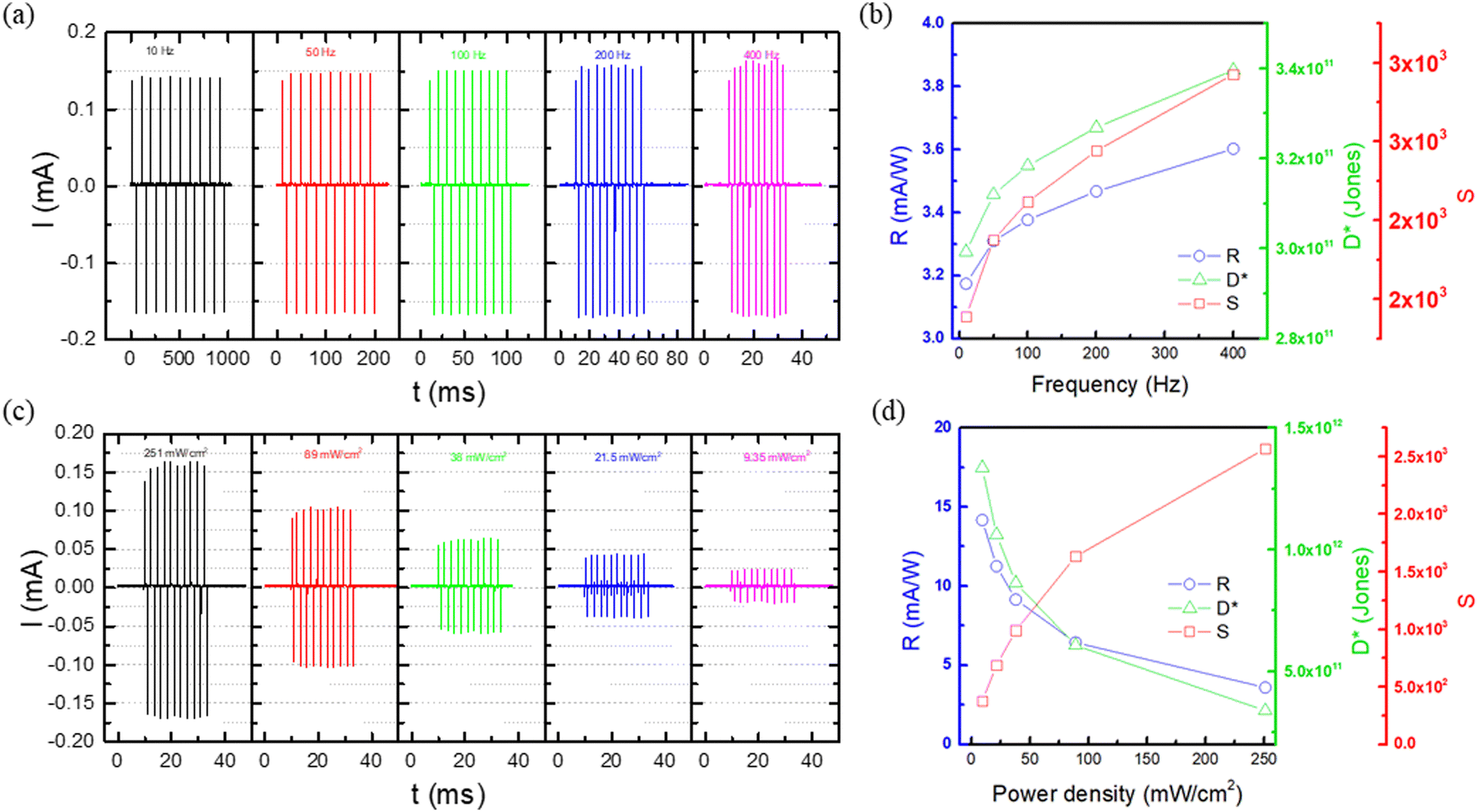 | ||
| Fig. 4 (a) I–t curves for the Al/Si/Co3O4/ZnO/ITO device at different chopper frequencies and at a fixed power density of 251 mW cm−2. (b) Variation of responsivity, detectivity and sensitivity as a function of chopper frequency. (c) I–t curves for the Al/Si/Co3O4/ZnO/ITO device at different laser power densities and at a chopper frequency of 10 Hz. (d) Variation of responsivity, detectivity and sensitivity as a function of laser power density. | ||
However, after each sharp peak, no plateau is observed. We will come back to the absence of the PV effect in these devices later. The responsivity (R), detectivity (D*), and sensitivity (S) were calculated using the equations:36,37
 | (4) |
 | (5) |
 | (6) |
nm wavelength laser illumination as a function of different laser power densities in the range of 9.35 up to 251mW cm−2, for a chopper frequency of 10Hz. The I–t curves are shown in Fig. 4(c) and it is possible to observe that they significantly change with the laser power density. Fig. 4(d) shows the variation of R, D*, S when the laser power density is decreased from 251to 9.35mW cm−2. It is possible to observe that R and D* significantly increases with decreasing power density. This is due to the fact that the ILight decreases slower than the illumination power. On the other hand, since S is only dependent on ILight and IDark, it is possible to conclude that its value decreases with decreasing power density. Therefore, a maximum R and D* of 14.2 mA W−1 and 1.34 × 10¹² Jones were achieved respectively, for a power density of 9.35mW cm−2. These values are 40% and 2 orders of magnitude higher than the ones found in the Al/Si/ZnO/ITO device.14
To further confirm the absence of the PV effect in the Al/Si/Co3O4/ZnO/ITO device, we performed current–voltage (I–V) measurements. Fig. 5(a) shows the I–V curves in the dark and with 405nm laser illumination with a power density of 9.35mW cm−2. It is possible to observe a diode-like behavior in both curves, typical from a n–p–n HJ formed at the n-Si/p-Co3O4/n-ZnO interface.36 A distinctive feature in both I–V curves is the current observed in the range −5 V to −1 V, observed in the I–V curve with laser illumination, suggesting that the device exhibits good violet light response and it is sensitive to the light intensity level. In order to confirm its impact on the PD performance, we have measured the transient response while applying an external bias to the device in the range −1 up to −5 V. Fig. 5(b) shows the I–t curves without and with external bias of −1, −2, −4 and −5 V, respectively.
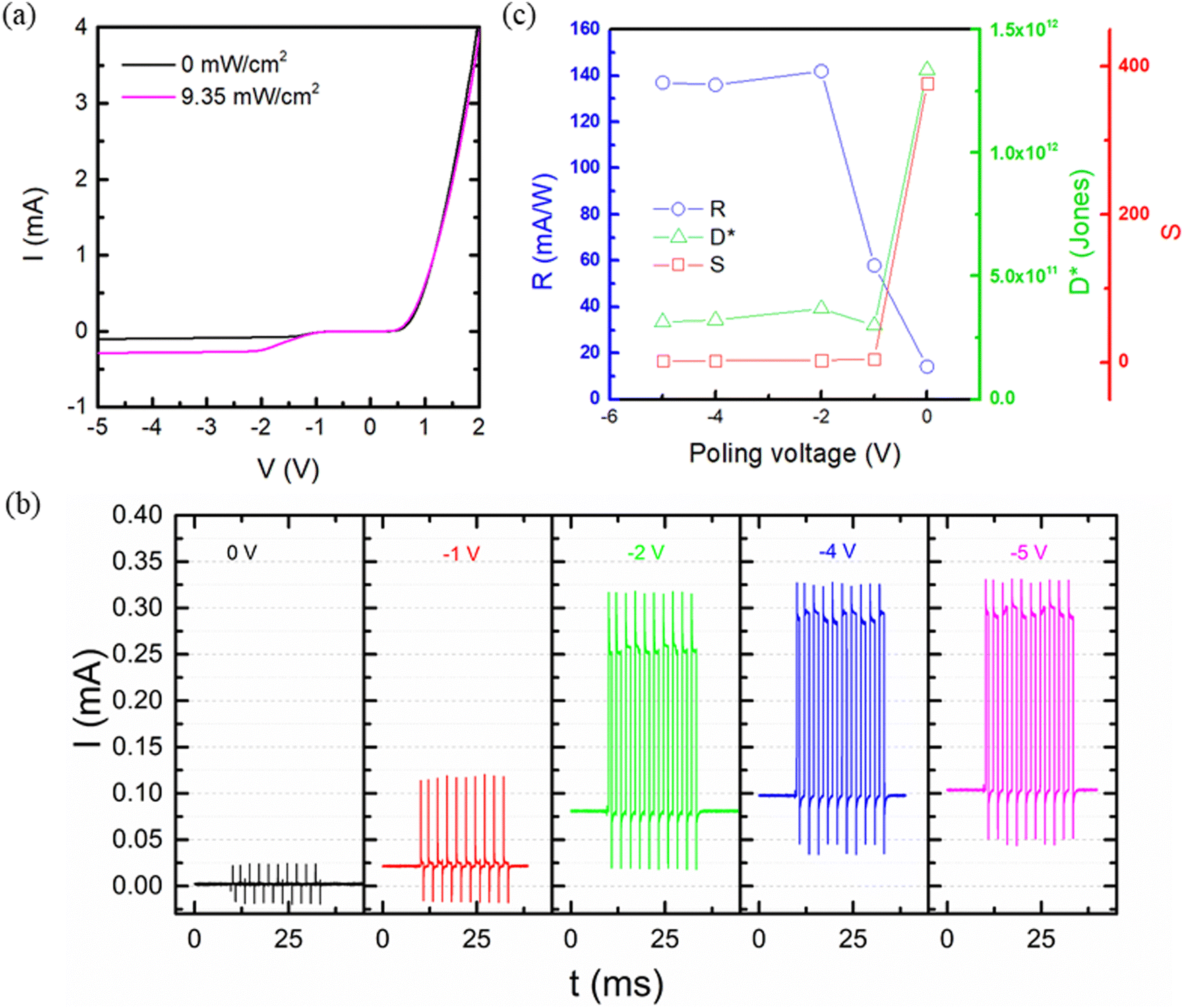 | ||
| Fig. 5 (a) I–V curves for the Al/Si/Co3O4/ZnO/ITO device in the dark and under illumination with a power density 9.35 mW cm−2. (b) I–t curves for the Al/Si/Co3O4/ZnO/ITO without and with external bias. (c) Variation of responsivity, detectivity and sensitivity as a function of external bias. | ||
It is possible to observe that the external bias has a significant effect on the response of the PD. Thus a pyro-phototronic effect takes place which can be defined as follows:36,37 under laser illumination, a sharp current peak (IPyro+PV) occurs within a short period of time due to the coupling between the pyroelectric and PV effects, the pyroelectric effect occurring due to heating from the laser. Then, under stable illumination the temperature becomes constant and the light-induced temperature gradient vanishes, and therefore the current decays from IPyro+PV to IPV. When the laser is turned off the temperature gradient in the ZnO film is now inverted and therefore a reverse current spike emerges. After the temperature gradient vanishes, the current goes back to dark current (IDark). Fig. 5(c) shows the variation of R, D*, S with the external bias. It is possible to observe that while D* and S decreases around 73 and 99.4%, respectively, the R value increases by 864% compared to the performance of the device without external bias. The decrease of D* and S are intrinsically related with the increase of IDark, as observed in Fig. 5(b), while the increase of the R value is related with the emergence of the PV effect that significantly increase ILight. In addition, the linear dynamic range (LDR), which is the light intensity range where the responsivity is maintained as a constant, was calculated as follows:38,39
 | (7) |
The LDR for the device without external bias was found to be around 52 dB of intensity linear dynamic range, which is close to the value found for other ZnO-based PDs,38,39 and also close to the value required for most imaging applications.38 However, for the device with an external bias of −2 V, the LDR was decreased to 12 dB due to the increase in the IDark.
To further understand the external bias effect, we have first performed ab initio calculations to understand which type of junction could be formed between ZnO and Co3O4 and then we have investigated the band alignment conditions under different bias conditions. Fig. 6 shows the calculated band alignments obtained considering the ionization potential, IP, of the bulk materials. The IP of ZnO was found to be 8.47 eV, and its band gap was 3.49 eV. For Co3O4, we obtained an IP of 6.17 eV, and a band gap of 1.29 eV (direct at the X point of the Brillouin zone). The band gap values agree with experimental values reported in the literature for ZnO16 and Co3O4.34 In addition, it is possible to conclude that a type II heterojunction is formed.
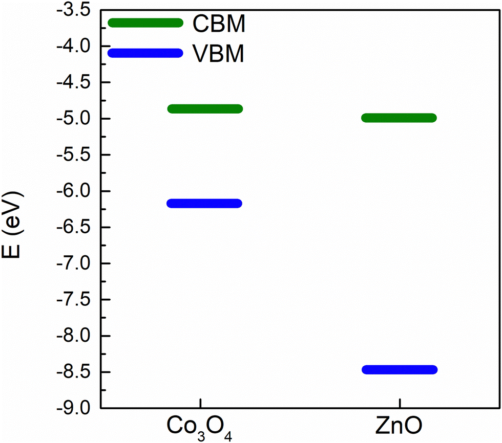 | ||
| Fig. 6 Band alignment between ZnO and Co3O4 calculated using the GW0 method. The zero of the energy corresponds to the vacuum energy. | ||
Fig. 7(a)–(f) shows the bands alignment of the investigated structure under different conditions: without external bias, with external voltages of +1 V and −2 V, while the light is turned on, and while it is shining on the sample. In the absence of bias the IPyro is present, while there is no IPV, as illustrated in Fig. 4(a) and (c). The light is absorbed in the Co3O4 layer, where the electrons are promoted to the conduction band, leaving a hole in the valence band. The electric field emerging from the pyroelectric effect in ZnO contributes to separation of the carriers, leading to the generation of the IPyro. However, in the absence of the pyroelectric field, the opposing built-in field in the n–p–n junction effectively restrains the carriers, and increases the carrier recombination. Consequently, no IPV is present in that case.
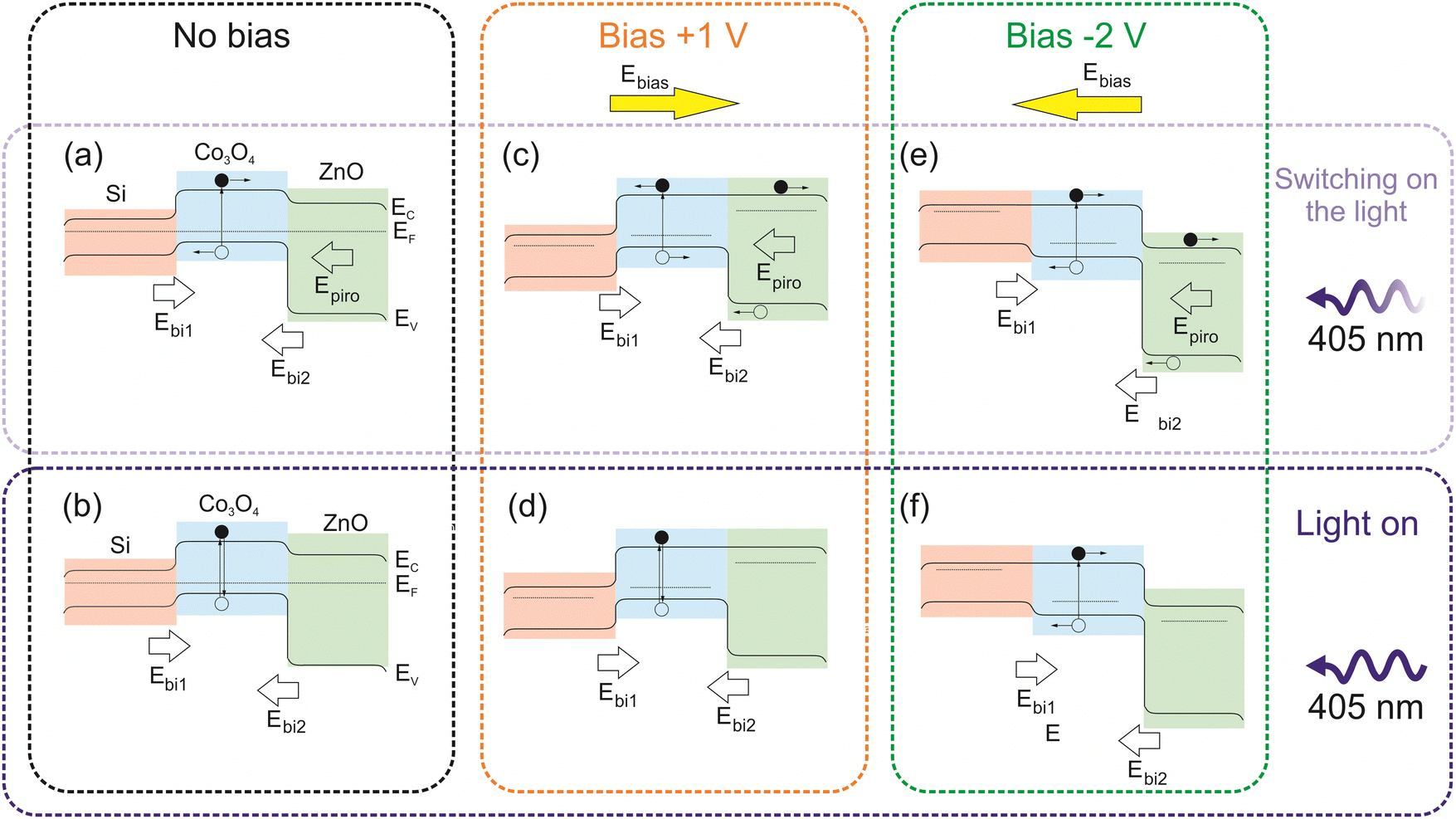 | ||
| Fig. 7 Band diagram schemes of the Si/Co3O4/ZnO structure for different conditions. (a), (c) and (e) while the light is being turned on for different bias conditions; (b), (d) and (f) with light on for different bias conditions. | ||
In the case of an external bias, the junctions are oriented in the opposite direction, resulting in the polarization of the n–p and p–n junctions being opposite. In the first scenario (Fig. 7(c) and (d)) the junction between n-Si and p-Co3O4 is polarized in the reverse direction, while the junction between p-Co3O4 and n-ZnO is polarized in the forward direction. When the light is turned on, the generated carriers are separated by the external field. However, the pyroelectric field, being in the opposite direction, restrains the carriers from effective flow. In this case, there is no current flow. While the light is shining, the pyroelectric field is no longer present. However, the external field does not separate the carriers effectively, due to the band alignment of the n–p–n junction. Consequently, there is also no current flow.
In the second scenario (Fig. 7(e) and (f)) the polarization is inverted: the junction between n-Si and p-Co3O4 is polarized in the forward direction, while the junction between p-Co3O4 and n-ZnO is polarized in the reverse direction. In this the case, the band alignment is more favorable for the flow of carriers. When the light is turned on, the pyroelectric field aligns with the field from external bias. Both of these factors contribute to the flow of the carriers, which can be observed as a current peak in Fig. 6(b). While the light is shining on the junctions, the separation of the carriers remains efficient enough to observe the photocurrent, although its value is lower than in the previous case.
We have performed cycling stability for the Al/Si/Co3O4/ZnO/ITO PDs without and with external bias of −2 V under illumination with a power density 9.35 mW cm−2 and at a chopper frequency of 100 Hz. From Fig. 8(a), it is possible to conclude that the response is stable in both cases.
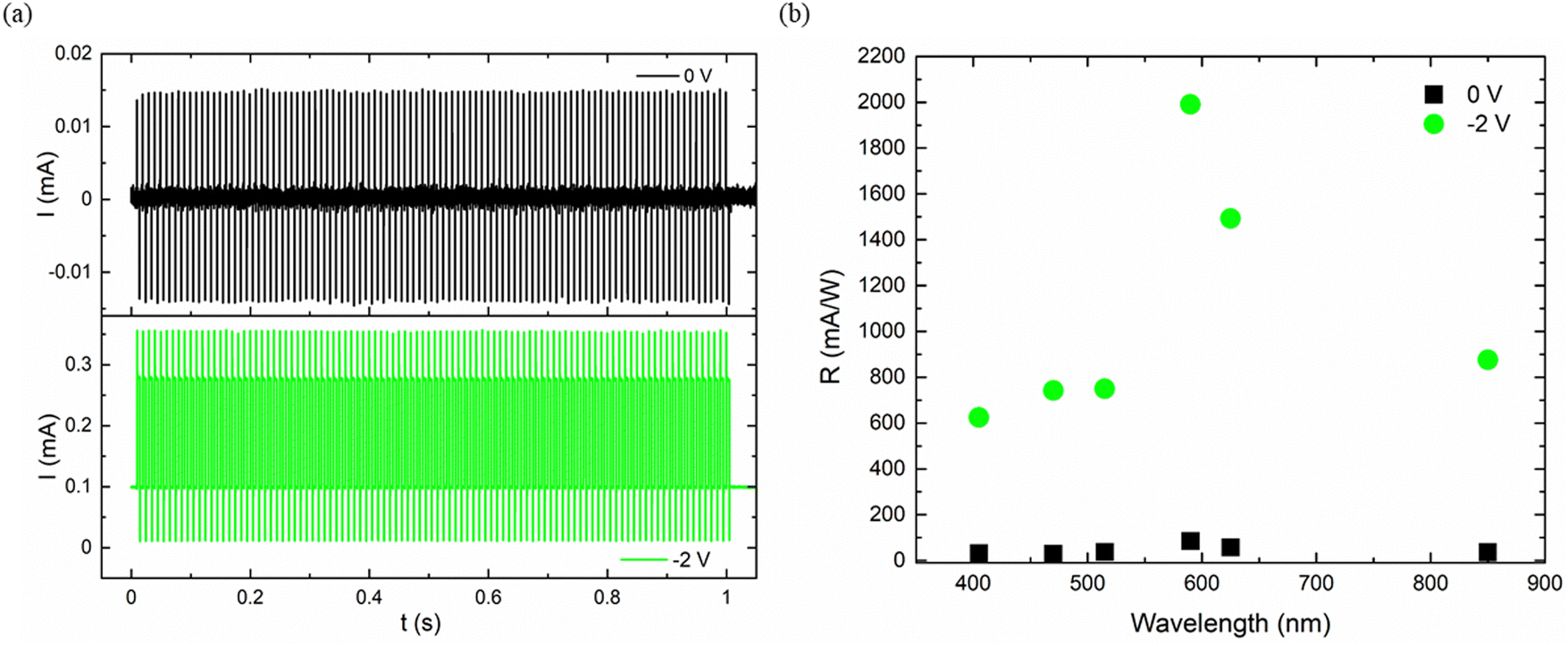 | ||
| Fig. 8 (a) Stability of the transient response characteristics of the Al/Si/Co3O4/ZnO/ITO device without and with external bias of −2 V, under illumination with 405nm laser illumination at power density 9.35 mW cm−2 and at a chopper frequency of 100 Hz. (b) Responsivity as a function of different visible incident wavelength for the Al/Si/Co3O4/ZnO/ITO device with and without external bias of −2 V measured by using light-emitting diodes with a power density of 0.25 mW cm−2. | ||
Moreover, the rise and fall times (τr and τf) were also estimated for the device with and without external bias. No significant variation was found with and without external bias and the τr and τf were found to be around 4 and 2 μs, respectively.
Table 1 shows a comparison of the R, D*, τr and τf of the PDs obtained in this work with the ones presented in the recent literature for similar excitation wavelength. For instance, compared to other n–p–n HJs, the present Al/Si/Co3O4/ZnO/ITO device exhibits very interesting features. For instance, our biased Al/Si/Co3O4/ZnO/ITO devices show a 43.5% increase in R and one order of magnitude higher D* compared to Al/Si/SnO/ZnO/ITO devices, while achieving similar τr and τf values.14 The increase in R and D* are due to the enhanced PV effect in the Al/Si/Co3O4/ZnO/ITO device. Compared to Al/Si/ZnO/NiO/Ni and ITO/NiO/ZnO/Al devices,12,13 the present Al/Si/Co3O4/ZnO/ITO devices shows much faster response times, although lower R and D* values, which is linked to the high external bias applied that needs to be applied to enhance charge carrier separation. On the other hand, compared to one of the best tri-layered HJs reported in the literature, Au/p-CuI/n-ZnO, illuminated with a UV 395 nm laser,40 our PD demonstrates a 122% increase in R, with more than an order of magnitude higher D* and at least 4 orders of magnitude decrease of τr and τf. Another advantage of our structure over CuI-based PDs is its good stability, i.e. the properties and stability of CuI-based PDs are sensitive to defects.41
| Structure | Power density (mW cm−2) | Wavelength (nm) | Bias (V) | R (mA W−1) | D* (Jones) | τ r (μs) | τ f (μs) | Ref. |
|---|---|---|---|---|---|---|---|---|
| Al/Si/SnOx/ZnO/ITO | 36 | 405 | 0 | 36.7 | 1.5 × 10¹¹ | 3 | 2 | 36 |
| Al/Si/SnO/ZnO/ITO | 36 | 405 | 0 | 93 | 3.1 × 10¹⁰ | 2 | 2 | 14 |
| Ag/ZnO/CuI/Ag | 0.28 | 395 | 0 | 17.7 | 5 × 10⁹ | 4.1 × 10⁵ | 2.4 × 10⁵ | 40 |
| Ag/ZnO/CuI/Au/Ag | 0.28 | 395 | 0 | 61.5 | 1.7 × 10¹⁰ | 4.1 × 10⁵ | 8 × 10⁴ | 40 |
| Al/Si/ZnO/NiO/Ni | 1.1 × 10⁻³ | 280 | −7 | 9.4 × 10³ | 3 × 10¹³ | 10.5 × 10⁶ | 8.3 × 10⁵ | 12 |
| ITO/NiO/ZnO/Al | 110 | 280 | 4 | >104 | 9.3 × 10¹⁴ | — | — | 13 |
| Al/Si/Co3O4/ZnO/ITO | 9.35 | 405 | 0 | 14.2 | 1.34 × 10¹² | 4 | 2 | This work |
| Al/Si/Co3O4/ZnO/ITO | 9.35 | 405 | −2 | 142 | 3.6 × 10¹¹ | 4 | 2 | This work |
We also have measured R versus different visible incident wavelength for the Al/Si/Co3O4/ZnO/ITO device with and without external bias of −2 V, as shown in Fig. 8(b), by using light-emitting diodes with a power density of 0.25 mW cm−2. It is possible to observe that the present PDs show remarkable photodetection properties, at low power densities, for different visible incident wavelengths confirming the promising characteristics of the Al/Si/Co3O4/ZnO/ITO devices.
4. Conclusions
We demonstrate that Al/Si/Co3O4/ZnO/ITO devices are promising as stable photodetectors operating in the visible wavelength range. The photoresponse of the Al/Si/Co3O4/ZnO/ITO device to 405 nm laser illumination has been systematically examined as a function of the chopper frequency and incident light power density. The photodetector performance is attributed to the pyroelectric effect in the ZnO film with chopper frequency having a negligible effect on performance. It was found that a decrease of power density produces a significant increase in responsivity and detectivity, due to the fact that the generated current decreases more slowly than the illumination power. Moreover, the biased photodetector shows a decrease in detectivity and sensitivity compared to the unbiased device (by around 73 and 99.4%, respectively) because of the increase in the dark current. On the other hand, the responsivity drastically increases by a factor of 10. Careful analysis of the band diagrams reveal that biasing is an effective way towards enhancing the photovoltaic effect that, coupled with the pyroelectric effect, causes the performance enhancement. In addition, the rise and fall times were found to be around 4 and 2 μs, respectively. Overall, by using novel tri-layered heterojunctions made of simple binary oxides, photodetectors with high responsivity and ultrafast response times are demonstrated, outperforming in terms of responsivity and response times, other tri-layered heterojunctions made of less stable p-type materials, such as SnOx and CuI.Conflicts of interest
The authors declare no conflict of interest.Acknowledgements
This work was supported by: (i) the Portuguese Foundation for Science and Technology (FCT) in the framework of the Strategic Funding Contracts UIDB/04650/2020; (ii) the exploratory research project 2022.01740.PDTC (https://doi.org/10.54499/2022.01740.PTDC) and (iii) the project M-ERA-NET3/0003/2021 – NanOx4EStor grant agreement no 958174 (https://doi.org/10.54499/M-ERA-NET3/0003/2021). J. P. B. S. also thanks FCT for the contract under the Institutional Call to Scientific Employment Stimulus – 2021 Call (CEECINST/00018/2021). The authors would like also to thank engineer José Santos for technical support at the Thin Film Laboratory and Eunika Zielony, PhD, for technical support with Raman measurements. K. G. acknowledges support from the National Science Centre in Poland grant no. 2023/07/X/ST7/00073. M. C. I. and C. G. acknowledge the financial support by a grant of the Ministry of Research, Innovation and Digitization, CNCS/CCCDI – UEFISCDI, project number COFUND-M-ERANET-3-NanOx4Estor, within PNCDI III. JLM-D. and R. L. Z. H. thank the EPSRC for support (grant no. EP/P007767/1 [CAM-IES] and no. EP/Y032942/1). J. L. M-D. acknowledges support from the Royal Academy of Engineering Chair in Emerging Technologies scheme (no.: CIET1819_24) and the ERC advanced grant, EU-H2020-ERC-ADG no. 882929, EROS, and the EPSRC grant no. EP/Y032942/1.References
- S. Sahare, P. Ghoderao, M. K. Sharma, M. Solovan, R. Aepuru, M. Kumar, Y. Chan, M. Ziółek, S.-L. Lee and Z.-H. Lin, Nano Energy, 2023, 107, 108172 CrossRef CAS
.
- J. P. B. Silva, E. M. F. Vieira, K. Gwozdz, N. E. Silva, A. Kaim, M. C. Istrate, C. Ghica, J. H. Correia, M. Pereira, L. Marques, J. L. MacManus-Driscoll, R. L. Z. Hoye and M. J. M. Gomes, Mater. Horiz., 2024, 11, 803–812 RSC
- L. Guo, H. Wang, Z. Xu, R. Cong, L. Zhao, S. Zhang, K. Zhang, L. Gao, S. Wang, C. Pan and Z. Yang, Adv. Funct. Mater., 2023, 33, 2306526 CrossRef CAS
- A. R. Jayakrishnan, J. P. B. Silva, K. Gwozdz, M. J. M. Gomes, R. L. Z. Hoye and J. L. MacManus-Driscoll, Nano Energy, 2023, 118(Part A), 108969 CrossRef CAS
-
Z. L. Wang, Y. Zhang and W. Hu, Pyro-phototronic Effect, Piezotronics and Piezo-Phototronics. Microtechnology and MEMS, Springer, Cham, 2023 DOI:10.1007/978-3-031-31497-1_18
- Z. Wang, R. Yu, C. Pan, Z. Li, J. Yang, F. Yi and Z. L. Wang, Nat. Commun., 2015, 6, 8401 CrossRef CAS PubMed
- V. Panwar, S. Nandi, M. Majumdera and A. Misra, J. Mater. Chem. C, 2022, 10, 12487–12510 RSC
- B. Wang, Y. Zhu, J. Dong, J. Jiang, Q. Wang, S. Li and X. Wang, Nano Energy, 2020, 70, 104544 CrossRef CAS
- X. Wang, Y. Dai, R. Liu, X. He, S. Li and Z. L. Wang, ACS Nano, 2017, 11, 8339–8345 CrossRef CAS PubMed
- W. Ouyang, J. Chen, Z. Shi and X. Fang, Appl. Phys. Rev., 2021, 8, 031315 CAS
- B. Yin, H. Zhang, Y. Qiu, Y. Luo, Y. Zhao and L. Hu, Nanoscale, 2017, 9, 17199–17206 RSC
- J.-D. Hwang and B.-W. Cheng, IEEE Sens. J., 2023, 23, 15523 CAS
- J.-D. Hwang, Y.-E. Hwang and Y.-A. Chen, Nanotechnology, 2021, 32, 405501 CrossRef CAS PubMed
- E. M. F. Vieira, J. P. B. Silva, K. Gwozdz, A. Kaim, N. M. Gomes, A. Chahboun, M. J. M. Gomes and J. H. Correia, Small, 2023, 19, 2300607 CrossRef CAS PubMed
- R. Balakarthikeyan, A. Santhanam, K. Vibha, M. Shkir, H. Algarni, I. M. Ashraf, M. Kumar and M. R. V. Reddy, Surf. Interfaces, 2023, 38, 102849 CrossRef CAS
- J. P. B. Silva, K. C. Sekhar, F. Cortés-Juan, R. F. Negrea, A. C. Kuncser, J. P. Connolly, C. Ghica and J. Agostinho Moreira, Sol. Energy, 2018, 167, 18–23 CrossRef CAS
- J. P. B. Silva, K. Gwozdz, L. S. Marques, M. Pereira, M. J. M. Gomes, J. L. MacManus-Driscoll and R. L. Z. Hoye, Carbon Energy, 2023, 5, e297 CrossRef CAS
- P. E. Blöchl, Phys. Rev. B: Condens. Matter Mater. Phys., 1994, 50, 17953–17979 CrossRef PubMed
- G. Kresse and J. Furthmüller, Phys. Rev. B: Condens. Matter Mater. Phys., 1996, 54, 11169–11186 CrossRef CAS PubMed
- G. Kresse and D. Joubert, Phys. Rev. B: Condens. Matter Mater. Phys., 1999, 59, 1758–1775 CrossRef CAS
- J. P. Perdew, K. Burke and M. Ernzerhof, Phys. Rev. Lett., 1996, 77, 3865–3868 CrossRef CAS PubMed
- Y. Hinuma, F. Oba, Y. Kumagai and I. Tanaka, Phys. Rev. B: Condens. Matter Mater. Phys., 2013, 88, 035305 CrossRef
- Y. Hinuma, A. Grüneis, G. Kresse and F. Oba, Phys. Rev. B: Condens. Matter Mater. Phys., 2014, 90, 155405 CrossRef
- G. Onida, L. Reining and A. Rubio, Rev. Mod. Phys., 2002, 74, 601–659 CrossRef CAS
- R. Starke and G. Kresse, Phys. Rev. B: Condens. Matter Mater. Phys., 2012, 85, 075119 CrossRef
- J. Klimeš, M. Kaltak and G. Kresse, Phys. Rev. B: Condens. Matter Mater. Phys., 2014, 90, 075125 CrossRef
- B. Yang, A. Kumar, P. Feng and R. S. Katiyar, Appl. Phys. Lett., 2008, 92, 233112 CrossRef
- R. Cuscó, E. Alarcón-Lladó, J. Ibáñez, L. Artús, J. Jiménez, B. Wang and M. J. Callahan, Phys. Rev. B: Condens. Matter Mater. Phys., 2007, 75, 165202 CrossRef
- E. Zielony, A. Wierzbicka, R. Szymon, M. A. Pietrzyk and E. Placzek-Popko, Appl. Surf. Sci., 2021, 538, 148061 CrossRef CAS
- S. K. J. Vijitha, K. Mohanraj and R. P. Jebin, Chem. Phys. Impact, 2023, 6, 100143 CrossRef
- R. Edla, N. Patel, M. Orlandi, N. Bazzanella, V. Bello, C. Maurizio, G. Mattei, P. Mazzoldi and A. Miotello, Appl. Catal., B, 2015, 166–167, 475–484 CrossRef CAS
- S. G. Victoria, A. M. Ezhil Raj and C. Ravidhas, Mater. Chem. Phys., 2015, 162, 852–859 CrossRef CAS
- V. G. Hadjiev, M. N. Iliev and I. V. Vergilov, J. Phys. C: Solid State Phys., 1988, 21, L199–L201 CrossRef
- H. El Aakib, J. F. Pierson, M. Chaik, C. S. Vall, H. A. Dads, A. Narjis and A. Outzourhit, Vacuum, 2019, 159, 346–352 CrossRef CAS
- W. Peng, Z. Pan, F. Li, Y. Cai and Y. He, Nano Energy, 2020, 78, 105268 CrossRef CAS
- J. P. B. Silva, E. M. F. Vieira, K. Gwozdz, A. Kaim, L. M. Goncalves, J. L. MacManus-Driscoll, R. L. Z. Hoye and M. Pereira, Nano Energy, 2021, 89(Part A), 106347 CrossRef CAS
- Z. Wang, R. Yu, X. Wang, W. Wu and Z. L. Wang, Adv. Mater., 2016, 28, 6880–6886 CrossRef CAS PubMed
- Z. Jin, L. Gao, Q. Zhou and J. Wang, Sci. Rep., 2014, 4, 4268 CrossRef PubMed
- R. Jalal, K. Ozel, A. Atilgan and A. Yildiz, Nanotechnology, 2024, 35, 265705 CrossRef PubMed
- F. Cao, L. Jin, Y. Wu and X. Ji, J. Alloys Compd., 2021, 859, 158383 CrossRef CAS
- K. Zhang, S. W. Wang and L. X. Yi, Opt. Mater., 2022, 134(Part A), 113204 CrossRef CAS
Footnote |
| † Electronic supplementary information (ESI) available. See DOI: https://doi.org/10.1039/d4tc01624f |
| This journal is © The Royal Society of Chemistry 2024 |