Scalable slot-die coating of high performance perovskite solar cells†
James B.
Whitaker
,
Dong Hoe
Kim
,
Bryon W.
Larson
,
Fei
Zhang
 ,
Joseph J.
Berry
 ,
Maikel F. A. M.
van Hest
* and
Kai
Zhu
 *
*
National Renewable Energy Laboratory, Golden, Colorado 80401, USA. E-mail: Maikel.van.Hest@nrel.gov; Kai.Zhu@nrel.gov
First published on 3rd August 2018
Abstract
Perovskite based photovoltaic devices hold the promise to greatly reduce the cost of solar energy production; however, this potential depends greatly on the ability to deposit perovskite active layers using large scale deposition methods such as slot-die coating without sacrificing efficiency. Using a perovskite precursor ink with long wet-film processing window, we demonstrate efficient perovskite solar cells based on slot-die coated perovskite layer. We found almost no difference in the photophysical and structural details of perovskite films that were deposited by spin coating to films deposited by slot-die coating. We explored various slot-die coating parameters to determine their effect on the performance of the device metrics. In addition to slot-die coating, we demonstrate the versatility of this wide wet-film processing window by fabricating perovskite solar cells with active layers deposited by spin coating, blade coating, and spray coating that all exhibited similar performance.
Introduction
Polycrystalline thin film solar cells based on organic–inorganic hybrid halide perovskites have reached a certified power conversion efficiency (PCE) of 22.7% in less than a decade of research.1 In spite of the fact that several challenges remain to be addressed, such as device stability, there has been a rapid escalation of interest in scaling up perovskite solar cells (PSCs) towards the fabrication of modules as a potential future PV technology.2 Various scalable deposition approaches have been tested for perovskite solar cells and/or modules development. These approaches include screen printing, blade coating, spray coating, chemical vapor phase deposition, slot-die coating, and inkjet printing.3,4 Among various scalable coating techniques, slot-die coating is one of the attractive techniques due to its potential coating uniformity across large areas, high throughput with the ability to coat at speeds greater than 600 m min−1, high material utilization with little waste, as well as the ability to be integrated into both sheet-to-sheet (S2S) and roll-to-roll coating (R2R) systems.5–7 In addition, the film thicknesses can be controlled by varying the precursor concentration, solution precursor feed rate, gap height, and coating speed. Notwithstanding these potential advantages, there are still numerous challenges that must be overcome inorder to obtain continuous and stable thin perovskite films. Owing to the fact that small disturbances in gap height or impurities can disrupt or break up the liquid film, the progress of using slot-die coating for large-scale PSC development seems to lag behind. This conclusion is based on a handful of studies with different device architectures on rigid or flexible substrates using one-step or two-step perovskite deposition.8–15 The device performance has reached up to about 11% for flexible substrate13 and over 14% for glass substrate.8 The challenge generally lies in the control of the perovskite film drying and crystal growth process during slot-die coating. Gas quenching with N2 flow and/or using a heated substrate or ultrasonic substrate vibration to increase the drying speed, or adjusting precursor composition to induce faster crystallization of perovskite layers have been tested for improving perovskite film coverage and crystallization.12,15–17Here, we demonstrate a slot-die coated perovskite device achieving 18% reverse J–V sweep PCE. This device was fabricated with a customized Coatema Easycoater slot-die coating station at room temperature and in ambient conditions. We used a robust perovskite precursor with a wide processing window of up to 20 minutes between film deposition and antisolvent dipping. Importantly, this wide processing window opens the door for large scale coating methods that are amendable toward high throughput roll-to-roll coating of PSC devices. We further demonstrate the utility of this wide processing window for PSC fabrication using four different thin film deposition techniques including slot-die, spin coating, blade coating, and spray coating. Remarkably, a similar reverse J–V sweep PCE was achieved for each deposition technique signifying the importance of developing perovskite precursor ink for scalable PSC fabrication.
Results and discussion
Optimization of coating parameters for film thickness control and coverage
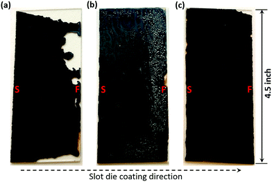
Sheet-to-sheet slot-die coating is a non-contact coating method based on pumping a precursor solution through a die with a well-defined slit as shown in Fig. 1. The die-head is then passed over the substrate at a set coating speed. The film thickness can be controlled by adjusting the coating speed, precursor solution flow rate, the gap spacing between the slot-die head and substrate, as well as the precursor solution concentration.18 Achieving a homogeneous and defect free slot-die coated film relies on the formation of a steady state meniscus between the slot-die head and the substrate. In general, the breakdown of this steady state meniscus during slot-die coating will result in various defects including incomplete coverage or pinching in, poor thickness control, ribbing, streaking, and bubbles.19,20 Many of these defects are caused by a mismatch of solution supply (the precursor flow rate) and demand (the coating speed). The coating speed and precursor solution flow rate were adjusted until a uniform thin film was achieved. When the flow rate of the precursor solution was not sufficient, the meniscus started to break down and pinch in (Fig. 2a). As the meniscus breaks down the film also becomes progressively thinner in the direction of coating. The film thickness in Fig. 2a was measured using profilometry and decreased from over 600 nm, where coating was initiated (the point marked “S” in Fig. 2a), down to less than 400 nm where the meniscus was breaking down at the end of the coating (the point marked “F” in Fig. 2a). Conversely, when the flow rate was too high, as seen in Fig. 2b, the meniscus begins to swell resulting in severe thickness variations and an overall thickening of the finished film. The film in Fig. 2b increased from about 680 nm at the beginning of coating to over 1 μm in the direction of coating. At film thicknesses of greater than 1 μm, the film starts to crack and bubble during annealing resulting in the textured surface that is visible in Fig. 2b. When the solution precursor supply matches up with the deposition rate, as shown in Fig. 2c, a steady state meniscus is formed and the resulting film is homogeneous across as well as down the length of the substrate. The thickness of the film 2c only slightly decreased from about 580 nm down to 560 nm. This slight decrease could be further minimized by additional fine tuning of flow rate and coating speed.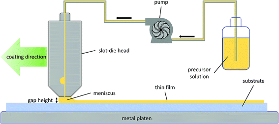 | ||
| Fig. 1 Schematic illustration of the key steps involved in slot-die coating of perovskite thin films. | ||
Effect of slot-die coating parameters on perovskite device performance
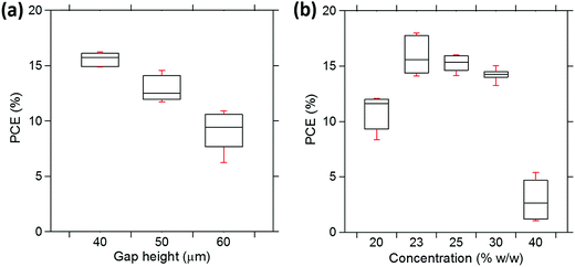
As the gap height between the slot-die head and substrate is increased the resulting film becomes thicker. This effect was demonstrated by depositing different films and progressively increasing the gap height from 40 μm to 50 μm to 60 μm while all other parameters were kept constant. The resulting film thickness increased from 457 ± 7 nm to 563 ± 5 nm to 647 ± 5 nm respectively. To optimize the gap height and to determine the optimal film thickness for PSC devices, the same series of gap heights were used to slot-die coat perovskite layers for functional devices. The impact of varying the gap height, all other parameters were kept constant, on the performance of PSCs made by slot-die coating are presented in Fig. 3. These devices were prepared by spin coating both the SnO2 and spiro-OMeTAD layers as experimental controls for comparison to literature results. The perovskite layer was deposited by slot-die coating in ambient conditions with the relative humidity between 25–35%. It is generally known that the relative humidity can strongly affect device performance,21 adding further support to the robustness of this ink system. The device architecture for all devices is ITO/SnO2/MAPbI3/spiro-OMeTAD/Au. As the perovskite film thickness increases, the median reverse sweep PCE begins to decrease from about 15.7% to 12.5% to 9.4%. As expected, the corresponding open-circuit voltage (Voc) and fill factor (FF) also decrease (Fig. S1 in ESI†). The short-circuit current density (Jsc) increases from 21 mA cm−2 to 21.7 mA cm−2 as the gap is increased from 40 μm to 50 μm respectively. When the gap is further increased to 60 μm, the Jsc is the same at a 99% confidence interval.In addition to changing the gap height, increasing the perovskite precursor concentration was also shown to increase the resulting film thickness. Five different perovskite precursor concentrations but identical compositions were prepared: 20% w/w, 23% w/w, 25% w/w, 30% w/w, and 40% w/w. These five different precursor concentrations were used to slot-die coat five different films using the same flow rate and same gap height. These films were then measured with a profilometer and determined to be about 336 ± 14 nm, 431 ± 9 nm, 455 ± 6 nm, 549 ± 7 nm, and >1 μm respectively. These same solutions and slot-die coating parameters were then used to fabricate PSC devices. The performance of these devices are presented in Fig. 3b. The corresponding Voc, Jsc, and FF are shown in Fig. S2 in ESI.† The devices prepared from the 20% w/w exhibits a low average Jsc of 18.6 ± 0.4 mA cm−2 compared to the thicker devices prepared from the 25% w/w averaging 21.7 ± 0.3 mA cm−2. This observation suggests that the film deposited from 20% w/w is too thin. The current density from the devices prepared from 23% w/w, 25% w/w and 30%w/w are the same within a 99% confidence interval. Owing to the fact that the current density does not increase going from 23% w/w to 25% w/w up to 30% w/w, we considered the film deposited from 23% w/w to be the optimum concentration for this composition and device architecture. The decrease in performance when moving from 23% w/w to 25% w/w to 30% w/w is due to a slight decrease in average Voc from 1.07 ± 0.02 V to 1.0 ± 0.04 V to 0.91 ± 0.02 V respectively. As the concentration of the precursor is increased to 40% w/w, the resulting film becomes extremely thick (>1 μm) with numerous cracks, pinholes, surface texture and ultimately in a low performing device.
Film characterization and comparison
Perovskite precursors22,23 based on solvent tuning along with the use of methylammonium chloride (MACl) has been shown to increase the process window between deposition and anti-solvent dipping by up to 8 min for PSC fabrication. This increased process window is a key component toward moving from spin coating toward large scale deposition techniques such as slot-die coating. This increased processing window is especially important on a roll-to-roll system due to the inherent delay between the coating station and a secondary station for anti-solvent dipping or thermal annealing. To determine to what effect, if any, moving from spin coating to slot-die coating has on the resulting films, several characterization methods were used to compare spin coated films to slot-die coated films.The morphology of the slot-die coated film was examined by SEM. The cross-section and top views of slot-die coated perovskite thin film is shown in Fig. 4. The film consist of grains spanning the entire film thickness. This is attractive for collecting charges across the film thickness. The top view SEM images indicate that the slot-die coated film is compact with minimum pinholes. The average grain size is about 1.5 μm. The grain size of the film is comparable to that prepared by spin coating with the same precursor ink (Fig. S3 in ESI†). This is a striking result considering for spin coated films most of solvent was removed during spin coating before being submerged in the anti-solvent bath whereas for the slot-die coated film all the solvent was allowed to dry in ambient conditions for several minutes prior to being submerged in the anti-solvent bath. The observation that the grain size and morphology of the slot-die coated film is so similar to films deposited by spin coating indicates that this precursor exhibits a long processing window as well as a wide tolerance for various drying conditions. In addition to microscopy, X-ray diffraction (XRD) and ultraviolet-visible (UV-vis) absorption spectroscopy were used to study the structural and optical properties the slot-die coated film. These results are shown in Fig. S4 (XRD) and Fig. S5† (UV-vis), respectively.
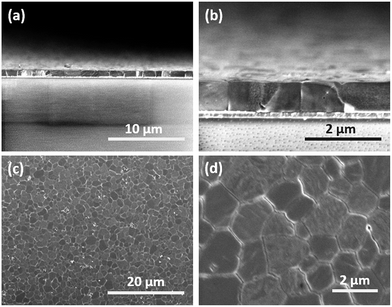 | ||
| Fig. 4 Scanning electron microscopy (SEM) images of (a and b) cross-section view and (c and d) top view of slot-die coated perovskite thin films. | ||
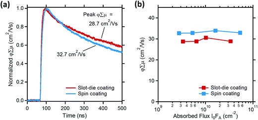
Time-resolved microwave conductivity (TRMC) measurements were conducted to examine the photophysical properties of perovskite thin films. TRMC is a useful technique for characterizing device-relevant charge carrier dynamics in PV thin films (refer to the experimental section for details of the measurement, and to the literature24,25 for more in-depth discussions of the technique). TRMC is especially powerful for evaluating a thin film's intrinsic PV potential since the measurement is carried out in the absence of any metal contacts or interfacial layers that may otherwise convolute the results, such as in the case of devices. The two primary figures of merit from TRMC are the carrier yield-mobility product and the average carrier lifetime. In high performance MAPbI3 thin films, the free carrier generation yield is typically 1,26 therefore the carrier yield-mobility product figure (ϕ∑μ) can simply be regarded as a measure of carrier mobility (Fig. 5).
The slot-die and spin coated MAPbI3 films (both films deposited on bare glass) were measured by TRMC using an excitation wavelength of 650 nm to ensure bulk generation of charges throughout the film.27 The peak ϕ∑μ values were 28.7 and 32.7 cm2 V−1 s−1 for the slot-die and spin coated films, respectively, consistent with values reported for other spin-coated MAPbI3 films, and higher than mobilities reported for vapor deposited films.28 Bi-exponential fits of the photoconductivity transients revealed similar average free carrier lifetimes of ∼530 ns for the slot-die coated film and ∼630 ns for the spin coated film. Mobility values extracted from TRMC measurements represent local carrier mobilities, and therefore are typically higher than bulk mobilities measured by space charge limited current (SCLC) or time of flight, where grain boundaries and other transport barriers are also sampled. Nonetheless, if we assume that free carriers in these MAPbI3 films obey Boltzmann statistics, then an upper boundary on the carrier diffusion coefficient, Dc, can be estimated using the local mobility, μ, and Einstein's carrier diffusion relationship:
From the carrier diffusion coefficient, an upper limit on the carrier diffusion length, LD, can be calculated by:
These TRMC results correspond to carrier diffusion lengths of 6.3 and 7.3 microns, respectively, for the slot-die and spin coated MAPbI3 films, indicating that a film thickness of several hundred nanometers (produced by either coating technique) should not be a limiting factor on Jsc even if the local and bulk carrier mobilities differ by as much as an order of magnitude (Fig. 6).
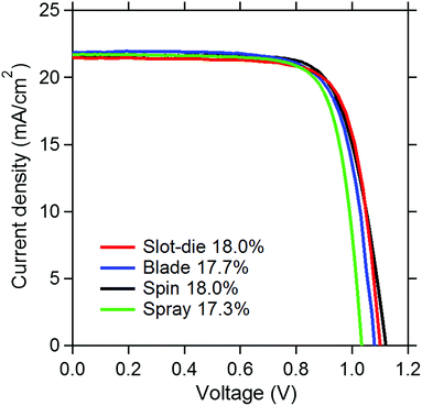 | ||
| Fig. 6 J–V curves of PSCs fabricated with the perovskite layer deposited by slot-die coating (red), blade coating (blue), spin coating (black), and spray coating (green). The device architecture is glass/ITO/SnO2/MAPbI3/spiro-OMeTAD/Au. The J–V curve for spray coating reproduced from Uličná et al. with permission.29 | ||
Fabrication of PSCs with different coating techniques
Four different PSC devices were fabricated using four different methods to deposit the perovskite layer using the same perovskite precursor ink: spin coating, blade coating, spray coating, and slot-die coating. The spray coating data was reproduced from our previous study.29 All four devices showed very similar performance characteristics as shown in Table 1. Both reverse-scan and forward-scan J–V curves are shown in Fig. S6 (ESI†). These devices exhibited hysteresis behavior as often observed for planar n-i-p perovskite solar cells. Stable power outputs (SPOs) of these devices were performed near their maximum power points. The SPO results are also shown in Fig. S6.† The SPOs are similar among these devices and are around 15%. It is noteworthy that modifying the contact layer (e.g., electron transport layer treatment with PCBM) can increase the forward scan J–V efficiency, leading to overall improved SPO;22 this will be a subject of future optimization study. Despite the existence of hysteresis, the similar J–V and SPO results among different coating methods are exciting in the context of vastly different film drying mechanisms between the various deposition techniques and consequently the vastly different perovskite crystallization dynamics. For example, during spin coating the solvent evaporation rate is faster while the substrate is spinning whereas during slot-die coating the solvent evaporation takes a much longer time. Due to the high boiling point of the solvent coupled with MACl slowing down crystal growth,30 the perovskite crystal formation between the different coating methods appears to be similar. Remarkably, with the optimization of gap height, coating speed, and precursor concentration we were able to obtain an PSC with reverse J–V sweep PCE 18% (SPO of ∼15.6%) with a slot-die coated perovskite layer.It is worth noting for the devices that were slot-die coated, it was necessary to include a delay time in-between coating and antisolvent dipping. This delay time is not necessary for spin coated devices due to the fast solvent evaporation rate while the substrate is spinning. The reverse sweep PCE of devices fabricated with a slot-die coated perovskite layer increased from <6% up to 18% when the delay between coating and anti-solvent dipping was increased from less than 15 seconds to 5 min (Fig. S7 in ESI†). This delay time when slot-die coating can be affected by coating temperature, precursor concentration, substrate size, and deposition temperature, which likely will alter solvent evaporation rate for the slot-die coated precursor film.
Conclusions
In summary, we have demonstrated a perovskite solar cell containing a slot-die coated active layer that achieved 18% reverse J–V sweep PCE. Achieving a high efficiency perovskite solar cell by slot-die coating is an important step toward realizing the goal of large scale high-throughput commercial production of inexpensive mixed halide perovskite based solar cells. We were able to achieve this result by using a precursor solution with long wet film processing time window. To confirm that the slot-die coated films were photophysically and morphologically the same as the spin coated films, we conducted TRMC, UV-vis spectroscopy, XRD, and SEM; we found there to be no significant differences between the two films. Furthermore, we have also shown how versatile and robust this perovskite precursor is by demonstrating four different devices with four different thin film coating techniques, slot-die coating, spin coating, blade coating, and spray coating, with comparable device performance.Experimental
Materials
All materials were used as received without any further purification unless otherwise stated. The tin(IV) oxide 15% w/v in H2O colloidal dispersion was purchased from Alfa Aesar. Methylammonium iodide (MAI) was purchased from Dyesol. Methylammonium hydrochloride (MACl ≥ 98%), N,N-dimethylformamide (DMF 99.8% anhydrous), N-methyl-2-pyrrolidone (NMP 99.5%), 4-t-butylpyridine (TBP 96%), acetonitrile (AcN 99.8% anhydrous), lithium bis(trifluoromethane)sulfonimide salt (LiTFSI 99.95%), and chlorobenzene (CB 99.8% anhydrous) were all purchased from Sigma Aldrich. Diethylether (DEE 99.9% with 8 ppm BHT stabilized) was purchased from Fisher Scientific. Lead iodide (PbI2 99.99%) was purchased from TCI. 2,2′,7,7′-tetrakis(N,N′-dimethoxyphenylamine)-9,9′-spirobifluorene (spiro-OMeTAD) was purchased from Merck.Perovskite film deposition
Spin coated perovskite films were deposited from a 40.2% w/w solution with a molar ratio of 1![[thin space (1/6-em)]](https://www.rsc.org/images/entities/char_2009.gif) :
:![[thin space (1/6-em)]](https://www.rsc.org/images/entities/char_2009.gif) 1.1
1.1![[thin space (1/6-em)]](https://www.rsc.org/images/entities/char_2009.gif) :
:![[thin space (1/6-em)]](https://www.rsc.org/images/entities/char_2009.gif) 0.15 (MAI
0.15 (MAI![[thin space (1/6-em)]](https://www.rsc.org/images/entities/char_2009.gif) :
:![[thin space (1/6-em)]](https://www.rsc.org/images/entities/char_2009.gif) PbI2
PbI2![[thin space (1/6-em)]](https://www.rsc.org/images/entities/char_2009.gif) :
:![[thin space (1/6-em)]](https://www.rsc.org/images/entities/char_2009.gif) MACl) in a 9
MACl) in a 9![[thin space (1/6-em)]](https://www.rsc.org/images/entities/char_2009.gif) :
:![[thin space (1/6-em)]](https://www.rsc.org/images/entities/char_2009.gif) 8 volume ratio of NMP
8 volume ratio of NMP![[thin space (1/6-em)]](https://www.rsc.org/images/entities/char_2009.gif) :
:![[thin space (1/6-em)]](https://www.rsc.org/images/entities/char_2009.gif) DMF. A typical recipe for an optimized spin coated solution is 0.127 g MAI, 0.395 g PbI2, 8.1 mg of MACl, 0.435 g NMP, and 0.355 g DMF. The films were spun at 4000 rpm, a 4000 rpm s−1 ramp rate, and a total time of 25 s. The films were then submerged in DEE within 1 min for a total time of 2 min prior to annealing. The films were first annealed at 50 °C for 5 min then placed under a Petri dish on a 140 °C hot plate for 2 min. The same solution was used for blade coating as was used for spin coating. The optimized blade coating parameters were 150 μm blade gap height, 16 μL volume of precursor solution for all 1′′ × 1′′ substrates, and a coating speed of 0.3 m min−1. The annealing conditions for all blade coated devices were the same as the spin coated films.
DMF. A typical recipe for an optimized spin coated solution is 0.127 g MAI, 0.395 g PbI2, 8.1 mg of MACl, 0.435 g NMP, and 0.355 g DMF. The films were spun at 4000 rpm, a 4000 rpm s−1 ramp rate, and a total time of 25 s. The films were then submerged in DEE within 1 min for a total time of 2 min prior to annealing. The films were first annealed at 50 °C for 5 min then placed under a Petri dish on a 140 °C hot plate for 2 min. The same solution was used for blade coating as was used for spin coating. The optimized blade coating parameters were 150 μm blade gap height, 16 μL volume of precursor solution for all 1′′ × 1′′ substrates, and a coating speed of 0.3 m min−1. The annealing conditions for all blade coated devices were the same as the spin coated films.
A customized Coatema Easycoater station was used for all slot-die coating. The perovskite precursor for all slot die coating was 25.3% w/w solution consisting of a 1![[thin space (1/6-em)]](https://www.rsc.org/images/entities/char_2009.gif) :
:![[thin space (1/6-em)]](https://www.rsc.org/images/entities/char_2009.gif) 1.1
1.1![[thin space (1/6-em)]](https://www.rsc.org/images/entities/char_2009.gif) :
:![[thin space (1/6-em)]](https://www.rsc.org/images/entities/char_2009.gif) 0.15 molar ratio of (MAI
0.15 molar ratio of (MAI![[thin space (1/6-em)]](https://www.rsc.org/images/entities/char_2009.gif) :
:![[thin space (1/6-em)]](https://www.rsc.org/images/entities/char_2009.gif) PbI2
PbI2![[thin space (1/6-em)]](https://www.rsc.org/images/entities/char_2009.gif) :
:![[thin space (1/6-em)]](https://www.rsc.org/images/entities/char_2009.gif) MACl) dissolved in a mixed solvent of 9
MACl) dissolved in a mixed solvent of 9![[thin space (1/6-em)]](https://www.rsc.org/images/entities/char_2009.gif) :
:![[thin space (1/6-em)]](https://www.rsc.org/images/entities/char_2009.gif) 8 v/v NMP
8 v/v NMP![[thin space (1/6-em)]](https://www.rsc.org/images/entities/char_2009.gif) :
:![[thin space (1/6-em)]](https://www.rsc.org/images/entities/char_2009.gif) DMF and was prepared in a glove box (atmosphere kept below 1 ppm H2O and <1 ppm O2). A typical recipe consists of 508 mg MAI, 1580 mg PbI2, 32.4 mg MACl, 3449 mg NMP, and 2815 mg DMF. This solution was filtered through a 0.2 μm PTFE syringe filter prior to use. A syringe pump set to 0.3 mL min−1 was used to pump the perovskite precursor through PTFE tubing to a stainless steel slot-die head with a 10 mil internal shim. The height of the upstream and downstream lips of the slot-die head were equal. A gap height of 30 μm and a coating speed of 1 m min−1 were used to obtain optimum film thickness. For substrates of 1′′ × 1′′ size, a delay time of 5 min was used inbetween coating and diethylether antisolvent dipping. Films were submerged in 100 mL of DEE for 2 min then removed and immediately blown off with N2 stream. The substrates were then preannealed for 5 min at 50 °C. The substrates were then annealed under a Petridish on a hot plate at 140 °C. After annealing, the substrates were stored in a dessicator until HTL deposition. The delay between perovskite and HTL deposition was never longer than 3 hours.
DMF and was prepared in a glove box (atmosphere kept below 1 ppm H2O and <1 ppm O2). A typical recipe consists of 508 mg MAI, 1580 mg PbI2, 32.4 mg MACl, 3449 mg NMP, and 2815 mg DMF. This solution was filtered through a 0.2 μm PTFE syringe filter prior to use. A syringe pump set to 0.3 mL min−1 was used to pump the perovskite precursor through PTFE tubing to a stainless steel slot-die head with a 10 mil internal shim. The height of the upstream and downstream lips of the slot-die head were equal. A gap height of 30 μm and a coating speed of 1 m min−1 were used to obtain optimum film thickness. For substrates of 1′′ × 1′′ size, a delay time of 5 min was used inbetween coating and diethylether antisolvent dipping. Films were submerged in 100 mL of DEE for 2 min then removed and immediately blown off with N2 stream. The substrates were then preannealed for 5 min at 50 °C. The substrates were then annealed under a Petridish on a hot plate at 140 °C. After annealing, the substrates were stored in a dessicator until HTL deposition. The delay between perovskite and HTL deposition was never longer than 3 hours.
Device fabrication
1′′ × 1′′ indium tin oxide coated glass substrates from Colorado Coating Concepts with a sheet resistance of ∼10 Ω per square were initially cleaned in an alconox detergent solution and rinsed with deionized water. The substrates were then submerged in a ultra sonic bath of acetone for 5 min followed by a 5 min ultra sonic bath of isopropyl alcohol. The substrates were blown dry with N2 prior to a 15 min UV–O3 treatment. A 15% solution of tin(IV) oxide colloidal dispersion in water was sonicated for 5 min prior to use. This sonicated solution was then diluted to 3% v/v with deionized water. 100 μL of this solution was spincoated onto the previously cleaned 1′′ × 1′′ substrates within 30 min of UV–O3 treatment using a spin speed of 4000 rpm, a ramp rate of 4000 rpm s−1, and a total spin time of 30 s. The substrates were then annealed in ambient conditions at 150 °C for 30 min. The perovskite layer was deposited by either spin coating, blade coating, or slot-die coating as previously described.The HTL layer was deposited from a solution of 72 mg spiro-OMeTAD in 1 mL CB, 28.8 μL TBP, and 17.5 μL of a solution of 520 mg mL−1 LiTFSI in 1 mL AcN that was combined in a glovebox (<1 ppm H2O and <1 ppm O2). This HTL solution was then spin coated on the perovskite layer at 4000 rpm, with a ramp rate of 2500 rpm s−1, and a total time of 30 s. Finally, an 80 nm layer of gold was thermally evaporated on top of the HTL layer to complete the devices.
Device characterization
The J–V characteristics of the cells were obtained by using a 2400 SourceMeter (Keithley) under simulated one-sun AM1.5 G illumination at 100 mW cm2 (Oriel Sol3A Class AAA Solar Simulator, Newport Corporation) in a glove box (<1 ppm H2O and <1 ppm O2). A shadow mask was used to define a 0.06 cm2 active area. J–V scans were measured with a 20 mV step and 50 ms dwell time from −1.0 V to 1.3 V (reverse scan) first, and then from 1.3 V to −1.0 V (forward scan). No pre-conditioning was used for the measurement. Solar cells were normally measured on the second day after metal deposition for optimized doping/oxidation of spiro-OMeTAD-based HTL. Stabilized power output was monitored by a potentiostat (VersaSTAT MC, Princeton Applied Research) near a maximum power output point.Perovskite film characterization
X-ray diffraction (XRD) of the perovskite thin film was performed using an X-ray diffractometer (Rigaku D/Max 2200) with Cu Kα radiation. Scanning electron microscopy was carried out using a NOVA 630 NanoSEM. UV-vis spectra were measured on a Varian Cary 5000 UV-vis-IR spectrophotometer along with an integrating sphere.Time resolved microwave conductivity measurements
MAPbI3 films on either glass or quartz (2.5 cm2 area) were excited by a 5 ns pulse width beam (650 nm) from an OPO pumped by the third harmonic of an Nd:YAG laser, and probed by microwaves operating at around 9 GHz. The relative change in microwave power, P, was recorded and is due to absorption of microwave by photoinduced free electrons and holes in the sample, and related to photoconductivity by ΔP/P = −KΔG, where the calibration factor K is experimentally determined individually for each sample. Considering holes and electrons are created in equal pairs, the quantum generation efficiency multiplied by the sum of carrier mobilities is related to photoconductivity through:| ΔG = βqeFAI0(ϕ∑μ) |
Conflicts of interest
There are no conflicts to declare.Acknowledgements
This work was supported by the US Department of Energy under contract no. DEAC36-08GO28308 with Alliance for Sustainable Energy, LLC, the Manager and Operator of the National Renewable Energy Laboratory. The authors acknowledge support from the US Department of Energy/National Renewable Energy Laboratory's Laboratory Directed Research and Development (LDRD) program.References
- NREL solar cell efficiency chart, https://www.nrel.gov/pv/assets/images/efficiency-chart.png.
- J. J. Berry, J. van de Lagemaat, M. M. Al-Jassim, S. Kurtz, Y. Yan and K. Zhu, Perovskite Photovoltaics: The Path to a Printable Terawatt-Scale Technology, ACS Energy Lett., 2017, 2, 2540–2544 CrossRef.
- S. Razza, S. Castro-Hermosa, A. D. Carlo and T. M. Brown, Research Update: Large-area deposition, coating, printing, and processing techniques for the upscaling of perovskite solar cell technology, APL Mater., 2016, 4, 091508 CrossRef.
- Z. Li, T. R. Klein, D. H. Kim, M. Yang, J. J. Berry, M. F. A. M. van Hest and K. Zhu, Scalable fabrication of perovskite solar cells, Nat. Rev. Mater., 2018, 3, 18017 CrossRef.
- R. Søndergaard, M. Hösel, D. Angmo, T. T. Larsen-Olsen and F. C. Krebs, Roll-to-roll fabrication of polymer solar cells, Mater. Today, 2012, 15, 36–49 CrossRef.
- D. H. Kim, J. B. Whitaker, Z. Li, M. F. A. M. van Hest and K. Zhu, Outlook and Challenges of Perovskite Solar Cells toward Terawatt-Scale Photovoltaic Module Technology, Joule, 2018 DOI:10.1016/j.joule.2018.05.011.
- A. Robert, G. Yulia and G. Pim, Roll-to-Roll Fabrication of Solution Processed Electronics, Adv. Eng. Mater., 2018, 1701190 Search PubMed.
- T. Qin, W. Huang, J.-E. Kim, D. Vak, C. Forsyth, C. R. McNeill and Y.-B. Cheng, Amorphous hole-transporting layer in slot-die coated perovskite solar cells, Nano Energy, 2017, 31, 210–217 CrossRef.
- M. Remeika, L. K. Ono, M. Maeda, Z. Hu and Y. Qi, High-throughput surface preparation for flexible slot die coated perovskite solar cells, Org. Electron., 2018, 54, 72–79 CrossRef.
- G. Cotella, J. Baker, D. Worsley, F. De Rossi, C. Pleydell-Pearce, M. Carnie and T. Watson, One-step deposition by slot-die coating of mixed lead halide perovskite for photovoltaic applications, Sol. Energy Mater. Sol. Cells, 2017, 159, 362–369 CrossRef.
- J. Ciro, M. A. Mejía-Escobar and F. Jaramillo, Slot-die processing of flexible perovskite solar cells in ambient conditions, Sol. Energy, 2017, 150, 570–576 CrossRef.
- J.-E. Kim, Y.-S. Jung, Y.-J. Heo, K. Hwang, T. Qin, D.-Y. Kim and D. Vak, Slot die coated planar perovskite solar cells via blowing and heating assisted one step deposition, Sol. Energy Mater. Sol. Cells, 2018, 179, 80–86 CrossRef.
- K. K. Sears, M. Fievez, M. Gao, H. C. Weerasinghe, C. D. Easton and D. Vak, ITO-Free Flexible Perovskite Solar Cells Based on Roll-to-Roll, Slot-Die Coated Silver Nanowire Electrodes, Sol. RRL, 2017, 1, 1700059 CrossRef.
- K. Hwang, Y.-S. Jung, Y.-J. Heo, F. H. Scholes, S. E. Watkins, J. Subbiah, D. J. Jones, D.-Y. Kim and D. Vak, Toward Large Scale Roll-to-Roll Production of Fully Printed Perovskite Solar Cells, Adv. Mater., 2015, 27, 1241–1247 CrossRef PubMed.
- D. Lee, Y.-S. Jung, Y.-J. Heo, S. Lee, K. Hwang, Y.-J. Jeon, J.-E. Kim, J. Park, G. Y. Jung and D.-Y. Kim, Slot-Die Coated Perovskite Films Using Mixed Lead Precursors for Highly Reproducible and Large-Area Solar Cells, ACS Appl. Mater. Interfaces, 2018, 10, 16133–16139 CrossRef PubMed.
- M.-R. Ahmadian-Yazdi and M. Eslamian, Toward scale-up of perovskite solar cells: Annealing-free perovskite layer by low-cost ultrasonic substrate vibration of wet films, Mater. Today Commun., 2018, 14, 151–159 CrossRef.
- H. Xiong, F. Zabihi, H. Wang, Q. Zhang and M. Eslamian, Grain engineering by ultrasonic substrate vibration post-treatment of wet perovskite films for annealing-free, high performance, and stable perovskite solar cells, Nanoscale, 2018, 10, 8526–8535 RSC.
- F. C. Krebs, Fabrication and processing of polymer solar cells: a review of printing and coating techniques,, Sol. Energy Mater. Sol. Cells, 2009, 93, 394–412 CrossRef.
- X. Ding, J. Liu and T. A. L. Harris, A review of the operating limits in slot die coating processes, AIChE J., 2016, 62, 2508–2524 CrossRef.
- C.-F. Lin, D. S. H. Wong, T.-J. Liu and P.-Y. Wu, Operating windows of slot die coating: Comparison of theoretical predictions with experimental observations, Adv. Polym. Technol., 2010, 29, 31–44 CrossRef.
- M. K. Gangishetty, R. W. J. Scott and T. L. Kelly, Effect of relative humidity on crystal growth, device performance and hysteresis in planar heterojunction perovskite solar cells, Nanoscale, 2016, 8, 6300–6307 RSC.
- M. Yang, Z. Li, M. O. Reese, O. G. Reid, D. H. Kim, S. Siol, T. R. Klein, Y. Yan, J. J. Berry, M. F. A. M. van Hest and K. Zhu, Perovskite ink with wide processing window for scalable high-efficiency solar cells, Nat. Energy, 2017, 2, 17038 CrossRef.
- M. Yang, D. H. Kim, T. R. Klein, Z. Li, M. O. Reese, B. J. Tremolet de Villers, J. J. Berry, M. F. A. M. van Hest and K. Zhu, Highly Efficient Perovskite Solar Modules by Scalable Fabrication and Interconnection Optimization, ACS Energy Lett., 2018, 3, 322–328 CrossRef.
- A. Marchioro, J. Teuscher, D. Friedrich, M. Kunst, R. van de Krol, T. Moehl, M. Grätzel and J.-E. Moser, Unravelling the mechanism of photoinduced charge transfer processes in lead iodide perovskite solar cells, Nat. Photonics, 2014, 8, 250 CrossRef.
- D. H. Kim, J. Park, Z. Li, M. Yang, J. S. Park, I. J. Park, J. Y. Kim, J. J. Berry, G. Rumbles and K. Zhu, 300% Enhancement of Carrier Mobility in Uniaxial-Oriented Perovskite Films Formed by Topotactic-Oriented Attachment, Adv. Mater., 2017, 29, 1606831 CrossRef PubMed.
- A. R. Pascoe, M. Yang, N. Kopidakis, K. Zhu, M. O. Reese, G. Rumbles, M. Fekete, N. W. Duffy and Y.-B. Cheng, Planar versus mesoscopic perovskite microstructures: The influence of CH3NH3PbI3 morphology on charge transport and recombination dynamics, Nano Energy, 2016, 22, 439–452 CrossRef.
- E. M. Hutter, J. J. Hofman, M. L. Petrus, M. Moes, R. D. Abellón, P. Docampo and T. J. Savenije, Charge Transfer from Methylammonium Lead Iodide Perovskite to Organic Transport Materials: Efficiencies, Transfer Rates, and Interfacial Recombination, Adv. Energy Mater., 2017, 7, 1602349 CrossRef.
- E. M. Hutter, R. J. Sutton, S. Chandrashekar, M. Abdi-Jalebi, S. D. Stranks, H. J. Snaith and T. J. Savenije, Vapour-Deposited Cesium Lead Iodide Perovskites: Microsecond Charge Carrier Lifetimes and Enhanced Photovoltaic Performance, ACS Energy Lett., 2017, 2, 1901–1908 CrossRef PubMed.
- S. Uličná, B. Dou, D. H. Kim, K. Zhu, J. M. Walls, J. W. Bowers and M. F. A. M. van Hest, Scalable Deposition of High-Efficiency Perovskite Solar Cells by Spray-Coating, ACS Appl. Energy Mater., 2018, 1, 1853–1857 CrossRef.
- Y. Zhao and K. Zhu, CH3NH3Cl-Assisted One-Step Solution Growth of CH3NH3PbI3: Structure, Charge-Carrier Dynamics, and Photovoltaic Properties of Perovskite Solar Cells, J. Phys. Chem. C, 2014, 118, 9412–9418 CrossRef.
Footnote |
| † Electronic supplementary information (ESI) available. See DOI: 10.1039/c8se00368h |
| This journal is © The Royal Society of Chemistry 2018 |

