
Synergistic effects of thiocyanate additive and cesium cations on improving the performance and initial illumination stability of efficient perovskite solar cells†
Changlei
Wang‡
 ab,
Zhaoning
Song‡
b,
Yue
Yu
b,
Dewei
Zhao
*b,
Rasha A.
Awni
b,
Corey R.
Grice
b,
Niraj
Shrestha
b,
Randy J.
Ellingson
b,
Xingzhong
Zhao
*a and
Yanfa
Yan
*b
ab,
Zhaoning
Song‡
b,
Yue
Yu
b,
Dewei
Zhao
*b,
Rasha A.
Awni
b,
Corey R.
Grice
b,
Niraj
Shrestha
b,
Randy J.
Ellingson
b,
Xingzhong
Zhao
*a and
Yanfa
Yan
*b
aKey Laboratory of Artificial Micro/Nano Structures of Ministry of Education, School of Physics and Technology, Wuhan University, Wuhan, 430072, China. E-mail: xzzhao@whu.edu.cn
bDepartment of Physics and Astronomy, Wright Center for Photovoltaics Innovation and Commercialization, The University of Toledo, Toledo, OH 43606, USA. E-mail: Dewei.Zhao@utoledo.edu; Yanfa.Yan@utoledo.edu
First published on 16th July 2018
Abstract
Mixed triple-cation (cesium (Cs), methylammonium (MA) and formamidinium (FA)) lead tri-iodide perovskite solar cells (PVSCs) exhibit improved optical and thermal stabilities compared to similar PVSCs without Cs. However, the triple-cation PVSCs still suffer from initial instability under illumination. Here, we report on the improvement of device performance and operational illumination stability of PVSCs via simultaneous incorporation of lead thiocyanate (Pb(SCN)2) additive and Cs cations, which enhances the perovskite crystallinity and lowers the trap density. We systematically investigate the impact of Cs on the device performance of PVSCs and demonstrate stable power conversion efficiencies of up to 20%. Importantly, our PVSCs with Cs and SCN additives sustain maximum power conversion efficiencies of about 19% without noticeable degradation during continuous operation for 20![[thin space (1/6-em)]](https://www.rsc.org/images/entities/char_2009.gif) 000 seconds under 100 mW cm−2 AM 1.5G illumination. The excellent illumination stability of our PVSCs is mainly attributed to the reduced defect density and suppressed photodecomposition of the perovskite due to the incorporation of nonvolatile Cs ions.
000 seconds under 100 mW cm−2 AM 1.5G illumination. The excellent illumination stability of our PVSCs is mainly attributed to the reduced defect density and suppressed photodecomposition of the perovskite due to the incorporation of nonvolatile Cs ions.
Introduction
Organic–inorganic metal halide perovskite solar cells (PVSCs) have attracted tremendous interest in the past few years,1–21 and the record power conversion efficiency (PCE) has now exceeded 22%.5–8 Despite this rapid progress, the commercialization of this emerging photovoltaic technology is still facing challenges. For example, most PVSCs show fast degradation due to thermal, moisture, and illumination instabilities.22–25 Significant efforts have been made to develop approaches to stabilize PVSCs with one promising method being the incorporation of inorganic monovalent cations such as cesium (Cs) and rubidium (Rb).7,26–32Lead iodide perovskites combining Cs and organic cations such as methylammonium (MA) and formamidinium (FA) may incorporate the advantages of both the inorganic and organic cations in halide perovskites.28,29,32–34 It has been reported that adding a small amount of Cs into MAPbBr3 and FAPbI3 perovskite layers significantly improves the stability and reproducibility of the resulting PVSCs.26,31,35,36 Furthermore, Saliba et al. and Duong et al. also reported that including four cations of Rb, Cs, FA, and MA can effectively improve the photovoltaic performance of the corresponding PVSCs with high efficiency as well as good stability.7,31 Polymer-coated four-cation PVSCs maintained 95% of their initial performance at 85 °C for 500 hours under full illumination and maximum power point tracking (MPPT).7 More recently, Tsai et al. reported that continuous light illumination leads to the relaxation of the local lattice strain of CsMAFA perovskite, which lowers the energy barriers at perovskite interfaces and enables high-efficiency photovoltaic devices.32
However, in several reported studies, the power outputs of the Cs containing PVSCs are unstable during the initial several hours under illumination when using MPPT.25,26,29 Some devices show a dramatic decrease in power output within the first two hours of operation.25,26,31 The rapid degradation under initial illumination could be due to the relatively smaller grain size in the Cs containing perovskite films compared to their counterparts with mixed organic cations, and consequently the higher density of grain boundaries that are vulnerable to light-induced degradation.26,29,37,38 Incorporating Cs into the perovskite precursor solution accelerates the nucleation process during the formation of perovskite films by creating more nuclei, possibly due to the low solubility of Cs compounds.37
Our group has followed a simple formulation of MA0.7FA0.3PbI3 with Pb(SCN)2 additive to synthesize perovskite films and has achieved PCEs of ∼20% in planar devices with an n–i–p configuration.39–41 We have shown that the Pb(SCN)2 additive can effectively enhance the grain size and, consequently, the device performance of PVSCs. These devices, however, suffer from instability and gradually degrade under illumination, similar to PVSCs with mixed MA/FA compositions reported by others.7,25,26 In this work, we adopted a strategy of combining Pb(SCN)2 additive and Cs ions to prepare perovskite films with enhanced grain size and photostability. Moreover, we systematically study the synergistic effects of Pb(SCN)2 additive and CsPbI3 on the perovskite film properties and device performance. By tuning the Cs concentration, we fabricate efficient triple-cation lead iodide PVSCs with high operational stability and reproducibility.
Results and discussion
We start with an investigation of the effects of CsPbI3 and Pb(SCN)2 additive on the structural and optoelectronic quality of MA0.7FA0.3PbI3 films. Fig. 1(a) shows the scanning electron microscopy (SEM) image of a MA0.7FA0.3PbI3 film with a compact and smooth morphology. When a small amount of CsPbI3 (e.g. 10 mol%) was incorporated into MA0.7FA0.3PbI3 perovskite films (referred to as W/Cs), the average grain size was decreased from 400 to 100 nm (Fig. 1(b)), likely due to the acceleration of the nucleation process caused by the low solubility of Cs compounds that introduced more nuclei during the formation of the perovskite film.37 The small grain size in perovskite absorber layers is typically unfavorable because the high density of grain boundaries limits the performance of the resulting solar cells. In contrast, the addition of a small amount of Pb(SCN)2 (e.g. 2 mol%) to MA0.7FA0.3PbI3 (referred to as W/SCN) increased the grain size to ∼1 μm (Fig. 1(c)) and created excess PbI2 that segregated and passivated at grain boundaries. It was reported that excess PbI2 results in an intrinsic instability of the film under illumination.42 We optimized the concentration of Pb(SCN)2 to reduce the side effects of excess PbI2 while retaining a small amount of PbI2 that was located at grain boundaries with helpful passivation effects. We have demonstrated that the enlarged grain size and passivated grain boundaries are beneficial for the performance of the resulting devices.16,33,41,43,44 Interestingly, combining CsPbI3 and Pb(SCN)2 additive that individually have contradictory effects on grain growth resulted in perovskite films (referred to as W/Cs & SCN) with high quality large-sized (∼1 μm) crystals and PbI2 passivation at the grain boundaries (Fig. 1(d)). The enlarged grains are likely attributed to the methylamine gas released during the formation of perovskite films,16 which softens the grain boundaries and facilitates the interdiffusion and coalescence of a large density of nuclei introduced by Cs addition.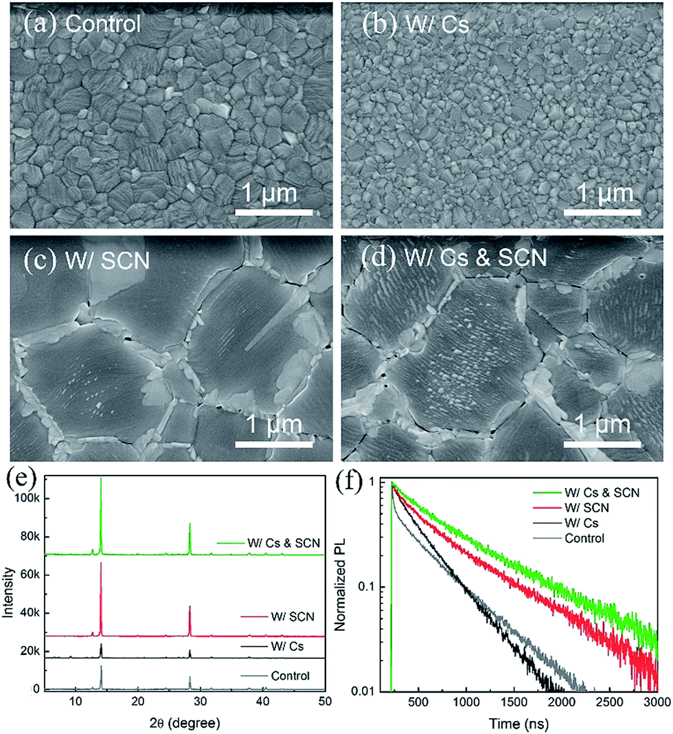 | ||
| Fig. 1 (a–d) SEM images, (e) XRD patterns and (f) TRPL decay of MA0.7FA0.3PbI3 films without and with Cs and/or SCN. | ||
Fig. 1(e) compares the X-ray diffraction (XRD) spectra of MA0.7FA0.3PbI3 films without and with Cs and/or SCN. The addition of Cs decreased the intensities of the perovskite (110) and (220) peaks compared to the control sample and introduced the δ-phase CsPbI3 impurities, as evident in the peaks at low 2θ angles of 9.8° and 13°.45 In contrast, adding Pb(SCN)2 additive to both the control and W/Cs films substantially enhanced the intensities of the perovskite peaks, indicating an increased degree of crystallinity, consistent with the SEM observation. Interestingly, the W/Cs & SCN sample shows no evidence of the δ-phase CsPbI3 impurities but a minor PbI2 peak at 12.8°. TRPL results reveal carrier lifetimes of 480, 360, 645 and 720 ns for samples of control, W/Cs, W/SCN, and W/Cs & SCN, respectively (Fig. 1(f)). It is worth noting that the MA0.7FA0.3PbI3 control sample exhibits a bi-exponential decay feature, likely related to the large density of grain boundaries because of the small grain size. Synergistic incorporation of Cs and SCN increased the grain size, improved the crystallinity and suppressed non-radiative recombination, leading to the longest carrier lifetime approaching 1 μs. A long carrier lifetime is critical to the performance of solar cells.14
We fabricated PVSCs in the n–i–p configuration to study the synergistic effects of Cs and SCN on the performance of PVSCs. The current density–voltage (J–V) curves and photovoltaic parameters of the corresponding devices are shown in Fig. 2(a) and Table S1,† respectively. Compared to the PCE of 17.16% for the MA0.7FA0.3PbI3 control device, the W/Cs device has a lower PCE of 16.22%. The reduced performance can mainly be ascribed to the deteriorated film quality with smaller grains, lower crystallinity, δ-CsPbI3 and impurity phase that led to a relatively shorter carrier lifetime than that of the control film. The W/SCN and W/Cs & SCN devices outperformed the control with PCEs of 18.83% and 19.92%, respectively, confirming the combined advantages of large crystal size and low trap density resulting from the Pb(SCN)2 additive.44
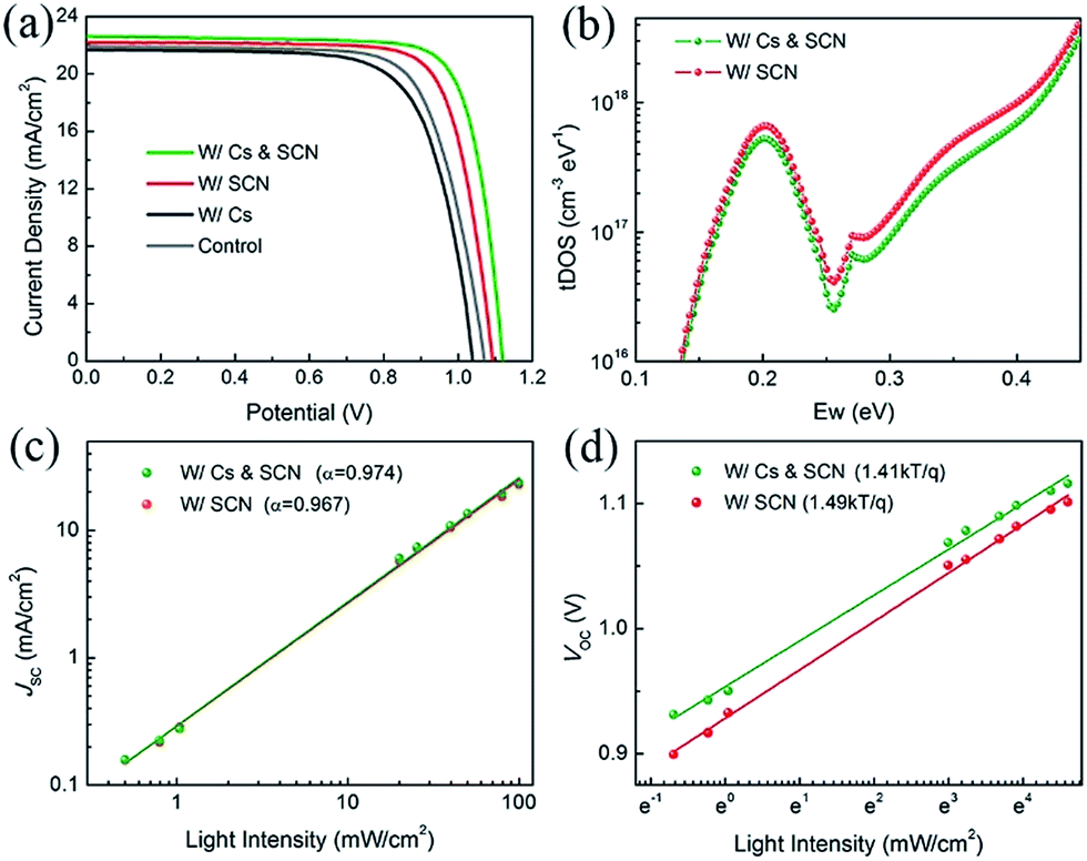 | ||
| Fig. 2 Characterization of the photovoltaic performance of the PVSCs. (a) J–V curves of PVSCs without and with Cs and/or SCN under reverse scan. (b) Trap density of states and light density dependence of (c) JSC and (d) VOC of W/SCN and W/Cs & SCN. | ||
To identify the reasons for the improved performance after incorporation of Cs and SCN, we employed additional characterization techniques to compare the two most efficient PVSCs with Pb(SCN)2. We first measured the trap density of states (tDOS) distribution of the devices using admittance spectroscopy. Fig. 2(b) shows that the W/Cs & SCN device has a lower trap density than the W/SCN one, which is consistent with lifetime measurements using TRPL. Further reduction of trap density is expected if the optimal Cs composition can be identified, as reported in the literature.46–48 We then investigated the light intensity dependence of JSC and VOC of PVSCs W/SCN and W/Cs & SCN. Fig. 2(c) shows the power law dependence of JSC on the light intensity on a double logarithmic scale. The fitted slopes (α) of the PVSCs with and without Cs are 0.974 and 0.967, respectively, indicating a slightly more balanced charge carrier transportation in the W/Cs & SCN device than in W/SCN.49 The VOC has a linear relationship with natural logarithmic light intensity, as shown in Fig. 2(d). The fitted slopes for the W/Cs & SCN and W/SCN devices are 1.41 and 1.49 kT/q, respectively, revealing a Shockley–Read–Hall recombination in both devices. However, the W/Cs & SCN device has a less steep slope, corresponding to a lower trap-assisted recombination than in the W/SCN device. The light dependence measurements indicate that the introduction of Cs and SCN will reduce the light-activated trap states. It was reported that the photocurrent degradation could be caused by the light-activated meta-stable deep-level trap states.48 The reduction of these defects would lead to better operational stability of PVSCs. The aforementioned results demonstrate the synergistic effects of Cs and SCN: SCN improves the film quality sufficiently, while Cs further reduces the light-activated trap density.47
To better understand the impact of Cs on the MA0.7FA0.3PbI3 with 2% Pb(SCN)2 films, we systematically investigated the properties of the films with different Cs fractions. We first characterized the optical properties of the (MA0.7FA0.3)1−xCsxPbI3 triple-cation perovskite thin films deposited on bare glass substrates using UV-visible spectroscopy. As shown in Fig. 3(a) and (b), the absorption onset and photoluminescence (PL) peak of the films show a slight blue shift after the introduction of Cs, indicating that the bandgap increases as the Cs content increases, consistent with reports by others.26 Tauc plots derived from absorbance spectra also show that the bandgap increases (Fig. S2†). Fig. S3† shows the photos of the Pb(SCN)2-incorporated (MA0.7FA0.3)1−xCsxPbI3 perovskite thin films deposited on glass substrates with different concentrations of Cs. When the Cs concentration exceeds 10%, the perovskite films become hazy, likely due to the formation of excessive CsPbI3 impurity phase.45 Fig. S4† shows the film-side reflectance spectra of these films; it is clear that the reflectance of perovskite films with the Cs concentration exceeding 15% is lower than that of the other films, confirming the smaller grain sizes and the existence of excessive CsPbI3 at the film surface.50 PL decays (Fig. 3(c)) indeed show that adding a small amount of Cs prolongs the carrier lifetime by reducing defects;47 however, adding a large amount Cs causes short lifetimes due to small grain size and poor crystallinity. The XRD patterns (Fig. S5†) show strong intensities of the (110) and (220) diffraction peaks at around 14.2° and 28.4°, respectively, indicating the similar preferred orientations for these films. The peak position of (110) shows a small shift to a higher angle after the introduction of CsPbI3 (Fig. S5(b)†), demonstrating the successful incorporation of Cs ions into the perovskite lattice since Cs has a smaller atomic radius compared to MA and FA.7 XRD patterns plotted on a log scale in the range from 5° to 20° (Fig. 3(d)) show the appearance of the orthorhombic CsPbI3 phase. Since the δ-phase CsPbI3 shows no desirable photovoltaic properties, the device performance will deteriorate when the amount of δ-phase CsPbI3 becomes very high.45 Hence, the amount of CsPbI3 in the precursor solution must be controlled to avoid the formation of significant amounts of δ-phase.46
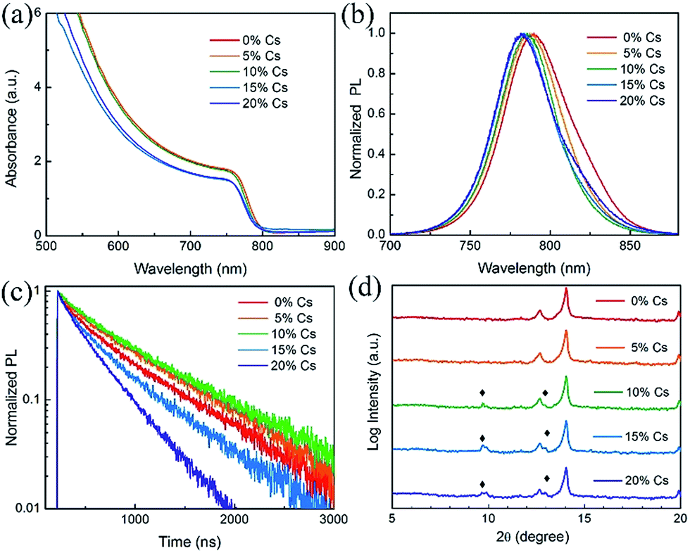 | ||
| Fig. 3 (a) Absorbance, (b) normalized PL, (c) PL decay and (d) XRD patterns of the Pb(SCN)2-incorporated (MA0.7FA0.3)1−xCsxPbI3 films with x varying from 0 to 20%. | ||
The SEM images show that the grain size has negligible change when the Cs content is lower than 10% (Fig. S6†); however, when the Cs concentration is above 15%, the grain size decreases dramatically, which is likely due to the acceleration of Cs ions in the nucleation process with more nuclei and consequent formation of small grains in the perovskite film.37 The SEM images also show that small brighter grains start to appear when the Cs concentration is higher than 10%. SEM-based X-ray energy dispersive spectroscopy (EDS) analysis indicated that these small brighter grains are CsPbI3. This is consistent with the XRD patterns shown in Fig. 3(d), which also reveal the formation of the CsPbI3 impurity phase when the concentration of Cs exceeds 10%. When the Cs concentration reached 15%, the grain size decreased dramatically, which means that the crystallinity decreases when a significant amount of δ-phase CsPbI3 starts to form. This is consistent with the XRD patterns shown in Fig. S5† in which the intensity of the (110) peak decreased and the FWHM increased when the Cs content exceeded 15%. Fig. S6(f)† shows the cross-sectional SEM image of a 10% Cs incorporated PVSC; the film has a very high aspect ratio and there are no lateral grain boundaries, making it desirable for charge transport.44,51
Fig. 4 shows the statistics of the photovoltaic parameters of 135 PVSCs measured under reverse voltage scans to confirm the effects of Cs on the device performance and reproducibility. The device performance of these PVSCs is summarized in Table S2.† The J–V and external quantum efficiency (EQE) curves of respective devices of the PVSCs with different Cs contents are shown in Fig. S7.† As the Cs concentration increases, the average VOC increases from 1.092 ± 0.003 (1.071 ± 0.013) V for the perovskite without Cs to 1.098 ± 0.008 (1.081 ± 0.010) V for that with 10% Cs measured under reverse (forward) voltage scan, due to the enhanced crystallinity as well as the increased bandgap.52 Any further increase in Cs concentration leads to decreased average VOC values, partially due to the formation of the CsPbI3 impurity phase. The average JSC also increases and reaches a maximum value of 22.82 ± 0.06 mA cm−2 at 10% Cs. This can only be explained by the improved crystallinity and film quality, since the bandgap increases as the Cs concentration increases. However, when the concentration of Cs is larger than 15%, the JSC decreases dramatically because of the formation of a large amount of CsPbI3 and the reduced grain size according to SEM. The trend of average FF as a function of Cs concentration can also be explained by the increased film quality and reduced traps at 10% Cs and then decreased grain size and crystallinity beyond 10% Cs.52 As a result, the average PCE increases from 19.47 ± 0.22 (17.86 ± 0.60)% for PVSCs without Cs to 19.98 ± 0.29 (18.63 ± 0.53)% for 10% Cs incorporated PVSCs measured under reverse (forward) voltage scans.
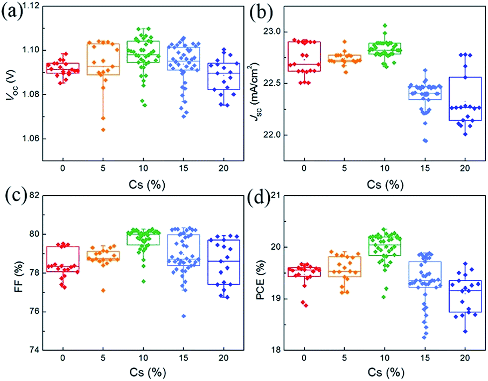 | ||
| Fig. 4 Statistical results of 135 PVSCs based on (MA0.7FA0.3)1−xCsxPbI3 perovskites with Cs content changing from 0 to 20%. | ||
Fig. 5 shows the photovoltaic performance of the best-performing PVSCs fabricated using a 10% Cs containing perovskite absorber. This device shows very small hysteresis when measured under reverse and forward voltage scans, as shown in Fig. 5(a). This PVSC exhibits a VOC of 1.11 (1.10) V, a JSC of 23.05 (23.05) mA cm−2 and a FF of 80.09 (79.69)%, yielding a PCE of 20.49 (20.21)%, when measured under reverse (forward) voltage scan at a sweep speed of 1 V s−1. Fig. 5(b) shows the EQE plot of the PVSC and the corresponding integrated current density of 22.56 mA cm−2, which is in good agreement with the JSC value obtained from the J–V curve. Due to the relatively small degree of hysteresis, our PVSCs show almost the same performance irrespective of scan speed, as shown in Fig. 5(c), maintaining a stable PCE of about 20.40% with negligible variation when measured under reverse voltage scan with different scan speeds. The best-performing PVSC shows a stable power output of 20.0% for 600 seconds using maximum power point tracking (MPPT) (Fig. 5(d)).
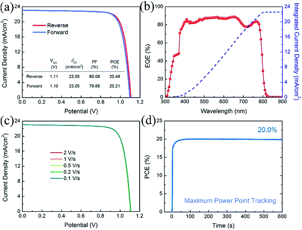 | ||
| Fig. 5 Photovoltaic parameters of the best-performing PVSCs with 10% Cs. (a) J–V curves measured under reverse and forward voltage scans with a scan rate of 1 V s−1. (b) The EQE plot and integrated current density curve. (c) J–V curves measured under reverse voltage scan with different scan speeds. (d) MPPT profile of the best-performing PVSC under 100 mW cm−2 AM 1.5G illumination. | ||
The introduction of Cs has been found to improve the long-term stability of PVSCs.7,26,53 However, some state-of-the-art Cs-containing PVSCs reported in the literature showed a certain degree of degradation under the initial illumination.25,26,29,54 To investigate the synergistic effects of Cs and SCN on the operational stability of PVSCs, especially under the initial illumination, we tracked the VOC and PCE of PVSCs without and with Cs and/or SCN, under 100 mW cm−2 AM 1.5G illumination. Fig. 6(a) shows the VOC profiles of the four PVSCs. The W/Cs & SCN device shows no change in VOC (1.12 V) after illumination for 3600 s. In contrast, the VOC of the W/SCN device decreased rapidly from its initial value of 1.10 V and plateaued at 1.05 V in the first 600 s. The W/Cs device also shows a stable VOC output; however, the value is inferior to that of the W/Cs & SCN device. Fig. 6(b) compares the MPPT profiles of PVSCs without and with Cs and/or Pb(SCN)2 under operating conditions in ambient air for 20000 s (∼6 h). Within the test group, the W/Cs & SCN device shows the highest PCE of 19.1% and the most stable power output, retaining 97% of its initial PCE after 20000 s of continuous operation under one sun illumination. This efficient and stable performance surpassed that of the control, W/Cs and W/SCN PVSCs measured under the same conditions, whose PCEs decreased to 71%, 91%, and 88% of their initial values, respectively, confirming the synergistic effects of SCN additive and Cs cations.
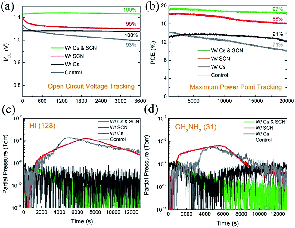 | ||
| Fig. 6 (a) Open-circuit voltage and (b) MPP tracking of VOC of PVSCs without encapsulation under 100 mW cm−2 AM 1.5G illumination in ambient air. Mass spectroscopy traces for (c) HI (m/z = 128) and (d) CH3NH2 (m/z = 31) released from the perovskite films during light induced decomposition measurements. | ||
To understand the origins of the operational stability of PVSCs with Cs incorporated perovskites, we performed mass spectroscopy measurements on the perovskite films with and without Cs. Fig. 6(c) and (d) show the traces of HI (m/z = 128) and CH3NH2 (m/z = 31) that were released from the MA0.7FA0.3PbI3-based perovskite films (control, W/Cs, W/SCN and W/Cs & SCN) under one sun illumination, respectively. The volatile HI and CH3NH2 gases are the main decomposition products of MAPbI3.29,55–57 The release of HI and CH3NH2 from the control and W/SCN samples indicates the photo-instability of the mixed MA/FA perovskites and could be the reason for the unstable performance of the corresponding devices under operating conditions, as shown in the MPPT measurements. The addition of Cs to the perovskite films effectively suppresses the photodegradation of the perovskite films (W/Cs and W/Cs & SCN), as evident from the substantial reduction of released of HI and CH3NH2 from the perovskite film under illumination. This could be the reason for the good operational stability of devices with both Cs and SCN.
Moreover, we checked the thermal stability of perovskite films by keeping them on a hotplate at different temperatures. As shown in Fig. S10,† the absorption onsets of perovskite films W/SCN and W/Cs & SCN are similar (around 800 nm); however, the absorbance of the W/Cs & SCN film shows a smaller change compared to that of the W/SCN one, indicating a better thermal stability. The moisture tolerance of perovskite films with and without Cs and/or SCN is shown in Fig. S11.† Among all the tested samples, the W/Cs film has the worst moisture tolerance probably due to the smallest grain size, making it vulnerable to moisture induced degradation. In contrast, simultaneous addition of Cs and SCN does not significantly change the stability of the films against moisture. Overall, the results show the synergistic effects of Cs and SCN on improving the quality and stability of perovskite films.
Conclusions
In conclusion, we have systematically investigated the synergistic effects of Cs and SCN additives on the performance and operational stability of PVSCs. The combination of Pb(SCN)2 and CsPbI3 results in high quality perovskite films with large grain sizes, high crystallinity, reduced trap density, and improved photostability, consequently leading to high performance PVSCs that can sustain a high power output with negligible degradation during continuous operation for 20000 seconds under AM 1.5G illumination.
Experimental
Precursor preparation
PbI2 (Alfa Aesar, 99.9985%), MAI (Dyesol), FAI (Dyesol), lead thiocyanate (Pb(SCN)2 (Sigma-Aldrich, 99.5%)), DMSO (Sigma-Aldrich, 99.8%), and DMF (Sigma-Aldrich, 99.8%) were purchased and used directly. Based on reports in the literature, we choose compositions of Csx(MA0.7FA0.3)1−xPbI3 for our study owing to the suitable bandgap of the MA0.7FA0.3PbI3 perovskite absorber for terrestrial solar cell applications (1.57 eV).41,58 We first made individual MA0.7FA0.3PbI3 and CsPbI3 precursors by dissolving mixed FAI, MAI, PbI2 and Pb(SCN)2 powders and mixed CsI, PbI2 and Pb(SCN)2 powders in mixed N,N-dimethylformamide (DMF) and dimethyl sulfoxide (DMSO) solvents, respectively, and then mixed these precursors in the desirable volume ratios to form (MA0.7FA0.3PbI3)1−x(CsPbI3)x precursors (Fig. S1†). The solutions were stirred overnight on a 60 °C hotplate before deposition. The amount of Pb(SCN)2 in perovskite precursors is 2.0% with respect to PbI2.Fabrication of solar cells
Our PVSCs have the regular cell configuration glass/FTO/PEALD SnO2/C60-SAM/(MA0.7FA0.3PbI3)1−x(CsPbI3)x/spiro-OMeTAD/Au. Here, FTO stands for fluorine-doped tin oxide (SnO2:F), C60-SAM stands for self-assembled fullerene monolayer, PEALD SnO2 is the electron selective layer (ESL) deposited by plasma-enhanced atomic layer deposition43 and spiro-OMeTAD is the 2,2′,7,7′-tetrakis(N,N′-di-p-methoxyphenylamine)-9,9′-spirobifluorene hole selective layer (HSL).20,59 The perovskite precursor solution was spin-coated on the ESL first at 500 rpm for 3 s, and then at 4000 rpm for 60 s with diethyl ether as the anti-solvent agent dropped on the film at 10 s of the second step. The as-prepared perovskite film was annealed on a hotplate at 65 °C for 2 minutes and then at 100 °C for 5 minutes. The typical thickness of our perovskite layers is about 500 nm. The spiro-OMeTAD solution was prepared following a procedure reported previously by us.39–41,44 All of the fabrication processes were conducted in a N2 filled glovebox.Characterization
Scanning electron microscopy (SEM) images were taken with a Hitachi S-4800 high resolution microscope. XRD patterns were acquired with a Rigaku Ultima III high resolution X-ray diffractometer using the Cu-Kα line (λ = 0.15481 nm) at 44 kV with 40 mA source excitation. Absorbance spectra were characterized with a UV-visible spectrophotometer (PerkinElmer Lambda 1050). J–V curves were measured using a Keithley 2400 sourcemeter, with the samples under AM 1.5G (100 mW cm−2) illumination (PV Measurements Inc.), the voltage of which was scanned between −0.1 V and 1.3 V. EQE spectra were measured using a commercialized QE system (PV Measurements Inc.). All device characterizations were performed in ambient air (∼22 °C, 30% humidity). A 532 nm continuous-wave laser at 40 mW cm−2 was used as an excitation wavelength for steady-state photoluminescence (PL) measurements, and the PL signal was detected by a Symphony-II CCD (from Horiba) detector through a 300 g mm−1 grating monochromator. Time resolved photoluminescence (TRPL) measurements were performed with a time correlated single photon counting module and the radiative recombination events were detected by a hybrid APD/PMT module (R10467U-50). Mass spectroscopy measurements were performed using an in-house-built temperature programmed desorption system.Conflicts of interest
The authors declare no competing financial interest.Acknowledgements
This work is financially supported by the U.S. Department of Energy (DOE) SunShot Initiative under the Next Generation Photovoltaics 3 program (DE-FOA-0000990), the Office of Naval Research under Contract no. N00014-17-1-2223, Air Force Research Laboratory, Space Vehicles Directorate (contract # FA9453-11-C-0253), National Science Foundation under contract no. CHE-1230246 and DMR-1534686, and the Ohio Research Scholar Program. This work also received financial support from the National Basic Research Program of China (2011CB933300), National Science Fund for Distinguished Young Scholars (50125309), and National Natural Science Foundation of China (Grants 51272184 and 91433203).Notes and references
- A. Kojima, K. Teshima, Y. Shirai and T. Miyasaka, J. Am. Chem. Soc., 2009, 131, 6050–6051 CrossRef PubMed.
- M. M. Lee, J. Teuscher, T. Miyasaka, T. N. Murakami and H. J. Snaith, Science, 2012, 338, 643–647 CrossRef PubMed.
- M. Liu, M. B. Johnston and H. J. Snaith, Nature, 2013, 501, 395–398 CrossRef PubMed.
- D. P. McMeekin, G. Sadoughi, W. Rehman, G. E. Eperon, M. Saliba, M. T. Hörantner, A. Haghighirad, N. Sakai, L. Korte, B. Rech, M. B. Johnston, L. M. Herz and H. J. Snaith, Science, 2016, 351, 151–155 CrossRef PubMed.
- N. J. Jeon, J. H. Noh, W. S. Yang, Y. C. Kim, S. Ryu, J. Seo and S. I. Seok, Nature, 2015, 517, 476–480 CrossRef PubMed.
- W. S. Yang, J. H. Noh, N. J. Jeon, Y. C. Kim, S. Ryu, J. Seo and S. I. Seok, Science, 2015, 348, 1234–1237 CrossRef PubMed.
- M. Saliba, T. Matsui, K. Domanski, J.-Y. Seo, A. Ummadisingu, S. M. Zakeeruddin, J.-P. Correa-Baena, W. R. Tress, A. Abate, A. Hagfeldt and M. Grätzel, Science, 2016, 354, 206–209 CrossRef PubMed.
- W. S. Yang, B.-W. Park, E. H. Jung, N. J. Jeon, Y. C. Kim, D. U. Lee, S. S. Shin, J. Seo, E. K. Kim, J. H. Noh and S. I. Seok, Science, 2017, 356, 1376–1379 CrossRef PubMed.
- D. Bi, W. Tress, M. I. Dar, P. Gao, J. Luo, C. Renevier, K. Schenk, A. Abate, F. Giordano and J.-P. C. Baena, Sci. Adv., 2016, 2, e1501170 Search PubMed.
- A. Mei, X. Li, L. Liu, Z. Ku, T. Liu, Y. Rong, M. Xu, M. Hu, J. Chen and Y. Yang, Science, 2014, 345, 295–298 CrossRef PubMed.
- W. Liao, D. Zhao, Y. Yu, C. R. Grice, C. Wang, A. J. Cimaroli, P. Schulz, W. Meng, K. Zhu, R.-G. Xiong and Y. Yan, Adv. Mater., 2016, 28, 9333–9340 CrossRef PubMed.
- W. Liao, D. Zhao, Y. Yu, N. Shrestha, K. Ghimire, C. R. Grice, C. Wang, Y. Xiao, A. J. Cimaroli, R. J. Ellingson, N. J. Podraza, K. Zhu, R.-G. Xiong and Y. Yan, J. Am. Chem. Soc., 2016, 138, 12360–12363 CrossRef PubMed.
- Z. Yu, B. Chen, P. Liu, C. Wang, C. Bu, N. Cheng, S. Bai, Y. Yan and X. Zhao, Adv. Funct. Mater., 2016, 26, 4866–4873 CrossRef.
- D. Zhao, Y. Yu, C. Wang, W. Liao, N. Shrestha, C. R. Grice, A. J. Cimaroli, L. Guan, R. J. Ellingson, K. Zhu, X. Zhao, R.-G. Xiong and Y. Yan, Nat. Energy, 2017, 2, 17018 CrossRef.
- M. Yang, Z. Li, M. O. Reese, O. G. Reid, D. H. Kim, S. Siol, T. R. Klein, Y. Yan, J. J. Berry, M. F. A. M. van Hest and K. Zhu, Nat. Energy, 2017, 2, 17038 CrossRef.
- W. Ke, C. Xiao, C. Wang, B. Saparov, H.-S. Duan, D. Zhao, Z. Xiao, P. Schulz, S. P. Harvey, W. Liao, W. Meng, Y. Yu, A. J. Cimaroli, C.-S. Jiang, K. Zhu, M. Al-Jassim, G. Fang, D. B. Mitzi and Y. Yan, Adv. Mater., 2016, 28, 5214–5221 CrossRef PubMed.
- D. Zhao, W. Ke, C. R. Grice, A. J. Cimaroli, X. Tan, M. Yang, R. W. Collins, H. Zhang, K. Zhu and Y. Yan, Nano Energy, 2016, 19, 88–97 CrossRef.
- Y. Yu, D. Zhao, C. R. Grice, W. Meng, C. Wang, W. Liao, A. J. Cimaroli, H. Zhang, K. Zhu and Y. Yan, RSC Adv., 2016, 6, 90248–90254 RSC.
- W. Ke, D. Zhao, C. R. Grice, A. J. Cimaroli, J. Ge, H. Tao, H. Lei, G. Fang and Y. Yan, J. Mater. Chem. A, 2015, 3, 17971–17976 RSC.
- Z. Song, A. Abate, S. C. Watthage, G. K. Liyanage, A. B. Phillips, U. Steiner, M. Graetzel and M. J. Heben, Adv. Energy Mater., 2016, 6, 1600846 CrossRef.
- Z. Song, C. L. McElvany, A. B. Phillips, I. Celik, P. W. Krantz, S. C. Watthage, G. K. Liyanage, D. Apul and M. J. Heben, Energy Environ. Sci., 2017, 10, 1297–1305 RSC.
- D. Bryant, N. Aristidou, S. Pont, I. Sanchez-Molina, T. Chotchunangatchaval, S. Wheeler, J. R. Durrant and S. A. Haque, Energy Environ. Sci., 2016, 9, 1655–1660 RSC.
- N. Aristidou, I. Sanchez-Molina, T. Chotchuangchutchaval, M. Brown, L. Martinez, T. Rath and S. A. Haque, Angew. Chem., Int. Ed., 2015, 54, 8208–8212 CrossRef PubMed.
- Q. Wang, B. Chen, Y. Liu, Y. Deng, Y. Bai, Q. Dong and J. Huang, Energy Environ. Sci., 2017, 10, 516–522 RSC.
- K. Domanski, E. A. Alharbi, A. Hagfeldt, M. Grätzel and W. Tress, Nat. Energy, 2018, 3, 61–67 CrossRef.
- M. Saliba, T. Matsui, J.-Y. Seo, K. Domanski, J.-P. Correa-Baena, M. K. Nazeeruddin, S. M. Zakeeruddin, W. Tress, A. Abate, A. Hagfeldt and M. Gratzel, Energy Environ. Sci., 2016, 9, 1989–1997 RSC.
- J. Liang, C. Wang, Y. Wang, Z. Xu, Z. Lu, Y. Ma, H. Zhu, Y. Hu, C. Xiao, X. Yi, G. Zhu, H. Lv, L. Ma, T. Chen, Z. Tie, Z. Jin and J. Liu, J. Am. Chem. Soc., 2016, 138, 15829–15832 CrossRef PubMed.
- Z. Li, M. Yang, J.-S. Park, S.-H. Wei, J. J. Berry and K. Zhu, Chem. Mater., 2016, 28, 284–292 CrossRef.
- J.-W. Lee, D.-H. Kim, H.-S. Kim, S.-W. Seo, S. M. Cho and N.-G. Park, Adv. Energy Mater., 2015, 5, 1501310 CrossRef.
- H. Choi, J. Jeong, H.-B. Kim, S. Kim, B. Walker, G.-H. Kim and J. Y. Kim, Nano Energy, 2014, 7, 80–85 CrossRef.
- T. Duong, Y. Wu, H. Shen, J. Peng, X. Fu, D. Jacobs, E.-C. Wang, T. C. Kho, K. C. Fong, M. Stocks, E. Franklin, A. Blakers, N. Zin, K. McIntosh, W. Li, Y.-B. Cheng, T. P. White, K. Weber and K. Catchpole, Adv. Energy Mater., 2017, 7, 1700228 CrossRef.
- H. Tsai, R. Asadpour, J.-C. Blancon, C. C. Stoumpos, O. Durand, J. W. Strzalka, B. Chen, R. Verduzco, P. M. Ajayan, S. Tretiak, J. Even, M. A. Alam, M. G. Kanatzidis, W. Nie and A. D. Mohite, Science, 2018, 360, 67–70 CrossRef PubMed.
- Y. Yu, C. Wang, C. R. Grice, N. Shrestha, J. Chen, D. Zhao, W. Liao, A. J. Cimaroli, P. J. Roland, R. J. Ellingson and Y. Yan, ChemSusChem, 2016, 9, 3288–3297 CrossRef PubMed.
- L. Guan, X. Yin, D. Zhao, C. Wang, Q. An, J. Yu, N. Shrestha, C. R. Grice, R. A. Awni, Y. Yu, Z. Song, J. Zhou, W. Meng, F. Zhang, R. J. Ellingson, J. Wang, W. Tang and Y. Yan, J. Mater. Chem. A, 2017, 5, 23319–23327 RSC.
- K. Aitola, K. Domanski, J.-P. Correa-Baena, K. Sveinbjörnsson, M. Saliba, A. Abate, M. Grätzel, E. Kauppinen, E. M. J. Johansson, W. Tress, A. Hagfeldt and G. Boschloo, Adv. Mater., 2017, 29, 1606398 CrossRef PubMed.
- M. Salado, M. Oliva-Ramirez, S. Kazim, A. R. González-Elipe and S. Ahmad, Nano Energy, 2017, 35, 215–222 CrossRef.
- T. Bu, X. Liu, Y. Zhou, J. Yi, X. Huang, L. Luo, J. Xiao, Z. Ku, Y. Peng, F. Huang, Y.-B. Cheng and J. Zhong, Energy Environ. Sci., 2017, 10, 2509–2515 RSC.
- B. Philippe, M. Saliba, J.-P. Correa-Baena, U. B. Cappel, S.-H. Turren-Cruz, M. Grätzel, A. Hagfeldt and H. Rensmo, Chem. Mater., 2017, 29, 3589–3596 CrossRef.
- C. Wang, L. Guan, D. Zhao, Y. Yu, C. R. Grice, Z. Song, R. A. Awni, J. Chen, J. Wang, X. Zhao and Y. Yan, ACS Energy Lett., 2017, 2, 2118–2124 CrossRef.
- C. Wang, C. Xiao, Y. Yu, D. Zhao, R. A. Awni, C. R. Grice, K. Ghimire, I. Constantinou, W. Liao, A. J. Cimaroli, P. Liu, J. Chen, N. J. Podraza, C.-S. Jiang, M. M. Al-Jassim, X. Zhao and Y. Yan, Adv. Energy Mater., 2017, 7, 1700414 CrossRef.
- C. Wang, D. Zhao, Y. Yu, N. Shrestha, C. R. Grice, W. Liao, A. J. Cimaroli, J. Chen, R. J. Ellingson, X. Zhao and Y. Yan, Nano Energy, 2017, 35, 223–232 CrossRef.
- F. Liu, Q. Dong, M. K. Wong, A. B. Djurišić, A. Ng, Z. Ren, Q. Shen, C. Surya, W. K. Chan, J. Wang, A. M. C. Ng, C. Liao, H. Li, K. Shih, C. Wei, H. Su and J. Dai, Adv. Energy Mater., 2016, 6, 1502206 CrossRef.
- C. Wang, D. Zhao, C. R. Grice, W. Liao, Y. Yu, A. Cimaroli, N. Shrestha, P. J. Roland, J. Chen, Z. Yu, P. Liu, N. Cheng, R. J. Ellingson, X. Zhao and Y. Yan, J. Mater. Chem. A, 2016, 4, 12080–12087 RSC.
- Y. Yu, C. Wang, C. R. Grice, N. Shrestha, D. Zhao, W. Liao, L. Guan, R. A. Awni, W. Meng, A. J. Cimaroli, K. Zhu, R. J. Ellingson and Y. Yan, ACS Energy Lett., 2017, 2, 1177–1182 CrossRef.
- A. Swarnkar, A. R. Marshall, E. M. Sanehira, B. D. Chernomordik, D. T. Moore, J. A. Christians, T. Chakrabarti and J. M. Luther, Science, 2016, 354, 92–95 CrossRef PubMed.
- S. Tang, Y. Deng, X. Zheng, Y. Bai, Y. Fang, Q. Dong, H. Wei and J. Huang, Adv. Energy Mater., 2017, 7, 1700302 CrossRef.
- Y. Hu, E. M. Hutter, P. Rieder, I. Grill, J. Hanisch, M. F. Aygüler, A. G. Hufnagel, M. Handloser, T. Bein, A. Hartschuh, K. Tvingstedt, V. Dyakonov, A. Baumann, T. J. Savenije, M. L. Petrus and P. Docampo, Adv. Energy Mater., 2018, 1703057, DOI:10.1002/aenm.201703057.
- W. Nie, J. C. Blancon, A. J. Neukirch, K. Appavoo, H. Tsai, M. Chhowalla, M. A. Alam, M. Y. Sfeir, C. Katan, J. Even, S. Tretiak, J. J. Crochet, G. Gupta and A. D. Mohite, Nat. Commun., 2016, 7, 11574 CrossRef PubMed.
- V. Mihailetchi, J. Wildeman and P. Blom, Phys. Rev. Lett., 2005, 94, 126602 CrossRef PubMed.
- D.-Y. Son, J.-W. Lee, Y. J. Choi, I.-H. Jang, S. Lee, P. J. Yoo, H. Shin, N. Ahn, M. Choi, D. Kim and N.-G. Park, Nat. Energy, 2016, 1, 16081 CrossRef.
- Z. Xiao, Q. Dong, C. Bi, Y. Shao, Y. Yuan and J. Huang, Adv. Mater., 2014, 26, 6503–6509 CrossRef PubMed.
- T. Singh and T. Miyasaka, Adv. Energy Mater., 2018, 8, 1700677 CrossRef.
- H. Tan, A. Jain, O. Voznyy, X. Lan, F. P. García de Arquer, J. Z. Fan, R. Quintero-Bermudez, M. Yuan, B. Zhang, Y. Zhao, F. Fan, P. Li, L. N. Quan, Y. Zhao, Z.-H. Lu, Z. Yang, S. Hoogland and E. H. Sargent, Science, 2017, 355, 722–726 CrossRef PubMed.
- J. Song, l. liu, X.-F. Wang, G. Chen, W. Tian and T. Miyasaka, J. Mater. Chem. A, 2017, 5, 13439–13447 RSC.
- S. Ito, S. Tanaka, K. Manabe and H. Nishino, J. Phys. Chem. C, 2014, 118, 16995–17000 CrossRef.
- S. Wang, Y. Jiang, E. J. Juarez-Perez, L. K. Ono and Y. Qi, Nat. Energy, 2016, 2, 16195 CrossRef.
- D. B. Mitzi and K. Liang, J. Solid State Chem., 1997, 134, 376–381 CrossRef.
- Z. Yang, C.-C. Chueh, P.-W. Liang, M. Crump, F. Lin, Z. Zhu and A. K. Y. Jen, Nano Energy, 2016, 22, 328–337 CrossRef.
- Z. Yu and L. Sun, Adv. Energy Mater., 2015, 5, 1500213 CrossRef.
Footnotes |
| † Electronic supplementary information (ESI) available. See DOI: 10.1039/c8se00200b |
| ‡ These authors contributed equally to this work. |
| This journal is © The Royal Society of Chemistry 2018 |