
 Open Access Article
 This Open Access Article is licensed under a
 Creative Commons Attribution 3.0 Unported Licence
Recent advances in flexible memristors for advanced computing and sensing
Jiaming
Xu
,
Ziwang
Luo
,
Long
Chen
,
Xuhui
Zhou
,
Haozhe
Zhang
,
Yuanjin
Zheng
* and
Lei
Wei
 *
*
School of Electrical and Electronic Engineering, Nanyang Technological University, 50 Nanyang Avenue, 639798, Singapore, Singapore. E-mail: yjzheng@ntu.edu.sg; wei.lei@ntu.edu.sg
First published on 26th June 2024
Abstract
Conventional computing systems based on von Neumann architecture face challenges such as high power consumption and limited data processing capability. Improving device performance via scaling guided by Moore's Law becomes increasingly difficult. Emerging memristors can provide a promising solution for achieving high-performance computing systems with low power consumption. In particular, the development of flexible memristors is an important topic for wearable electronics, which can lead to intelligent systems in daily life with high computing capacity and efficiency. Here, recent advances in flexible memristors are reviewed, from operating mechanisms and typical materials to representative applications. Potential directions and challenges for future study in this area are also discussed.
 Jiaming Xu | Jiaming Xu is pursuing his PhD degree at Nanyang Technological University in Singapore, affiliated with the Centre of Optical Fibre Technology at the School of Electrical and Electronic Engineering, under the supervision of Prof. Lei Wei. He received the BE degree in Materials Science and Engineering from Harbin Institute of Technology in 2020, and the MSc degree in Materials Science and Engineering from National University of Singapore in 2022. His research interests are fiber-based sensors and computing devices. |
 Yuanjin Zheng | Yuanjin Zheng is a professor at Nanyang Technological University in Singapore. He received his PhD degree from Nanyang Technological University in 2001. He joined Nanyang Technological University as an assistant professor in 2009. He also serves as the Director of the Centre for Integrated Circuits and Systems. His current research includes GHz RFIC and SoC, biomedical imaging, radar and UWB systems and circuits, SAW/acoustic/MEMS sensors, and energy and power conversion circuits. |
 Lei Wei | Lei Wei is an associate professor at Nanyang Technological University in Singapore. He received the PhD degree from Technical University of Denmark in 2011. He joined Nanyang Technological University in 2014 and was promoted to associate professor with tenure in 2019. He serves as the Director of the Centre of Optical Fibre Technology. He is also the chairman of the IEEE Photonics Society Singapore Chapter and the chair of the Optica (formerly OSA) Singapore Section. His main research interests are fiber-based devices, multifunctional fibers, bio-fiber interfaces, and in-fiber energy generation and storage. |
Wider impactConventional computing systems based on the von Neumann architecture face challenges such as high power consumption and limited data processing capability. Emerging memristors can provide a promising solution to achieve high-performance computing systems with ultra-low power consumption based on “in-memory computing”. The study of flexible memristors is an important topic and can bring new possibilities for wearable electronics. This paper systematically discusses the mechanisms, materials, fabrication techniques, and applications of flexible memristors that have been developed in recent years. We believe future studies in this area will focus on both material fabrication and device integration. For example, more nano-structured materials will be explored to provide better device performance. The study of low-temperature fabrication techniques will be essential to achieve enhanced compatibility with flexible substrates. As flexible memristors can be easily integrated with various wearable electronic components, a wide range of smart systems with self-learning and self-adaptation capabilities remain to be developed for signal processing, wearable electronics, robotics, and human-computer interfaces. This review provides a clear insight regarding the current challenges, potential solutions, and future perspectives, guiding the study of this highly exciting field. |
1. Introduction
The development of artificial intelligence and the Internet of Things (IoT) brings the requirement for increasing computing capacity. Conventional computing systems are currently facing challenges of energy efficiency and the von Neumann bottleneck.1–3 As a result, von Neumann architecture is no longer considered a promising choice for future computing systems, mainly due to the separation of processing and memory units, which hinders the improvement of data processing speed and leads to high power consumption.4–6 Besides, the trend of increasing computing capacity by device scaling is hard to continue considering the intensive cost and physical limitations, which is regarded as the major challenge of Moore's Law. The emerging memristive devices can provide a promising solution for massive data processing with high energy efficiency, based on the concept of performing data storage and processing within the same unit, called “in-memory computing”.4,7,8 The basic element of such devices is called a memristor, and this concept was first described by L. Chua in 1971.9 He inferred that there should exist the fourth fundamental passive circuit element besides the resistor, capacitor, and inductor that links electric charge and magnetic flux linkage, which he called the memristor. The function of a memristor cannot be duplicated with any combination of resistors, capacitors, and inductors. The memristor has a pinched hysteresis effect, and its resistance state depends on the past voltage or current. The first physical demonstration of memristors was reported by HP labs in 2008, based on a metal/insulator/metal structure.10 Since then, various mechanisms, structures, and materials have been developed for memristors. Although the argument exists whether memristors have been realized so far,11–13 it is generally considered that a memristor is a non-linear two-terminal memory device with switchable resistance.14,15 A memristor usually consists of two electrodes and a functional layer between them for memory, forming a sandwich structure. The resistance of the functional layer can be switched via multiple mechanisms, so the memory effect can be tuned. A memristor typically exhibits two discrete stable resistance states, and the switching between the low-resistance state (LRS) and the high-resistance state (HRS) is controlled by the input signal. Such memristors are often referred to as resistive random-access memories (ReRAM) or digital type memristors. Recently, memristors with multiple discrete resistance states have been developed to provide more freedom for multi-bit storage and computing.16–19 There also exist analog type memristors with continuously tunable resistance states, which are very similar to biological synapses with tunable synaptic weight, bringing new possibilities to advanced computing systems.20–23 Many encouraging functions can be realized by mimicking biological synapses with memristors. Considering the high stability, low power consumption, and promising application, the study of memristors and integrated neural networks has become increasingly significant in recent years.24–28Nowadays, most electronic devices are based on rigid silicon substrates that can provide high performance but poor mechanical flexibility, limiting their applications. Properties such as conformability, stretchability, and bendability are necessary for wearable electronics, artificial e-skin, soft robotics, implantable devices, and more.29,30 The past few decades have witnessed the rapid development of wearable electronics in various aspects, including medical devices, healthcare systems, robotics, and human–machine interfaces. Compared to conventional rigid devices, wearable electronics can achieve the same functionalities more conveniently and have enhanced the interaction between the human body and devices, leading to a wider range of applications. Given the fast-growing IoT and fifth-generation (5G) technology, wearable electronics are expected to have ultra-fast data transmission rates, real-time processing capability, and high reliability. Despite the advances in functional materials and packaging designs, wearable electronics still face the challenges of achieving high computing capacity, high data transmission rate, and low power consumption. This is mainly due to the limitations of CMOS technologies and constrained power supply devices. With the continuous growth of the IoT, the generated large volume of data sets a higher requirement for the capacity and efficiency of computing networks. A common solution is to transmit sensor data to external servers for processing, which still cannot reduce the total energy consumption and induces additional problems of transmission and propagation delay. Thus, a paradigm named “edge computing” has been introduced, which brings computing and memory units close to the data source for higher computing efficiency.31–33 Real-time pre-processing of the generated data is conducted by the edge computing system, and only the most important information is transmitted to the cloud server. As a promising candidate for wearable electronics, flexible memristors can enable this paradigm, taking advantage of their power efficiency, scalability, and adaptability.
Here, we review the recent progress in the development of flexible memristors for advanced sensing and computing systems. First, we summarize the typical mechanisms and materials for flexible memristors. Then, application examples for advanced computing and sensing systems are presented along with the device structures. Finally, we discuss the potential directions and challenges for future study in this area.
2. Mechanisms and materials
Integration of flexible memristors is mainly implemented by forming crossbar arrays on various flexible substrates. The top and bottom electrodes cross each other perpendicularly with the functional layer between them. Each intersection node is a memristor unit. The top and bottom electrodes of flexible memristors are usually made of Ag, Cu, Ni, Pt, Au, and TiN. Besides, indium tin oxide (ITO) can also be fabricated on flexible substrates as electrodes, especially for devices that require optical transparency. Materials for the functional layer differentiate from each other according to different operating mechanisms, as detailed below.2.1. Resistance switching mechanisms
As shown in Fig. 1, the resistance switching mechanisms of flexible memristors are the same as those of conventional memristors and can be classified into five categories: conductive filament, ion migration, charge trapping, ferroelectricity, and phase transition. The resistance switching of a flexible memristor is mostly triggered by the electrical signal, and a few examples of light-motivated memristors have also been reported,34–37 which enable potential applications in optical and optoelectronic computing and sensing systems. The mechanisms, materials, and device performance of recently developed flexible memristors are summarized in Table 1.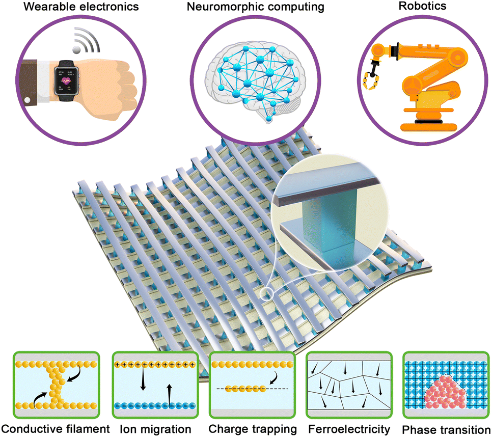 | ||
| Fig. 1 Applications and mechanisms of flexible memristors. | ||
| Mechanism | Substrate | Electrode | Functional layer | On/off resistance ratio | Switching voltage [V] | Retention time | Endurance [cycles] | Bending radius [mm] | Bending cycles | Ref. |
|---|---|---|---|---|---|---|---|---|---|---|
| Conductive filament | PET | Ag/Pt | PEI–AgClO4 | 103 | 1.2/−1.2 | 103 s | 500 | 5 | 200 | 38 |
| Conductive filament | PEN | Ag/ITO | Mn–ZnO | 2.7 × 10³ | 0.7/−0.6 | 104 s | 50 | 10 | 39 | |
| Conductive filament | PEN | Au/ITO | PMMA electrolyte | 104 | 6/−6 | 2.5 × 10³ s | 400 | 5 | 2500 | 40 |
| Conductive filament | Mica | Au/ITO | Cs2AgBiBr6 perovskite | >10 | 1.53/−3.4 | 105 s | 1000 | 9.25 | 104 | 41 |
| Conductive filament | PET | Au/ITO | MASnBr3 perovskite | 10–103 | 0.65/−3.5 | 104 s | 104 | 7.84 | 1000 | 42 |
| Conductive filament | Mica | Al-doped ZnO | NiO | >105 | 0.5/−0.5 | 105 s | 1000 | 6.5 | 1000 | 43 |
| Ion migration | Ag | Ag2S | 50–70 | 0.2/−0.2 | 104 s | 105 | 3 | 1000 | 44 | |
| Ion migration | PET | ITO | PEI/PAA electrolyte | 50 | 2.5/−1.5 | 104 s | 2 × 10⁴ | 2 | 104 | 45 |
| Charge trapping | PVP | Ag nanowires | Citric acid quantum dots | 105 | 2.5/0 | 104 s | 15 | 100 | 46 | |
| Charge trapping | PET | Au/ITO | Cs3Bi2I9 nanosheets | 103 | 0.3/−0.5 | 104 s | 1000 | 9 | 100 | 47 |
| Charge trapping | PEN | Al/ITO | InP/ZnSe/ZnS quantum dots | 8.5 × 10³ | 2.1/−3.1 | 104 s | 100 | 10 | 100 | 48 |
| Ferroelectricity | Mica | Au/SrRuO3 | BiFeO3 | >10 | 13/−16 | 5 | 104 | 49 | ||
| Ferroelectricity | PET | Au/Pt | BaTiO3/La0.7Sr0.3MnO3 | 5 | 3/−4 | 7 h | 1.5 | 100 | 50 | |
| Ferroelectricity | Mica | W/TiN | Hf0.5Zr0.5O2 | 20 | 3/−3 | 10 | 100 | 51 | ||
| Phase transition | PI | Pt/TiN | Sb2Te3/GeTe superlattice | 100 | 3.5/−3.5 | 104 s | 104 | 4 | 200 | 52 |
Most of the reported flexible memristors are digital type with binary resistance states, which is easily achievable for all the five mechanisms, and they are especially suitable for data storage and Boolean computing. Recently, multilevel and analog type flexible memristors with multiple or continuous tunable resistance states have also been reported, showing good application potential for neuromorphic computing systems.22,39,53 Unipolar and bipolar switching are the two switching behaviors found in memristors. The unipolar switching process is typically driven by thermal effects and the movement of ions or vacancies, which are independent of the voltage polarity. Unipolar memristors are often used in applications where a simple binary switching mechanism is sufficient, such as data storage and binary computing. For bipolar memristors, resistance switching depends on the polarity of the applied voltage. A positive voltage might switch the device to LRS, while a negative voltage might switch it back to HRS, or vice versa. The bipolar switching process is driven by mechanisms that are sensitive to the direction of the electric field. Bipolar memristors are often used in applications that require more complex switching behaviors, such as neuromorphic computing and programmable logic devices. Both unipolar and bipolar memristors can be analog type, but bipolar memristors are more commonly applied due to better control of resistance states.
Most filamentary memristors are digital type with abrupt resistance switching considering the process of forming conductive filaments. The generated filaments usually have good stability at room temperature, leading to relatively high device retention and durability. There are only a few reports on multilevel and analog type devices because it is hard to manipulate the growth and rupture of the filament.22,77 Moreover, the stochastic formation of conductive filaments can affect the uniformity and stability of the device, which is the main problem that remains to be addressed.
Ferroelectric memristors have better performance than filament based memristors because electric polarization can be precisely controlled. It is noted that the change in the ferroelectric domain is always continuous so that multilevel and continuous resistance switching between LRS and HRS can be achieved. Moreover, they also have the advantages of high switching speed, low switching energy, and good integration scalability. Most ferroelectric materials are rigid and have poor ductility and bending ability, which is the first problem that needs to be addressed. The reported ferroelectric materials for flexible memristors include BiFeO3,49 BaTiO3,50 and Hf0.5Zr0.5O2.51 More flexible ferroelectric materials remain to be explored. In most cases, muscovite mica is used as the substrate material, because the processing temperature of the ferroelectric materials is above the decomposition temperature of the commonly used polymer substrates. Recent studies have introduced a strategy that can prepare ferroelectric materials on a wide range of flexible substrates including polymers.86–88 In this case, ferroelectric thin film is first synthesized on a sacrificial buffer layer. After that, the buffer layer is removed so that the obtained ferroelectric film can be lifted off and attached to the target substrate.
One challenge for such memristors is that most phase change materials are difficult to fabricate on flexible substrates due to the uneven surface.89 The high temperature required for the fabrication and phase change process of such materials also impedes their applications in wearable electronics. As temperature plays an important role in the phase transition process, thermal management becomes an important topic, especially for device scaling. Another inevitable problem is the resistance shift caused by structural relaxation in the amorphous phase.90,91 This process is a thermally activated rearrangement of the amorphous structure at the atomic scale. The resistance increases spontaneously due to reduced concentration of point defects and localized states, as well as relaxation of compressive stress. Considering the above challenges, very few examples of flexible phase transition memristors have been reported so far. For example, Khan et al. prepared a phase-change memory device using a low-temperature fabricate technique.52 The superlattice phase-change material containing alternating Sb2Te3 and GeTe layers was directly sputtered on a flexible PI substrate at 180 °C. The flexible phase-change memory device exhibited multilevel resistance switching capability and ultralow reset current density. Moreover, van der Waals gaps in the superlattice material could help control structural relaxation and long-range atomic diffusion so that the resistance drift was suppressed and multilevel switching could be achieved. Another feasible fabrication method relies on the physical lift-off process.92,93 The phase change material is initially synthesized on a proper solid substrate and then transferred to the flexible substrate.
2.2. Flexible substrates
Substrates play an important role in achieving mechanical flexibility, user comfort, and other functionalities for wearable electronics. Flexible substrates serve as an intermediate layer between the human body and devices while protecting devices and interconnects from mechanical damage and environmental erosion. Many factors need to be considered for the selection of substrates including dielectric properties, thermal and chemical stability, surface roughness, interface adhesion, water resistance, permeability, and optical transparency. For wearable devices in direct contact with the human body, biocompatibility, non-toxicity, breathability, and comfortability are required for the long-term safety use of substrates. Moreover, the cost and scalability of substrates are critical for large-scale production and miniaturization of flexible electronics. Parameters of the commonly used flexible substrates and properties of different types of flexible substrates are summarized in Tables 2, 3 and Fig. 2.| Substrate | Glass transition temperature [°C] | Maximum service temperature [°C] | Thermal expansion coefficient [ppm °C−1] | Density [g cm−3] | Young's modulus [GPa] | Transparency |
|---|---|---|---|---|---|---|
| PET | 78 | 140 | 15–25 | 1.38 | 2.8 | Good |
| PEN | 120 | 155 | 18–20 | 1.36 | 3.0 | Good |
| PDMS | 125 | 350 | 310 | 0.96 | 2.1 | Good |
| PI | 340 | 400 | 50 | 1.36 | 2.6 | Poor |
| Mica | 500–600 | 9–36 | 2.82 | 1.4–2.1 | Poor | |
| PU | −35 | 90–150 | 15–210 | 0.05–1.7 | 0.02-5.5 | Poor |
| Substrate | Mechanical strength | Stretchability | Surface adhesion | Chemical stability | Thermal stability | Breathability |
|---|---|---|---|---|---|---|
| Polymers | Fair | Good | Fair | Fair | Poor–Fair | Poor–Fair |
| Mica | Good | Poor | Good | Good | Good | Poor |
| Hydrogels | Fair | Good | Fair–Good | Fair | Poor | Good |
| Porous polymers | Fair | Good | Fair | Fair | Poor–Fair | Good |
| Cellulose paper | Poor | Poor | Poor | Poor | Fair | Good |
| Fabrics | Good | Good | Poor–Fair | Fair–Good | Fair–Good | Good |
| Electrospun nanofibers | Good | Good | Good | Fair–Good | Fair–Good | Good |
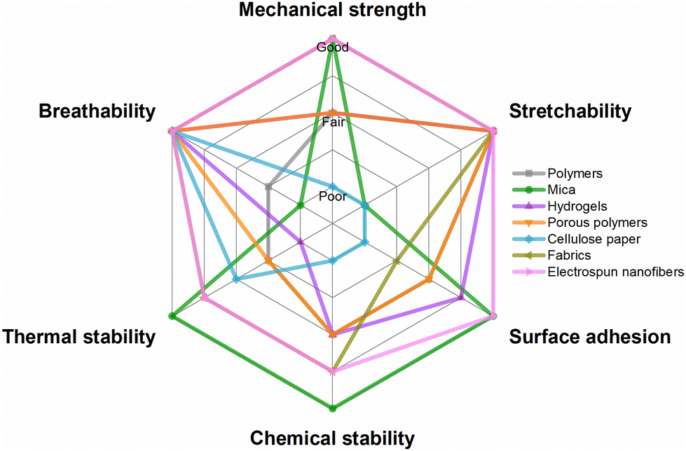 | ||
| Fig. 2 Properties of different types of flexible substrates. | ||
Generally, all substrates reported for wearable electronics can be potential candidates for flexible memristors. For most of the reported flexible memristors, the mechanical flexibility is attributed to polymer substrates. Polymeric substrates have the advantages of high mechanical flexibility, conformability, lightweight, and low cost, making them ideal for wearable applications. Polyethylene terephthalate (PET),38,54,94 polyethylene naphthalene (PEN),39,62,67 polydimethylsiloxane (PDMS),71,95,96 and polyimide (PI)52,97,98 are commonly used polymer substrates for flexible memristors. PET and PEN are both widely used electrical insulators with good stability, low gas permeability, low production cost, high strength, and relatively small thermal expansion coefficient. They provide good resistance to many solvents like ethanol, ketones, ester hydrocarbon, some acids, and certain alkalis. Also, their intrinsic transparency makes them suitable for optical applications. However, the relatively high stiffness limits their use for highly flexible applications.99 PDMS is a well-developed polymer substrate for flexible electronics. It has high mechanical flexibility and stretchability, good thermal and chemical stability, high transparency, and good biological compatibility. More importantly, mature technologies for surface modification of PDMS strongly enrich its functionalities, offering flexibility to tune its self-healing property, elasticity, modulus, and transparency.100 PI is another widely commercialized polymer substrate. It exhibits unique electrical properties, high mechanical strength, and high radiation and solvent resistance. Also, its high glass transition temperature and low thermal expansion coefficient can allow device fabrication with a processing temperature of up to 350 °C. However, the relatively high production cost, low solubility, and low transparency limit its applications.99,101 Although few demonstrations have been reported, copolymer elastomers, hydrogels, cellulose, and other organic materials also exhibit good potential to act as flexible substrates for memristors.102–104
Despite the low fabrication cost and good mechanical flexibility of these organic substrates, the low processing-stable temperature and poor adhesion are the major problems that affect the device's lifetime and stability. Recently, muscovite mica has been considered an ideal inorganic substrate for flexible electronics.105,106 The atomically flat surface and high thermal stability make it compatible with the fabrication of various materials. The absence of dangling bonds on the mica surface can mitigate the influence of lattice mismatch and thermal mismatch. Due to the weak van der Waals inter-layer interaction, the thickness of mica can be easily reduced via exfoliation to provide superior mechanical flexibility. The high mechanical strength and chemical inertness make it suitable for a wide range of application scenarios.
In many application scenarios, flexible devices need to be directly attached to the human body, which requires good breathability and lightweight. Therefore, substrates with high permeability like PDMS, PET, PI, and hydrogels are preferred in such cases. Besides, many porous materials exhibit good potential for flexible electronics considering their low density, large specific surface area, good deformability, high damage resistance, and enhanced chemical activity.107 There are two types of porous substrates based on different pore structures. Fiber-based porous substrates are woven textiles or fabrics composed of various fiber-based raw materials and usually have enhanced fatigue resistance. Non-fiber-based porous substrates are mostly porous elastomers with good stretchability such as porous PDMS and polyurethane (PU). Although the rough surface is not compatible with traditional CMOS processing technologies, a variety of methods have been demonstrated to construct electric components on porous substrates.108–111 Due to the large interfacial area and sufficient bonding sites, porous substrates can achieve enhanced interfacial adhesion. The porous structure also provides a large number of channels for air and water vapor, making the substrate breathable and comfortable for long-term wearing.
Recently, a new integration strategy has been introduced for flexible memristors without the use of flexible substrates.112–114 Herein, fiber-based memristors have been designed as woven textiles with intrinsic crossbar structures. Ag, Pt, and CNT fibers can be chosen as electrodes. Different functional layers can be directly fabricated on the fiber electrode surface via dip-coating or atomic layer deposition. Such design can help reduce the fabrication complexity and cost while offering good breathability and flexibility. The obtained textiles can be seamlessly integrated with other wearable electronics to achieve multi-functional smart textile systems.
2.3. Functional layers
The device performance of the memristor is directly related to the functional layer. The switching mechanism, functional materials, and layer thickness are three important factors that affect the resistance switching performance. It should be noted that although reducing the layer thickness and size within the proper range can help improve the device switching speed and lower the switching voltage, it can lead to reduced switching endurance, higher static power consumption, and larger device variation.34,115,116 Therefore, recent work on memristor performance is mainly focused on mechanism study and optimization of functional materials.3. Applications
Taking advantage of high flexibility and conformability, flexible electronics provide an imperceptible interaction between devices and the human body. The motion artifacts and mechanical mismatches can be effectively reduced compared with conventional rigid electronics, leading to better data quality.30 The development of flexible memristors also satisfies the requirement of achieving a higher level of comfort, convenience, connection, and intelligence for wearable devices in the era of artificial intelligence and IoT.140 The integration of flexible memristors and other flexible components is an ideal platform for designing multifunctional devices with excellent computing capability and energy efficiency, which can be widely used in smart textiles, healthcare equipment, soft robots, and human-machine interfaces.3.1. Advanced computing systems
Memristor logic circuits are fundamental building blocks for in-memory computing systems and can pave the way for studying advanced computing architectures. Input and output are stored in the memristor unit as the resistance state. The computing process is based on Boolean logic functions and requires arithmetic logic units. Therefore, digital type memristors with abrupt resistance switching are preferred. High on/off resistance ratio and long retention are important requirements for such non-volatile memory and binary computing. Fast switching speed and low switching voltage can help improve computing capability and efficiency. Recently, Jang et al. demonstrated NOT and NOR gates based on polymer memristor arrays (Fig. 3a and b).141 They also showed that other basic Boolean functions like OR, AND, and NAND gates could be implemented within the array by simply combining the NOT and NOR gates. Meng et al. introduced FALSE, material implication (IMP), and NAND logic gates using the flexible boron nitride-based memristors.53 The FALSE gate was achieved by applying the reset voltage to the memristor so that it always yielded logic “0”. The IMP gate contained two memristors and a series resistor (Fig. 3c). The input states were the initial resistance states of A and B, and the output state was the resistance state of B after applying voltage pulses. The NAND logic gate was realized by adding a parallel memristor (Device C) to the IMP gate circuit (Fig. 3d). The development of Boolean logic circuits based on flexible memristors provides the possibility for achieving digital in-memory computing systems with zero static power consumption and high efficiency.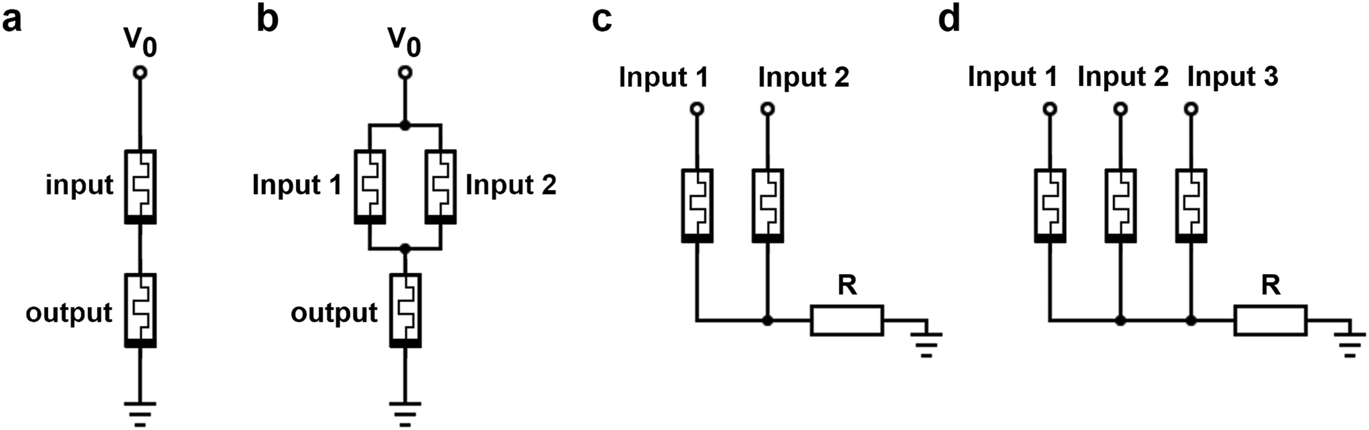 | ||
| Fig. 3 Schematic of the memristor-based (a) NOT gate, (b) NOR gate, (c) IMP gate, and (d) NAND gate. (a) and (b) Reproduced with permission.141 Copyright 2017, Springer Nature. (c) and (d) Reproduced with permission.53 Copyright 2021, Royal Society of Chemistry. | ||
Neuromorphic computing is a promising solution to go beyond von Neumann architecture and achieve massive data processing with low power consumption, inspired by the human brain structure. It has been widely used in data-intensive areas such as artificial intelligence (AI), IoT, and machine learning. The functions of a biological neural network are too complex to be artificially replicated. In a simplified model, a neural network is generally composed of two types of basic elements named neurons and synapses. All processing in neurons uses analog chemical signals. A neuron receives external input signals through dendrites and transmits them to other neurons through synapses. Synapse can scale the passing-through signals according to the synaptic weight so that learning capability can be achieved.2,142 Since neuromorphic computing systems require the ability to conduct memory and computation simultaneously, memristors are one ideal element for implementing such systems at the hardware level. The conductance of a memristor can represent synaptic weight and can be tuned by input signals. It should be noted that one type of three-terminal device named synaptic transistors is also under intensive study for neuromorphic computing systems. Compared with synaptic transistors, the two-terminal memristors have the advantages of low power consumption and compact device structure and can be easily integrated on a large scale.143 The simple two-terminal device can easily achieve high-density and large-scale integrated structures.
Memristor-based artificial synapses are regarded as a promising candidate for neuromorphic computing systems. The modulation of synaptic weights based on external stimuli is simulated by gradual resistance switching of the memristor. The change of resistance states of the memristor resembles synaptic plasticity, which describes the ability of synapses to strengthen or weaken the synaptic weight in response to stimuli. Therefore, multilevel and analog type memristors are always preferred for such applications. Large on/off resistance ratio, high linearity, good I–V symmetry, and low power consumption are important requirements for them. A sufficiently large resistance switching ratio can improve the identification accuracy of the resistance state and increase the dynamic range, offering better control of synaptic weight. Good linearity and I–V symmetry are both important to ensure uniform resistance change with the applied signal.
So far, many synaptic characteristics have been realized with memristors, including short-term plasticity (STP), short-term depression (STD), long-term plasticity (LTP), long-term depression (LTD), paired-pulse facilitation (PPF), spike-time-dependent plasticity (STDP), and spike-rating-dependent plasticity (SRDP).144–149 STP and STD are the temporal enhancement or decay of synaptic weight between the presynaptic neuron and the postsynaptic neuron within a short time scale of milliseconds to minutes, while LTP and LTD refer to the long-lasting change of synaptic weight. PPF is a form of STP characterized by an increase in sequentially evoked post-synaptic potentials. STDP describes the process that adjusts the synaptic connection strength depending on the relative timing of a particular neuron's input and output spikes. These characteristics are essential for the construction of neuromorphic computing systems.
Artificial neural networks (ANNs) and spiking neural networks (SNNs) are two commonly used machine learning models for neuromorphic computing systems. An ANN consists of connected nodes called artificial neurons. Each node connects to another and has the corresponding weight and threshold. The nodes are typically divided into an input layer, one or more hidden layers, and an output layer to perform different transformations on the input signal. If the output of any individual node is above a specified threshold, the node will be activated, sending a signal to the next layer. Nowadays, ANNs have been applied to a lot of areas like computer vision, natural language processing, and autonomous driving. Most existing ANNs are built on conventional computing systems with von Neumann architecture. For such software based ANNs, the learning parameters stored in memory are iteratively introduced to the processor to perform the task. The bottleneck issue arising from the movement of large datasets will eventually reduce energy and time efficiency when operating ANN software. Hardware-based ANNs composed of memristors can simultaneously transmit and process information without retrieving the stored parameters repeatedly. As a result, hardware-based ANNs are expected to address the bottleneck issue and provide much higher efficiency and computing capability.
Recently, Wang et al. introduced a flexible 3D ANN consisting of stacked crossbar Pt/HfAlOx/TaN memristor arrays for information transmission and processing.150 The fabricated memristor exhibited ultralow energy consumption down to 4.28 aJ per synaptic spike, even lower than a biological synapse. Multichannel information transmission was performed using a three-layer 6 × 6 crossbar memristor array. The tunable resistance of the memristors could simulate synaptic weight with continuous modulation for efficient neuromorphic computing. In this work, the 3D ANN with input layer (784 neurons), hidden layer (64 neurons), and output layer (10 neurons) was trained for MNIST pattern recognition, as shown in Fig. 4a, and the recognition accuracy was up to 88.8%. Besides, the ANN showed high fault tolerance as the recognition rate was higher than 80% and 70%, with the noise level of 30% and 60%, respectively (Fig. 4b and c). This work can inspire the development of neuromorphic computing systems with ultralow power consumption and high fault tolerance. Another good example reported recently is an in-sensor neuromorphic computing system based on flexible MXene-ZnO memristors.71 The memristors were integrated into an artificial visual system to preprocess the raw data, including noise suppression and filtering. Then, the information was transmitted to an ANN to complete the training of image recognition. The accuracy under different relative humidity ranges from 0% to 20% and 40% to 60% was 75.44% and 82.96%, respectively, indicating good environmental adaptability (Fig. 4d and e). This neuromorphic visual system could adapt to the environment with different light intensities and relative humidity while maintaining higher recognition accuracy compared to the system without the memristor arrays. This work provides a potential solution for multimodal in-sensor computing to reduce the circuitry complexity of traditional neuromorphic visual systems.
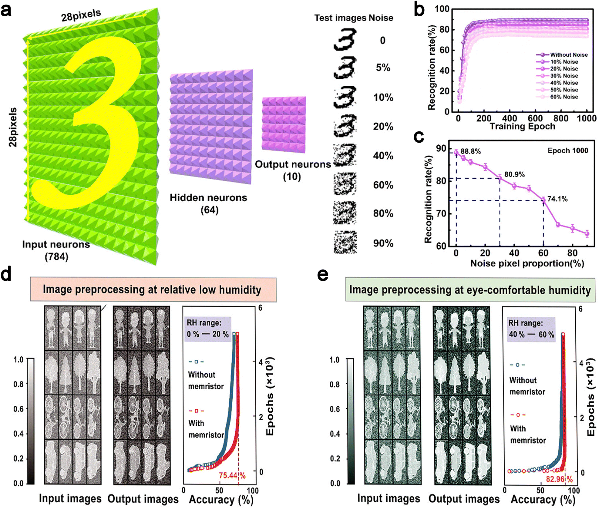 | ||
| Fig. 4 (a) Schematic of ANN in the MNIST pattern recognition process, consisting of the input layer (784 neurons), hidden layer (64 neurons), and output layer (10 neurons). The recognition rate as a function of (b) training epoch (0–1000) and (c) noise pixel proportion (0–90%). Recognition of the input image at a (d) low humidity condition and (e) eye-comfortable humidity condition on the contrast enhancement and denoising of the artificial retina sensing system. (a)–(c) Reproduced with permission.150 Copyright 2020, American Chemical Society. (d) and (e) Reproduced with permission.71 Copyright 2021, Wiley-VCH. | ||
A few modified types of ANNs have also been demonstrated on flexible memristor arrays recently, showing promising potential for applications like image recognition and combinatorial optimization. Zhang et al. developed a polymer memristor array that acted as both an in-memory Boolean logic element and a hardware accelerator for neuromorphic computing (Fig. 5a and b).151 The 2D conjugated polymer memristor is digital type with binary resistance states. A binary neural network (BNN) was built to perform pattern recognition. Herein, logic 0 and 1 are defined in accordance with HRS and LRS, while synaptic weights and neuron activations are set to be +1 or −1. Compared to most ANNs built with analog type memristors, the BNN can achieve more precise weight updating and better computing accuracy. The bit-wise operation can significantly reduce memory and computing resource usage. Simulation of offline supervised learning was conducted and achieved 99.23% recognizing accuracy for 10![[thin space (1/6-em)]](https://www.rsc.org/images/entities/char_2009.gif) 000 images (28 × 28 pixels) from the MNIST handwritten database. Online learning simulation also achieved a high recognizing rate of 97.13% after 1 epoch training with 60000 images. Kim et al. reported an example of using flexible memristors for combinatorial optimization of the max-cut problem (Fig. 5c and d).152 The Hopfield neural network (HNN) composed of a 6 × 6 memristor synapse array was developed to solve the max-cut problem with six nodes. The system consumed only about 75.3 fJ to get the solution, which is highly superior to other systems. The HNN also exhibited good potential for dealing with more complex combinatorial optimization, and a benchmark of the max-cut problem comprising large graphs was used for the analysis. This work offers a promising strategy for designing flexible neural networks with the ability to solve nonpolynomial hard problems, which is essential for the combination of wearable electronics and artificial intelligence systems.
000 images (28 × 28 pixels) from the MNIST handwritten database. Online learning simulation also achieved a high recognizing rate of 97.13% after 1 epoch training with 60000 images. Kim et al. reported an example of using flexible memristors for combinatorial optimization of the max-cut problem (Fig. 5c and d).152 The Hopfield neural network (HNN) composed of a 6 × 6 memristor synapse array was developed to solve the max-cut problem with six nodes. The system consumed only about 75.3 fJ to get the solution, which is highly superior to other systems. The HNN also exhibited good potential for dealing with more complex combinatorial optimization, and a benchmark of the max-cut problem comprising large graphs was used for the analysis. This work offers a promising strategy for designing flexible neural networks with the ability to solve nonpolynomial hard problems, which is essential for the combination of wearable electronics and artificial intelligence systems.
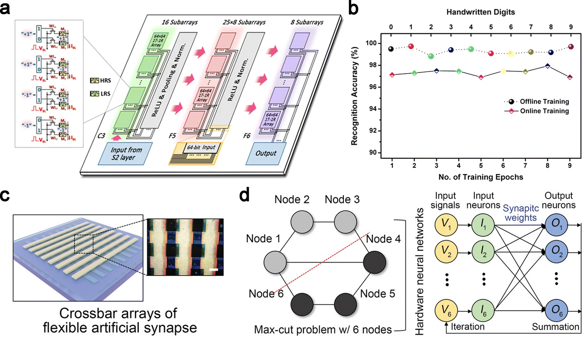 | ||
| Fig. 5 (a) Illustration of the PBDTT-BQTPA polymer memristor arrays in the binary neural network. (b) Recognition accuracies of the handwritten numeral images from the MNIST dataset through offline and online training. (c) A schematic of the crossbar arrays of the developed artificial synapse. The inset shows a microscopic image of the fabricated synapse arrays (scale bar, 500 μm). (d) Hopfield neural network developed for solving the max-cut problem composed of six nodes. (a) and (b) Reproduced with permission.151 Copyright 2021, Springer Nature. (c) and (d) Reproduced with permission.152 Copyright 2023, John Wiley and Sons. | ||
Compared with ANNs with static input, the operation of SNNs is based on dynamic spiking input as a function of time. When the membrane potential is beyond the threshold, the neuron generates a spike to postsynapses. Neurons in SNNs transmit information only when the membrane potential reaches the threshold. Therefore, SNNs can mimic biological neural networks more closely and have higher power efficiency. The most prominent spiking neuron model is the leaky integrate-and-fire model. The momentary activation level is considered as the neuron state. The incoming spikes make this value higher or lower until it reaches the threshold so that the neuron fires. After that, the neuron state returns to the reset state. Memristors with good scalability, low power consumption, and fast switching speed have been used to construct hardware-based SNNs. Among the synaptic characteristics mentioned before, STDP and SRDP are especially important for the construction of SNNs. The training process of SNNs depends on STDP or SRDP according to different signal encoding methods. The STDP learning rule illustrates the relationship between the timing of neurons and the updating of the weights. LTP occurs when postsynaptic spikes follow presynaptic spikes, and LTD occurs when postsynaptic spikes precede presynaptic spikes. The SRDP learning rule describes the synaptic weights modified by firing frequency. The high frequency of presynaptic spikes leads to LTP, and the low frequency induces LTD. Although the implementation of SNNs faces many challenges, like the lack of mature training algorithms and high computational complexity, several examples based on flexible memristors have been proposed with good application potential.
Tang et al. reported a flexible halide perovskite memristor and simulated the dynamics of the attributed artificial neuron.153 The artificial neuron model circuit was composed of a resistor as the synaptic weight, an output resistor for outputting spikes, and a capacitor for integrating charges (Fig. 6a). When the input voltage was applied, the capacitor began to charge along the R–C loop, and the membrane potential Vm increased (Fig. 6b). Once Vm reached the threshold, the memristor turned on, and the voltage applied on Rout increased drastically so that the artificial neuron generated a spike. Then, the capacitor began to discharge, leading to a decrease in Vm. During this process, the artificial neuron did not have any output response, which could emulate the refractory period of the biological neuron. Finally, the memristor was switched to HRS, and the artificial neuron returned to its original state. Wang et al. constructed a hardware SNN based on dual-mode memristor arrays.154 In this case, the resistance switching mode (RSM) and threshold switching mode (TSM) memristors were artificial synapses and output neurons, respectively. Unsupervised learning for digit recognition was successfully performed on this SNN consisting of 30 input neurons, 300 synapses, and 10 output neurons, suggesting its great potential for neuromorphic computing (Fig. 6c–g). However, it should be noted that since training with the SNN model remains a challenge, and the corresponding algorithms are more suitable for low-accuracy computing applications, ANNs are always preferred as the training model for neuromorphic computing systems, considering the faster speed and higher accuracy.
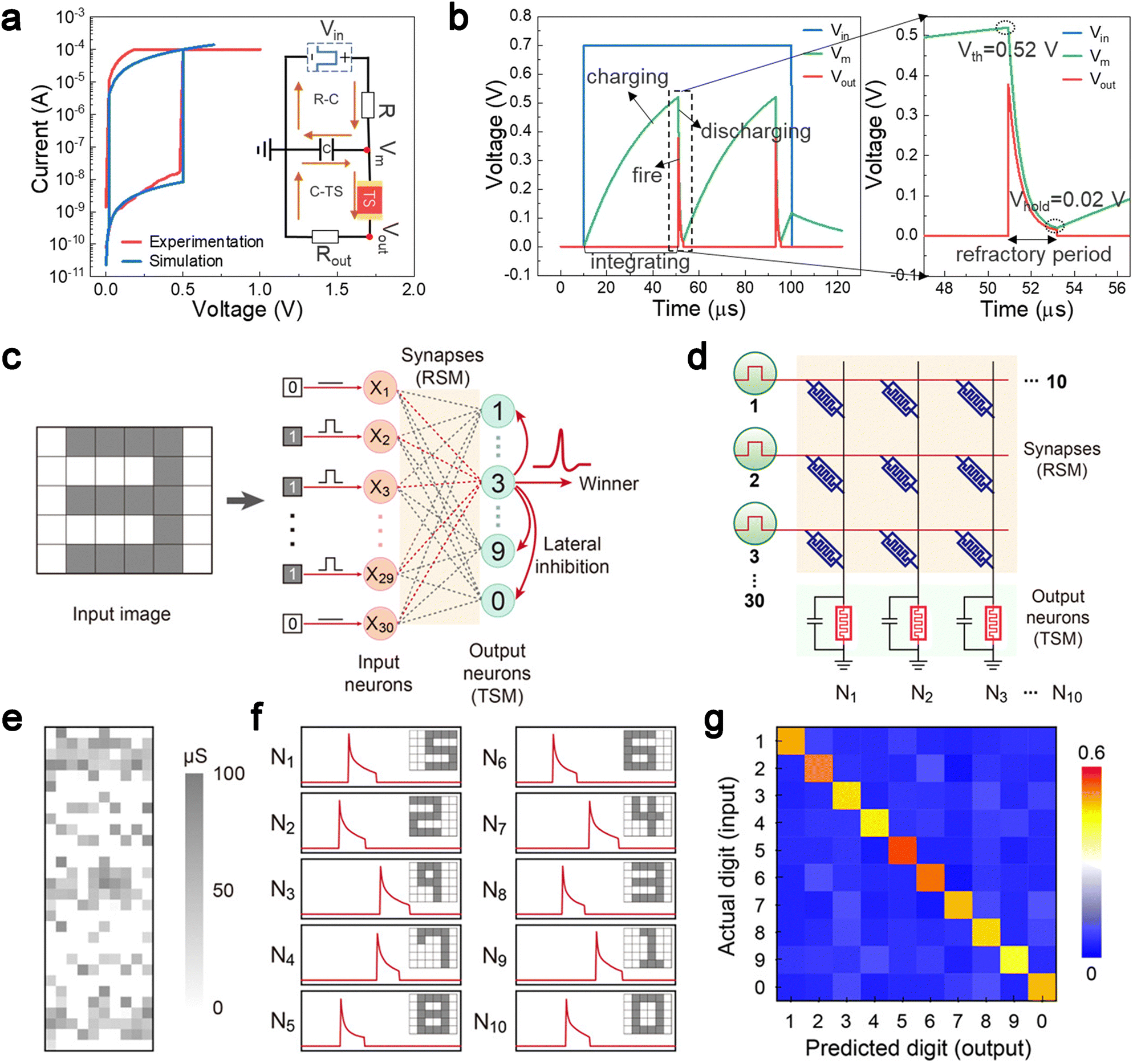 | ||
| Fig. 6 (a) Simulated I–V curve of the Au/OIHP/Au/PEN threshold switching memristor. The inset is a schematic diagram of the artificial neuron equivalent circuit. (b) Leaky integrate-and-fire dynamics of a threshold switching memristor-based artificial neuron. (c) Schematic of the two-layer SNN consisting of RSM synapses and TSM output neurons for digit recognition. (d) Illustration of the fully memristive SNN based on dual-mode memristor arrays in RS and TS modes for synapses and output neurons, respectively. (e) Conductance map of the RSM array after training. (f) Simulated output signals of the fired output neurons for the corresponding digits. N1–N10 represent the 10 output neurons as illustrated in (c). (g) Confusion matrix between actual (input) and predicted (output) digits. Large values along the diagonal line demonstrate the successful recognition of digits by the fully memristive SNN. (a) and (b) Reproduced with permission.153 Copyright 2022, Royal Society of Chemistry. (c)–(g) Reproduced with permission.154 Copyright 2022, John Wiley & Sons. | ||
3.2. Advanced sensing systems
Mechanical flexibility and stretchability make it possible to seamlessly integrate flexible memristors with varieties of sensors to achieve high-performance sensing systems for wearable electronics, healthcare systems, robotics, and human-machine interfaces. The biological nervous system exhibits various functions, including sensory perception, data integration process, motor command, physiologic function management, and cognitive processes (memory and learning). Biological nervous systems employ a decentralized, parallel, event-driven strategy, using synapses and neurons to process information. Considering the actual application scenario, artificial synapses based on memristors are basically for the preprocessing and computing of sensor signals. Synaptic characteristics introduced before are required depending on the data processing model. For example, humans fortify their tactile acuity through training and conditioning, furnishing them with immediate reactions to their ambiance. Therefore, STP and STD are important characteristics so that memristors can quickly process the signals from the sensors. In addition, using memory computing architectures in neuromorphic systems reduces the distance between the sensor and the processor. This promotes system compactness while enhancing energy efficiency.The development of flexible memristors can inspire the improvement of sensing capability and versatility for wearable electronics. Low energy consumption for wearable devices can be guaranteed by flexible memristors to achieve long battery life. The intrinsic crossbar structure and excellent computing capability of flexible memristors can inspire the development of smart textile electronics. For example, Liu et al. introduced a textile memristor array made of fiber electrodes with uniform CsPbBr3 quantum dot functional layers.112 The crossbar memristor structure was compatible with textile materials and could be integrated with other wearable electronics to enhance computing capacity. A real-time diagnosis tool for patients with arrhythmia diseases was demonstrated in this work (Fig. 7a–c). The memristor network could classify the collected electrocardiogram signal (ECG) patterns with a high accuracy of 83% after only 15 learning epochs. Another smart textile with a similar crossbar structure was demonstrated by Wang et al. based on Ag/MoS2/HfAlOx/carbon nanotube memristors.113 In this work, heating resistors were integrated with the memristor neural network to produce an intelligent heating textile (Fig. 7d–f). The frequency and heating time were regulated by the memristor-based artificial synapses and neurons, which were sensitive to the environment temperature and could be easily modulated.
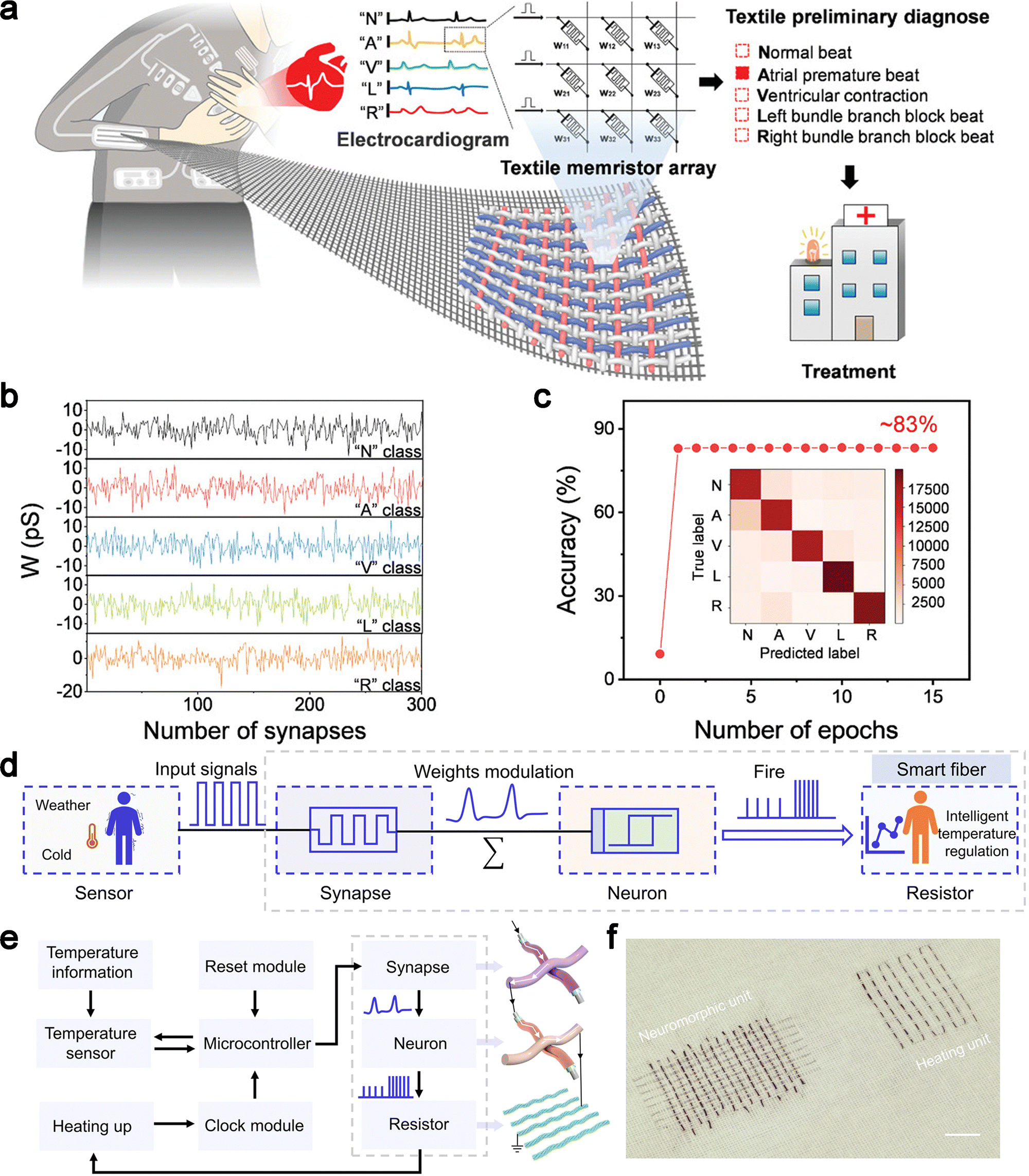 | ||
| Fig. 7 (a) Schematic of smart healthcare clothes integrated with textile memristor as information-processing components to analyze physiological information and display the categorizing results. (b) Featured weight values of each class connected to the output neuron after the learning process. (c) Recognition accuracy for ECG patterns corresponding to learning epochs and confusion matrix that compared predicted label with true label (inset). (d) Schematic of intelligent fiber heating system. (e) Operation mechanism of the intelligent warm fiber. (f) Photograph of the fiber-based intelligent heating memristors. Scale bar, 1 cm. (a)–(c) Reproduced with permission.112 Copyright 2022, Wiley-VCH. (d)–(f) Reproduced with permission.113 Copyright 2022, Springer Nature. | ||
Furthermore, by integrating flexible memristors with various sensors and other electronic components, advanced sensing and self-adaptive systems can be achieved to simulate human feelings, perceptions, and actions with very low power consumption. This can have a promising prospect in the areas of human–computer interfaces and humanoid robots. Nowadays, the simulation of human senses like touch, sight, and smell has all been realized.155–162 For example, Wang et al. developed a fast responsive artificial skin system that could simultaneously sense and process multiple tactile stimuli without conversion circuits (Fig. 8a–e).163 The artificial skin system consisted of a pressure sensor array for detecting tactile stimuli and a flexible memristor array for data processing. In this work, real-time detection of pressure patterns and near-sensor analog computing were conducted simultaneously, and the obtained result fitted well with the simulated one by software. Besides, the average power consumption of this artificial skin system could be 1000 times lower than a conventional interface electronic system, suggesting great application potential. Similarly, Jiang et al. introduced a bio-inspired electronic skin based on dual-excited pressure memory (DPM) matrix consisting of piezo-OLEDs and piezo-memristors (Fig. 8f–i).164 Resistance switching of the memristor can be triggered by both optical and potential signals. Real-time tactile imaging and memorizing were demonstrated on the DPM device with 15 × 15 units. The device shows a high on/off resistance ratio of about 810 and a stable storage of less than 4% resistance attenuation after 2 months.
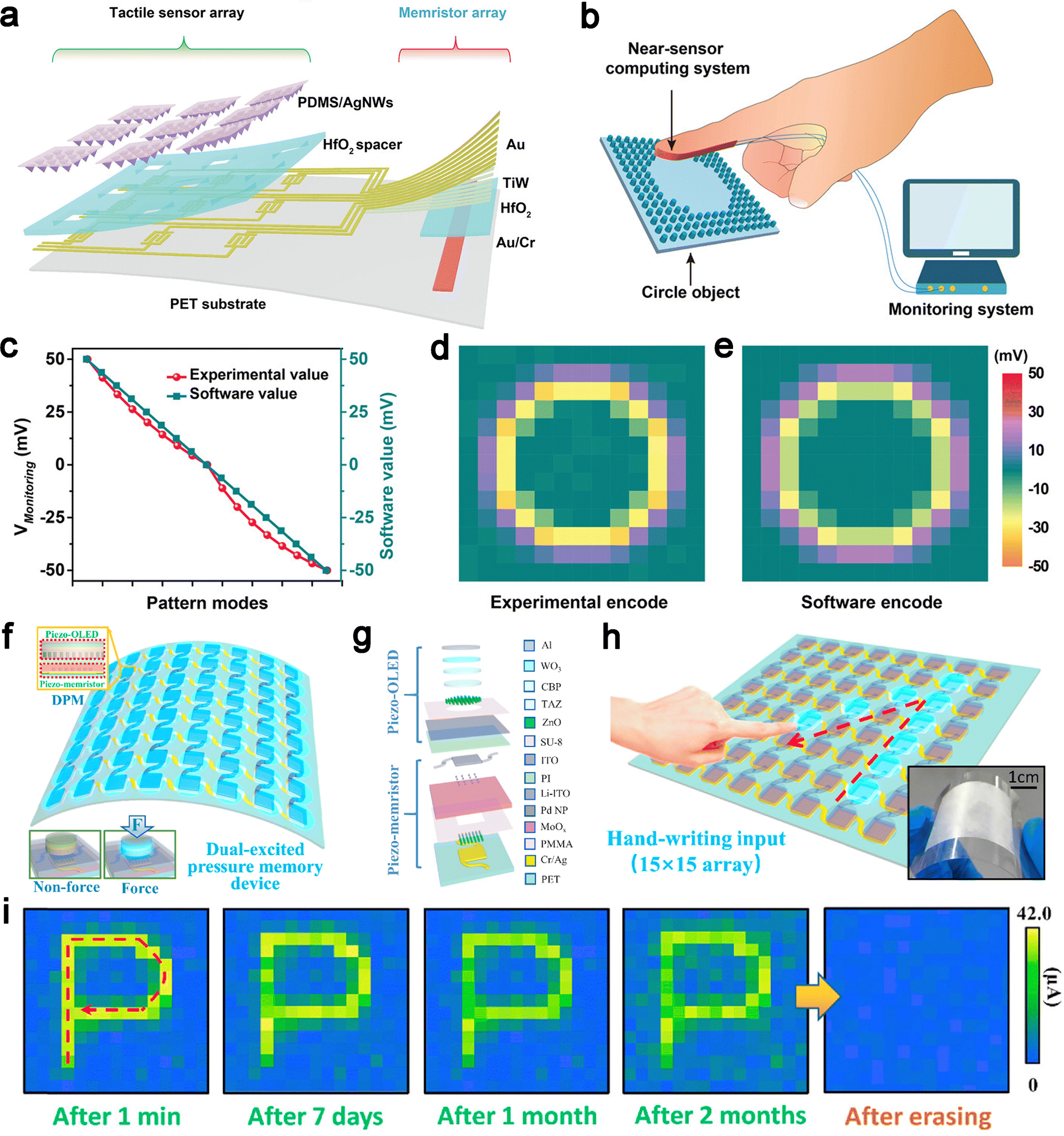 | ||
| Fig. 8 (a) Schematic of the near-sensor analog computing system experimentally implemented on a flexible substrate consisting of a 3 × 3 pyramidal pressure sensor array and a 9 × 1 memristor array. (b) Schematic of the experimental setup for edge detection. (c) Experimental VMonitoring was consistent with software-calculated values. Edge detection decoded from (d) the experiment and (e) software were nearly identical. (f) Configuration of the bio-inspired dual-excited pressure memory (DPM) device, combining with resistive-switching piezo-memristors and illumination-conversion piezo-OLEDs. (g) Detailed structure of the DPM device with the multi-stacked layers. (h) Schematic illustration of sensing and memorizing the data of pressure assignment from the handwriting. Inset is the photography of the fabricated DPM device with high flexibility. (i) Illustrations of the capabilities for the pressure memory with long-time storage and clear erasure by a letter “P” input. (a)–(e) Reproduced with permission.163 Copyright 2022, Wiley-VCH. (f)–(i) Reproduced with permission.164 Copyright 2020, Elsevier. | ||
For the artificial vision system, a biomimetic compound eye for real-time collision detection was reported recently, inspired by the structure of the lobula giant movement detector (LGMD) (Fig. 9a–e).165 It was composed of threshold-switching memristors based on few-layer black phosphorous nanosheets and CsPbBr3 perovskite quantum dots heterostructure (FLBP-CsPbBr3). The switching of the flexible memristor array was controlled by optical input via the temporal heat summation effect. The biomimetic compound eye exhibited wide field-of-view (FoV) detection capability and nonmonotonic collision avoidance response, which could be applied in autonomous robots for environment detection. Pei et al. introduced a high-speed artificial vision system capable of recognizing, memorizing, and actuating self-protection (Fig. 9f and g).166 It is composed of a Sb2Se3/CdS-core/shell nanorod array optoelectronic memristor, a threshold-switching memristor, and an electrochemical actuator. When an optoelectronic memristor is activated, it can cause an electrochemical actuator to move, simulating the eye muscle contraction and reproducing the self-protection response of closing eyes when the human eyes are injured by intense light. This system does not require complex signal processing circuits and can inspire the development of efficient robot vision systems.
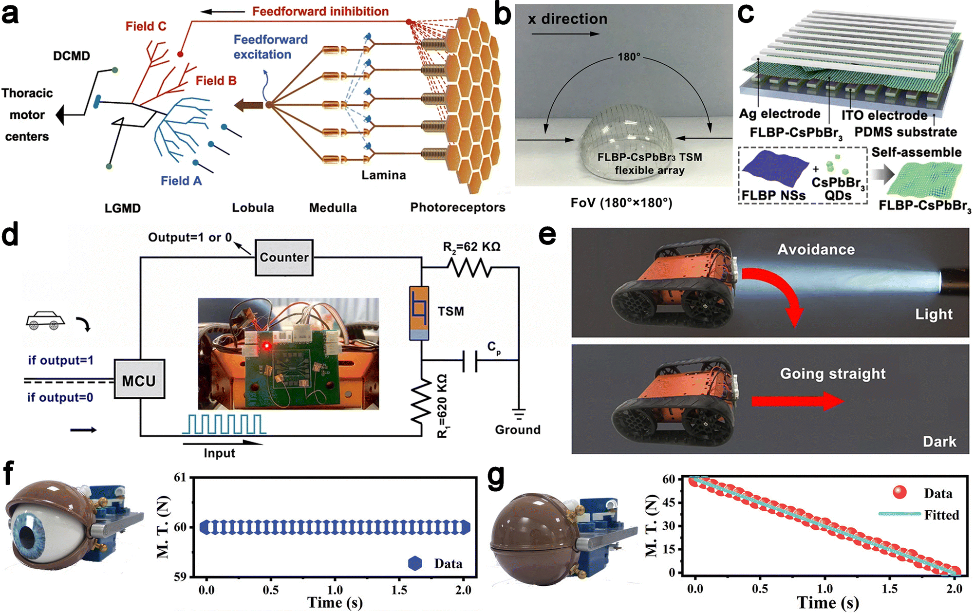 | ||
| Fig. 9 (a) Schematic of the anatomical organization of the vision system with LGMD. (b) Schematic of the device-level biomimetic compound eye. (c) Schematic diagram of the two-terminal threshold switching memristor (TSM) with the structure of Ag/few-layer black phosphorous nanosheets (NSs)-CsPbBr3 perovskite quantum dots (QDs) heterostructure (FLBP-CsPbBr3)/indium tin oxide (ITO). (d) Schematic illustration of the model car test setup. (e) Schematic decision-making for the robot car with optic signal processing ability. (f) The state of the eye muscles during contraction (eye opening) and the actuator pulling force value as a function of ordinary light exposure time. (g) The state of the eye muscles when they are relaxed (eyes closed) and the actuator pulling force value as a function of bright light exposure time. (a)–(e) Reproduced with permission.165 Copyright 2021, Springer Nature. (f)–(g) Reproduced with permission.166 Copyright 2022, Wiley-VCH. | ||
The reported work on simulation of the human sense of smell based on flexible memristors is relatively rare compared to those of artificial tactile and vision systems. Recently, Gao et al. introduced a flexible artificial olfactory system, which was the integration of Sr–ZnO-based gas sensors, HfOx-based memristors, and electrochemical actuators (Fig. 10a–d).167 The designed system realized olfactory functions without the need for tedious signal processing circuitry for data analysis and information storage. Ammonia detection and self-protection functions were also demonstrated in this work. When NH3 was detected by the gas sensor, the signal was processed and stored by the memristor. Meanwhile, activation of the memristor triggered the electrochemical actuator to block the gas flow channel for self-protection. By simply replacing the sensor part, the system could achieve the above functions for other gases and even odorless ones. Lu et al. developed a hybrid flexible gas sensory system with perceptual learning ability (Fig. 10e–h).160 It is a combination of a gas sensor, an oscillator as the artificial afferent nerve, and a memristor-type artificial synapse. The identification and recognition of H2S gas with various concentrations was demonstrated using a supervised learning method with the classic k-nearest neighbors (KNN) algorithm. A low error rate of about 20% was achieved after five times of training. This work can inspire the study of neuromorphic sensing systems with learning ability for robotics and human-machine interfaces.
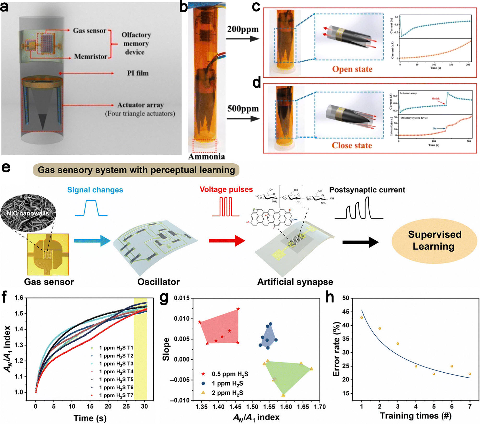 | ||
| Fig. 10 (a) Schematic illustration of the bionic nose (4 arc actuators in parallel). (b) The initial state of the bionic nose. (c) The photo and schematic diagram of the bionic nose's response to low concentration (200ppm) of ammonia, and the instantaneous current changes of the artificial olfactory system and actuator array. (d) The photo and schematic diagram of the bionic nose's response to high concentration (500ppm) of ammonia, and the instantaneous current changes of the artificial olfactory system and actuator array. (e) Schematic diagram of the hybrid flexible gas sensory system with perceptual learning. (f) Training dataset for the artificial system exposed to H2S ambient with a concentration of 1 ppm. (g) Boundaries after training for five times using the KNN algorithm. (h) The improvement in the recognition accuracy with the increased number of training times. (a)–(d) Reproduced with permission.167 Copyright 2021, Elsevier. (e)–(h) Reproduced with permission.160 Copyright 2021, Springer Nature. | ||
Another important topic in the areas of humanoid robots and artificial sensory systems is the study of artificial nociceptors (Fig. 11a). Humanoid robots can be helpful not only for daily life but also for dangerous tasks like disaster response and space exploration, where human operation is hard to realize. Artificial nociceptors can be an important part of such systems to protect them from hazards by sensing external noxious stimuli and generating warning signals.168–170 One of the most critical characteristics of a nociceptor is called “threshold”, which indicates that it only responds to the stimulus that exceeds a certain value. Besides, “no adaptation”, “relaxation”, “allodynia” and “hyperalgesia” are also notable characteristics that help protect the system from further damage. For example, no adaptation means that the intensity of the response does not change after prolonged exposure to the stimulus. Relaxation is related to the dissipation of the response to a stimulus. Allodynia is caused by a stimulus that normally causes no pain, while hyperalgesia refers to an increased sensitivity to the stimulus. Memristor-based artificial nociceptors can easily realize such functions with a simple device structure and low power consumption. Different stimuli like pressure and heating can be detected and processed based on the corresponding module connected to the memristor within the artificial nociceptor.94,117,171 The similar idea can also be applied to the design of artificial reflex arcs (Fig. 11b), a promising topic in the study of soft robotics.172,173 The integration of flexible memristors with multiple sensors and actuators can realize complex functions as artificial muscles for soft robots. Memristors generally act as the threshold controlling unit for such systems and can perform edge data processing to reduce system complexity and power consumption.
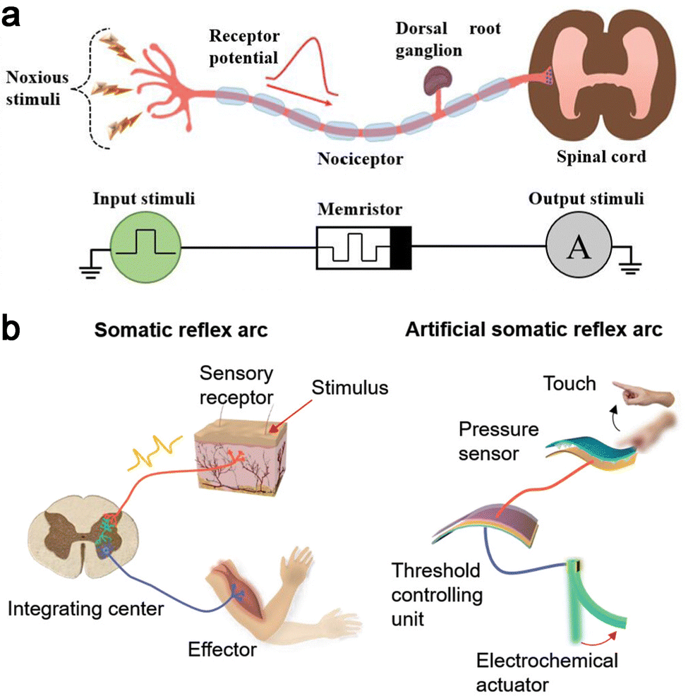 | ||
| Fig. 11 (a) Schematic illustration of biological nociceptor in the human body and an artificial nociceptor electrical circuit consisting of a threshold switching memristor. (b) Schematic comparison of the somatic reflex arc in human and artificial somatic reflex arc. (a) Reproduced with permission.171 Copyright 2023, American Chemical Society. (b) Reproduced with permission.173 Copyright 2019, Wiley-VCH. | ||
4. Summary and outlook
High power consumption and the von Neumann bottleneck are the main challenges for conventional computing systems. As we are about to reach the limit of Moore's Law, further improvement of device performance based on traditional CMOS technology cannot last long. The study of memristors has attracted intensive attention in recent years owing to the great application potential for next-generation computing systems with high performance and ultralow power consumption, which is very important for wearable electronics and portable devices that require high energy efficiency and compact size. Therefore, the development of flexible memristors has become an important topic. The operation mechanisms for flexible memristors are the same as traditional ones, and a wide range of materials have been developed. Conductive filament is the most commonly observed mechanism of flexible memristors, and sometimes it comes together with the charge trapping mechanism. Materials for such mechanisms can be easily fabricated using various low-temperature techniques and exhibit good compatibility with a wide range of flexible substrates. Therefore, these two mechanisms are the most maturely developed ones for flexible memristors. The main challenge is related to the stochastic formation of conductive filaments. Thus, the study of filament formation and control is necessary to reduce device variation. The non-filamentary ion migration mechanism provides a potential solution for this problem, but the related principles and material properties are not fully studied. This will be an important topic to be discussed further. Ferroelectricity and phase transition are two mature technologies for traditional non-volatile memory, which also have great potential for flexible memristors. Compared with the conductive filament mechanism, they can easily achieve good cycle-to-cycle and device-to-device uniformity while keeping the high switching speed and good device stability. They are seldom reported in recent years due to the challenges of material fabrication. The high fabrication temperature of ferroelectric and phase change materials can cause thermal deformation or even damage to certain flexible substrates. Besides, the uneven surface of many flexible substrates can lead to poor adhesion of the functional layers. Therefore, the following topics are critical for further study. One is to develop low-temperature and room-temperature fabrication technology for such materials. Another is to explore better high-temperature resistant materials like mica with low surface roughness and good mechanical flexibility. Other topics, such as improving the surface quality of flexible substrates and developing new materials and switching mechanisms, are also necessary. In recent years, 2D materials have exhibited good application potential for memristive devices. Based on their unique structure and properties, synaptic transistors with high stability and reliability have been demonstrated, showing better performance than conventional ones. The related work can inspire the development of 2D flexible memristors.Memristor logic circuits and memristor-based artificial neurons are fundamental components for in-memory computing and neuromorphic computing systems. Further advances in the study of device structures, system architectures, and algorithms can help reduce system complexity and improve computing efficiency. The study of device scaling and large-scale integration technologies is also necessary to improve the computing capacity and power efficiency. Device variation and parasitic resistance are the two main issues that need to be addressed for large-scale integration of memristors, which can be solved by material engineering and 3D integration. Various advanced systems for signal processing, wearable electronics, robotics, and human-computer interfaces can be achieved by integrating flexible memristors with other electronic components like sensors and actuators. These works are inspired by biological systems, and the proposed devices can conduct self-learning and self-adaptation to various external stimuli. More potential application scenarios and memristive system structures remain to be explored. Further study in this area can be inspired by potential breakthroughs in neuroscience so that related artificial systems can better mimic biological functions to achieve higher efficiency.
Author contributions
Jiaming Xu: writing – original draft, review & editing; Ziwang Luo: writing – review & editing; Long Chen: writing – review & editing; Xuhui Zhou: writing – review & editing; Haozhe Zhang: writing – review & editing; Yuanjin Zheng: supervision – supporting, writing – review & editing; Lei Wei: supervision – Lead, writing – review & editing.Data availability
No primary research results, software, or code have been included and no new data were generated or analyzed as part of this review.Conflicts of interest
There are no conflicts to declare.Acknowledgements
This work was supported by the Singapore Ministry of Education Academic Research Fund Tier 2 (MOE2019-T2-2-127, MOE-T2EP50120-0002 and MOE-T2EP50123-0014), the Singapore Ministry of Education Academic Research Fund Tier 1 (RG62/22), A*STAR under AME IRG (A2083c0062), A*STAR under IAF-ICP Programme I2001E0067 and the Schaeffler Hub for Advanced Research at NTU, the IDMxS (Institute for Digital Molecular Analytics and Science) by the Singapore Ministry of Education under the Research Centres of Excellence scheme, and the NTU-PSL Joint Lab collaboration.References
- J. Backus, Commun. ACM, 1978, 21, 613–641 CrossRef.
- J. Zhu, T. Zhang, Y. Yang and R. Huang, Appl. Phys. Rev., 2020, 7, 011312 CAS.
- J. Tang, F. Yuan, X. Shen, Z. Wang, M. Rao, Y. He, Y. Sun, X. Li, W. Zhang, Y. Li, B. Gao, H. Qian, G. Bi, S. Song, J. J. Yang and H. Wu, Adv. Mater., 2019, 31, 1902761 CrossRef CAS PubMed.
- M. A. Zidan, J. P. Strachan and W. D. Lu, Nat. Electron., 2018, 1, 22–29 CrossRef.
- N. K. Upadhyay, H. Jiang, Z. Wang, S. Asapu, Q. Xia and J. Joshua Yang, Adv. Mater. Technol., 2019, 4, 1800589 CrossRef.
- G. W. Burr, R. M. Shelby, A. Sebastian, S. Kim, S. Kim, S. Sidler, K. Virwani, M. Ishii, P. Narayanan, A. Fumarola, L. L. Sanches, I. Boybat, M. Le Gallo, K. Moon, J. Woo, H. Hwang and Y. Leblebici, Adv. Phys.: X, 2017, 2, 89–124 Search PubMed.
- D. Ielmini and H. S. P. Wong, Nat. Electron., 2018, 1, 333–343 CrossRef.
- G. Indiveri and S. C. Liu, Proc. IEEE, 2015, 103, 1379–1397 CAS.
- L. Chua, IEEE Trans. Circuit Theory, 1971, 18, 507–519 Search PubMed.
- D. B. Strukov, G. S. Snider, D. R. Stewart and R. S. Williams, Nature, 2008, 453, 80–83 CrossRef CAS PubMed.
- P. Meuffels and R. Soni, arXiv, 2012, preprint, arXiv:1207.7319 DOI:10.48550/arXiv.1207.7319.
- I. Abraham, Sci. Rep., 2018, 8, 10972 CrossRef PubMed.
- J. Kim, Y. V. Pershin, M. Yin, T. Datta and M. Di Ventra, Adv. Electron. Mater., 2020, 6, 2000010 CrossRef CAS.
- L. Chua, Appl. Phys. A: Mater. Sci. Process., 2011, 102, 765–783 CrossRef CAS.
- M. Lanza, A. Sebastian, W. D. Lu, M. Le Gallo, M. F. Chang, D. Akinwande, F. M. Puglisi, H. N. Alshareef, M. Liu and J. B. Roldan, Science, 2022, 376, eabj9979 CrossRef CAS PubMed.
- T. Y. Wang, J. L. Meng, L. Chen, H. Zhu, Q. Q. Sun, S. J. Ding, W. Z. Bao and D. W. Zhang, InfoMat, 2021, 3, 212–221 CrossRef.
- C. Wang, Z. Si, X. Jiang, A. Malik, Y. Pan, S. Stathopoulos, A. Serb, S. Wang, T. Prodromakis and C. Papavassiliou, IEEE J. Emerging Sel. Top. Circuits Syst., 2022, 12, 723–734 Search PubMed.
- G. Cao, C. Gao, J. Wang, J. Lan and X. Yan, Nano Res., 2022, 15, 8419–8427 CrossRef CAS.
- M. Ismail, H. Abbas, C. Choi and S. Kim, J. Alloys Compd., 2020, 835, 155256 CrossRef CAS.
- S. Kim, H. Kim, S. Hwang, M. H. Kim, Y. F. Chang and B. G. Park, ACS Appl. Mater. Interfaces, 2017, 9, 40420–40427 CrossRef CAS PubMed.
- J. Rao, Z. Fan, L. Hong, S. Cheng, Q. Huang, J. Zhao, X. Xiang, E. J. Guo, H. Guo, Z. Hou, Y. Chen, X. Lu, G. Zhou, X. Gao and J. M. Liu, Mater. Today Phys., 2021, 18, 100392 CrossRef CAS.
- B. C. Jang, S. Kim, S. Y. Yang, J. Park, J. H. Cha, J. Oh, J. Choi, S. G. Im, V. P. Dravid and S. Y. Choi, Nano Lett., 2019, 19, 839–849 CrossRef CAS PubMed.
- P. Zhang, M. Xia, F. Zhuge, Y. Zhou, Z. Wang, B. Dong, Y. Fu, K. Yang, Y. Li, Y. He, R. H. Scheicher and X. S. Miao, Nano Lett., 2019, 19, 4279–4286 CrossRef CAS PubMed.
- K. Sun, J. Chen and X. Yan, Adv. Funct. Mater., 2021, 31, 2006773 CrossRef CAS.
- Q. Zhao, Z. Xie, Y. P. Peng, K. Wang, H. Wang, X. Li, H. Wang, J. Chen, H. Zhang and X. Yan, Mater. Horiz., 2020, 7, 1495–1518 RSC.
- S. Kumar, X. Wang, J. P. Strachan, Y. Yang and W. D. Lu, Nat. Rev. Mater., 2022, 7, 575–591 CrossRef.
- R. Wang, J. Q. Yang, J. Y. Mao, Z. P. Wang, S. Wu, M. Zhou, T. Chen, Y. Zhou and S. T. Han, Adv. Intell. Syst., 2020, 2, 2000055 CrossRef.
- D. S. Jeong, K. M. Kim, S. Kim, B. J. Choi and C. S. Hwang, Adv. Electron. Mater., 2016, 2, 1600090 CrossRef.
- P. Wang, M. Hu, H. Wang, Z. Chen, Y. Feng, J. Wang, W. Ling and Y. Huang, Adv. Sci., 2020, 7, 2001116 CrossRef CAS PubMed.
- W. Gao, H. Ota, D. Kiriya, K. Takei and A. Javey, Acc. Chem. Res., 2019, 52, 523–533 CrossRef CAS PubMed.
- W. Shi, J. Cao, Q. Zhang, Y. Li and L. Xu, IEEE Internet Things J., 2016, 3, 637–646 Search PubMed.
- O. Krestinskaya, A. P. James and L. O. Chua, IEEE Trans. Neural Networks Learn. Syst., 2020, 31, 4–23 Search PubMed.
- B. Varghese, N. Wang, S. Barbhuiya, P. Kilpatrick and D. S. Nikolopoulos, 2016 IEEE International Conference on Smart Cloud (SmartCloud), 2016, DOI:10.1109/SmartCloud.2016.18.
- Y. Wang, F. Wu, X. Liu, J. Lin, J. Y. Chen, W. W. Wu, J. Wei, Y. Liu, Q. Liu and L. Liao, Appl. Phys. Lett., 2019, 115, 193503 CrossRef.
- S. Chen, Z. Lou, D. Chen and G. Shen, Adv. Mater., 2018, 30, 1705400 CrossRef PubMed.
- L. Chen, R. Li, S. Yuan, A. Chen, Y. Li, T. Zhang, L. Wei, Q. Zhang and Q. Li, Matter, 2023, 6, 925–939 CrossRef CAS.
- Y. Liu, L. Wu, Q. Liu, L. Liu, S. Ke, Z. Peng, T. Shi, X. Yuan, H. Huang, J. Li, C. Ye, P. K. Chu, J. Wang and X. Yu, Adv. Funct. Mater., 2022, 32, 2110900 CrossRef CAS.
- X. Zhang, C. Wu, Y. Lv, Y. Zhang and W. Liu, Nano Lett., 2022, 22, 7246–7253 CrossRef CAS PubMed.
- Q. Xue, T. Hang, J. Liang, C. C. Chen, Y. Wu, H. Ling and M. Li, J. Mater. Sci. Technol., 2022, 119, 123–130 CrossRef CAS.
- S. H. Lee, H. L. Park, M. H. Kim, S. Kang and S. D. Lee, ACS Appl. Mater. Interfaces, 2019, 11, 30108–30115 CrossRef CAS PubMed.
- X. F. Cheng, W. H. Qian, J. Wang, C. Yu, J. H. He, H. Li, Q. F. Xu, D. Y. Chen, N. J. Li and J. M. Lu, Small, 2019, 15, 1905731 CrossRef CAS PubMed.
- W. H. Qian, X. F. Cheng, J. Zhou, J. H. He, H. Li, Q. F. Xu, N. J. Li, D. Y. Chen, Z. G. Yao and J. M. Lu, InfoMat, 2020, 2, 743–751 CrossRef CAS.
- V. Q. Le, T. H. Do, J. R. D. Retamal, P. W. Shao, Y. H. Lai, W. W. Wu, J. H. He, Y. L. Chueh and Y. H. Chu, Nano Energy, 2019, 56, 322–329 CrossRef CAS.
- Y. Zhu, J. Liang, X. Shi and Z. Zhang, ACS Appl. Mater. Interfaces, 2022, 14, 43482–43489 CrossRef CAS PubMed.
- J. Ren, H. Liang, J. Li, Y. C. Li, W. Mi, L. Zhou, Z. Sun, S. Xue, G. Cai and J. S. Zhao, ACS Appl. Mater. Interfaces, 2022, 14, 14541–14549 CrossRef CAS PubMed.
- Z. Zhou, H. Mao, X. Wang, T. Sun, Q. Chang, Y. Chen, F. Xiu, Z. Liu, J. Liu and W. Huang, Nanoscale, 2018, 10, 14824–14829 RSC.
- Y. Hu, S. Zhang, X. Miao, L. Su, F. Bai, T. Qiu, J. Liu and G. Yuan, Adv. Mater. Interfaces, 2017, 4, 1700131 CrossRef.
- D. H. Kim, C. Wu, D. H. Park, W. K. Kim, H. W. Seo, S. W. Kim and T. W. Kim, ACS Appl. Mater. Interfaces, 2018, 10, 14843–14849 CrossRef CAS PubMed.
- H. Sun, Z. Luo, L. Zhao, C. Liu, C. Ma, Y. Lin, G. Gao, Z. Chen, Z. Bao, X. Jin, Y. Yin and X. Li, ACS Appl. Electron. Mater., 2020, 2, 1081–1089 CrossRef CAS.
- Z. D. Luo, J. J. P. Peters, A. M. Sanchez and M. Alexe, ACS Appl. Mater. Interfaces, 2019, 11, 23313–23319 CrossRef CAS PubMed.
- I. Margolin, A. Chouprik, V. Mikheev, S. Zarubin and D. Negrov, Appl. Phys. Lett., 2022, 121, 102901 CrossRef CAS.
- A. I. Khan, A. Daus, R. Islam, K. M. Neilson, H. R. Lee, H. S. P. Wong and E. Pop, Science, 2021, 373, 1243–1247 CrossRef CAS PubMed.
- J. L. Meng, T. Y. Wang, Z. Y. He, L. Chen, H. Zhu, L. Ji, Q. Q. Sun, S. J. Ding, W. Z. Bao, P. Zhou and D. W. Zhang, Mater. Horiz., 2021, 8, 538–546 RSC.
- S. Zhu, B. Sun, G. Zhou, T. Guo, C. Ke, Y. Chen, F. Yang, Y. Zhang, J. Shao and Y. Zhao, ACS Appl. Mater. Interfaces, 2023, 15, 5420–5431 CrossRef CAS PubMed.
- C. Wu, T. W. Kim, T. Guo, F. Li, D. U. Lee and J. J. Yang, Adv. Mater., 2017, 29, 1602890 CrossRef PubMed.
- B. R. Lee, J. H. Park, T. H. Lee and T. G. Kim, ACS Appl. Mater. Interfaces, 2019, 11, 5215–5222 CrossRef CAS PubMed.
- S. Rajasekaran, F. M. Simanjuntak, D. Panda, S. Chandrasekaran, R. Aluguri, A. Saleem and T. Y. Tseng, ACS Appl. Electron. Mater., 2020, 2, 3131–3140 CrossRef CAS.
- H. L. Park, M. H. Kim and S. H. Lee, Adv. Electron. Mater., 2020, 6, 2000582 CrossRef CAS.
- H. L. Park, M. H. Kim, M. H. Kim and S. H. Lee, Nanoscale, 2020, 12, 22502–22510 RSC.
- A. Siddik, P. K. Haldar, T. Paul, U. Das, A. Barman, A. Roy and P. K. Sarkar, Nanoscale, 2021, 13, 8864–8874 RSC.
- H. Ye, B. Sun, Z. Wang, Z. Liu, X. Zhang, X. Tan, T. Shi, Z. Tang and G. Liao, J. Mater. Chem. C, 2020, 8, 14155–14163 RSC.
- Z. Peng, Z. Cheng, S. Ke, Y. Xiao, Z. Ye, Z. Wang, T. Shi, C. Ye, X. Wen, P. K. Chu, X. F. Yu and J. Wang, Adv. Funct. Mater., 2023, 33, 2211269 CrossRef CAS.
- B. P. Yalagala, P. Sahatiya, C. S. R. Kolli, S. Khandelwal, V. Mattela and S. Badhulika, ACS Appl. Nano Mater., 2019, 2, 937–947 CrossRef CAS.
- W. Xiong, L. Q. Zhu, C. Ye, Z. Y. Ren, F. Yu, H. Xiao, Z. Xu, Y. Zhou, H. Zhou and H. L. Lu, Adv. Electron. Mater., 2020, 6, 1901402 CrossRef CAS.
- D. J. Lee, Y. Lee, C. W. Hong and S. Lee, J. Mater. Res. Technol., 2021, 15, 3538–3546 CrossRef CAS.
- Y. Zhu, J. Liang, V. Mathayan, T. Nyberg, D. Primetzhofer, X. Shi and Z. Zhang, ACS Appl. Mater. Interfaces, 2022, 14, 21173–21180 CrossRef CAS PubMed.
- A. Saleem, D. Kumar, A. Singh, S. Rajasekaran and T. Y. Tseng, Adv. Mater. Technol., 2022, 7, 2101208 CrossRef CAS.
- S. Rajasekaran, F. M. Simanjuntak, S. Chandrasekaran, D. Panda, A. Saleem and T. Y. Tseng, IEEE Electron Device Lett., 2022, 43, 9–12 CAS.
- A. S. Sokolov, Y. R. Jeon, B. Ku and C. Choi, J. Alloys Compd., 2020, 822, 153625 CrossRef CAS.
- Z. Zhou, F. Xiu, T. Jiang, J. Xu, J. Chen, J. Liu and W. Huang, J. Mater. Chem. C, 2019, 7, 10764–10768 RSC.
- Y. Wang, Y. Gong, L. Yang, Z. Xiong, Z. Lv, X. Xing, Y. Zhou, B. Zhang, C. Su, Q. Liao and S. T. Han, Adv. Funct. Mater., 2021, 31, 2100144 CrossRef CAS.
- T. Y. Wang, J. L. Meng, Z. Y. He, L. Chen, H. Zhu, Q. Q. Sun, S. J. Ding, P. Zhou and D. W. Zhang, Nanoscale, 2020, 12, 9116–9123 RSC.
- H. Chen, Y. Kang, D. Pu, M. Tian, N. Wan, Y. Xu, B. Yu, W. Jie and Y. Zhao, Nanoscale, 2023, 15, 4309–4316 RSC.
- S. Paramanik, A. Maiti, S. Chatterjee and A. J. Pal, Adv. Electron. Mater., 2022, 8, 2100237 CrossRef CAS.
- J. M. Yang, E. S. Choi, S. Y. Kim, J. H. Kim, J. H. Park and N. G. Park, Nanoscale, 2019, 11, 6453–6461 RSC.
- T. Y. Wang, J. L. Meng, Q. X. Li, Z. Y. He, H. Zhu, L. Ji, Q. Q. Sun, L. Chen and D. W. Zhang, Nano Energy, 2021, 89, 106291 CrossRef CAS.
- U. Jung, M. Kim, J. Jang, J. H. Bae, I. M. Kang and S. H. Lee, Adv. Sci., 2024, 11, 2307494 CrossRef CAS PubMed.
- S. Fatima, X. Bin, M. A. Mohammad, D. Akinwande and S. Rizwan, Adv. Electron. Mater., 2022, 8, 2100549 CrossRef CAS.
- J. Wang, N. Ilyas, Y. Ren, Y. Ji, S. Li, C. Li, F. Liu, D. Gu and K. W. Ang, Adv. Mater., 2024, 36, 2307393 CrossRef CAS PubMed.
- J. Wang, Y. Chen, L. A. Kong, Y. Fu, Y. Gao and J. Sun, Appl. Phys. Lett., 2018, 113, 151101 CrossRef.
- Y. Wang, L. Yin, W. Huang, Y. Li, S. Huang, Y. Zhu, D. Yang and X. Pi, Adv. Intell. Syst., 2021, 3, 2000099 CrossRef.
- D. J. Lee, S. Lee and D. Y. Kim, Ceram. Int., 2021, 47, 28437–28443 CrossRef CAS.
- S. Fatima, M. W. Hakim, D. Akinwande and S. Rizwan, Mater. Today Phys., 2022, 26, 100730 CrossRef CAS.
- S. Majumdar, Adv. Intell. Syst., 2022, 4, 2100175 CrossRef.
- X. Jia, R. Guo, B. K. Tay and X. Yan, Adv. Funct. Mater., 2022, 32, 2205933 CrossRef CAS.
- L. M. Loong, W. Lee, X. Qiu, P. Yang, H. Kawai, M. Saeys, J. H. Ahn and H. Yang, Adv. Mater., 2016, 28, 4983–4990 CrossRef CAS PubMed.
- D. Lu, D. J. Baek, S. S. Hong, L. F. Kourkoutis, Y. Hikita and H. Y. Hwang, Nat. Mater., 2016, 15, 1255–1260 CrossRef CAS PubMed.
- S. R. Bakaul, C. R. Serrao, M. Lee, C. W. Yeung, A. Sarker, S. L. Hsu, A. K. Yadav, L. Dedon, L. You, A. I. Khan, J. D. Clarkson, C. Hu, R. Ramesh and S. Salahuddin, Nat. Commun., 2016, 7, 10547 CrossRef CAS PubMed.
- H. E. Lee, J. H. Park, T. J. Kim, D. Im, J. H. Shin, D. H. Kim, B. Mohammad, I. S. Kang and K. J. Lee, Adv. Funct. Mater., 2018, 28, 1801690 CrossRef.
- M. Boniardi and D. Ielmini, Appl. Phys. Lett., 2011, 98, 243506 CrossRef.
- D. Ielmini, S. Lavizzari, D. Sharma and A. L. Lacaita, 2007 IEEE International Electron Devices Meeting, 2007, DOI:10.1109/IEDM.2007.4419107.
- D. H. Kim, H. E. Lee, B. K. You, S. B. Cho, R. Mishra, I. S. Kang and K. J. Lee, Adv. Funct. Mater., 2019, 29, 1806338 CrossRef.
- S. Li, M. Li, L. Chen, X. Xu, A. Cui, X. Zhou, K. Jiang, L. Shang, Y. Li, J. Zhang, L. Zhu, Z. Hu and J. Chu, ACS Appl. Mater. Interfaces, 2022, 14, 45600–45610 CrossRef CAS PubMed.
- J. Ge, S. Zhang, Z. Liu, Z. Xie and S. Pan, Nanoscale, 2019, 11, 6591–6601 RSC.
- X. Li, L. Zhang, R. Guo, J. Chen and X. Yan, Adv. Mater. Technol., 2020, 5, 2000191 CrossRef CAS.
- Z. Zhao, A. Abdelsamie, R. Guo, S. Shi, J. Zhao, W. Lin, K. Sun, J. Wang, J. Wang, X. Yan and J. Chen, Nano Res., 2022, 15, 2682–2688 CrossRef CAS.
- R. Wang, S. Wang, Y. Xin, Y. Cao, Y. Liang, Y. Peng, J. Feng, Y. Li, L. Lv, X. Ma, H. Wang and Y. Hao, Small Sci., 2023, 3, 2200082 CrossRef CAS.
- S. Huang, W. Luo, X. Pan, J. Zhao, S. Qiao, Y. Shuai, K. Zhang, X. Bai, G. Niu, C. Wu and W. Zhang, Adv. Electron. Mater., 2021, 7, 2100301 CrossRef CAS.
- A. Panca, J. Panidi, H. Faber, S. Stathopoulos, T. D. Anthopoulos and T. Prodromakis, Adv. Funct. Mater., 2023, 33, 2213762 CrossRef CAS.
- D. Qi, K. Zhang, G. Tian, B. Jiang and Y. Huang, Adv. Mater., 2021, 33, 2003155 CrossRef CAS PubMed.
- D. J. Liaw, K. L. Wang, Y. C. Huang, K. R. Lee, J. Y. Lai and C. S. Ha, Prog. Polym. Sci., 2012, 37, 907–974 CrossRef CAS.
- I. You, M. Kong and U. Jeong, Acc. Chem. Res., 2019, 52, 63–72 CrossRef CAS PubMed.
- H. Li, Y. Ma and Y. Huang, Mater. Horiz., 2021, 8, 383–400 RSC.
- D. Zhao, Y. Zhu, W. Cheng, W. Chen, Y. Wu and H. Yu, Adv. Mater., 2021, 33, 2000619 CrossRef CAS PubMed.
- Y. Bitla and Y. H. Chu, FlatChem, 2017, 3, 26–42 CrossRef CAS.
- Y. H. Chu, npj Quantum Mater., 2017, 2, 67 CrossRef.
- Y. Zhang, T. Zhang, Z. Huang and J. Yang, Adv. Sci., 2022, 9, 2105084 CrossRef PubMed.
- Y. Zhang, L. Zhang, K. Cui, S. Ge, X. Cheng, M. Yan, J. Yu and H. Liu, Adv. Mater., 2018, 30, 1801588 CrossRef PubMed.
- M. Gong, P. Wan, D. Ma, M. Zhong, M. Liao, J. Ye, R. Shi and L. Zhang, Adv. Funct. Mater., 2019, 29, 1902127 CrossRef.
- T. Zhou, J. Wang, M. Huang, R. An, H. Tan, H. Wei, Z. Chen, X. Wang, X. Liu, F. Wang and J. He, Small, 2019, 15, 1901079 CrossRef PubMed.
- T. G. La, S. Qiu, D. K. Scott, R. Bakhtiari, J. W. P. Kuziek, K. E. Mathewson, J. Rieger and H. J. Chung, Adv. Healthcare Mater., 2018, 7, 1801033 CrossRef PubMed.
- Y. Liu, X. Zhou, H. Yan, Z. Zhu, X. Shi, Y. Peng, L. Chen, P. Chen and H. Peng, Adv. Funct. Mater., 2022, 32, 2201510 CrossRef CAS.
- T. Wang, J. Meng, X. Zhou, Y. Liu, Z. He, Q. Han, Q. Li, J. Yu, Z. Li, Y. Liu, H. Zhu, Q. Sun, D. W. Zhang, P. Chen, H. Peng and L. Chen, Nat. Commun., 2022, 13, 7432 CrossRef CAS PubMed.
- Y. Liu, X. Zhou, H. Yan, X. Shi, K. Chen, J. Zhou, J. Meng, T. Wang, Y. Ai, J. Wu, J. Chen, K. Zeng, L. Chen, Y. Peng, X. Sun, P. Chen and H. Peng, Adv. Mater., 2023, 35, 2301321 CrossRef CAS PubMed.
- J. Rajendran, H. Maenm, R. Karri and G. S. Rose, 2011 24th International Conference on VLSI Design, 2011, DOI:10.1109/VLSID.2011.49.
- Z. Dong, H. Zhao, D. DiMarzio, M. G. Han, L. Zhang, J. Tice, H. Wang and J. Guo, IEEE Trans. Electron Devices, 2018, 65, 4160–4166 CAS.
- X. Xu, E. J. Cho, L. Bekker, A. A. Talin, E. Lee, A. J. Pascall, M. A. Worsley, J. Zhou, C. C. Cook, J. D. Kuntz, S. Cho and C. A. Orme, Adv. Sci., 2022, 9, 2200629 CrossRef PubMed.
- B. Sun, Y. Chen, G. Zhou, Y. Zhou, T. Guo, S. Zhu, S. Mao, Y. Zhao, J. Shao and Y. Li, Adv. Electron. Mater., 2023, 9, 2201017 CrossRef CAS.
- X. Sheng, C. E. Graves, S. Kumar, X. Li, B. Buchanan, L. Zheng, S. Lam, C. Li and J. P. Strachan, Adv. Electron. Mater., 2019, 5, 1800876 CrossRef.
- T. Tan, Y. Du, A. Cao, Y. Sun, H. Zhang and G. Zha, RSC Adv., 2018, 8, 41884–41891 RSC.
- J. Shang, W. Xue, Z. Ji, G. Liu, X. Niu, X. Yi, L. Pan, Q. Zhan, X. H. Xu and R. W. Li, Nanoscale, 2017, 9, 7037–7046 RSC.
- S. Srivastava, J. P. Thomas and K. T. Leung, Nanoscale, 2019, 11, 18159–18168 RSC.
- C. C. Hsu, W. C. Ting and Y. T. Chen, J. Alloys Compd., 2017, 691, 537–544 CrossRef CAS.
- B. Sun, X. Zhang, G. Zhou, C. Zhang, P. Li, Y. Xia and Y. Zhao, J. Alloys Compd., 2017, 694, 464–470 CrossRef CAS.
- J. Ge and M. Chaker, ACS Appl. Mater. Interfaces, 2017, 9, 16327–16334 CrossRef CAS PubMed.
- N. G. Hackett, B. Hamadani, B. Dunlap, J. Suehle, C. Richter, C. Hacker and D. Gundlach, IEEE Electron Device Lett., 2009, 30, 706–708 Search PubMed.
- S. J. Park, B. S. Yu, J. Y. Jeon, B. C. Kang and T. J. Ha, J. Alloys Compd., 2020, 825, 154086 CrossRef CAS.
- X. Yan, X. Li, Z. Zhou, J. Zhao, H. Wang, J. Wang, L. Zhang, D. Ren, X. Zhang, J. Chen, C. Lu, P. Zhou and Q. Liu, ACS Appl. Mater. Interfaces, 2019, 11, 18654–18661 CrossRef CAS PubMed.
- H. Kim, J. S. Han, S. G. Kim, S. Y. Kim and H. W. Jang, J. Mater. Chem. C, 2019, 7, 5226–5234 RSC.
- Y. Park and J. S. Lee, J. Phys. Chem. Lett., 2022, 13, 5638–5647 CrossRef CAS PubMed.
- Q. Liu, S. Gao, L. Xu, W. Yue, C. Zhang, H. Kan, Y. Li and G. Shen, Chem. Soc. Rev., 2022, 51, 3341–3379 RSC.
- W. Huh, D. Lee and C. H. Lee, Adv. Mater., 2020, 32, 2002092 CrossRef CAS PubMed.
- M. Wang, S. Cai, C. Pan, C. Wang, X. Lian, Y. Zhuo, K. Xu, T. Cao, X. Pan, B. Wang, S. Liang, J. J. Yang, P. Wang and F. Miao, Nat. Electron., 2018, 1, 130–136 CrossRef CAS.
- H. Park, M. A. Mastro, M. J. Tadjer and J. Kim, Adv. Electron. Mater., 2019, 5, 1900333 CrossRef CAS.
- Z. Lv, Y. Wang, J. Chen, J. Wang, Y. Zhou and S. T. Han, Chem. Rev., 2020, 120, 3941–4006 CrossRef CAS PubMed.
- X. Yan, Y. Pei, H. Chen, J. Zhao, Z. Zhou, H. Wang, L. Zhang, J. Wang, X. Li, C. Qin, G. Wang, Z. Xiao, Q. Zhao, K. Wang, H. Li, D. Ren, Q. Liu, H. Zhou, J. Chen and P. Zhou, Adv. Mater., 2019, 31, 1805284 CrossRef PubMed.
- L. Ai, Y. Pei, Z. Song, X. Yong, H. Song, G. Liu, M. Nie, G. I. N. Waterhouse, X. Yan and S. Lu, Adv. Sci., 2023, 10, 2207688 CrossRef CAS PubMed.
- J. Zhang, T. Sun, S. Zeng, D. Hao, B. Yang, S. Dai, D. Liu, L. Xiong, C. Zhao and J. Huang, Nano Energy, 2022, 95, 106987 CrossRef CAS.
- Q. Lin, Y. Zhu, Y. Wang, D. Li, Y. Zhao, Y. Liu, F. Li and W. Huang, Adv. Mater., 2023, 35, 2210385 CrossRef CAS PubMed.
- Q. Shi, B. Dong, T. He, Z. Sun, J. Zhu, Z. Zhang and C. Lee, InfoMat, 2020, 2, 1131–1162 CrossRef.
- B. C. Jang, S. Y. Yang, H. Seong, S. K. Kim, J. Choi, S. G. Im and S. Y. Choi, Nano Res., 2017, 10, 2459–2470 CrossRef CAS.
- Y. Zhang, Z. Wang, J. Zhu, Y. Yang, M. Rao, W. Song, Y. Zhuo, X. Zhang, M. Cui, L. Shen, R. Huang and J. Joshua Yang, Appl. Phys. Rev., 2020, 7, 011308 CAS.
- S. Dai, Y. Zhao, Y. Wang, J. Zhang, L. Fang, S. Jin, Y. Shao and J. Huang, Adv. Funct. Mater., 2019, 29, 1903700 CrossRef CAS.
- C. Wu, T. W. Kim, H. Y. Choi, D. B. Strukov and J. J. Yang, Nat. Commun., 2017, 8, 752 CrossRef PubMed.
- X. Zhu and W. D. Lu, ACS Nano, 2018, 12, 1242–1249 CrossRef CAS PubMed.
- R. Yang, H. Huang, Q. Hong, X. Yin, Z. Tan, T. Shi, Y. Zhou, X. Miao, X. Wang, S. Mi, C. Jia and X. Guo, Adv. Funct. Mater., 2018, 28, 1704455 CrossRef.
- X. Yan, L. Zhang, H. Chen, X. Li, J. Wang, Q. Liu, C. Lu, J. Chen, H. Wu and P. Zhou, Adv. Funct. Mater., 2018, 28, 1803728 CrossRef.
- K. He, Y. Liu, J. Yu, X. Guo, M. Wang, L. Zhang, C. Wan, T. Wang, C. Zhou and X. Chen, ACS Nano, 2022, 16, 9691–9700 CrossRef CAS PubMed.
- H. Huang, Z. Wang, T. Wang, Y. Xiao and X. Guo, Adv. Intell. Syst., 2020, 2, 2000149 CrossRef.
- T. Y. Wang, J. L. Meng, M. Y. Rao, Z. Y. He, L. Chen, H. Zhu, Q. Q. Sun, S. J. Ding, W. Z. Bao, P. Zhou and D. W. Zhang, Nano Lett., 2020, 20, 4111–4120 CrossRef CAS PubMed.
- B. Zhang, W. Chen, J. Zeng, F. Fan, J. Gu, X. Chen, L. Yan, G. Xie, S. Liu, Q. Yan, S. J. Baik, Z. Zhang, W. Chen, J. Hou, M. E. El-Khouly, Z. Zhang, G. Liu and Y. Chen, Nat. Commun., 2021, 12, 1984 CrossRef CAS PubMed.
- H. Kim, M. Kim, A. Lee, H. L. Park, J. Jang, J. H. Bae, I. M. Kang, E. S. Kim and S. H. Lee, Adv. Sci., 2023, 10, 2300659 CrossRef CAS PubMed.
- L. Tang, Y. Huang, C. Wang, Z. Zhao, Y. Yang, J. Bian, H. Wu, Z. Zhang and D. W. Zhang, J. Mater. Chem. C, 2022, 10, 14695–14702 RSC.
- F. D. Wang, M. X. Yu, X. D. Chen, J. Li, Z. C. Zhang, Y. Li, G. X. Zhang, K. Shi, L. Shi, M. Zhang, T. B. Lu and J. Zhang, SmartMat, 2023, 4, e1135 CrossRef CAS.
- C. Zhang, W. B. Ye, K. Zhou, H. Y. Chen, J. Q. Yang, G. Ding, X. Chen, Y. Zhou, L. Zhou, F. Li and S. T. Han, Adv. Funct. Mater., 2019, 29, 1808783 CrossRef.
- Q. Xia, Y. Qin, A. Zheng, P. Qiu and X. Zhang, Adv. Mater. Interfaces, 2021, 8, 2101068 CrossRef CAS.
- Q. Xia, Y. Qin, A. Zheng and P. Qiu, J. Mater. Chem. B, 2023, 11, 1469–1477 RSC.
- C. Yang, B. Sun, G. Zhou, T. Guo, C. Ke, Y. Chen, J. Shao, Y. Zhao and H. Wang, ACS Mater. Lett., 2023, 5, 504–526 CrossRef CAS.
- D. Kumar, H. Li, U. K. Das, A. M. Syed and N. El Atab, Adv. Mater., 2023, 35, 2300446 CrossRef CAS PubMed.
- Q. Lu, F. Sun, Y. Dai, Y. Wang, L. Liu, Z. Wang, S. Wang and T. Zhang, Nano Res., 2022, 15, 423–428 CrossRef CAS.
- J. Yu, Y. Wang, S. Qin, G. Gao, C. Xu, Z. Lin Wang and Q. Sun, Mater. Today, 2022, 60, 158–182 CrossRef CAS.
- J. Xu, X. Zhao, X. Zhao, Z. Wang, Q. Tang, H. Xu and Y. Liu, Small Sci., 2022, 2, 2200028 CrossRef CAS.
- M. Wang, J. Tu, Z. Huang, T. Wang, Z. Liu, F. Zhang, W. Li, K. He, L. Pan, X. Zhang, X. Feng, Q. Liu, M. Liu and X. Chen, Adv. Mater., 2022, 34, 2201962 CrossRef CAS PubMed.
- C. Jiang, Q. Li, N. Sun, J. Huang, R. Ji, S. Bi, Q. Guo and J. Song, Nano Energy, 2020, 77, 105120 CrossRef CAS.
- Y. Wang, Y. Gong, S. Huang, X. Xing, Z. Lv, J. Wang, J. Q. Yang, G. Zhang, Y. Zhou and S. T. Han, Nat. Commun., 2021, 12, 5979 CrossRef CAS PubMed.
- Y. Pei, Z. Li, B. Li, Y. Zhao, H. He, L. Yan, X. Li, J. Wang, Z. Zhao, Y. Sun, Z. Zhou, J. Zhao, R. Guo, J. Chen and X. Yan, Adv. Funct. Mater., 2022, 32, 2203454 CrossRef CAS.
- Z. Gao, S. Chen, R. Li, Z. Lou, W. Han, K. Jiang, F. Qu and G. Shen, Nano Energy, 2021, 86, 106078 CrossRef CAS.
- J. H. Yoon, Z. Wang, K. M. Kim, H. Wu, V. Ravichandran, Q. Xia, C. S. Hwang and J. J. Yang, Nat. Commun., 2018, 9, 417 CrossRef PubMed.
- X. Yan, J. Sun, Y. Zhang, Z. Zhao, L. Wang, J. Niu, X. Jia, Z. Zhang, X. Han, Y. Shao and Z. Guo, Mater. Today Nano, 2023, 22, 100343 CrossRef CAS.
- G. Ding, R. S. Chen, P. Xie, B. Yang, G. Shang, Y. Liu, L. Gao, W. A. Mo, K. Zhou, S. T. Han and Y. Zhou, Small, 2022, 18, 2200185 CrossRef CAS PubMed.
- H. Patil, H. Kim, K. D. Kadam, S. Rehman, S. A. Patil, J. Aziz, T. D. Dongale, Z. Ali Sheikh, M. Khalid Rahmani, M. F. Khan and D. K. Kim, ACS Appl. Mater. Interfaces, 2023, 15, 13238–13248 CrossRef CAS PubMed.
- D. Wang, S. Zhao, L. Li, L. Wang, S. Cui, S. Wang, Z. Lou and G. Shen, Adv. Funct. Mater., 2022, 32, 2200241 CrossRef CAS.
- K. He, Y. Liu, M. Wang, G. Chen, Y. Jiang, J. Yu, C. Wan, D. Qi, M. Xiao, W. R. Leow, H. Yang, M. Antonietti and X. Chen, Adv. Mater., 2020, 32, 1905399 CrossRef CAS PubMed.
| This journal is © The Royal Society of Chemistry 2024 |