
Low-voltage organic single-crystal field-effect transistors and inverters enabled by a solution processable high-k dielectric†
Chunli
Ma‡
a,
Bin
Li‡
a,
Yihan
Zhang‡
a,
Jiamin
Wang
a,
Ying
Liu
a,
Lingjie
Sun
ab,
Xinzi
Tian
a,
Jiarong
Yao
a,
Zhaofeng
Wang
a,
Shuyu
Li
a,
Fangxu
Yang
 *a,
Rongjin
Li
*a and
Wenping
Hu
ab
*a,
Rongjin
Li
*a and
Wenping
Hu
ab
aTianjin Key Laboratory of Molecular Optoelectronic Sciences, Department of Chemistry, School of Science, Tianjin University, Tianjin 300072, China. E-mail: yangfangxu@tju.edu.cn; lirj@tju.edu.cn
bJoint School of National University of Singapore and Tianjin University, Fuzhou International Campus of Tianjin University, Binhai New City, Fuzhou 350207, China
First published on 8th April 2023
Abstract
Low voltage operation is of critical importance for organic field effect transistors (OFETs) in next-generation flexible and wearable electronics, wherein the use of high-k dielectrics has been proved to be the most promising way. However, high-k dielectrics typically lead to a substantial reduction of device performance, including the key figures of merit of mobility and on/off ratio. The realization of low voltage operation at the cost of device performance blocked their practical applications. To date, it is still challenging to construct low-voltage high-performance OFETs. Herein, a novel structured dielectric (i.e., hafnium–aluminum binary metal oxide, HAO) was developed using a designed “nitrogen–air–nitrogen (NAN)” process under high-temperature annealing, which exhibits high permittivity, appropriate bonding, atomically flat surface, excellent insulating properties, and homogeneous amorphous characteristics. As a result, the OFET-based HAO dielectric demonstrated promising performances, including the mobility comparable to those prepared using an octadecyltrichlorosilane (OTS)-modified SiO2 substrate, a subthreshold slope approaching a theoretical limit of 60 mV dec−1, an operating voltage of 3 V, and an on/off ratio of 107. Based on these OFETs, complementary-like inverters were constructed successfully, which showed a remarkably high gain of 172 (VDD = 4 V). The development of high quality high-k dielectrics paves the way for constructing low-power optoelectronic devices for wearable electronics.
1. Introduction
With the booming of Internet of Things and wearable devices, organic field-effect transistors (OFETs), as the basic circuit driving and logic element, have undergone considerable development.1–5 Because of the limited energy supply of portable electronics, low voltage operation is an essential prerequisite for practical applications.6–12The static power consumption of OFETs is determined by the gate leakage current and off-state current of the device, while the dynamic power consumption is closely related to the operating voltage.13 Indeed, a gate dielectric layer plays a critical role in realizing high-performance and low-voltage OFETs.13–16 Several critical properties such as high-permittivity (high-k) for low voltage operation, dense and smooth surface for the low gate leakage current, and minimal interface state density for stable operation are the premise for the low power consumption of OFETs.17 To this end, tremendous efforts have been devoted to developing novel high-k dielectrics for low-voltage OFETs, including AlOx,18 HfOx,19 and ZrOx.20 However, a prominent problem is that most low-voltage OFETs based on these high-k dielectrics show substantial mobility reduction, commonly exhibiting over 80% lower than those using octadecyltrichlorosilane (OTS)-modified SiO2 dielectrics (Table S1, ESI†). Moreover, many low-voltage OFETs also show varying degrees of degradation in other performance parameters, such as the gate leakage current, on/off ratio, and subthreshold swing (Table S2, ESI†). At present, some progress has been made in obtaining high device performance.21,22 However, there is still a need to eliminate the degradation of transistor performance while pursuing low voltage operation.
Hafnium–Aluminum binary metal oxide (HAO) is a potential high-quality high-k dielectric material. As a binary metal oxide, the tendency of crystallization is inhibited, which is in favor of a dense film to achieve the low gate leakage current. Moreover, it combines the high permittivity of hafnium oxide and the wide band gap of alumina oxide, which has great potential for a high quality gate dielectric layer.23
Herein, a high-quality dielectric based on HAO is developed by controlling the bonding mode of binary metal oxides in a designed “nitrogen–air–nitrogen (NAN)” process at 500 °C. The formation of the effective hafnium–aluminum–oxygen (Hf–Al–O) bonding structure offers the advantages of inhibiting local crystallization, suppressing gate leakage,23,24 reducing the polarization of the dielectric, and decreasing the adverse effect on mobility.25–27 The HAO film exhibits a high-permittivity (k = 5.2), ultra-flat surface (root-mean-square (RMS) roughness = 0.14 nm), and outstanding insulating properties (Jleakage = 10−7 A cm−2 at 3 V). As a result, the OFET-based HAO dielectric exhibits low voltage operation, including the highest (average) mobility of 3.0 (1.9) cm2 V−1 s−1 comparable to those from OTS-modified SiO2 dielectrics, a subthreshold slope of 60 mV dec−1 approaching the theoretical limit, a high on/off ratio of 107, a low operating voltage of 3 V and a very low gate leakage current. The results lay a foundation for the practical application of OFETs in organic electronics.
2. Results and discussion
2.1 Preparation and characterization of binary metal oxide high-k dielectrics
Spin coating of metal oxide sol–gel solutions can aid in preparing high-k dielectrics with atomic-level flat surfaces with the effect of surface tension.28,29Fig. 1a shows the schematic of the fabrication process. First, we prepared a precursor solution composed of aluminum sec-butoxide (Al(C4H9O)3) and hafnium iso-propoxide (Hf(C3H7O)4) dissolved in 2-methoxyethanol. Then, the precursor solution was spin-coated on a bare Si substrate, followed by a typical annealing process to remove residual solvent and impurities. It is worth noting that the annealing process was carefully optimized: a pre-annealing process of 200 °C was first performed, after this the temperature was increased to 500 °C under a nitrogen atmosphere, and then air was introduced at this stage to control the bonding mode of the binary metal oxide, followed by cooling to room temperature under nitrogen. The designed “nitrogen–air–nitrogen (NAN)” process helps to inhibit the formation of oxygen vacancy defects and thus optimize the film quality (Fig. S1–S3, ESI†). For comparison, we also prepared HAO films that were completely annealed under nitrogen.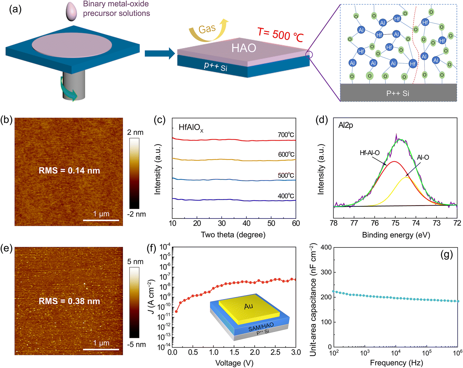 | ||
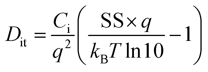
| Fig. 1 (a) Schematic drawing of the preparation process of HAO dielectrics. The inset is the schematic of the bonding state of the HAO dielectric based on the NAN process. (b) AFM image of the HAO dielectric. The annealing temperature was 500 °C. (c) XRD patterns of the HAO dielectric at different annealing temperatures. (d) Al 2p XPS spectrum of the HAO dielectric treated by the NAN process. (e) AFM image of the HAO dielectric after modification by SAM. (f) Leakage current density of the SAM/HAO dielectric. The inset is the schematic of the capacitor device. (g) Unit-area capacitance of the SAM/HAO dielectric. | ||
The atomic force microscope (AFM) images of the HAO dielectric are shown in Fig. 1b, which exhibited an ultra-flat surface with a root-mean-square (RMS) roughness of 0.14 nm. The X-ray diffraction (XRD) spectrum showed that the film was amorphous in a wide temperature range from 400 °C to 700 °C (Fig. 1c). In sharp contrast, the single-component system of HfOx began to crystallize at 400 °C, and as the annealing temperature was increased, the intensity of the XRD peak increased significantly (Fig. S4a, ESI†). It was determined that the peak position belonged to the monoclinic crystal orientation of HfOx. By comparison, the leakage current of the HAO dielectric showed four orders of magnitude lower than that of the HfOx dielectric at 3 V (Fig. S4b, ESI†). This illustrated that the formation of binary alloy oxides could effectively inhibit crystallization and reduce leakage.
X-ray photoelectron spectroscopy (XPS) was performed to explore the bonding conditions of the binary metal oxides. From the Al 2p core level spectra shown in Fig. 1d and Fig. S5a (ESI†), the spectra were deconvoluted into two peaks located at binding energies of 75.0 eV and 74.4 eV, attributed to the bonds of Hf–Al–O and Al–O, respectively. This variation in bonding formation and the amorphous structure of the film may cause the dielectric constant of the HAO dielectric to deviate from the trend deduced from principle.30,31 For the HAO dielectric treated by the NAN process (Fig. 1d), the HfAlOx alloy was obviously dominant with a small amount of Al–O bonds. In contrast, the content of Al–O bonds in HAO dielectrics fully annealed in nitrogen was much higher (Fig. S5a, ESI†). This further proved that the use of the NAN process contributed to the effective bonding of the binary metal oxide. As a comparison, the leakage current density of the HAO dielectric treated by the NAN process was nearly two orders of magnitude lower than that of the HAO dielectric treated with nitrogen (Fig. S5b, ESI†). In addition, the unit-area capacitance of the HAO dielectric treated by the NAN process showed ultra-low frequency dependence (Fig. S5c, ESI†). The above facts illustrated that controlling the bonding mode could effectively improve the quality of the binary dielectric film.32,33
SAMs have been widely used to passivate the surface of metal oxide dielectrics to eliminate the adverse effects of dangling bonds and hydroxyl groups on carrier transport.19 Here, we adopted octadecylphosphonic acid (ODPA) as the SAM. After modification, the film exhibited typical hydrophobicity with a water contact angle of 108° (Fig. S6, ESI†), indicating a good modification quality. Characterized by AFM, the dielectric surface after the SAM modification still exhibited a very smooth surface (RMS = 0.38 nm) (Fig. 1e). The total thickness of the HAO dielectric combined with the SAM was shown as 23 nm characterized by scanning electron microscopy (SEM) (Fig. S7, ESI†). Capacitor devices were fabricated by evaporating Au electrodes with an area of 200 × 200 μm2 onto the HAO dielectric. The leakage current density was shown as 5.5 × 10⁻⁸ A cm−2 at 3 V (1.3 MV cm−1) (Fig. 1f), which was very low among the solution-processed metal oxide dielectrics.34–37 The unit-area capacitance was measured as 204 nF cm−2 at 103 Hz and showed a negligible frequency dependence (Fig. 1g). The prepared high-quality binary metal oxide dielectrics laid a solid foundation for the pursuit of high-efficiency charge transport in low-voltage OFETs.
2.2 Few-layered two-dimensional molecular crystals (2DMCs) transferred to HAO dielectrics.
2DMCs are considered to be ideal channel layers for transistors, with significant advantages of long-range ordered molecular stacking, the absence of grain boundaries, the low density of defects and traps, and reduced contact resistance.37–39 Recently, liquid substrates have been successfully developed for growing 2DMCs, and this strategy has shown good applicability for a variety of organic semiconductors due to its effective elimination of the coffee ring effect.37 In this work, we prepared a typical molecule, 2,6-bis(4-hexylphenyl)anthracene (C6-DPA), into a large-area of 2DMCs with a thickness of several molecular layers on the surface of glycerol. The semi-freestanding feature of the 2DMCs of C6-DPA on the glycerin surface allowed it to be well transferred to the as-prepared SAM/HAO dielectric, as shown in Fig. 2a. Fig. 2b and c show the polarized optical microscopy (POM) images. When the sample was rotated by 45°, the entire crystal exhibited an obvious and uniform color change, indicating its single crystalline nature. The AFM image showed that the RMS of the crystal was 0.23 nm, indicative of the atomically flat surface (Fig. 2d). And the thickness was measured as 8.9 nm that corresponded to three molecular layers.41 As shown in Fig. 2e, the molecular packing of the C6-DPA crystal was characterized by high-resolution AFM (HRAFM). Lattice constants of a = 6.32 Å, b = 8.18 Å, and θ = 86.5° were obtained, consistent with previous reports.41 The XRD pattern exhibited three sharp peaks proving the high crystallinity of the crystal (Fig. 2f). As shown in Fig. 2g, a typical transmission electron microscopy (TEM) image revealed a uniform morphology. The selected area electron diffraction (SAED) pattern (Fig. 2h–j) showed ordered and bright diffraction spots over the entire crystal, further confirming the single crystal nature of the 2DMCs of C6-DPA.41 | ||
| Fig. 2 (a) Optical microscopy (OM) image of a 2DMC of C6-DPA. (b) and (c) POM image of a 2DMC of C6-DPA. (d) AFM image of a 2DMC of C6-DPA. (e) HRAFM image of a 2DMC of C6-DPA. (f) XRD patterns of a 2DMC of C6-DPA. (g) and (h–j) TEM images and the corresponding SAED patterns of a 2DMC of C6-DPA. | ||
2.3 Electrical properties of low-voltage transistors
To evaluate the performance of OFETs based on SAM/HAO dielectrics, the transistor devices with a typical bottom-gate top-contact (BGTC) configuration were fabricated by transferring the “Au film” on 2DMCs using a mechanical probe. This nondestructive method of van der Waals assembling electrodes is very important for vulnerable, ultrathin molecular crystals, which can produce a high quality ohmic contact when the energy level between the electrode and the semiconductor is matched.42–44Typical transfer and output characteristic curves are shown in Fig. 3a and b, which exhibited a low operating voltage of −3 V, an on-state saturation current of >2 μA, and a high on/off ratio of 107. Note that the off-state current of the transistor was as low as 10−13 A, which could be attributed to the good insulation quality of the HAO dielectric. Impressively, the average mobility of 30 devices was 1.9 cm2 V−1 s−1, and the highest mobility was 3.0 cm2 V−1 s−1 (Fig. 3c and Fig. S8 (ESI†)), which was among the highest values of mobility reported for C6-DPA.37,39–41 In contrast, the mobility performance of OFETs fabricated on high-k metal oxide dielectrics was significantly lower than those prepared using OTS-modified SiO2 substrates in previous reports (Table S1, ESI†).
 | ||
| Fig. 3 (a) Typical transfer I–V curve of the C6-DPA based OFET. The inset shows the device configuration of the OFET. (b) Output characteristics of the C6-DPA based OFET. The channel length was 135 μm, and the channel width was 180 μm. (c) Mobility statistics of 30 devices. (d) SS statistics of 27 devices. (e) SS versus IDS characteristics of the C6-DPA based OFET. (f) Total resistance obtained by the transmission line method (TLM) as a function of the channel length under a −3 V gate voltage, where y-intercept is the contact resistance. | ||
Furthermore, the transistors exhibited a uniform Vth (Fig. S9, ESI†) and steep sub-threshold swing. The average sub-threshold swing of 27 devices was 61 mV dec−1, and the lowest sub-threshold slope was 60 mV dec−1 (Fig. 3d and e), which approached the Boltzmann limit at room temperature.45,46 According to eqn (1), the interface trap state density (Dit) was determined to be 1.81 × 10¹⁰ eV cm−2, which was at least an order of magnitude lower than the recently reported low-voltage OFETs (Table S2, ESI†).
 | (1) |
The contact resistance extracted using the transmission line method (TLM)37 was shown as 1.15 kΩ cm at a gate voltage of −3 V (Fig. 3f). Note that the energy levels between Au and C6-DPA were not well matched, and the contact resistance was expected to be further reduced by inserting doping layers such as F4-TCNQ, pentaflfluorobenzenethiol (PFBT) between the semiconductor and the electrode.8,47 Thus, we give a high benchmark of performance for OFETs based on high-k dielectrics, providing promising candidates for future low-power electronic applications.
For comparison, we also modified the SAM (ODPA) on the HAO whose bonding mode was not optimized (i.e., the annealing process was fully performed under nitrogen), and fabricated the transistor devices using the same semiconductor (C6-DPA). The devices exhibited an on/off ratio of 106, a sub-threshold swing of 97 mV dec−1, and the highest mobility of 1.6 cm2 V−1 s−1 (Fig. S11b, ESI†), and the output curve showed a larger contact resistance (Fig. S11c, ESI†). These performances were obviously lower than the devices prepared on the HAO whose bonding mode was controlled. This suggested that controlling the bonding mode of binary metal oxide dielectrics contributes to the realization of OFETs.
To examine the applicability of the SAM/HAO dielectric, we have also grown n-type ultrathin molecular crystal, a furan-thiophene quinoidal compound (TFT-CN), on the surface of glycerol. The OFETs were enabled by transferring the n-type 2DMCs onto the SAM/HAO dielectric. The devices also exhibited excellent electrical properties including a low operation voltage of 2 V, a large on/off ratio of 107, and a steep sub-threshold swing of 82 mV dec−1 (Fig. S12, ESI†). And importantly, the mobility of 0.9 cm2 V−1 s−1 was also comparable to those fabricated using OTS-modified SiO2 dielectrics.44 This indicates that the developed binary metal oxide dielectrics exhibit good applicability for both p-type and n-type semiconductors.
2.4 Inverters based on dual-channel p–n heterojunctions
In order to evaluate the potential of the obtained low-voltage OFETs in logic circuits, ambipolar organic field-effect transistors (aOFETs) based on p–n heterojunctions (C6-DPA as a p-type semiconductor and TFT-CN as a n-type semiconductor) were prepared to construct complementary-like inverters (Fig. 4a). The p–n heterojunctions were fabricated on the HAO dielectric layer by a typical layer-by-layer transfer process of two types of 2DMCs.48 The fluorescence image of a p–n heterojunction is shown in Fig. 4b. It was observed that typical fluorescence quenching occurred in the overlap region owing to the spontaneous charge transfer between the p-type C6-DPA and the n-type TFT-CN. The homogeneous quenching color of the entire heterojunction implied its excellent uniformity.48 The AFM image of the heterojunction (Fig. 4c) showed clear boundaries and the overlapping of two types of 2DMCs. The thickness of the heterojunction was measured as 10.7 nm, which coincided with a sum of the thicknesses of 2DMCs of C6-DPA (8.9 nm) and TFT-CN (1.8 nm). XRD patterns (Fig. S13, ESI†) of the heterojunctions showed all the characteristic peaks of the single components, indicating the successful preparation of the single-crystalline heterojunctions. | ||
| Fig. 4 (a) Schematic diagram of a complementary-like inverter based on a dual-channel p–n heterojunction composed of 2DMCs. (b) Fluorescence image of the p–n heterojunction of 2DMCs. (c) AFM image of the p–n heterojunction of 2DMCs. (d) Typical output curves of the aOFET composed of 2DMC p–n heterojunctions. (e) Transfer characteristics of the complementary-like inverter based on the aOFET. (f) Gain of the complementary-like inverter based on the aOFET. | ||
As shown in Fig. 4d, the aOFET device showed a very balanced on-state saturation current, which was around 0.3 μA at a gate bias of ± 4 V. The mobility of the device was also balanced with 0.64 cm2 V−1 s−1 for holes and 0.36 cm2 V−1 s−1 for electrons (Fig. S14a and S14b, ESI†). These balanced characteristics are critical for obtaining high gain in complementary-like inverters.49
The schematic of the complementary-like inverter based on the p–n heterojunctions is shown in Fig. S14c (ESI†), which was the first demonstration of inverters based on the 2DMC p–n heterojunctions. Impressively, the inverter exhibited sharp switching with rail-to-rail output swings (Fig. 4e), showing the highest signal gain of 172 at 4 V (Fig. 4f). To the best of our knowledge, this is the highest gain of a complementary-like inverter based on organic p–n heterojunctions,50–52 and it is also one of the best results for inverters based on low-voltage OFETs (Table S3, ESI†).
3. Conclusions
In summary, we developed a new binary metal oxide with a controlled bonding mode, atomic-level surface and homogeneous amorphous characteristics. After depositing the SAM, the SAM/HAO demonstrated a high unit-area capacitance of 204 nF cm−2 and a low leakage current density of 5.5 × 10⁻⁸ A cm−2 at 3 V (1.3 MV cm−1). Combined with few-layered molecular crystals of C6-DPA, the developed low-voltage OFETs exhibited remarkable performance including the highest (average) mobility of 3.0 (1.9) cm2 V−1 s−1, a steep SS of 60 mV dec−1 reaching the theoretic limit at room temperature, an on/off ratio of 107, an operation voltage of 3 V, and negligible hysteresis properties. The combination of the SAM/HAO dielectric and the n-type 2DMCs also achieved similar good results. On this basis, aOFETs based on dual-channel p–n heterojunctions (C6-DPA as a p-type semiconductor and TFT-CN as a n-type semiconductor) were prepared to construct complementary-like inverters, which showed a remarkably high gain of 172 (VDD = 4 V). These results indicate that OFETs based on high-k dielectrics can obtain good applications through a binary metal oxide dielectric (HAO) whose bonding mode was controlled. This study provides promising candidates for future integrated applications.4. Experimental section
Materials
2,6-Bis(4-hexylphenyl)anthracene (C6-DPA, Fig. S11, ESI†) and furan-thiophene quinoidal compound (TFT-CN, Fig. S12, ESI†) were purchased from Lumtec. Hafnium(IV) iso-propoxide (Hf(C3H7O)4) was purchased from Alfa-Aesar. Aluminum sec-butoxide (Al(C4H9O)3) was purchased from TCI. 2-Methoxyethanol was purchased from Sigma-Aldrich. All materials were used without purification.Preparation of precursor solution
The precursor solutions of HAO were prepared using Al(C4H9O)3 and Hf(C3H7O)4 under a nitrogen atmosphere, and then dissolved in 2-methoxyethanol. The total concentration of the precursor in the solution was 0.22 mol L−1, and the molar composition ratio of the HAO precursor solution was Hf/Al = 1![[thin space (1/6-em)]](https://www.rsc.org/images/entities/char_2009.gif) :1. The ratio of Hf and Al was optimized for obtaining high-k and low leakage dielectrics. Next, the solutions were vigorously stirred for 12 h at 75 °C.
:1. The ratio of Hf and Al was optimized for obtaining high-k and low leakage dielectrics. Next, the solutions were vigorously stirred for 12 h at 75 °C.
Preparation of HAO thin films
HAO thin films were prepared by depositing precursor solutions onto the Si substrates through 0.22 μm PTFE filters followed by a spin-coating process with rotation at 4000 rpm for 30 s. Then, the HAO thin films were annealed by a “nitrogen–air–nitrogen (NAN)” process and cooling to room temperature.Formation of the self-assembled monolayer (SAM)
To form the SAM layer of phosphonic acids, HAO-coated Si substrates were treated with oxygen plasma for 10 min and then soaked in a solution of octadecylphosphonic acid (ODPA) in isopropyl alcohol (1.5 mM) at 60 °C for 12 h in air atmosphere, and then ultrasonically cleaned with chloroform, n-hexane, and isopropanol for 5 min each and dried under a nitrogen flow.OFET construction
For the fabrication of OFETs, 2D molecular crystals (2DMCs) were grown on the liquid substrate and then transferred onto the surface of the SAM/HAO. The device with a bottom-gate/top-contact (BGTC) configuration was prepared by stamping Au (150 nm thickness) electrodes on the 2DMCs as the source and drain electrodes.Inverter construction
The 2DMCs of C6-DPA and TFT-CN were grown on the glycerol surface separately. The p-type semiconductor C6-DPA was transferred onto an SAM/HAO substrate. The 2DMCs of TFT-CN were transferred onto the SAM/HAO substrate pre-covered by the 2DMCs of C6-DPA to form the few-layered single-crystalline heterojunctions. Then Au (150 nm) stripes were stamped on the heterojunctions.Instrumentation and characterization
X-ray photoelectron spectroscopy (XPS) results were obtained using a Thermo ESCALAB 250XI x-ray photoelectron spectrometer with Al kα ray. The X-ray diffraction (XRD) results were obtained using a Rigaku SmartLab X-ray diffractometer with the highest power of 9 kW (step size 0.01°). Fourier transform infrared spectroscopy (ATR-FT IR, Vertex 70, Bruker) was performed to investigate the chemical structure of the HAO films. The atomic force microscopy (AFM) images were obtained in the tapping-mode using a Bruker Dimension Icon in air. The frequency dependence of the unit-area capacitance and the leakage current of the dielectric were measured using a Keithley 4200 SCS semiconductor parameter analyser in air. The OFETs and inverters were also measured using a Keithley 4200 SCS semiconductor parameter analyser in air. The mobility of the OFETs was calculated from the following equation: IDS = (W/2L)μCi(VG − Vth)2, where IDS is the source-drain current, μ is the field effect mobility, Vth is the threshold voltage, VG is the applied gate voltage, L is the channel length, W is the channel width and Ci is the specific capacitance (204 nF cm−2).Author contributions
R. Li, F. Yang and W. Hu conceived the idea and directed the project. C. Ma carried out the preparation of the Hf–Al–O bonded HAO thin film. Y. Zhang prepared the 2DMCs and fabricated OFETs and measured the electrical properties. B. Li carried out the construction and test of inverters. J. Wang was in charge of capacitance measurements. L. Sun, Y. Liu, X. Tian and J. Yao helped to test the SAED of 2DMCs. Z. Wang and S. Li helped to test the XPS spectrum. All the authors analysed the experimental results and contributed to the discussion.Conflicts of interest
There are no conflicts to declare.Acknowledgements
The authors thank the National Key R&D Program (2022YFB3607500), the National Natural Science Foundation of China (No. 51903186, 51873148, 52073206 and 51633006), the open research fund from State Key Laboratory of Luminescent Materials and Devices (2023-skllmd-02), the Tianjin Science Foundation (20JCQNJC01990) and the Haihe Laboratory of Sustainable Chemical Transformations.References
- J. Yang, Q. Liu, M. Hu, S. Ding, J. Liu, Y. Wang, D. Liu, H. Gao, W. Hu and H. Dong, Sci. China: Chem., 2021, 64, 1410–1416 CrossRef CAS.
- Z. Qin, H. Gao, H. Dong and W. Hu, Adv. Mater., 2021, 33, 2007149 CrossRef CAS PubMed.
- Y. Yao, Y. Chen, H. Wang and P. Samorì, SmartMat, 2020, 1, e1009 CrossRef.
- B. Fu, F. Yang, L. Sun, Q. Zhao, D. Ji, Y. Sun, X. Zhang and W. Hu, Adv. Mater., 2022, 34, 2203330 CrossRef CAS PubMed.
- X. Zhu, Y. Yan, L. Sun, Y. Ren, Y. Zhang, Y. Liu, X. Zhang, R. Li, H. Chen, J. Wu, F. Yang and W. Hu, Adv. Mater., 2022, 34, 2201364 CrossRef CAS PubMed.
- X. Ren, F. Yang, X. Gao, S. Cheng, X. Zhang, H. Dong and W. Hu, Adv. Energy Mater., 2018, 8, 1801003 CrossRef.
- H. Chen, S. Dong, M. Bai, N. Cheng, H. Wang, M. Li, H. Du, S. Hu, Y. Yang, T. Yang, F. Zhang, L. Gu, S. Meng, S. Hou and X. Guo, Adv. Mater., 2015, 27, 2113–2120 CrossRef CAS PubMed.
- J. W. Borchert, B. Peng, F. Letzkus, J. N. Burghartz, P. K. L. Chan, K. Zojer, S. Ludwigs and H. Klauk, Nat. Commun., 2019, 10, 1119 CrossRef PubMed.
- X. Ren, Z. Lu, X. Zhang, S. Grigorian, W. Deng and J. Jie, ACS Mater. Lett., 2022, 4, 1531–1546 CrossRef CAS.
- F. Yang, L. Sun, Q. Duan, H. Dong, Z. Jing, Y. Yang, R. Li, X. Zhang, W. Hu and L. Chua, SmartMat, 2021, 2, 99–108 CrossRef CAS.
- F.-D. Wang, M.-X. Yu, X.-D. Chen, J. Li, Z.-C. Zhang, Y. Li, G.-X. Zhang, K. Shi, L. Shi, M. Zhang, T.-B. Lu and J. Zhang, SmartMat, 2023, 4, e1135 CAS.
- J. Ouyang, SmartMat, 2021, 2, 263–285 CrossRef CAS.
- N. S. Kim, T. M. Austin, D. Blaauw, T. N. Mudge, K. Flautner, J. S. Hu, M. J. Irwin, M. T. Kandemir and N. Vijaykrishnan, Computer, 2003, 36, 68–75 Search PubMed.
- A. Facchetti, M.-H. Yoon and T. J. Marks, Adv. Mater., 2005, 17, 1705–1725 CrossRef CAS.
- R. Ponce Ortiz, A. Facchetti and T. Marks, Chem. Rev., 2009, 110, 205–239 CrossRef PubMed.
- B. Fu, L. Sun, L. Liu, D. Ji, X. Zhang, F. Yang and W. Hu, Sci. China Mater., 2022, 65, 2779–2785 CrossRef CAS.
- B. Wang, W. Huang, L. Chi, M. Al-Hashimi, T. J. Marks and A. Facchetti, Chem. Rev., 2018, 118, 5690–5754 CrossRef CAS PubMed.
- Q. Mu, Z. Chen, S. Duan, X. Zhang, X. Ren and W. Hu, Front. Mater., 2020, 7, 570002 CrossRef.
- O. Acton, G. Ting, H. Ma, J. W. Ka, H.-L. Yip, N. M. Tucker and A. K.-Y. Jen, Adv. Mater., 2008, 20, 3697–3701 CrossRef CAS.
- W. He, W. Xu, Q. Peng, C. Liu, G. Zhou, S. Wu, M. Zeng, Z. Zhang, X. Gao, X. Lu and J.-M. Liu, J. Phys. Chem. C, 2016, 120, 9949–9957 CrossRef CAS.
- Z. Luo, B. Peng, J. Zeng, Z. Yu, Y. Zhao, J. Xie, R. Lan, Z. Ma, L. Pan, K. Cao, Y. Lu, D. He, H. Ning, W. Meng, Y. Yang, X. Chen, W. Li, J. Wang, D. Pan, X. Tu, W. Huo, X. Huang, D. Shi, L. Li, M. Liu, Y. Shi, X. Feng, P. K. L. Chan and X. Wang, Nat. Commun., 2021, 12, 1928 CrossRef PubMed.
- M. Geiger, R. Lingstädt, T. Wollandt, J. Deuschle, U. Zschieschang, F. Letzkus, J. N. Burghartz, P. A. van Aken, R. T. Weitz and H. Klauk, Adv. Electron. Mater., 2022, 8, 2101215 CrossRef CAS.
- L. Zhu, Y. Gao, X. Li, X. W. Sun and J. Zhang, J. Mater. Res., 2014, 29, 1620–1625 CrossRef CAS.
- S. H. Bae, C. H. Lee, R. Clark and D. L. Kwong, IEEE Electron Device Lett., 2003, 24, 556–558 CAS.
- H. Sirringhaus, Adv. Mater., 2009, 21, 3859–3873 CrossRef CAS.
- I. N. Hulea, S. Fratini, H. Xie, C. L. Mulder, N. N. Iossad, G. Rastelli, S. Ciuchi and A. F. Morpurgo, Nat. Mater., 2006, 5, 982–986 CrossRef CAS PubMed.
- J. Veres, S. D. Ogier, S. W. Leeming, D. C. Cupertino and S. Mohialdin Khaffaf, Adv. Funct. Mater., 2003, 13, 199–204 CrossRef CAS.
- K. Norrman, A. Ghanbari-Siahkali and N. B. Larsen, Annu. Rep. Prog. Chem., 2005, 101, 174–201 RSC.
- S. Park, C.-H. Kim, W.-J. Lee, S. Sung and M.-H. Yoon, Mater. Sci. Eng., R, 2017, 114, 1–22 CrossRef.
- G. D. Wilk, R. M. Wallace and J. M. Anthony, J. Appl. Phys., 2001, 89, 5243–5275 CrossRef CAS.
- G. Lucovsky and G. B. Rayner Jr., Appl. Phys. Lett., 2000, 77, 2912–2914 CrossRef CAS.
- G. He, L. D. Zhang, G. W. Meng, G. H. Li, Q. Fang and J. P. Zhang, J. Appl. Phys., 2007, 102, 094103 CrossRef.
- J. Gao, G. He, M. Liu, J. G. Lv, Z. Q. Sun, C. Y. Zheng, P. Jin, D. Q. Xiao and X. S. Chen, J. Alloys Compd., 2017, 691, 504–513 CrossRef CAS.
- Q. Zhang, G. Xia, W. Xia, J. Zhou and S. Wang, Synth. Met., 2015, 210, 282–287 CrossRef CAS.
- D.-K. Kim, M. Lee, B. Kim and J.-H. Choi, Org. Electron., 2019, 74, 135–143 CrossRef CAS.
- J.-D. Oh, J.-W. Kim, D.-K. Kim and J.-H. Choi, Org. Electron., 2016, 30, 131–135 CrossRef CAS.
- Q. Wang, F. Yang, Y. Zhang, M. Chen, X. Zhang, S. Lei, R. Li and W. Hu, J. Am. Chem. Soc., 2018, 140, 5339–5342 CrossRef CAS PubMed.
- L. Jiang, J. Liu, Y. Shi, D. Zhu, H. Zhang, Y. Hu, J. Yu, W. Hu and L. Jiang, J. Mater. Chem. C, 2019, 7, 3436–3442 RSC.
- Z. Chen, S. Duan, X. Zhang and W. Hu, Sci. China: Chem., 2021, 64, 1057–1062 CrossRef CAS.
- C. Xu, P. He, J. Liu, A. Cui, H. Dong, Y. Zhen, W. Chen and W. Hu, Angew. Chem., Int. Ed., 2016, 55, 9519–9523 CrossRef CAS PubMed.
- J. Yao, Y. Zhang, X. Tian, X. Zhang, H. Zhao, X. Zhang, J. Jie, X. Wang, R. Li and W. Hu, Angew. Chem., Int. Ed., 2019, 58, 16082–16086 CrossRef CAS PubMed.
- Q. Tang, Y. Tong, H. Li, Z. Ji, L. Li, W. Hu, Y. Liu and D. Zhu, Adv. Mater., 2008, 20, 1511–1515 CrossRef CAS.
- Q. Tang, L. Jiang, Y. Tong, H. Li, Y. Liu, Z. Wang, W. Hu, Y. Liu and D. Zhu, Adv. Mater., 2008, 20, 2947–2951 CrossRef CAS.
- B. Peng, K. Cao, A. H. Y. Lau, M. Chen, Y. Lu and P. K. L. Chan, Adv. Mater., 2020, 32, 2002281 CrossRef CAS PubMed.
- F. Yang, L. Sun, J. Han, B. Li, X. Yu, X. Zhang, X. Ren and W. Hu, ACS Appl. Mater. Interfaces, 2018, 10, 25871–25877 CrossRef PubMed.
- A. M. Ionescu and H. Riel, Nature, 2011, 479, 329–337 CrossRef CAS PubMed.
- Y. Kim, S. Chung, K. Cho, D. Harkin, W.-T. Hwang, D. Yoo, J.-K. Kim, W. Lee, Y. Song, H. Ahn, Y. Hong, H. Sirringhaus, K. Kang and T. Lee, Adv. Mater., 2019, 31, 1806697 CrossRef PubMed.
- X. Tian, J. Yao, L. Zhang, B. Han, J. Shi, J. Su, J. Liu, C. Li, X. Liu, T. Zhai, L. Jiang, F. Yang, X. Zhang, Y. Zou, R. Li and W. Hu, Nano Res., 2022, 15, 2667–2673 CrossRef CAS.
- T. Leydecker, Z. M. Wang, F. Torricelli and E. Orgiu, Chem. Soc. Rev., 2020, 49, 7627–7670 RSC.
- S. Yadav and S. Ghosh, AIP Conf. Proc., 2013, 1512, 466–467 CrossRef CAS.
- D. Panigrahi, R. Hayakawa, K. Honma, K. Kanai and Y. Wakayama, Appl. Phys. Express, 2021, 14, 081004 CrossRef CAS.
- M.-J. An, H.-S. Seo, Y. Zhang, J.-D. Oh and J.-H. Choi, Appl. Phys. Lett., 2010, 97, 023506 CrossRef.
Footnotes |
| † Electronic supplementary information (ESI) available. See DOI: https://doi.org/10.1039/d3tc00246b |
| ‡ C. Ma, B. Li and Y. Zhang contributed equally to this work. |
| This journal is © The Royal Society of Chemistry 2023 |