
 Open Access Article
 This Open Access Article is licensed under a Creative Commons Attribution-Non Commercial 3.0 Unported Licence
Quantitative mechanics of 3D printed nanopillars interacting with bacterial cells
Mahya
Ganjian
 *a,
Livia
Angeloni
ab,
Mohammad J.
Mirzaali
a,
Khashayar
Modaresifar
a,
Cornelis W.
Hagen
c,
Murali K.
Ghatkesar
b,
Peter-Leon
Hagedoorn
d,
Lidy E.
Fratila-Apachitei
a and
Amir A.
Zadpoor
a
*a,
Livia
Angeloni
ab,
Mohammad J.
Mirzaali
a,
Khashayar
Modaresifar
a,
Cornelis W.
Hagen
c,
Murali K.
Ghatkesar
b,
Peter-Leon
Hagedoorn
d,
Lidy E.
Fratila-Apachitei
a and
Amir A.
Zadpoor
a
aDepartment of Biomechanical Engineering, Faculty of Mechanical, Maritime, and Materials Engineering, Delft University of Technology, Mekelweg 2, 2628CD, Delft, The Netherlands. E-mail: m.ganjian@tudelft.nl
bDepartment of Precision and Microsystems Engineering, Faculty of Mechanical, Maritime, and Materials Engineering, Delft University of Technology, Mekelweg 2, 2628CD, Delft, The Netherlands
cDepartment of Imaging Physics, Faculty of Applied Sciences, Delft University of Technology, Lorentzweg 1, 2628CJ, Delft, The Netherlands
dDepartment of Biotechnology, Faculty of Applied Sciences, Delft University of Technology, Van der Maasweg 9, 2629HZ, Delft, The Netherlands
First published on 4th September 2020
Abstract
One of the methods to create sub-10 nm resolution metal-composed 3D nanopillars is electron beam-induced deposition (EBID). Surface nanotopographies (e.g., nanopillars) could play an important role in the design and fabrication of implantable medical devices by preventing the infections that are caused by the bacterial colonization of the implant surface. The mechanical properties of such nanoscale structures can influence their bactericidal efficiency. In addition, these properties are key factors in determining the fate of stem cells. In this study, we quantified the relevant mechanical properties of EBID nanopillars interacting with Staphylococcus aureus (S. aureus) using atomic force microscopy (AFM). We first determined the elastic modulus (17.7 GPa) and the fracture stress (3.0 ± 0.3 GPa) of the nanopillars using the quantitative imaging (QI) mode and contact mode (CM) of AFM. The displacement of the nanopillars interacting with the bacteria cells was measured by scanning electron microscopy (50.3 ± 9.0 nm). Finite element method based simulations were then applied to obtain the force-displacement curve of the nanopillars (considering the specified dimensions and the measured value of the elastic modulus) based on which an interaction force of 88.7 ± 36.1 nN was determined. The maximum von Mises stress of the nanopillars subjected to these forces was also determined (3.2 ± 0.3 GPa). These values were close to the maximum (i.e., fracture) stress of the pillars as measured by AFM, indicating that the nanopillars were close to their breaking point while interacting with S. aureus. These findings reveal unique quantitative data regarding the mechanical properties of nanopillars interacting with bacterial cells and highlight the possibilities of enhancing the bactericidal activity of the investigated EBID nanopillars by adjusting both their geometry and mechanical properties.
1. Introduction
An increasing number of advanced nanotechnological applications require highly repeatable fabrication of ‘three-dimensional’ devices with complex and precisely-controlled geometries. Depending on the targeted feature size and the complexity of the desired geometry, nanofabrication techniques, such as two-photon polymerization (TPP),1 imprint lithography,2–5 interference lithography,6 3D molding,7 electron beam lithography (EBL),8–10 electron beam-induced deposition (EBID),10–13 ion beam lithography (IBL),14 or focused ion beam (FIB)10,15,16 could be used to fabricate such 3D structures.At the cutting-edge of nanotechnology, however, there is often a need for the fabrication of arbitrarily complex 3D geometries with few-nanometers resolution.17 EBID is currently the only nanofabrication technique that allows for combining 3D structures with few-nanometer (∼1 nm18) accuracy and repeatability. Given its (theoretical) sub-nanometer resolution and mask-free nature, EBID is a highly powerful yet straightforward technique for the fabrication of cutting-edge nanodevices.
EBID is performed inside a scanning electron microscope (SEM).19–22 The precursor molecules, which contain the material of interest, are introduced into the chamber. Then, the focused electron beam dissociates the precursor molecules into volatile products that leave the system and non-volatile products that form a deposit on the substrate. The gradual layer-by-layer addition of the deposited material creates the desired geometry that, as we have previously shown,13 can be very complex.23 In that sense, EBID is an ‘additive’ manufacturing technique and, thus, distinct from subtractive (e.g., RIE, FIB) and formative (e.g., 3D molding) techniques. Nanofeatures can be formed on any type of substrate. The wide choice of precursor gases makes EBID a powerful technique for different types of applications, including sensors,24–26 plasmonics,12,27 atomic force microscopy probes,17 superconductive nanowires,28 and the repair of UV lithography masks.29
Both the structural performance and functionality of the nanostructures made by EBID are dependent on the mechanical properties of the deposited material. Mechanobiological30 and antibacterial31–33 applications of nanopatterns highlight the ‘functional’ importance of understanding the mechanical behavior of EBID-made nanofeatures. For example, the mechanobiological consequences of the substrate stiffness for determining stem cell fate are currently being widely investigated.30,34,35 Dual-effect nanopatterns that simultaneously stimulate stem cell differentiation and kill bacteria are envisaged as well.36 As for antibacterial applications, the mechanical properties of the nanopillars have been shown to play a crucial role. Nanofeatures with very specific dimensions and aspect ratios are known to kill bacteria through pre-dominantly mechanical mechanisms (i.e., overstretching the bacterial cell wall and rupturing cells components due to cell wall penetration).33,36,37 In general, the capability of the nanofeatures to penetrate the cell wall can be ascribed to two factors: (i) the geometry of the tip, which must be as sharp as possible, and (ii) the mechanical properties of the nanostructures, which determine whether the nanofeatures can sustain the interaction force with bacteria without excessive deformation and, ultimately, failure. For such applications, it is important to understand the nanomechanical behavior of EBID-made structures. Moreover, the accurate determination of the mechanical properties of single nanopillars could allow one to estimate the interaction forces between the bacteria and nanopillars, enabling a better understanding of the killing mechanism of bacterial cells residing on nanopatterned surfaces.
In our previous studies, we have developed EBID-made nanopatterns with specific dimensions for antibacterial applications.32,33 We have found a killing efficiency of 97% against E. coli, but a lower killing efficiency (36.5%) against S. aureus.33 Given that the mechanical properties of single nanopillars influence their killing efficiency against bacterial cells,31,38 the mechanical characterization of the nanopillars is necessary to optimize our surfaces and to further understand the mechanisms involved in the bacteria-nanopatterns interaction.
Currently, however, the mechanical characterization of single EBID nanostructures is challenging and requires complex instrumentation consisting of advanced mechanical testing machines (e.g., AFM or nanoindenters) mounted inside SEM chambers. Some studies39–42 have investigated the mechanical behavior of EBID-made nanostructures by using this combination of instruments. For instance, Friedli et al.39 have applied bending tests using an AFM tip installed inside an SEM machine to determine the force constant and the resonance frequency of high aspect ratio vertical nanopillars grown by EBID from the organometallic precursor Cu(C5HF6O2)2·xH2O. They have demonstrated that the elastic modulus of the EBID deposited pillars is proportional to the acceleration voltage and the electron dosage used during the deposition. In another study, Lewis et al.41 measured the elastic modulus of EBID-deposited 3D nanostructures (precursor: MeCpPt(IV)Me3) by compression and bending tests using a nanoindentation system installed in an SEM chamber. The compression tests resulted in values in the range of 8.6–10.5 GPa for the elastic modulus of nanopillars. Their bending tests with the same setup resulted in a value of 15.2 GPa for the elastic modulus. Although these methods enable the user to measure the mechanical properties of EBID-deposited nanostructure with arbitrary shapes, they do not apply to conventional SEM machines, as a specific setup needs to be installed. Arnold et al.43 have measured the deflection of EBID deposited Pt–C nanopillars using a four-axis micromanipulator installed inside an SEM machine. The elastic modulus of the EBID nanopillars was then calculated by using nanopillars’ deflection as an input for finite element simulation. Their study was followed by an analysis of the effects of beam current and acceleration voltage on the elastic modulus of nanopillars. They concluded that at 30 kV and 5 kV as the voltage and the lowest beam current, nanopillars had the highest elastic modulus (i.e., 13 GPa).
The fracture stress of nanopillars deposited by EBID has, however, not been previously measured. Utke et al.42 measured the fracture stress on large volume structures deposited using Co2(CO)8 and Au(tfac)Me2 as precursors. Reiser et al.44 measured the stress at 7% strain of micro and nanopillars using nanoindentation and micro-compression, but not the fracture stress.
Here, we propose an approach for measuring the elastic modulus and fracture stress of EBID nanopillars without any need for any instrumentation beyond typical AFM. The elastic modulus was measured by quantitative imaging (QI) mode on individual pillars of different dimensions (height and diameter). The pillars were deposited using the same precursor, acceleration voltage, and beam current. The effects of the structure size and EBID deposition time on the elastic modulus of the material were investigated. We found a limited influence of the structure size and we concluded that the elastic modulus of EBID nanostructures can be measured by conventional AFM methods applied on larger structures deposited with the same deposition parameters. In addition, we estimated the maximum (fracture) stress of the nanopillars using contact mode (CM) AFM.45 The force-displacement curves of the nanopillars were obtained with a finite element (FEM) model in which the measured value of the elastic modulus was assigned to the nanopillars material. With these characteristics and the displacement of the nanopillars available from the SEM image of nanopillars interacting with cultured bacteria, the interaction force between bacteria and individual nanopillars was calculated. We then compared the maximum stress of the nanopillars subjected to these forces with the maximum (fracture) stress of the nanopillars measured by AFM to evaluate their breaking strength and to elaborate on the possible approaches that could be used to optimize the design of nanopatterns and to improve their bactericidal behavior.
2. Results
2.1. Bacterial cell culture
In the case of the specimens prepared for bacterial cell culture, the EBID nanopillars covered a surface of 20 × 20 μm2 (Fig. 1a). The actual dimensions of the nanopillars were as follows: height = 180 ± 9 nm (mean ± SD), interspacing = 170 ± 3 nm, base diameter = 70 ± 5 nm (Fig. 1b). Upon contact with the cultured bacteria, a number of nanopillars underneath the bacterial cells were bent with an average lateral displacement of 50.3 ± 9.0 nm (Fig. 1c–f).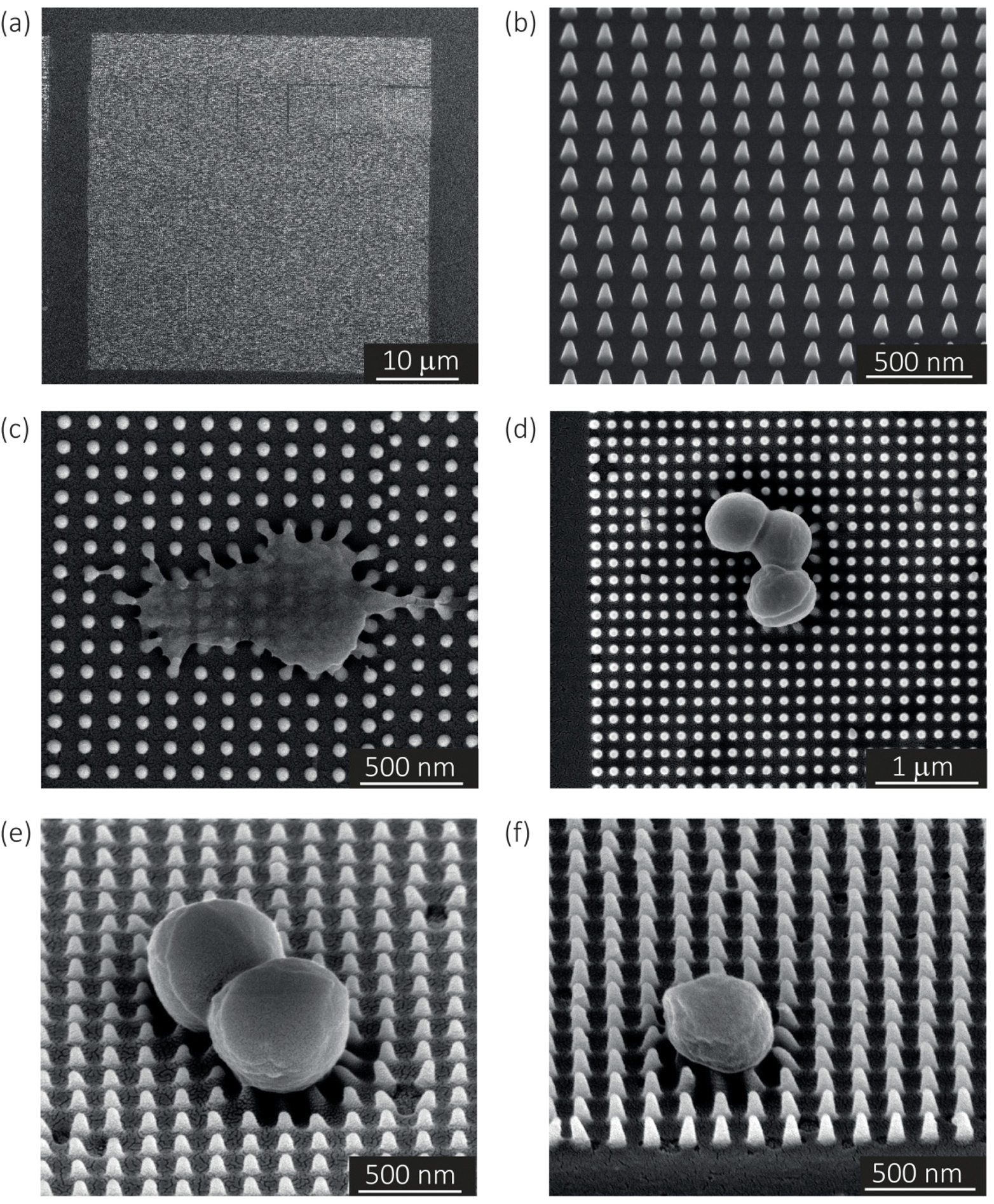 | ||
| Fig. 1 The SEM images of the nanopillars (with an average height of 180 nm, an average diameter of 70 nm, and average interspacing of 170 nm) produced by EBID at different magnifications: (a) top view and (b) 52°-tilted view. The SEM images of S. aureus bacteria on the nanopatterned surface: (c and d) the top and (e and f) 52°-tilted views. | ||
2.2. Elastic modulus of the pillars
Five pillars with different base diameters (d = 1500 nm, 1180 nm, 867 nm, 646 nm, and 433 nm) and heights of 383 ± 53 nm (Fig. 2a) and four pillars with diameters of 1112 ± 78 nm and different heights (Fig. 2b(1): h = 464 nm, Fig. 2b(2): h = 309 nm, Fig. 2c(3): h = 192 nm, Fig. 2c(4)h = 82 nm) (the left subfigures show the top view while the right subfigures were taken at a 52°-tilted view) were fabricated to obtain an almost flat region large enough to perform force spectroscopy mapping measurements (in the QI mode).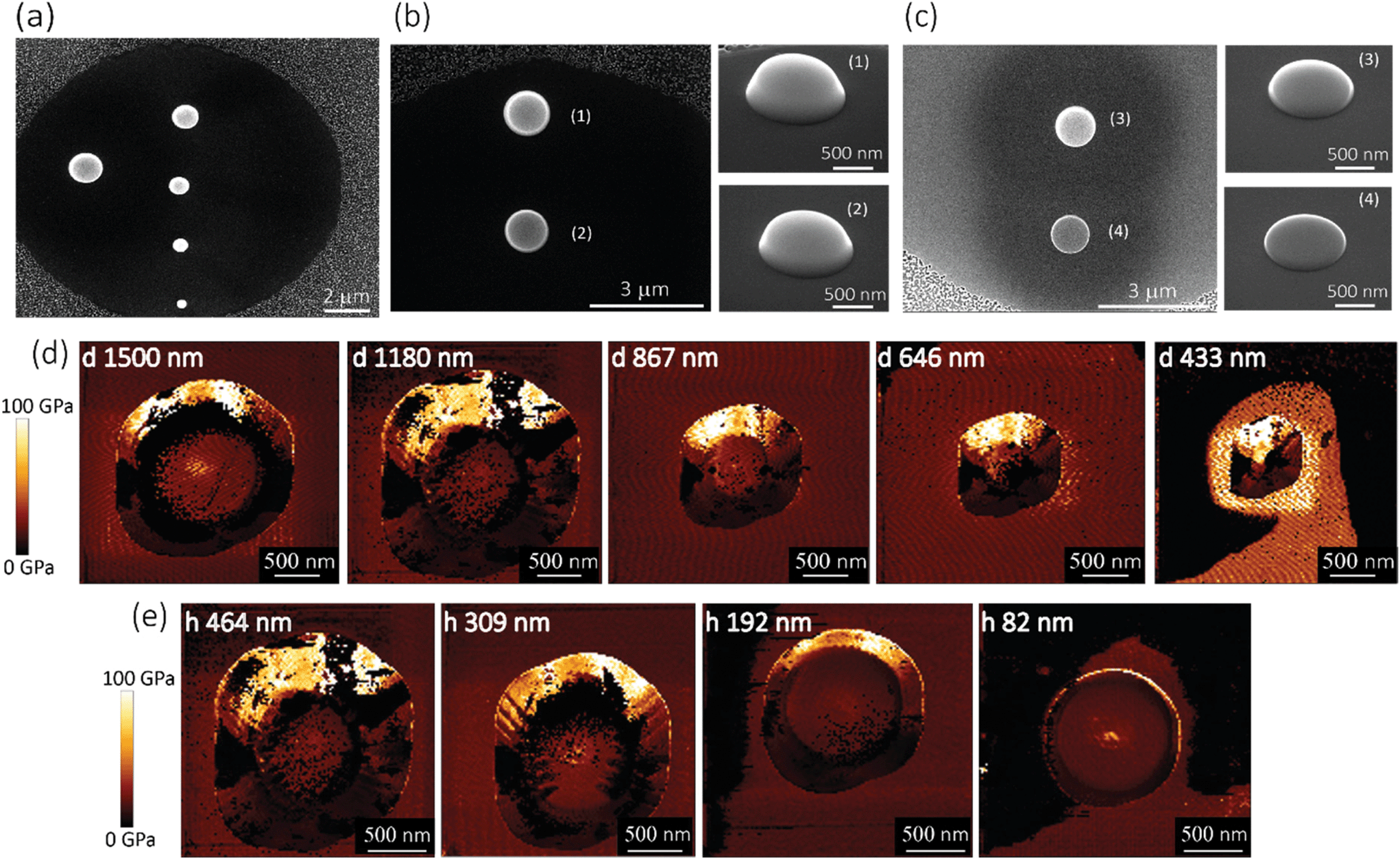 | ||
| Fig. 2 The SEM image of pillars with (a) different diameters: 433, 646, 867, 1180, and 1500 nm, (b and c) different heights: 1–464 nm, 2–309 nm, 3–192 nm, 4–82 nm. (The left figures were taken from the top view while the right figures were taken from 52°-tilted view.) (d) The map of the elastic modulus of the pillars with different diameters obtained by AFM. (e) The map of the elastic modulus of the pillars with different heights obtained by AFM. | ||
Above a certain distance from the pillar center, we observed a significant decrease (see the dark region at the bottom, left, and right sidewalls of the pillars) (Fig. 2d and e) or increase (bright part corresponding to the upper sidewall of the pillars) (Fig. 2d and e) in the measured values of the elastic modulus. This effect (underestimation/overestimation of the elastic modulus) can be explained by the fact that, when the tip-pillar contact occurred on the sidewalls of the pillar, it was asymmetric, causing the overestimation or underestimation of the contact area depending on the tilt angle of the cantilever and the position of the tip with respect to the pillar. Due to the pointy tip of one of the pillars (diameter = 433 nm), establishing symmetric contact between the AFM tip and the surface of the pillar was not feasible. Therefore, for this specific height (i.e., 383 nm), 646 nm was the minimum diameter for which the elastic modulus could be measured. The elastic modulus measured for the pillars with different heights and diameters varied between 15.9 GPa and 27.7 GPa (Fig. 3a and b).
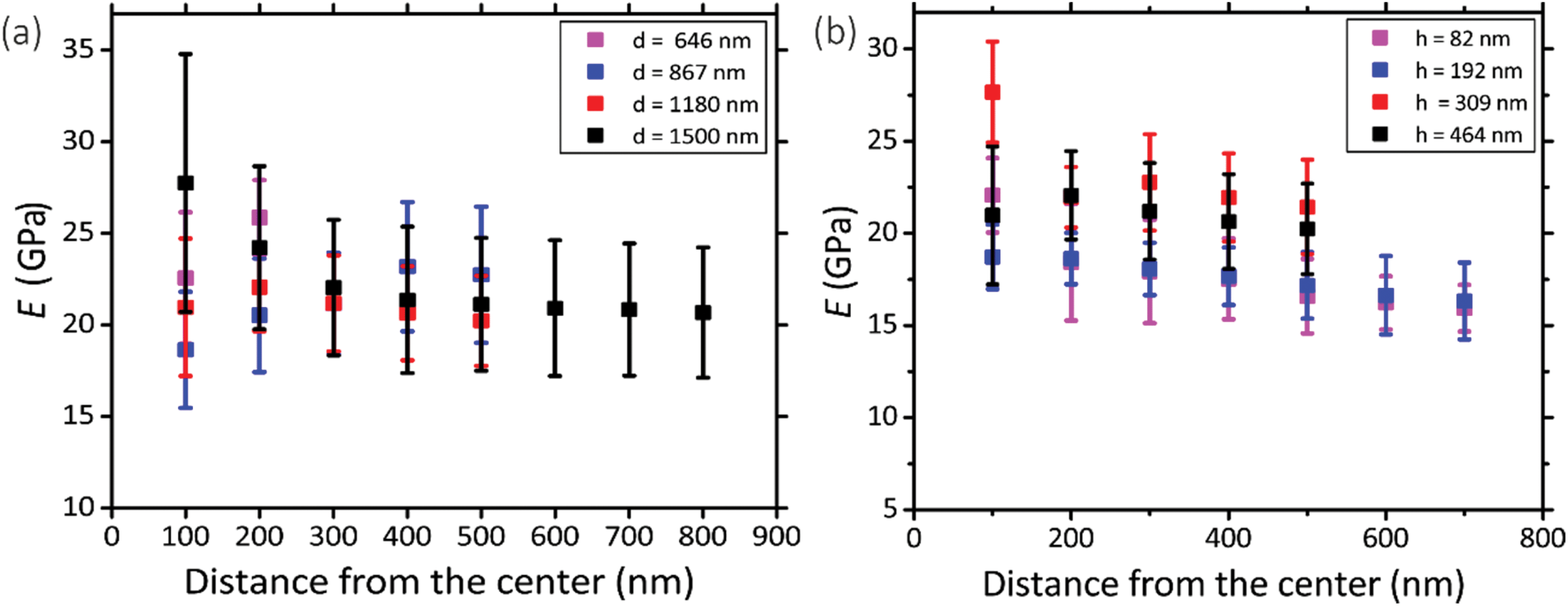 | ||
| Fig. 3 (a) The distribution of the elastic modulus for the pillars with different diameters in different distances from the center. (b) The distribution of the elastic modulus for the pillars with different heights (with the same diameter of 1000 nm) at different distances from the center. The pillars were deposited with an acceleration voltage of 17.8 kV and a current of 0.6 nA. | ||
Within the distance from the center for which the tip had symmetric contact with the surface of pillars, we did not observe a significant difference between the values of elastic modulus measured for different experimental groups (i.e., with different sizes) (Fig. 3a and b). The different parts of the surface exhibited similar values of the elastic modulus. A 200 nm distance from the center was the minimum distance that yielded a Gaussian distribution. We, therefore, did not consider smaller areas. The elastic modulus of the pillars with different diameters overlapped (Fig. 3a). The pillars with larger heights (i.e., 464 nm and 309 nm) exhibited slightly (but not significantly) higher values of the elastic modulus as compared to those with the lower heights (i.e., 192 nm and 82 nm) (Fig. 3b). In summary, no statistically significant changes in the value of the elastic modulus were observed for different values of the diameter of the deposited structures and different distances from the center. Only a slight difference (0.16%) with the height of the structure was observed. Therefore, the elastic modulus of our nanopillars can be assumed to be the same as the elastic modulus of the structure with a similar height (i.e., 192 nm). The elastic modulus measured for this structure was 17.7 ± 1.5 GPa.
2.3. Fracture stress
In the case of the specimens prepared for the measurement of the lateral detachment force, the nanopillars had the following dimensions: height = 196.5 ± 5.16 nm (measured by AFM), interspacing = 340 ± 1 nm in the x-direction and 1000 ± 100 nm in the y-direction, and base diameter = 68 ± 3 nm (Fig. 4a and b). A few representative images of the experiments performed to measure the fracture stress are presented in Fig. 4c–k. When low forces (e.g., Fsetpoint = 10 nN in the example reported in Fig. 4c–e) were applied, the fracture of the nanopillars was not visible in the CM images (Fig. 4c and d). A little (a few nm) change in the height of the nanopillars was observed in the QI mode images aquired with very low setpoint force before and after the application (Fig. 4e). This indicates that the failure of the nanopillars occurred at a height, which was very close to their apex. This is consistent with the mechanical behavior of a high aspect ratio conical structure. Indeed, when a lateral force is applied to the apex of a “sharp” conical pillar, the height of the point experiencing the maximum stress is closer to the apex of the pillar when the tip is smaller.45 Since the decrease of the height was low and difficult to measure with enough accuracy, larger forces were applied to the nanopillars by increasing the values of the applied setpoint forces. This procedure was repeated until the pillars were clearly observed to breake and the characteristics of their residues could be easily measured. In the presented example, a setpoint force (Flat) of 30 nN resulted in obvious fracture of two of the three nanopillars (Fig. 4f–h), for which a residue of about 26 nm was observed. Increasing the setpoint force not only increased the magnitude of the lateral force but also decreased the height at which the force was applied.45 For some of the nanopillars (e.g., the nanopillar in the center of the images in the reported example), no visible fracture was observed in the contact mode topographies with a setpoint of 30 nN (Fig. 4g), but only a further decrease of the height was visible in the QI mode topography images acquired after the application of the force in the CM (Fig. 4h). For those nanopillars, the setpoint force was further increased (50 nN in the reported example) (Fig. 4i–k).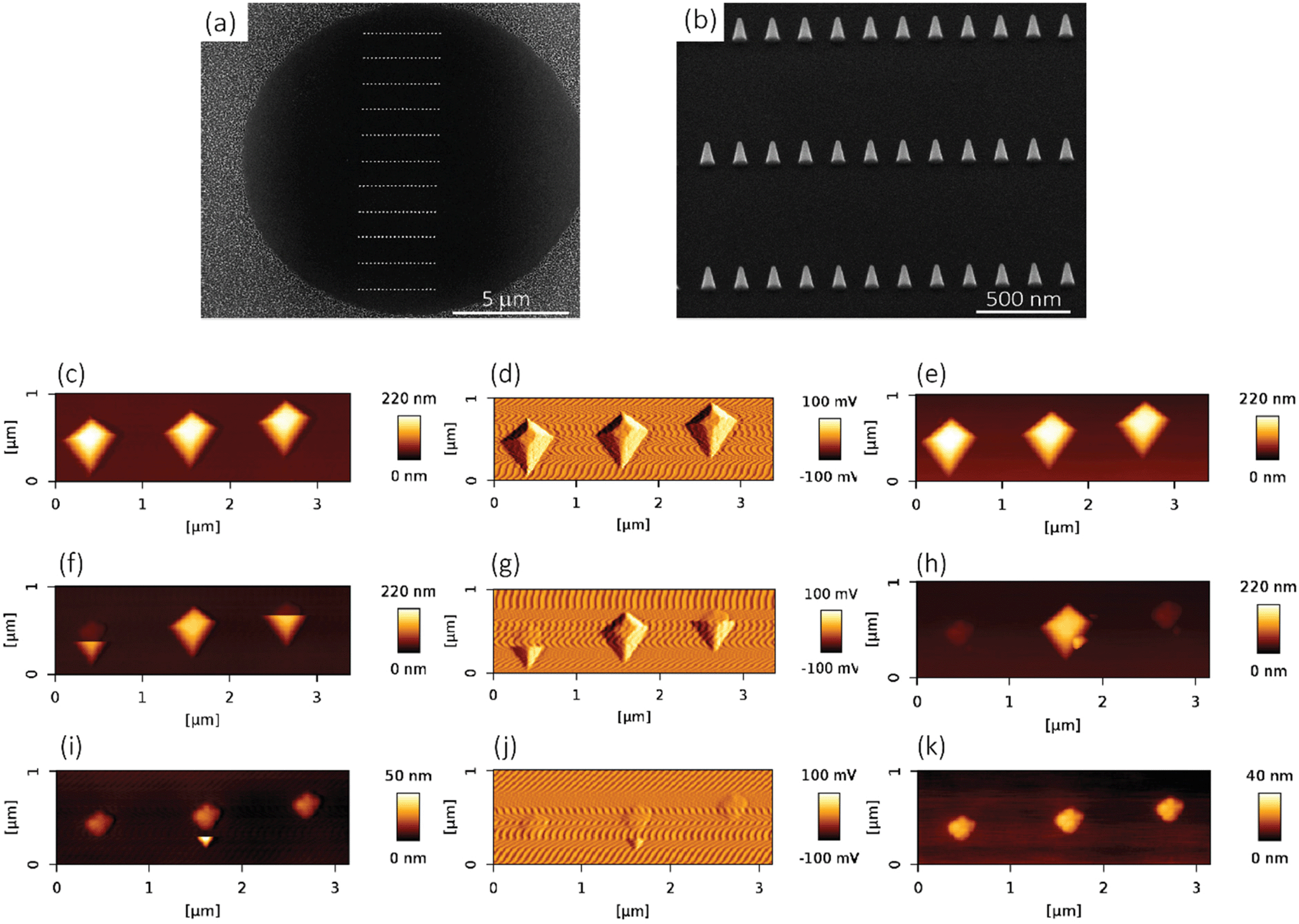 | ||
| Fig. 4 The SEM images of the rows of the nanopillars deposited by EBID to perform the mechanical experiments: (a) the top and (b) 52°-tilted views. (c, f and i) Contact mode topography images acquired with increasing values of setpoint forces (10 nN, 30 nN, and 50 nN, respectively); (d, g and j) vertical deflection error images acquired with increasing values of setpoint forces (10 nN, 30 nN, and 50 nN, respectively); (e, h and k) QI mode topography images acquired with a low, non-destructive, setpoint force (10 nN) after each contact mode scan with increasing values of the setpoint force (10 nN, 30 nN, and 50 nN, respectively). | ||
The values of the setpoint forces at which the fracture of the nanopillars was visible in the CM topographies were used for the calculation of the lateral force. The height of the residues obtained by applying those values of forces was used to calculate the height at which the lateral force was applied and to estimate the maximum stress.
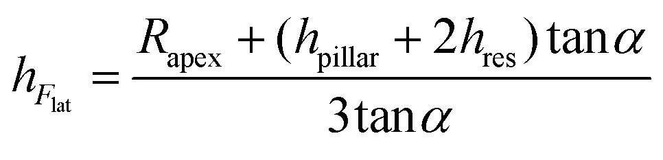
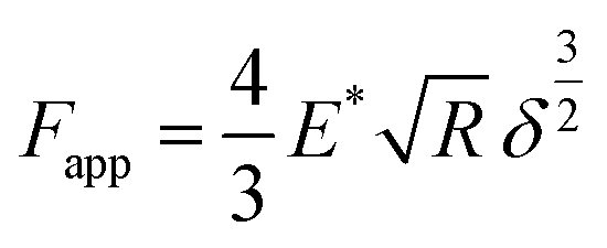
The value of the lateral force applied to the nanopillars corresponding to the applied setpoint force was calculated using eqn (8) (details in the Experimental section). This lateral force is not applied to the apex of the nanopillars but at a certain lower height, due to the possible previous failure of the tip of the pillars and the eventual resting of the AFM tip against the sidewall of the pillars.45 The height of the application of the force (hF_lat) was determined as the height at which the lateral force has to be applied on a conical pillar (with the geometry characteristics of the studied pillars) to yield the maximum stress at a height corresponding to the height of the pillar residues.45 Indeed, as previously pointed out,45 the maximum bending stress in the most loaded section can be written as:
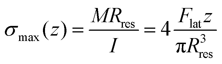 | (1) |
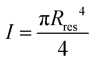 is the area moment of inertia for a circular section. Rres is the radius of the section of the cone corresponding to the height of the residue, which is given as:
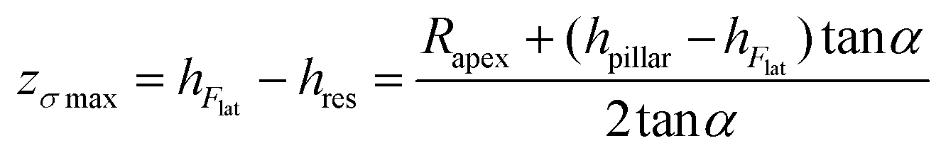
Rres = Rapex + (hpillar − hFlat + z)tan![[thin space (1/6-em)]](https://www.rsc.org/images/entities/char_2009.gif) α α | (2) |
By calculating the derivative of the σmax(z) and solving the following equation:
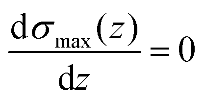 | (3) |
 | (4) |
Therefore, the height of the application of the force can be determined as:
 | (5) |
We found, for eight studied nanopillars, an average value of the lateral force of 654.4 ± 69.3 nN and an average height of the residues of 26.2 ± 2.5 nm, which resulted in an average height of the application of the force of 92.8 ± 1.7 nN (from the base of the pillar). The fracture stress was then calculated by using eqn (1), which resulted in an average value of 3.0 ± 0.3 GPa.
2.4. FEM simulations
The mean elastic modulus determined using the AFM measurements (i.e., E = 17.7 ± 1.5 GPa) was considered as the elastic modulus of the nanopillars in our FEM simulation (Fig. 5a) and the force vs. displacement curve reported in Fig. 5b was obtained. The interaction force between bacteria and the individual nanopillars was calculated from this force vs. displacement curve (purple triangles in Fig. 5b), as the value of the force corresponding to the displacement measured by SEM imaging for the pillars interacting with the bacteria. The mean and standard deviation of the interaction force between the bacteria and individual nanopillars was found to be 88.7 ± 36.1 nN for E = 17.7 GPa (Table 1).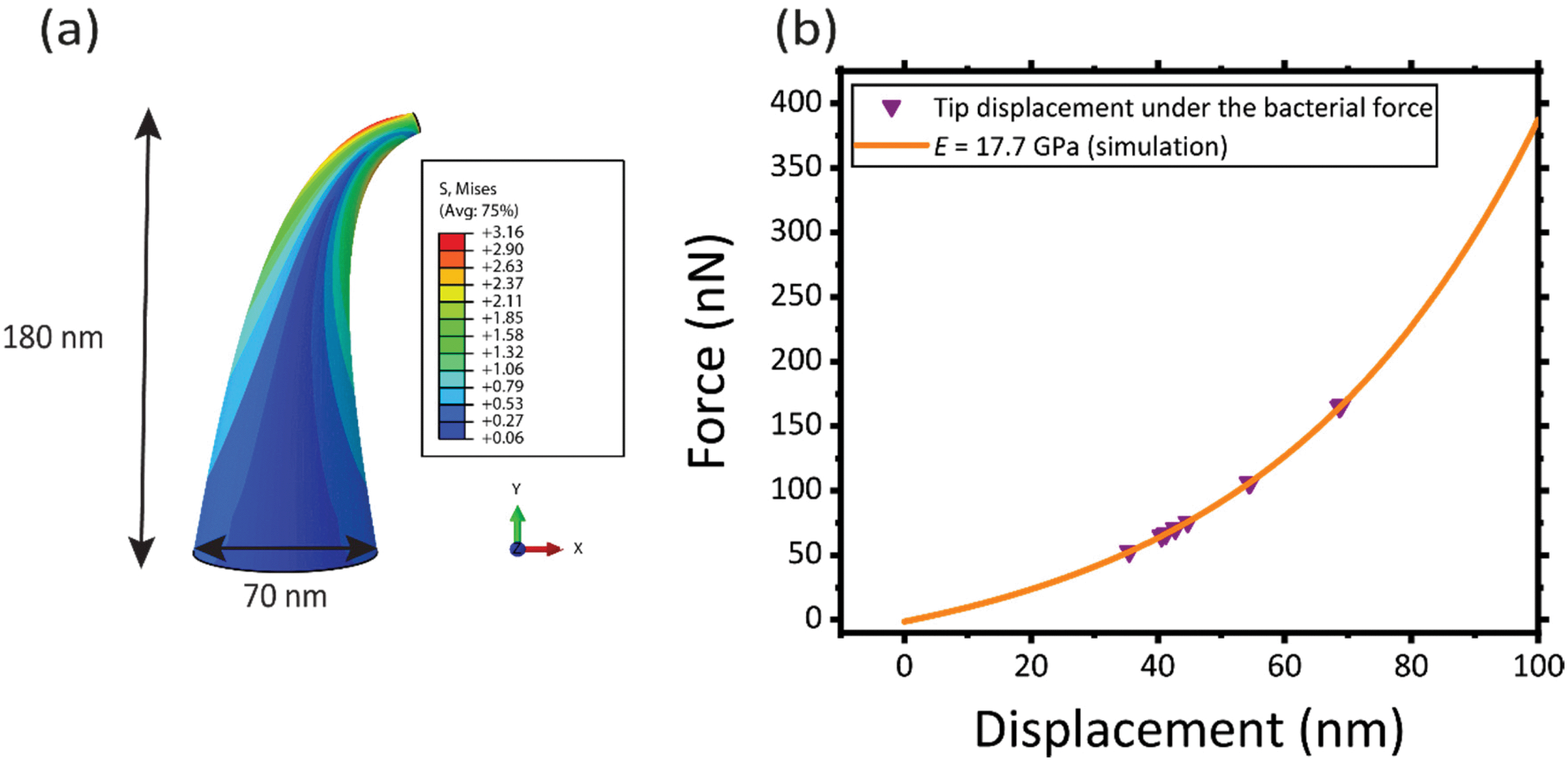 | ||
| Fig. 5 (a) A nanopillar was modeled in Abaqus to simulate the stresses experienced by the nanopillars due to the bacterial force. (b) The orange graph represents the force-displacement curve obtained through FEM (for the nanopillar with E = 17.7 GPa). The displacement of the tip of the nanopillars under bacterial force was fitted in the graph (purple triangles). | ||
| Tip displacement (nm) | Calculated interaction force (nN) (E = 17.7 GPa) |
|---|---|
| 42.8 | 70.4 |
| 54.6 | 106.6 |
| 54.4 | 106.1 |
| 68.7 | 164.8 |
| 41.1 | 66.2 |
| 44.7 | 75.7 |
| 40.6 | 64.9 |
| 36.5 | 55.1 |
In Fig. 5a, the von Mises stress distribution of a pillar undergoing a displacement of 50.3 nm (i.e., the average displacement value due to the interaction with bacteria) is shown. As expected, the maximum stress is located at the border, in a section close to the apex of the pillar, where the force is applied. This indicates that possible fractures of the conical pillars, subjected to the interaction force with the bacteria could occur at the tip of the pillars.
The von Mises stress and the maximum principal stress were equal to 3.16 ± 0.27 GPa and 3.19 ± 0.42 GPa, respectively, which is almost equivalent to the maximum (failure) stress found by AFM measurements (3.0 ± 0.3 GPa). This indicates that, although no visible fracture was observed by SEM imaging, the nanopillars, under the action of the bacteria, are highly deformed and are very close to their failure point.
3. Discussion
The main goal of this study was to quantify the relevant mechanical properties of EBID nanopillars (elastic modulus, fracture force, maximum displacement, and failure stress) and the interaction forces between the nanostructures and the bacterial cells by the combined use of AFM and FEM simulations. The findings of this study could help us optimize the geometry and the mechanical properties of the nanopillars to improve their killing efficiency. Indeed, the results of our previous bacterial culture experiments clearly showed that metal-based EBID-deposited nanostructures have the potential to decorate the surface of biomaterials to damage/kill bacterial cells.32,33 However, while a killing efficiency of the nanopatterns of about 97% was observed against E. coli cells, the killing efficiency was significantly less for S. aurues. In this work, we performed an SEM analysis of the pillars underneath the S. aureus cells that revealed a very high deformation of the tip of the pillars due to the interaction with the bacterial cells. The average lateral displacement was 50.3 ± 9.0 nm.As the killing efficiency is mainly attributed to the capability of the nanopillars to penetrate and damage the cell wall,33,36,37 the non-optimal mechanical properties of the pillars, which result in their excessive deformation could be a possible reason for the low killing efficiency of the pattern against S. aureus. A more in-depth investigation of the mechanical properties of our EBID nanopillars is necessary, to elucidate the possible ways through which our surfaces could be optimized and their killing efficiency can be improved.
We studied, for the first time, the effects of the size on the elastic modulus of EBID structures fabricated using the same deposition parameters (precursor, acceleration voltage, and beam current) and determined the elastic modulus of the nanopillars. The applicability of AFM mechanical characterization techniques (such as the QI mode) to the measurement of the elastic modulus of EBID nanostructures was demonstrated. AFM mechanical experiments showed that the elastic modulus of the EBID pillars is size-independent, as pillars with different sizes (diameter and height) deposited using the same parameters showed no significant differences in their elastic modulus. We could, therefore, conclude that the elastic modulus of our nanopillars could be estimated by AFM mechanical mapping measurements (e.g., QI mode) on larger structures fabricated with the same deposition parameters. The very slight (non-significant) difference found in the elastic modulus of structures with different heights may have been caused by the different electron doses required to deposit pillars with different heights. Therefore, the value of the elastic modulus found for the structure with the closest height to the height of the nanopillars used in the cell experiments (structure with a height of 192 nm) was used in the FEM simulations to determine the bacteria-pillars interaction force. The average elastic modulus for this pillar was 17.7 ± 1.5 GPa (Fig. 3b).
Moreover, the fracture experiments performed on the nanopillars in the AFM contact mode were reported and were shown to represent an effective technique for the evaluation of the fracture strength of nanoscale objects. In our contact mode AFM experiments, we did not observe any failure at the interface between the nanopillars and the substrate, indicating a strong adhesion force of the nanopillars to the substrate The nanopillars were subjected to a bending load, which was applied laterally by the AFM probe at a certain height. By modulating the setpoint force, we applied lateral forces high enough and at a position low enough to cause the failure of the pillars at a visible and easily measurable height (i.e., 26.2 ± 2.5 nm). From the height of the residue, we could calculate the height of the application of the lateral force and, consequently, estimate the failure stress, which was 3.0 ± 0.3 GPa, in very good agreement with our previous results obtained on similar EBID nanopillars with different dimensions.45
We used AFM results, in combination with computational models, to calculate the interaction force between the bacterial cells and the nanopillars and to evaluate the stress state of the nanopillars under the action of bacteria. The elastic modulus measured in the AFM experiments was considered in our computational models and the force vs. displacement curve of the nanopillars was plotted. The interaction force between the bacterial cell and the bent nanopillars was calculated as the value of the force corresponding to the displacement measured by the SEM imaging of the nanopillars interacting with the bacteria. The schematic drawing in Fig. 6 illustrates the steps followed to measure the abovementioned parameters. The estimated value of the interaction force was 88.7 ± 36.1 nN. The maximum value of the von Mises stress (3.16 ± 0.27 GPa) occurred, as expected, in a location close to the apex of the nanopillars, and was almost equivalent to the fracture stress measured through the AFM contact mode experiments (3.0 ± 0.3 GPa). This result indicates that, although no visible fractures of the nanopillars were observed, the pillars were close to their breaking point. This means that the killing efficiency could be affected not only by the excessive elastic deformation of the tip of the conical pillars but also by some relevant plastic deformation phenomena. Furthermore, since the maximum stress is located in a section very close to the apex of the pillars (as indicated by eqn (5) and by the stress distribution in FEM in Fig. 5a), the fracture events could occur in this region under the action of the bacteria and could be not observed by SEM. Indeed, due to the presence of the bacteria attached to the nanopillars, it was not possible to estimate the height of the nanopillars under the bacteria with nanometric accuracy. The possible fracture of the tip of the pillars, increasing the area of the apex of the pillars could further decrease the killing efficiency of the nanopatterned surfaces.
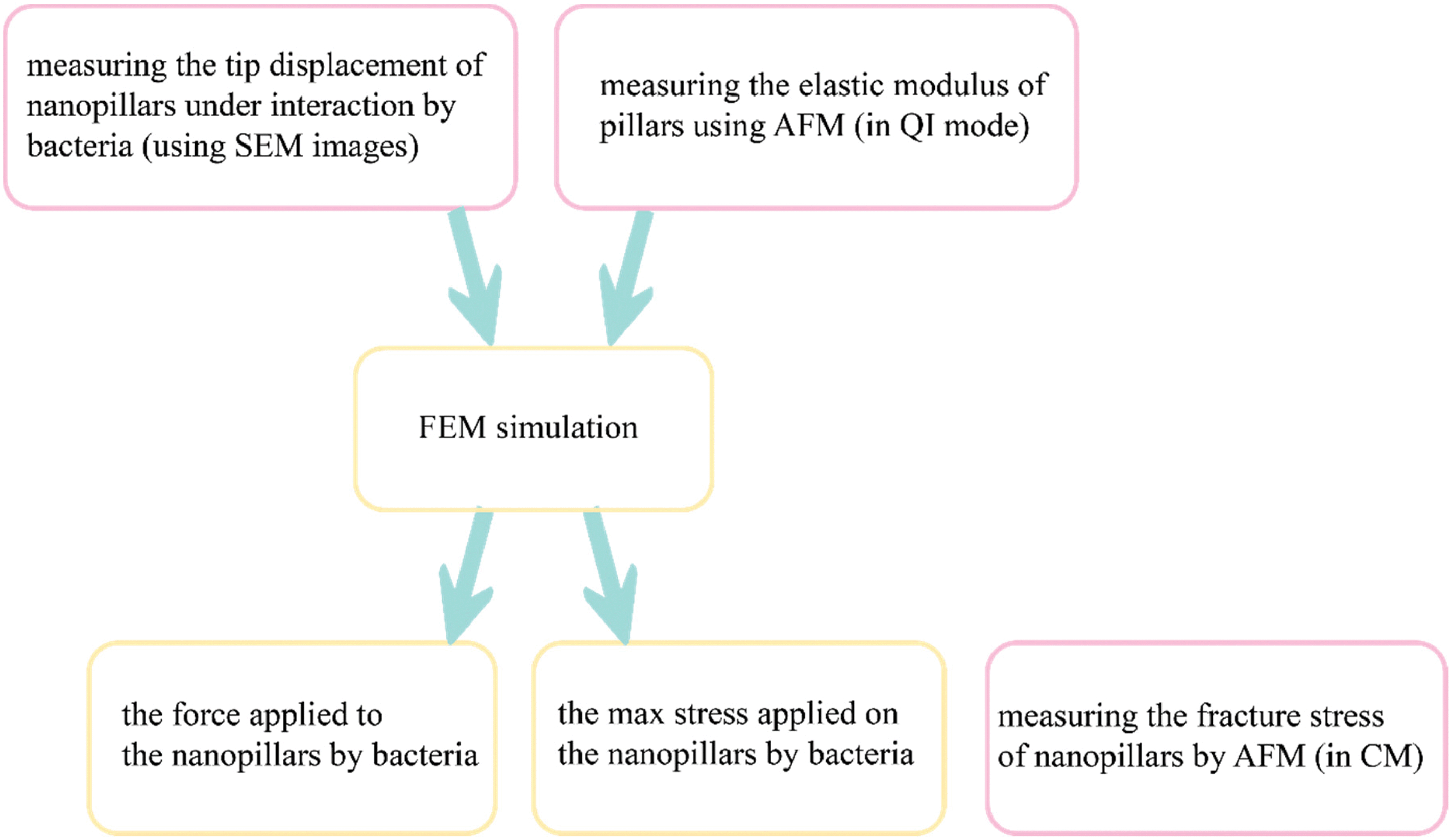 | ||
| Fig. 6 A schematic drawing illustrating the procedure used to evaluate the stress state of our EBID nanopillars and their interaction force with bacteria. Pink blocks indicate the experimentally measured parameters while the yellow blocks indicate the parameters determined by simulation. | ||
From our analysis, we concluded that the killing efficiency of nanopatterned surfaces could be improved by optimizing the mechanical properties of our single pillars. More specifically, by (i) increasing the elastic modulus of the material to reduce the elastic deformation and improve the membrane penetration capability, (ii) increasing the fracture strength (σmax) of the material to reduce eventual plastic deformation and tip fracture phenomena, and (iii) optimizing the geometry of the nanopillars, for example, by increasing the diameter of the cone.
The elastic modulus of the EBID-deposited structures could be increased through several methods including changing the percentage of the main components of the precursor gases: changing the beam current and acceleration voltage,43,46 applying metal purification techniques (e.g., introducing oxygen flux into the chamber during the deposition47,48), substrate annealing,49 electron beam curing,43 electron beam irradiation,50 and laser-assisted purification.51 The abovementioned techniques may lead to higher values of the elastic modulus for the deposited structure. Coating the EBID-deposited structures with other stiff metals using atomic layer deposition (ALD) or evaporation may be another approach to obtain stiffer nanostructures41 with possibly higher values of the killing efficiency.
The maximum stress could be increased by changing the Pt/C ratio in the EBID-deposited structures. The abovementioned purification techniques could help in increasing the Pt content in the final deposited structures, thereby adjusting the maximum (failure) stress. Changing the beam current and voltage is another way to change the composition of the material and modulate the fracture stress.
The geometry of the cone could be easily changed by varying the deposition factors, such as the overall dose, beam energy, current, and defocus.52 Increasing the width of the cones could increase the stiffness and reduce the risk of the fracture of the tip of the cones. This could reduce the bending of the nanopillars and improve their killing efficiency, similar to what was observed by Linklater et al.53 They compared the killing efficiency of carbon nanotubes (CNTs) with the same shape, diameter, and interspace, but with different heights (i.e., 1 μm and 30 μm) against S. aureus. They concluded that shorter CNTs have higher bactericidal efficiencies. This observation could be explained by the fact that for the same applied force, shorter CNTs (higher stiffness) experience lower tip deflections, which result in higher forces being exerted to the bacterial cells. Therefore, changing the geometry of the nanostructures, while remaining in the bactericidal and non-cytotoxic range, can be used to increase the interaction forces and, thus, enhance the bactericidal efficiency of nanopatterned surfaces.
Although the elastic modulus of the EBID-deposited nanostructures considered in the current study is suitable for osteoblast cells, enlarging the patterned area to hundreds of micrometers is a crucial step needed before studies with mammalian cells can be performed. One such method to scale up the deposited area is using a multi-beam scanning electron microscopy. This technique could increase the speed of the process by up to several hundred times (e.g., by focusing 196 beams on the substrate).54
4. Experimental section
4.1. Sample preparation
●For bacterial culture: Double-sided polished 4-inch (diameter: 10.16 cm) Si wafers (thickness 525 ± 25 μm, p-type) were diced into 1 × 1 cm2 specimens (Disco Hi-Tec Europe GMbH, Munich, Germany) and were cleaned with nitric acid.
●For mechanical experiments: An array of 13 × 13 circular holes with a diameter of 10 μm were lithographically defined on the surface of a Si specimen (with the same properties as mentioned in the previous paragraph), so as to obtain a visible structure that could be easily detected by SEM and the optical camera of the AFM microscope. Towards that end, the Si substrate was spin-coated with a photoresist (AZ5214, MicroChem Corp, Westborough, USA) at 4000 rpm, followed by a baking step for 1 min at 110 °C. Then, the pattern was exposed through optical lithography (EVG620 mask aligner, NY, USA) and developed using MF321 (Rohm Haas Electronic Materials, UK). The previous steps were followed by inductive coupled plasma reactive ion etching (ICP RIE) (Adixen, AMS100 Bosch, L-speeder; parameters: SF6 = 200 sccm, O2 = 175 sccm, ICP power = 2000 W, LP power 50 W, temperature = 0 °C) for 10 s to create the intended nanofeatures of black Si, outside of the circular areas (Fig. 7a). The black Si nanofeatures were also used to set the focus and stigmation during the EBID process. The EBID nanostructures were then deposited inside the circles.
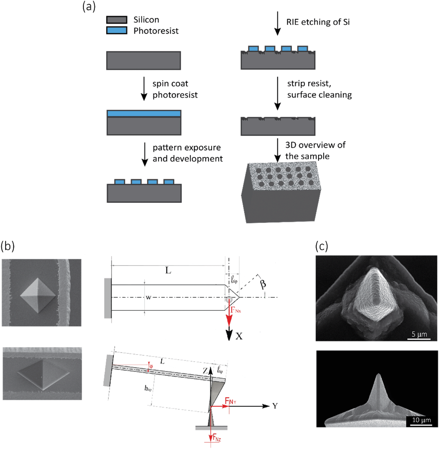 | ||
| Fig. 7 (a) A schematic representation of the process to create black Si on the surface of Si substrate, (b) Left: SEM images showing the top (top) and cross-sectional front (bottom) views of the AFM tip used for the measurement of the fracture force and the maximum displacement of nanopillars. Right: A schematic drawing of the top (top) and cross-sectional side (bottom) views of the AFM probe during the contact with the nanopillars. (c) SEM images showing the top (top) and cross-sectional front (bottom) views of the AFM tip used to measure the elastic modulus. | ||
4.2. (Nano)pillar fabrication using EBID
A dual-beam system (Nova Nano Lab 650 Dual Beam, FEI, Oregon, USA) combining SEM with EBID was used to fabricate the (nano)pillars. Trimethyl(methylcyclopentadienyl)-platinum(IV) or MeCpPt(IV)Me3 was used as the precursor gas. The equipment was operated using an acceleration voltage of 17.8 kV and a beam current of 0.60 nA at a working distance of 5 mm.●For bacterial culture: Under the abovementioned conditions, three areas of 20 × 20 μm2 were covered by the nanopillars. The writing strategy was single dot exposure (i.e., writing the nanopillars one by one), using the stream files generated by a MATLAB (MathWorks, US) code. A stream file was designed to create the nanopillars with a square arrangement with the approximate dimensions of 180 nm (height), 70 nm (base diameter), and 170 nm (center-to-center spacing).
●For fracture force measurements: 11 rows of nanopillars with 20 nanopillars in each row were deposited by using the same conditions as the nanopillars deposited for the bacterial culture. The expected height and diameter were 180 nm and 70 nm, respectively. The interspacing was increased to 340 nm to prevent the neighboring nanopillars from affecting each other during the measurements.
●For elastic modulus measurements: Using the graphical user interface (GUI) accompanying the dual-beam system, a point pitch of 5.43 nm, a pixel dwell time of 10 μs, and different number of passes, we fabricated five pillars with different diameters (i.e., 300, 500, 700, 1000, and 1300 nm), while Z (the parameter of height in the GUI) was set to 20 μm, as well as four pillars with different heights (corresponding to Z = 5, 10, 15, and 20 μm) with a diameter of 1000 nm. The electron dosages applied to create the pillars with different heights were 100, 200, 300, 400, and 500 nC μm−2, respectively. In the case of the pillars with different diameters, the electron dosage was kept constant at 400 nC μm−2.
4.3. Bacterial growth conditions
A Gram-positive bacterial strain (i.e., S. aureus strain RN0450, BEI Resources, Virginia, USA) was used to investigate the bactericidal activity of the nanopatterned surfaces. S. aureus was grown on brain heart infusion (BHI) (Sigma-Aldrich, Missouri, USA) agar plate at 37 °C. The pre-cultures of the bacteria were prepared by inoculating 10 ml autoclaved BHI broth (Sigma-Aldrich, Missouri, USA) with a single colony and cultivation at 140 rpm (kept at 37 °C). The bacterial cells were collected at their logarithmic stage of growth and their optical density at a wavelength of 600 nm (OD600) in the medium solution was adjusted to 0.1.The nanopatterned specimens were immersed in 70% ethanol and exposed to UV light for 20 min prior to the addition of the bacterial culture. A sample containing three nanopatterned areas was inoculated with 1 ml of bacterial suspension in a 24-well plate (Cell Star, Germany). The sample was then incubated at 37 °C for 18 h. Subsequently, the adhered bacteria were fixated for SEM imaging using a fixation solution containing 4% formaldehyde (Sigma-Aldrich, Missouri, USA) and 1% glutaraldehyde (Sigma-Aldrich, Missouri, USA) in 10 mM phosphate buffer. The samples were then washed with MilliQ water and 50%, 70%, and 96% ethanol, respectively, and eventually, soaked in hexamethyldisilazane (HMDS) (Sigma-Aldrich, Missouri, USA) for 30 min and air-dried.
4.4. Morphological characterization of the nanopillars
The resulting nanopatterns were characterized by SEM at different magnifications using a Nova Nano Lab 650 Dual Beam system (FEI, Oregon, USA). The heights and base diameters were measured using 52°-tilt SEM images. The center-to-center spacing of the nanopillars was measured using top-view images.4.5. Quantification of the elastic modulus using AFM
The elastic modulus of the pillars was determined through the AFM experiments performed in the quantitative imaging (QI) mode and using an NM-TC probe (Bruker, Billerica, USA) with a cantilever length of 125 μm, a cantilever width of 30 μm, a spring constant of 350 N m−1, a resonant frequency of 750 kHz, a tip half angle of 45°, and a tip radius of 25 nm (all nominal values) (Fig. 7c). The QI images of the pillars (128 × 128 pixels) were acquired. In the QI mode, a force–distance curve was measured and recorded for each point of the scanned area. The Hertz's contact theory55 was used to calculate, from those curves, the elastic modulus corresponding to each scanned point and to obtain a quantitative map of the elastic modulus.The deflection sensitivity of the cantilever was calibrated with the contact method, i.e., by acquiring a deflection vs. displacement curve on a sapphire surface, resulting in a value of 21.33 nm V−1. Since the accurate estimation of the spring constant of stiff probes cannot be obtained using the direct calibration technique,56 we assumed the spring constant of the probe to equal the nominal value and applied the relative method of calibration to estimate the corresponding tip radius.57,58 A fused-silica reference specimen with a nominal elastic modulus of 72 GPa (test samples kit, Bruker, Billerica, USA), which is relatively close to the elastic modulus of the material of interest, was chosen as the reference material. The tip radius was then adjusted to make the measured elastic modulus of the reference sample equal to the nominal value at an indentation depth of 5 nm. The Poisson's ratio was set to 0.15 (as its nominal value). Under the mentioned condition, a tip radius of 90 nm was found to result in an elastic modulus of 71.13 GPa for the fused silica specimen. The experiment was then conducted on the Si substrate containing the EBID deposited pillars. A constant maximum force of 10 μN was applied to each sample to achieve an indentation of at least 5 nm. A data processing program (JPK SPM, JPK instruments, v6.1, Berlin, Germany) was then used to calculate the elastic modulus of the EBID-deposited material at each point of the scanned area and the same indentation depth of 5 nm as:59,60
 | (6) |
 | (7) |
To prevent the substrate from affecting the final results, the indentation depth should be less than 10% of the pillar height.64,65 In all of our experiments, the indentation depth was 5 nm, which is <7% of the minimum height of the pillars.
The average and standard deviation of the results for each pillar were calculated by extracting and fitting a Gaussian curve to the histogram of the elastic modulus values in the selected areas corresponding to the top of the pillars. The homogeneity of the elastic properties of the pillars with different diameters and heights were evaluated by comparing the mean elastic modulus calculated for areas with different sizes (with increasing distances from the center).
4.6. Quantification of fracture stress using contact mode AFM
The fracture force of the nanopillars was measured using an AFM (JPK Nanowizard 4, Berlin, Germany) operated in the contact mode and using an SSRM-DIA probe (Bruker, USA) (Fig. 7b left) with a cantilever length of 225 μm, a cantilever width of 50 μm, a cantilever thickness of 5 μm, and a spring constant of 27 N m−1, as the nominal values. The line scan rate used was 2 Hz. The tilt angle of the cantilever holder (φ in Fig. 7b, bottom right) was 10°. The calibration of the probe was performed by using the thermal noise method,66 resulting in a spring constant (kc,z) of 26.01 N m−1 and a sensitivity (Sz) of 58.3 nm V−1.The experiments were performed on 10 different nanopillars. The analyzed nanopillars were scanned several times in contact mode, with increasing values of the applied force, obtained by increasing the setpoint force (from 10 nN to 50 nN), until the visible rupture of the nanopillar was observed. After each contact mode scan, the topography of the same area was acquired in the QI mode, with a low setpoint force (10 nN), so as to evaluate any possible changes in the morphology of the nanopillars due to the previously applied force.
The lateral force applied to the nanopillars was calculated as reported elsewhere.45 The applied methodology is briefly described below.
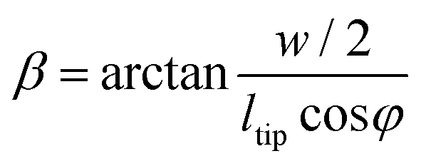
When interacting with the nanopillar, the AFM cantilever can be described as a beam subjected to the combined action of a point load and a bending moment at its free end. Using the beam theory and applying the relevant geometry considerations, FN can be calculated:45
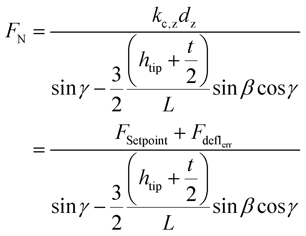 | (8) |
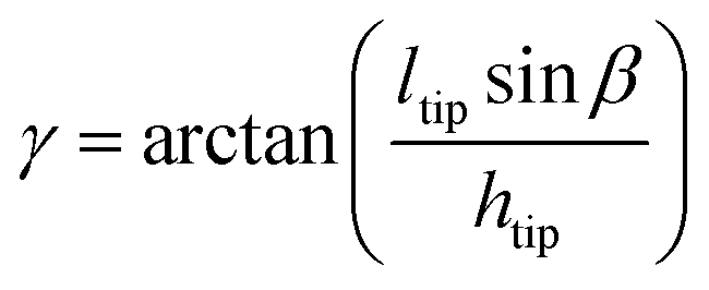
γ, which is the inclination angle of the sidewall of the pyramidal tip, was calculated as:
 | (9) |
The magnitude of the lateral component of the force applied to the pillar can, therefore, be calculated as:
| Flat = FN cos(γ) | (10) |
4.7. FEM model
A nonlinear finite element solver (Abaqus, 6.14) was used to numerically simulate a 3D nanopillar with the same dimensions as those used in our bacterial cell culture experiments (i.e., a base diameter of 70 nm, a height of 180 nm, and a tip diameter of 8 nm) (Fig. 5a). A linear elastic material model and quadratic solid elements (C3D20) were used for all of the simulations. The elastic modulus of the material varied between 1 and 40 GPa. The Poisson's ratio was assumed to equal 0.3. To apply the displacement-controlled boundary conditions, a reference point was defined at the tip of the nanopillar, which was kinematically coupled with the corresponding nodes of the top surface of the nanopillar. The top surface of the nanopillar was free to rotate or move in all other directions. The bottom surface of the nanopillar was clamped. The reaction force was calculated at the reference point. A mesh convergence study was performed by changing the minimum size of the elements from 30 nm to 2 nm. The calculated values of the maximum force varied <5% for the finest mesh. We, therefore, selected the finest element size (i.e., 2 nm) for all of our subsequent simulations.The deflections of the nanopillars when in contact with bacteria were measured using SEM images and were used to back-calculate the interaction forces between the nanopillars and the bacteria. In addition, the numerical simulations were used to calculate the failure lateral force of the nanopillars as the force needed to be applied to the apex of the pillar to obtain the value of the failure stress measured by the contact mode AFM method.
5. Conclusions
In summary, a quantitative study on the mechanical behavior of EBID nanopillars interacting with bacterial cells was performed. To achieve our objective, the challenging issue of the mechanical characterization of single pillars at the nanoscale had to be addressed. A new AFM-based approach was used to measure the elastic modulus and the fracture stress of EBID nanopillars. The elastic modulus of the nanopillars was determined by applying AFM force spectroscopy mechanical mapping (QI mode) to larger structures deposited under similar EBID conditions. Limited influence of the size was observed on the elastic modulus measured on the different studied structures and an elastic modulus of 17.7 ± 1.5 GPa was found for the nanopillars. AFM experiments performed in the contact mode were conducted to push the EBID nanopillars beyond their fracture point. By measuring the applied lateral fracture force and the height of the residue after failure, we were able to determine the fracture stress of the analyzed nanopillars, namely 3.0 ± 0.3 GPa.An FEM model was developed to calculate the interaction force between the nanopillars and the cultured S. aureus bacteria and to determine the stress state of the nanopillars. The interaction force between the nanopillars and bacteria was calculated as 88.7 ± 36.1 nN while the maximum von Mises stress of the nanopillars was 3.16 GPa.
In addition to generating unique quantitative data on the mechanical properties of single EBID nanopillars interacting with S. aureus, the current study resulted in new potential strategies for enhancing the bactericidal efficiency of nanopatterned surfaces, which have to do with the geometry and mechanical properties of the nanopillars.
Author contributions
M.G., L.A., L.E.F.-A., and A.A.Z. conceptualized the study; M.G., L.A., M.J.M., and K.M. designed and performed the experiments and simulations under the supervision of C.W.H., M.K.G., P.-L.H., L.E.F.-A., and A.A.Z.; M.G. wrote the first draft; all authors revised the manuscript; M.K.G., L.E.F.-A., and A.A.Z. acquired the funds.Conflicts of interest
There are no conflicts to declare.Acknowledgements
This research has received funding from the European Research Council under the ERC grant agreement no. [677575]. This research was also partially funded from the TU Delft Cohesion Grant: ‘Diagnosis’ of soft matter on nanopatterned surfaces for better implants. This research was also partially funded from European Union’s Horizon 2020 research and innovation programme under the Marie Skłodowska Curie grant agreement no. [707404].References
- K.-S. Lee, R. H. Kim, D.-Y. Yang and S. H. Park, Prog. Polym. Sci., 2008, 33, 631–681 CrossRef CAS
.
- V. N. Truskett and M. P. Watts, Trends Biotechnol., 2006, 24, 312–317 CrossRef CAS
- K. S. Han, S. H. Hong, K. I. Kim, J. Y. Cho, K. W. Choi and H. Lee, Nanotechnology, 2013, 24, 045304 CrossRef
-
D. J. Resnick, C. Bencher, M. J. Chopra and R. T. Bonnecaze, presented in part at the Alternative Lithographic Technologies VII, 2015 Search PubMed
- C. Steinberg, M. Rumler, M. Runkel, M. Papenheim, S. Wang, A. Mayer, M. Becker, M. Rommel and H.-C. Scheer, Microelectron. Eng., 2017, 176, 22–27 CrossRef CAS
- J. H. Jang, C. K. Ullal, M. Maldovan, T. Gorishnyy, S. Kooi, C. Koh and E. L. Thomas, Adv. Funct. Mater., 2007, 17, 3027–3041 CrossRef CAS
- B. Farshchian, S. M. Hurst, J. Lee and S. Park, J. Micromech. Microeng., 2011, 21(3), 035016 CrossRef
- A. Schleunitz and H. Schift, J. Micromech. Microeng., 2010, 20(9), 095002 CrossRef
- P. Schnauber, R. Schmidt, A. Kaganskiy, T. Heuser, M. Gschrey, S. Rodt and S. Reitzenstein, Nanotechnology, 2016, 27, 195301 CrossRef
- G. Seniutinas, A. Balčytis, I. Reklaitis, F. Chen, J. Davis, C. David and S. Juodkazis, Nanophotonics, 2017, 6, 923–941 Search PubMed
- S. Jesse, A. Y. Borisevich, J. D. Fowlkes, A. R. Lupini, P. D. Rack, R. R. Unocic, B. G. Sumpter, S. V. Kalinin, A. Belianinov and O. S. Ovchinnikova, ACS Nano, 2016, 10, 5600–5618 CrossRef CAS
- R. Winkler, F. P. Schmidt, U. Haselmann, J. D. Fowlkes, B. B. Lewis, G. Kothleitner, P. D. Rack and H. Plank, ACS Appl. Mater. Interfaces, 2017, 9, 8233–8240 CrossRef CAS
- S. Janbaz, N. Noordzij, D. S. Widyaratih, C. W. Hagen, L. E. Fratila-Apachitei and A. A. Zadpoor, Sci. Adv., 2017, 3, eaao1595 CrossRef
- J. Cai, Z. Zhu, P. F. A. Alkemade, E. van Veldhoven, Q. Wang, H. Ge, S. P. Rodrigues, W. Cai and W.-D. Li, Adv. Mater. Interfaces, 2018, 5, 1800203 CrossRef
- S.-H. Ahn, H.-S. Yoon, K.-H. Jang, E.-S. Kim, H.-T. Lee, G.-Y. Lee, C.-S. Kim and S.-W. Cha, CIRP Ann., 2015, 64, 523–526 CrossRef
- B. Salhi, D. Troadec and R. Boukherroub, Nanotechnology, 2017, 28, 205301 CrossRef
- H. Plank, R. Winkler, C. H. Schwalb, J. Hutner, J. D. Fowlkes, P. D. Rack, I. Utke and M. Huth, Micromachines, 2019, 11(1), 48 CrossRef
- W. F. Van Dorp, B. Van Someren, C. W. Hagen, P. Kruit and P. A. Crozier, Nano Lett., 2005, 5, 1303–1307 CrossRef CAS
- N. Silvis-Cividjian and C. W. Hagen, Adv. Imaging Electron Phys., 2006, 143, 1–235 CAS
- S. Randolph, J. Fowlkes and P. Rack, Crit. Rev. Solid State Mater. Sci., 2006, 31, 55–89 CrossRef CAS
- I. Utke, P. Hoffmann and J. Melngailis, J. Vac. Sci. Technol., B: Microelectron. Nanometer Struct.–Process., Meas., Phenom., 2008, 26, 1197–1276 CrossRef CAS
- W. Van Dorp and C. W. Hagen, J. Appl. Phys., 2008, 104, 10 CrossRef
- R. Winkler, J. D. Fowlkes, P. D. Rack and H. Plank, J. Appl. Phys., 2019, 125, 210901 CrossRef
- M. Gabureac, L. Bernau, I. Utke and G. Boero, Nanotechnology, 2010, 21, 115503 CrossRef
- C. H. Schwalb, C. Grimm, M. Baranowski, R. Sachser, F. Porrati, H. Reith, P. Das, J. Muller, F. Volklein, A. Kaya and M. Huth, Sensors, 2010, 10, 9847–9856 CrossRef CAS
-
W. Klauser, M. Bartenwerfer, P. Elfert, E. Krauskopf and S. Fatikow, Micro-Nano-Integration; 6. GMM-WOrkshop, IEEE Xplore, Duisburg, 2016, pp. 1–4 Search PubMed
- C. Haverkamp, K. Hoflich, S. Jackle, A. Manzoni and S. Christiansen, Nanotechnology, 2017, 28, 055303 CrossRef
- S. Sengupta, C. Li, C. Baumier, A. Kasumov, S. Guéron, H. Bouchiat and F. Fortuna, Appl. Phys. Lett., 2015, 106(4), 042601 CrossRef
- J. H. Noh, M. G. Stanford, B. B. Lewis, J. D. Fowlkes, H. Plank and P. D. Rack, Appl. Phys. A, 2014, 117, 1705–1713 CrossRef CAS
- Y. Yang, K. Wang, X. Gu and K. W. Leong, Engineering, 2017, 3, 36–54 CrossRef CAS
- K. Modaresifar, S. Azizian, M. Ganjian, L. E. Fratila-Apachitei and A. A. Zadpoor, Acta Biomater., 2018, 83, 29–36 CrossRef
- D. S. Widyaratih, P. L. Hagedoorn, L. G. Otten, M. Ganjian, N. Tumer, I. Apachitei, C. W. Hagen, L. E. Fratila-Apachitei and A. A. Zadpoor, Nanotechnology, 2019, 30, 20LT01 CrossRef CAS
- M. Ganjian, K. Modaresifar, M. R. Ligeon, L. B. Kunkels, N. Tümer, L. Angeloni, C. W. Hagen, L. G. Otten, P. L. Hagedoorn and I. Apachitei, Adv. Mater. Interfaces, 2019, 1900640 CrossRef
- F. Han, C. Zhu, Q. Guo, H. Yang and B. Li, J. Mater. Chem. B, 2016, 4, 9–26 RSC
- Y. Sun, C. S. Chen and J. Fu, Annu. Rev. Biophys., 2012, 41, 519–542 CrossRef
- P. M. Tsimbouri, L. Fisher, N. Holloway, T. Sjostrom, A. H. Nobbs, R. M. Meek, B. Su and M. J. Dalby, Sci. Rep., 2016, 6, 36857 CrossRef CAS
- S. Ghosh, S. Niu, M. Yankova, M. Mecklenburg, S. M. King, J. Ravichandran, R. K. Kalia, A. Nakano, P. Vashishta and P. Setlow, Sci. Rep., 2017, 7, 17768 CrossRef
- F. Song, M. E. Brasch, H. Wang, J. H. Henderson, K. Sauer and D. Ren, ACS Appl. Mater. Interfaces, 2017, 9, 22176–22184 CrossRef CAS
- V. Friedli, I. Utke, K. Molhave and J. Michler, Nanotechnology, 2009, 20, 385304 CrossRef CAS
- S. Okada, T. Mukawa, R. Kobayashi, M. Ishida, Y. Ochiai, T. Kaito, S. Matsui and J.-I. Fujita, Jpn. J. Appl. Phys., 2006, 45, 5556–5559 CrossRef CAS
- B. B. Lewis, B. A. Mound, B. Srijanto, J. D. Fowlkes, G. M. Pharr and P. D. Rack, Nanoscale, 2017, 9, 16349–16356 RSC
- I. Utke, J. Michler, R. Winkler and H. J. M. Plank, Micromachines, 2020, 11(4), 397 CrossRef
- G. Arnold, R. Winkler, M. Stermitz, A. Orthacker, J. H. Noh, J. D. Fowlkes, G. Kothleitner, M. Huth, P. D. Rack and H. Plank, Adv. Funct. Mater., 2018, 28, 1707387 CrossRef
- A. Reiser, L. Koch, K. A. Dunn, T. Matsuura, F. Iwata, O. Fogel, Z. Kotler, N. J. Zhou, K. Charipar, A. Pique, P. Rohner, D. Poulikakos, S. Lee, S. K. Seol, I. Utke, C. van Nisselroy, T. Zambelli, J. M. Wheeler and R. Spolenak, Adv. Funct. Mater., 2020, 30(28), 1910491 CrossRef CAS
- L. Angeloni, M. Ganjian, M. Nouri-Goushki, M. J. Mirzaali, C. W. Hagen, A. A. Zadpoor, L. E. Fratila-Apachitei and M. K. Ghatkesar, Nanoscale, 2020 Search PubMed
- A. Botman, M. Hesselberth and J. Mulders, Microelectron. Eng., 2008, 85, 1139–1142 CrossRef CAS
- M. Perez-Roldan, J. Mulders and P. Trompenaars, J. Phys. D: Appl. Phys., 2017, 50, 205307 CrossRef
- H. Plank, J. H. Noh, J. D. Fowlkes, K. Lester, B. B. Lewis and P. D. Rack, ACS Appl. Mater. Interfaces, 2014, 6, 1018–1024 CrossRef CAS
- M. H. Ervin, D. Chang, B. Nichols, A. Wickenden, J. Barry and J. Melngailis, J. Vac. Sci. Technol., B: Microelectron. Nanometer Struct.–Process., Meas., Phenom., 2007, 25, 2250–2254 CrossRef CAS
- S. Mehendale, J. Mulders and P. Trompenaars, Microelectron. Eng., 2015, 141, 207–210 CrossRef CAS
- M. G. Stanford, B. B. Lewis, J. H. Noh, J. D. Fowlkes and P. D. Rack, ACS Appl. Mater. Interfaces, 2015, 7, 19579–19588 CrossRef CAS
- B. B. Lewis, B. A. Mound, B. Srijanto, J. D. Fowlkes, G. M. Pharr and P. D. Rack, Nanoscale, 2017, 9, 16349–16356 RSC
- D. P. Linklater, M. De Volder, V. A. Baulin, M. Werner, S. Jessl, M. Golozar, L. Maggini, S. Rubanov, E. Hanssen, S. Juodkazis and E. P. Ivanova, ACS Nano, 2018, 12, 6657–6667 CrossRef CAS
- P. Post, A. Mohammadi-Gheidari, C. W. Hagen and P. Kruit, J.
Vac. Sci. Technol., B, 2011, 29(6), 06F310 CrossRef
- A. Sobiepanek, M. Milner-Krawczyk, M. Lekka and T. Kobiela, Biosens. Bioelectron., 2017, 93, 274–281 CrossRef CAS
- Y. Tian, C. Zhou, F. Wang, J. Zhang, Z. Guo and D. Zhang, Rev. Sci. Instrum., 2018, 89, 125119 CrossRef
- P. Xavier and S. Bose, Macromolecules, 2016, 49, 1036–1048 CrossRef CAS
- A. Pakzad, J. Simonsen and R. S. Yassar, Compos. Sci. Technol., 2012, 72, 314–319 CrossRef CAS
- M. Ren, T. Shi, D. J. Corr and S. P. Shah, J. Wuhan Univ. Technol., Mater. Sci. Ed., 2019, 34, 893–899 CrossRef CAS
- C. Li, M. Ostadhassan, T. Gentzis, L. Kong, H. Carvajal-Ortiz and B. Bubach, Mar. Pet. Geol., 2018, 96, 128–138 CrossRef CAS
- H. Gercek, Int. J. Rock Mech. Min. Sci., 2007, 44, 1–13 CrossRef
- J. Merker, D. Lupton, M. Töpfer and H. Knake, Platinum Met. Rev., 2001, 45, 74–82 CAS
- R. Jana, D. Savio, V. L. Deringer and L. Pastewka, Modell. Simul. Mater. Sci. Eng., 2019, 27, 085009 CrossRef CAS
- Y. N. Xu, M. N. Liu, M. C. Wang, A. Oloyede, J. M. Bell and C. Yan, J. Appl. Phys., 2015, 118, 145301 CrossRef
- J. I. Kilpatrick, I. Revenko and B. J. Rodriguez, Adv. Healthcare Mater., 2015, 4, 2456–2474 CrossRef CAS
- L.-O. Heim, T. S. Rodrigues and E. Bonaccurso, Colloids Surf., A, 2014, 443, 377–383 CrossRef CAS
| This journal is © The Royal Society of Chemistry 2020 |